JP7127042B2 - PHOTOELECTRIC CONVERSION MODULE AND METHOD OF MANUFACTURING PHOTOELECTRIC CONVERSION MODULE - Google Patents
PHOTOELECTRIC CONVERSION MODULE AND METHOD OF MANUFACTURING PHOTOELECTRIC CONVERSION MODULE Download PDFInfo
- Publication number
- JP7127042B2 JP7127042B2 JP2019542010A JP2019542010A JP7127042B2 JP 7127042 B2 JP7127042 B2 JP 7127042B2 JP 2019542010 A JP2019542010 A JP 2019542010A JP 2019542010 A JP2019542010 A JP 2019542010A JP 7127042 B2 JP7127042 B2 JP 7127042B2
- Authority
- JP
- Japan
- Prior art keywords
- photoelectric conversion
- electrode layer
- region
- grid
- conversion module
- Prior art date
- Legal status (The legal status is an assumption and is not a legal conclusion. Google has not performed a legal analysis and makes no representation as to the accuracy of the status listed.)
- Active
Links
Images


Classifications
-
- H—ELECTRICITY
- H10—SEMICONDUCTOR DEVICES; ELECTRIC SOLID-STATE DEVICES NOT OTHERWISE PROVIDED FOR
- H10F—INORGANIC SEMICONDUCTOR DEVICES SENSITIVE TO INFRARED RADIATION, LIGHT, ELECTROMAGNETIC RADIATION OF SHORTER WAVELENGTH OR CORPUSCULAR RADIATION
- H10F19/00—Integrated devices, or assemblies of multiple devices, comprising at least one photovoltaic cell covered by group H10F10/00, e.g. photovoltaic modules
- H10F19/30—Integrated devices, or assemblies of multiple devices, comprising at least one photovoltaic cell covered by group H10F10/00, e.g. photovoltaic modules comprising thin-film photovoltaic cells
- H10F19/31—Integrated devices, or assemblies of multiple devices, comprising at least one photovoltaic cell covered by group H10F10/00, e.g. photovoltaic modules comprising thin-film photovoltaic cells having multiple laterally adjacent thin-film photovoltaic cells deposited on the same substrate
- H10F19/35—Structures for the connecting of adjacent photovoltaic cells, e.g. interconnections or insulating spacers
-
- H—ELECTRICITY
- H10—SEMICONDUCTOR DEVICES; ELECTRIC SOLID-STATE DEVICES NOT OTHERWISE PROVIDED FOR
- H10F—INORGANIC SEMICONDUCTOR DEVICES SENSITIVE TO INFRARED RADIATION, LIGHT, ELECTROMAGNETIC RADIATION OF SHORTER WAVELENGTH OR CORPUSCULAR RADIATION
- H10F71/00—Manufacture or treatment of devices covered by this subclass
- H10F71/138—Manufacture of transparent electrodes, e.g. transparent conductive oxides [TCO] or indium tin oxide [ITO] electrodes
-
- H—ELECTRICITY
- H10—SEMICONDUCTOR DEVICES; ELECTRIC SOLID-STATE DEVICES NOT OTHERWISE PROVIDED FOR
- H10F—INORGANIC SEMICONDUCTOR DEVICES SENSITIVE TO INFRARED RADIATION, LIGHT, ELECTROMAGNETIC RADIATION OF SHORTER WAVELENGTH OR CORPUSCULAR RADIATION
- H10F77/00—Constructional details of devices covered by this subclass
- H10F77/20—Electrodes
- H10F77/206—Electrodes for devices having potential barriers
- H10F77/211—Electrodes for devices having potential barriers for photovoltaic cells
- H10F77/215—Geometries of grid contacts
-
- H—ELECTRICITY
- H10—SEMICONDUCTOR DEVICES; ELECTRIC SOLID-STATE DEVICES NOT OTHERWISE PROVIDED FOR
- H10F—INORGANIC SEMICONDUCTOR DEVICES SENSITIVE TO INFRARED RADIATION, LIGHT, ELECTROMAGNETIC RADIATION OF SHORTER WAVELENGTH OR CORPUSCULAR RADIATION
- H10F77/00—Constructional details of devices covered by this subclass
- H10F77/20—Electrodes
- H10F77/244—Electrodes made of transparent conductive layers, e.g. transparent conductive oxide [TCO] layers
Landscapes
- Photovoltaic Devices (AREA)
Description
本発明は、グリッド電極を有する光電変換モジュールと、光電変換モジュールを製造する方法に関する。 TECHNICAL FIELD The present invention relates to a photoelectric conversion module having grid electrodes and a method of manufacturing the photoelectric conversion module.
複数の光電変換セルを含む太陽電池モジュールのような光電変換モジュールが知られている(下記特許文献1)。特許文献1に記載されたような集積型薄膜光電変換モジュールでは、光電変換セルは、受光面に位置する透明電極層と、受光面とは反対側の面に位置する裏面電極層と、透明電極層と裏面電極層との間の光電変換層と、を有する。
A photoelectric conversion module such as a solar cell module including a plurality of photoelectric conversion cells is known (
透明電極層の電気抵抗値は、一般に、金属からなる不透明の電極層の電気抵抗値よりも高い。したがって、光電変換によって生じた電流が透明電極層を流れる場合に、透明電極層の電気抵抗値に起因する電力のロスが発生する。この透明電極層での電力のロスを低減するため、透明電極層の上に細線状の金属からなるグリッド電極(集電電極)が設けられることがある。 The electrical resistance value of the transparent electrode layer is generally higher than the electrical resistance value of the opaque electrode layer made of metal. Therefore, when a current generated by photoelectric conversion flows through the transparent electrode layer, power loss occurs due to the electrical resistance value of the transparent electrode layer. In order to reduce the power loss in this transparent electrode layer, a grid electrode (collecting electrode) made of a thin metal wire is sometimes provided on the transparent electrode layer.
特許文献1に記載された光電変換モジュールでは、透明電極層に流れる電流がグリッド電極に集電されることで、透明電極層を流れる電流経路が短くなる。そのため、透明電極層の電気抵抗値に起因する電力のロスを低減できる。しかしながら、グリッド電極は、一般に非透明であるため、光電変換層へ入射する光を遮ることになる。したがって、光電変換層に到達する光の減少により、光電変換セルで発生する短絡電流(Isc)が小さくなる。
In the photoelectric conversion module described in
よって、透明電極層の電気抵抗値に起因する電力のロスという課題と、グリッド電極による光の遮蔽に起因する短絡電流の低減という課題の両方のバランスをとることが望まれる。 Therefore, it is desirable to strike a balance between the problem of power loss caused by the electrical resistance of the transparent electrode layer and the problem of reducing the short-circuit current caused by the light shielding by the grid electrode.
一態様に係る光電変換モジュールは、第1電極層と、第2電極層と、前記第1電極層と前記第2電極層との間の光電変換層と、を含む帯状の光電変換セルと、前記光電変換セルにおいて第1方向に並んで設けられ、前記第1方向に交差する方向に延びる複数のグリッド電極と、を有し、前記第1電極層と前記第2電極層の少なくとも一方は透明電極層であり、前記透明電極層は、第1領域及び第2領域を含み、前記第2領域は、前記第1領域におけるシート抵抗よりも小さいシート抵抗、前記第1領域における膜厚よりも大きい膜厚、又は前記第1領域における透過率よりも小さい透過率を有し、前記第1領域において前記第1方向に互いに隣り合う前記グリッド電極どうしの間隔は、前記第2領域において前記第1方向に互いに隣り合う前記グリッド電極どうしの間隔よりも小さい。 A photoelectric conversion module according to one aspect includes a strip-shaped photoelectric conversion cell including a first electrode layer, a second electrode layer, and a photoelectric conversion layer between the first electrode layer and the second electrode layer; a plurality of grid electrodes arranged in a first direction in the photoelectric conversion cell and extending in a direction crossing the first direction, wherein at least one of the first electrode layer and the second electrode layer is transparent An electrode layer, wherein the transparent electrode layer includes a first region and a second region, wherein the second region has a sheet resistance smaller than the sheet resistance in the first region and a film thickness greater than the film thickness in the first region The distance between the grid electrodes that have a transmittance smaller than the film thickness or the transmittance in the first region and are adjacent to each other in the first direction in the first region is equal to the first direction in the second region is smaller than the interval between the grid electrodes adjacent to each other.
一態様に係る光電変換モジュールを製造する方法は、基板上に、第1電極層と、第2電極層と、前記第1電極層と前記第2電極層との間の光電変換層と、を含む帯状の光電変換セルを形成するセル形成工程であって、前記第1電極層と前記第2電極層の少なくとも一方は透明電極層であるセル形成工程と、前記透明電極層のシート抵抗、膜厚又は透過率を測定する工程と、前記光電変換セルにおいて第1方向に並んで設けられ、前記第1方向に交差する方向に延びる複数のグリッド電極を形成するグリッド形成工程と、を有し、前記グリッド形成工程では、大きいシート抵抗を有する領域、小さい膜厚を有する領域、又は大きい透過率を有する領域ほどグリッド電極のどうしの間隔が小さくなるように、グリッド電極が形成される。 A method for manufacturing a photoelectric conversion module according to one aspect includes forming, on a substrate, a first electrode layer, a second electrode layer, and a photoelectric conversion layer between the first electrode layer and the second electrode layer. a cell forming step of forming a strip-shaped photoelectric conversion cell comprising: a cell forming step in which at least one of the first electrode layer and the second electrode layer is a transparent electrode layer; a sheet resistance of the transparent electrode layer, a film a step of measuring thickness or transmittance; and a grid forming step of forming a plurality of grid electrodes arranged side by side in the first direction in the photoelectric conversion cell and extending in a direction intersecting the first direction, In the grid forming step, the grid electrodes are formed so that the intervals between the grid electrodes become smaller in regions having a higher sheet resistance, a region having a smaller film thickness, or a region having a higher transmittance.
以下、図面を参照して、実施形態について説明する。以下の図面において、同一又は類似の部分には、同一又は類似の符号を付している。ただし、図面は模式的なものであり、各寸法の比率等は現実のものとは異なることがあることに留意すべきである。 Embodiments will be described below with reference to the drawings. In the following drawings, the same or similar parts are given the same or similar reference numerals. However, it should be noted that the drawings are schematic, and the ratio of each dimension may differ from the actual one.
(第1実施形態)
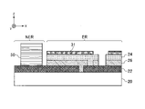
図1は、第1実施形態に係る光電変換モジュールの模式的上面図である。図2は、図1の領域2Rにおける光電変換モジュールの模式的上面図である。図3は、図2の3A-3A線に沿った光電変換モジュールの模式的断面図である。図4は、図2の領域4Rにおける光電変換モジュールの模式的斜視図である。図5は、図1の5A-5A線に沿った光電変換モジュールの模式的断面図である。図6は、図1の領域6Rにおける光電変換モジュールの模式的上面図である。図7は、図1の領域7Rにおける光電変換モジュールの模式的上面図である。(First embodiment)
FIG. 1 is a schematic top view of a photoelectric conversion module according to the first embodiment. FIG. 2 is a schematic top view of the photoelectric conversion module in
本実施形態に係る光電変換モジュール10は、基板20上に集積された複数の光電変換セル12を含む集積型の薄膜光電変換モジュールであってよい。好ましくは、光電変換モジュール10は、光エネルギーを電気的エネルギーに変換する太陽電池モジュールである。基板20は、例えばガラス、セラミックス、樹脂又は金属などによって構成されていてよい。
The
光電変換セル12は、基板20の主面に直交する方向から見て、実質的に帯状の形状を有していてよい。各々の光電変換セル12は第1方向(図のY方向)に長く延びていてよい。また、複数の光電変換セル12は、第1方向に交差する第2方向(図のX方向)に並んでいる。互いに隣接する光電変換セル12は、第1方向に延びる分割部P1,P2,P3によって互いに分断されていてよい。
The
各々の光電変換セル12は、少なくとも、第1電極層22と、第2電極層24と、光電変換層26と、を含んでいてよい。光電変換層26は、第1電極層22と第2電極層24との間に設けられる。第1電極層22は、光電変換層26と基板20との間に設けられている。第2電極層24は、光電変換層26に関して基板20とは反対側に位置する。
Each
本実施形態では、第2電極層24は透明電極層によって構成されていてよい。第2電極層24が透明電極層によって構成されている場合、光電変換層26へ入射、又は光電変換層26から出射する光は、第2電極層24を通過する。
In this embodiment, the
第2電極層24が透明電極層によって構成される場合、第1電極層22は、不透明電極層によって構成されていてもよく、透明電極層によって構成されていてもよい。CIS系の光電変換モジュールの一例では、VI族元素に対する耐腐食性の観点から、第1電極層22は、例えば、モリブデン、チタン又はクロムのような金属によって形成されることが好ましい。
When the
本実施形態では、好ましい一例として、第2電極層24は、n型半導体、より具体的には、n型の導電性を有し、禁制帯幅が広く、比較的低抵抗の材料によって形成される。第2電極層24は、例えば、III族元素を添加した酸化亜鉛(ZnO)や、酸化インジウムスズ(Indium Tin Oxide: ITO)によって構成されていてよい。この場合、第2電極層24は、n型半導体と透明電極層の機能を兼ねることができる。
In this embodiment, as a preferred example, the
光電変換層26は、例えば、p型の半導体を含んでいてよい。CIS系の光電変換モジュールの一例では、光電変換層26は、I族元素(Cu、Ag、Au等)、III族元素(Al、Ga、In等)及びVI族元素(O、S、Se、Te等)を含む化合物半導体で形成される。光電変換層26は、前述したものに限定されず、光電変換を起こす任意の材料によって構成されていてよい。
The
光電変換セル12の構成は、上記態様に限定されず、様々な態様をとり得ることに留意されたい。例えば、光電変換セル12は、n型半導体とp型半導体の両方が第1電極層と第2電極層との間に挟まれた構成を有していてもよい。この場合、第2電極層はn型半導体によって構成されていなくてよい。また、光電変換セル12は、p-n結合型の構造に限らず、n型半導体とp型半導体との間に真性半導体層(i型半導体)を含むp-i-n結合型の構造を有していてもよい。
It should be noted that the configuration of the
光電変換セル12は、光電変換層26と第2電極層24との間に不図示のバッファ層を有していてもよい。この場合、バッファ層は、第2電極層24と同じ導電型を有する半導体材料であってもよく、異なる導電型を有する半導体材料であってもよい。バッファ層は、第2電極層24よりも電気抵抗の高い材料によって構成されていればよい。CIS系の光電変換モジュールの一例では、バッファ層は、Zn系バッファ層、Cd系バッファ層又はIn系バッファ層であってよい。Zn系バッファ層は、例えばZnS、ZnO、Zn(OH)若しくはZnMgOや、これらの混晶又は積層体であってよい。Cd系バッファ層は、例えばCdS、CdO若しくはCd(OH)や、これらの混晶又は積層体であってよい。In系バッファ層は、例えばInS、InO若しくはIn(OH)や、これらの混晶又は積層体であってよい。
The
互いに隣接する光電変換セル12の第1電極層22は、分割部P1によって互いに電気的に分断されている。同様に、互いに隣接する光電変換セル12の第2電極層24は、分割部P3によって互いに電気的に分断されている。互いに隣接する光電変換セル12の光電変換層26は、分割部P2,P3によって互いに分断されている。
The first electrode layers 22 of the
光電変換モジュール10は、互いに隣接する光電変換セル12どうしの間に電気接続部34を有していてよい。電気接続部34は、互いに隣接する光電変換セル12どうしを電気的に直列に接続する。本実施形態では、電気接続部34は、第2電極層24から連続する部分によって形成されている。この場合、電気接続部34は、第2電極層24と同じ材料から構成されていてよい。この代わりに、電気接続部34は、第2電極層24と異なる導電材料から構成されていてもよい。例えば、電気接続部34は、後述する第1グリッド電極31又は第2グリッド電極32を構成する材料と同じ材料から構成されていてもよい。
The
電気接続部34は、第2分割部P2のところで光電変換モジュール10の厚み方向に延びることで、一方の光電変換セル12の第1電極層22と他方の光電変換セル12の第2電極層24とを互いに電気的に接続する。
The
光電変換モジュール10は、各々の光電変換セル12において第1方向(図のY方向)に並んで設けられた複数の第1グリッド電極31を有する。各々の第1グリッド電極31は、第1方向に交差する第2方向(図のX方向)に延びている。第1グリッド電極31は、各々の光電変換セル12の第2電極層24上に設けられていてよい。第1グリッド電極31は、第2電極層24を構成する透明電極層よりも導電性の高い材料によって構成されていてよい。第1グリッド電極31は、この透明電極層に直接接していてよい。第1方向(図のY方向)における第1グリッド電極31の幅は、例えば5~100μmであってよい。第1グリッド電極31の厚みは、例えば0.1~20μmであってよい。
The
必要に応じて、第1方向(図のY方向)に延びる第2グリッド電極32が、第2方向(図のX方向)における第1グリッド電極31の端部に設けられていてもよい。第2グリッド電極32は、第1グリッド電極31の一方の端部にて、第1グリッド電極31と連結されている。第2方向(図のX方向)における第2グリッド電極32の幅は、例えば5~200μmであってよい。第2グリッド電極32の厚みは、例えば0.1~20μmであってよい。
If necessary, a
第1グリッド電極31と第2グリッド電極32(又は電気接続部34)との交点における第1グリッド電極31と第2グリッド電極32(又は電気接続部34)の少なくとも一方、好ましくは両方の厚みは、当該交点から離れた位置における第1グリッド電極31と第2グリッド電極32(又は電気接続部34)の厚みより厚いことが好ましい。例えば、第1グリッド電極31の厚みが、第1グリッド電極31と第2グリッド電極32(又は電気接続部34)との交点に向かうにつれて徐々に厚くなっていてよい。また、第2グリッド電極32(又は電気接続部34)の厚みが、第1グリッド電極31と第2グリッド電極32(又は電気接続部34)との交点に向かうにつれて徐々に厚くなっていてもよい。
The thickness of at least one, preferably both, of the
各々の光電変換セル12の光電変換層26に光が照射されると起電力が生じ、第1電極層22及び第2電極層24がそれぞれ正極及び負極となる。したがって、ある光電変換セル12で生じた自由電子の一部は、第2電極層24から直接電気接続部34を通って、隣接する光電変換セル12の第1電極層22に移動する。また、ある光電変換セル12で生じた自由電子の別の一部は、第2電極層24から第1グリッド電極31及び第2グリッド電極32を介して電気接続部34を通り、隣接する光電変換セル12の第1電極層22に移動する。このように、光電変換セル12で生じた自由電子は、第2方向(図のX方向)に複数の光電変換セル12を通って流れることになる。
When the
光電変換モジュール10は、電力を光電変換モジュール10へ供給又は光電変換モジュール10から取り出すための配線50を有する。配線50は、第2方向(図のX方向)における光電変換モジュール10の端に位置する光電変換セル12に隣接して設けられていてよい。
The
本実施形態において、第2電極層24を構成する透明電極層は、図2に示すような領域2Rと、図6に示すような領域6Rと、を含んでいてよい。領域2Rと領域6Rは、同一の光電変換セル12内に配置されている。領域2Rにおいて第1方向(Y方向)に互いに隣り合う第1グリッド電極31どうしの間隔は、領域6Rにおいて第1方向(Y方向)に互いに隣り合う第1グリッド電極31どうしの間隔よりも小さい。ここで、第2電極層24の領域6Rは、領域2Rにおけるシート抵抗よりも小さいシート抵抗、領域2Rにおける膜厚よりも大きい膜厚、又は領域2Rにおける透過率よりも小さい透過率を有する。なお、上述した第1グリッド電極31の間隔とは、任意の第1グリッド電極31の中心線と隣り合う第1グリッド電極31の中心線との間隔である。
In this embodiment, the transparent electrode layer forming the
また、本実施形態において、第2電極層24は、図7に示すような領域7Rをさらに含んでいてもよい。領域6Rと領域7Rとは、互いに異なる光電変換セル12内に配置されている。
Moreover, in the present embodiment, the
領域7Rにおいて第1方向(Y方向)に互いに隣り合う第1グリッド電極31どうしの間隔は、領域6Rにおいて第1方向(Y方向)に互いに隣り合う第1グリッド電極31どうしの間隔よりも小さい。ここで、第2電極層24の領域6Rは、領域7Rにおけるシート抵抗よりも小さいシート抵抗、領域7Rにおける膜厚よりも大きい膜厚、又は領域7Rにおける透過率よりも小さい透過率を有する。
The interval between the
より好ましくは、光電変換モジュール10の第2電極層24は、シート抵抗、膜厚又は透過率に分布を有し、第1方向(Y方向)に互いに隣り合う第1グリッド電極31のどうしの間隔は、シート抵抗が大きいほど小さく、膜厚が小さいほど小さく、又は透過率が大きいほど小さい。
More preferably, the
透明電極層のシート抵抗が大きい領域ほど、第1グリッド電極31どうしの間隔を狭くすると、透明電極層と第1グリッド電極31の両方を合わせた電気抵抗値の分布が均一に近づく。このように全体のシート抵抗を均一に近づけるとともに、不必要な領域において第1グリッド電極31の密度(光電変換モジュールを平面視した場合の、単位面積あたりグリッド電極の面積密度)を低くすることによって、透明電極層の電気抵抗値に起因する電力のロスという課題と、第1グリッド電極による光の遮蔽に起因する短絡電流の低減という課題の両方のバランスをとることができる。
If the interval between the
また、一般には、透明電極層の膜厚が小さいほど、透明電極層のシート抵抗は高くなると考えられる。さらに、透明電極層の透過率が大きいほど、透明電極層のシート抵抗は高くなると考えられる。これは、透明電極層の透過率が大きい場合、一般には透明電極層の膜厚が小さい、又は透明電極層のキャリア濃度が低いためと考えられる。 In general, it is considered that the smaller the film thickness of the transparent electrode layer, the higher the sheet resistance of the transparent electrode layer. Furthermore, it is considered that the higher the transmittance of the transparent electrode layer, the higher the sheet resistance of the transparent electrode layer. This is probably because when the transmittance of the transparent electrode layer is high, the film thickness of the transparent electrode layer is generally small, or the carrier concentration of the transparent electrode layer is low.
したがって、透明電極層の膜厚が小さいほど、又は透明電極層の透過率が大きいほど第1グリッド電極31どうしの間隔を狭くすることで、透明電極層と第1グリッド電極31の両方を合わせた電気抵抗値の分布が均一に近づくと考えられる。この場合であっても、全体のシート抵抗を均一に近づけるとともに、不必要な領域において第1グリッド電極31の密度を低くすることによって、透明電極層の電気抵抗値に起因する電力のロスという課題と、第1グリッド電極による光の遮蔽に起因する短絡電流の低減という課題の両方のバランスをとることができる。
Therefore, the smaller the film thickness of the transparent electrode layer, or the larger the transmittance of the transparent electrode layer, the narrower the interval between the
ここで、透明電極層の膜厚又は透過率は、製造ライン中において透明電極層のシート抵抗よりも容易に測定することができる。したがって、透明電極層の膜厚又は透過率に応じて第1グリッド電極31の間隔を設定する場合、光電変換モジュール10の製造上のメリットが高い。
Here, the film thickness or transmittance of the transparent electrode layer can be measured more easily than the sheet resistance of the transparent electrode layer in the production line. Therefore, setting the interval between the
図8は、第1変形例に係る第1グリッド電極31と第2グリッド電極32の連結部分の模式的上面図である。第1変形例において、第1方向(Y方向)における第1グリッド電極31の幅は、第2グリッド電極32に近づくにつれて広くなっている。具体的には、第1方向(Y方向)における第1グリッド電極31の幅は、第2グリッド電極32に近づくにつれて徐々に拡大している。
FIG. 8 is a schematic top view of the connecting portion between the
これとは逆に、第2方向(X方向)における第2グリッド電極32の幅が、第1グリッド電極31に近づくにつれて徐々に拡大していてもよい。
Conversely, the width of the
図9は、第2変形例に係る第1グリッド電極31と第2グリッド電極32の連結部分の模式的上面図である。第2変形例において、第1方向(Y方向)における第1グリッド電極31の幅は、第2グリッド電極32に近づくにつれて広くなっている。具体的には、第1方向(Y方向)における第1グリッド電極31の幅は、第2グリッド電極32に近づくにつれて段階的に拡大している。
FIG. 9 is a schematic top view of the connecting portion of the
これとは逆に、第2方向(X方向)における第2グリッド電極32の幅が、第1グリッド電極31に近づくにつれて徐々に段階的に拡大していてもよい。
Conversely, the width of the
第1変形例及び第2変形例では、第1グリッド電極31と第2グリッド電極32の連結部分の領域を大きくすることによって、第1グリッド電極31と第2グリッド電極32との連結部分における電気的な接続不良又は電気抵抗の増大を抑制することができる。
In the first modified example and the second modified example, by enlarging the area of the connecting portion between the
図10は、第3変形例に係る第1グリッド電極31と第2グリッド電極32の連結部分の模式的上面図である。第3変形例において、第1グリッド電極31は、第2グリッド電極32に近づくとともに第1方向(Y方向)に曲がっている。このように第1グリッド電極31と第2グリッド電極32との連結箇所が曲がっていることにより、第1グリッド電極31に流れる電流が連結箇所で反射することを低減できる。
FIG. 10 is a schematic top view of the connecting portion of the
また、他の変形例として、第1グリッド電極31は、第2グリッド電極32に近づくとともに厚みが大きくなってもよい。
As another modification, the thickness of the
次に、図11~図16を参照し、一実施形態に係る光電変換モジュールを製造する方法について説明する。なお、以下の各ステップにおいて、各層は、スパッタ法や蒸着法などの成膜手段によって適宜形成することができる。 Next, a method for manufacturing a photoelectric conversion module according to one embodiment will be described with reference to FIGS. 11 to 16. FIG. In each step described below, each layer can be appropriately formed by a film formation method such as a sputtering method or a vapor deposition method.
まず、基板20上に、第1電極層22と、第2電極層24と、第1電極層22と第2電極層24との間の光電変換層26と、を含む帯状の光電変換セル12を形成する(セル形成工程)。具体的には、まず、基板20上に第1電極層22を構成する材料を形成する。第1電極層22を構成する材料は、複数の光電変換セル12にわたる領域に形成される。基板20及び第1電極層22の材料は、前述したとおりである。次に、第1電極層22を構成する材料の一部を細線状に除去することによって、第1電極層22を複数の帯状に成形するための第1分割部P1を形成する。第1電極層22を構成する材料の一部の除去は、レーザ又はニードルのような手段によって実施することができる。
First, on the
次に、第1電極層22上に光電変換層26を構成する材料を形成する。光電変換層26の材料は、前述したとおりである。この際、光電変換層26を構成する材料は、第1分割部P1内にも充填されてもよい。この代わりに、第1分割部P1内には、光電変換層26を構成する材料とは異なる、別の絶縁部材で充填されてもよい。次に、光電変換層26を構成する材料の一部を細線状に除去することによって、光電変換層26を複数の帯状に成形するための第2分割部P2を形成する。
Next, a material forming the
次に、光電変換層26上に第2電極層24上を構成する材料を形成する。第2電極層24の材料は、前述したとおりである。本実施形態では、第2電極層24は透明電極層であることが好ましい。第2電極層24を構成する材料は、第2分割部P2内にも充填されてもよい。第2分割部P2内にも充填された第2電極層24は、前述した電気接続部34を構成する。この代わりに、第2分割部P2内には、第2電極層24を構成する材料とは異なる、別の導電性材料で充填されてもよい。次に、第2電極層24及び光電変換層26を構成する材料の一部を細線状に除去することによって、第2電極層24及び光電変換層26を複数の帯状に成形するための第3分割部P3を形成する。
Next, a material forming the
光電変換モジュールを製造する方法は、第2電極層24を構成する透明電極層のシート抵抗、膜厚又は透過率を測定する工程を有していてよい。透明電極層のシート抵抗は、例えば4端子法による抵抗測定器、又はホール効果を利用した抵抗測定器によって測定することができる。透明電極層の膜厚は、例えば、分光光度計、光干渉式膜厚計、SEM(走査型電子顕微鏡)、段差計又はレーザ顕微鏡によって測定することができる。透明電極層の透過率は、例えば分光光度計によって測定することができる。
The method of manufacturing a photoelectric conversion module may have a step of measuring the sheet resistance, film thickness, or transmittance of the transparent electrode layer that constitutes the
ここで、透明電極層のシート抵抗、膜厚又は透過率の測定は、完成品として使用される光電変換モジュールに対して行われてもよく、完成品として使用されないダミーの光電変換モジュール、又はダミーのガラス基板に対して行われてもよい。光電変換モジュール10が大量生産される場合、同一の製造ライン(ロット)では、透明電極層のシート抵抗、膜厚又は透過率の分布は、製品間でほぼ同じになる。したがって、完成品として使用されない物、例えば基板20上に光電変換層26まで製膜された半製品、又は透明電極層が製膜されたダミーのガラス基板を取り出し、取り出された半製品、又はダミーのガラス基板に対して透明電極層のシート抵抗、膜厚又は透過率の測定を行ってもよい。これにより、同一の製造ライン(ロット)において製品として使用される光電変換モジュール10の透明電極層のシート抵抗、膜厚又は透過率を推定することができる。
Here, the sheet resistance, film thickness, or transmittance of the transparent electrode layer may be measured on a photoelectric conversion module that is used as a finished product, or a dummy photoelectric conversion module that is not used as a finished product, or a dummy. may be performed on a glass substrate. When the
光電変換モジュールを製造する方法は、セル形成工程の後に、グリッド電極31,32を形成するグリッド形成工程を有していてよい。グリッド形成工程は、第1グリッド形成工程と、第2グリッド形成工程と、を含んでいてよい。第1グリッド形成工程は、第2グリッド形成工程よりも前又は後のいずれのタイミングで実施されてもよい。また、第3分割部P3が形成される前に、グリッド形成工程を実施してもよい。
The method of manufacturing the photoelectric conversion module may have a grid forming step of forming the
第1グリッド形成工程では、光電変換セル12において第1方向(図のY方向)に並んで設けられ、第1方向に交差する第2方向(図のX方向)に延びる複数の第1グリッド電極31を形成する。第2グリッド形成工程では、前述したような第1方向(図のY方向)に延びる第2グリッド電極32を形成する。
In the first grid forming step, a plurality of first grid electrodes are provided side by side in a first direction (Y direction in the drawing) in the
第1グリッド電極31及び/又は第2グリッド電極32は、例えば、インクジェット印刷、スクリーン印刷、グラビアオフセット印刷又はフレキソ印刷によって形成することができる。以下では、第1グリッド電極31及び第2グリッド電極32が導電性インクの塗布、例えばインクジェット印刷により形成される場合における一例を図12及び図13を用いて説明する。
The
導電性インク102は、銀や銅のような導電性粒子、有機溶剤、分散剤を含む導電性ペーストによって構成されていてよい。また、導電性インク102は、必要に応じてバインダを含んでいてもよい。導電性インク102は、ノズル100から吐出されることによって第2電極層24上に形成される。導電性インク102は、塗布された後に焼成されることが好ましい。導電性インク102の焼成により、有機溶剤や分散剤が気化し、導電性粒子が所定の塗布パターンで残存する。これにより、第1グリッド電極31及び第2グリッド電極32が形成される。
The
一例では、導電性インク102の焼成温度は、100℃~200℃の範囲であってよい。前述したCIS系の光電変換モジュールの場合、CIS系の光電変換モジュールを構成する光電変換セルの変質や破壊を抑制するため、導電性インク102の焼成温度は150℃以下であることが好ましい。導電性インク102の焼成は、大気(より好ましくは、ドライエア)又は窒素雰囲気下で行われることがより好ましい。焼成時間は、例えば5~60分の範囲であってよい。
In one example, the firing temperature of the
好ましくは、第1グリッド形成工程において、1つの光電変換モジュール内で導電性インク102の塗布が開始される開始点S1は、光電変換モジュールの起電力に寄与しない非有効領域NERに位置する(図12参照)。具体的には、図12に示すように、インクジェットヘッドのノズル100を開始点S1から第2方向(X方向)に走査しつつ、ノズル100から導電性インク102を吐出することによって、第2方向に沿って導電性インク102が形成される。
Preferably, in the first grid forming step, the start point S1 at which the application of the
また、第2グリッド形成工程において、1つの光電変換モジュール内で導電性インク102の塗布が開始される開始点S2は、光電変換モジュールの起電力に寄与しない非有効領域NERに位置することが好ましい(図13参照)。具体的には、図13に示すように、インクジェットヘッドのノズル100を開始点S2から第1方向(Y方向)に走査しつつ、ノズル100から導電性インク102を吐出することによって、第2方向に沿って導電性インク102が形成される。
Moreover, in the second grid forming step, the starting point S2 at which the application of the
ここで、前述した非有効領域NERは、製造の途中の段階、又は製品の完成後において、光電変換に寄与しない領域によって規定される。非有効領域NERは、例えば、少なくとも第2電極層24が切除された領域、光電変換に寄与する光電変換セル12から第1電極層22、光電変換層26及び第2電極層24の切除によって分離された光電変換に寄与しない領域、又は製造中の光電変換モジュール10から切除された領域であってよい。
Here, the aforementioned non-effective region NER is defined by a region that does not contribute to photoelectric conversion in the middle of manufacturing or after completion of the product. The non-effective region NER is, for example, a region where at least the
ここで、光電変換モジュールを大量生産する場合、開始点S1、S2にインクの塗布を開始する前に、導電性インク102の塗布をしない期間(リードタイム)が存在し得る。この期間に、導電性インク102が乾燥すると、開始点S1、S2に導電性インク102を正確に塗布できないことがある。本態様では、開始点S1、S2が非有効領域NERに位置するため、開始点S1、S2に導電性インク102が正確に塗布されなくても、光電変換モジュールの性能に影響を与えにくい。
Here, when mass-producing photoelectric conversion modules, there may be a period (lead time) during which the
具体的一例では、光電変換モジュールを製造する方法は、図14に示すように、少なくとも第2電極層24、好ましくは第2電極層24及び光電変換層26の一部を除去する工程を有していてよい。少なくとも第2電極層24が除去された領域は、非有効領域NERを構成する。導電性インク102の塗布が開始される開始点S1は、この非有効領域NERに位置していてよい。
In a specific example, the method of manufacturing a photoelectric conversion module includes removing at least the
また、図15に示すように、少なくとも第2電極層24が除去された領域に、前述した配線50を形成してもよい。この場合、少なくとも第2電極層24が除去された領域は、光電変換モジュール10の第2方向(X方向)の端部領域であってよい。
Further, as shown in FIG. 15, the
具体的一例では、光電変換モジュールを製造する方法は、図16に示すように、導電性インク102の塗布が開始される開始点S2を含む領域を切除する工程をさらに有していてよい。
In a specific example, the method of manufacturing a photoelectric conversion module may further include a step of cutting a region including a start point S2 where application of the
以上のようにして第1実施形態で説明した光電変換モジュール10が得られる。上記実施形態の図14,15では、非有効領域NERに相当する箇所の少なくとも第2電極層24を除去した。本発明はこれに限らず、第2電極層24を除去せず、第2電極層24上に配線50を形成してもよい。この場合、配線50と、配線50に隣接する光電変換セル12との間に、非有効領域NERと光電変換に寄与する有効領域ERとを分割するための分割溝を形成すればよい。この分割溝は、例えば、第1電極層22、光電変換層26及び第2電極層24を除去することによって形成できる。
As described above, the
上述したように、実施形態を通じて本発明の内容を開示したが、この開示の一部をなす論述及び図面は、本発明を限定するものであると理解すべきではない。この開示から当業者には様々な代替の実施形態、実施例及び運用技術が明らかとなる。したがって、本発明の技術的範囲は、上述の説明から妥当な特許請求の範囲に係る発明特定事項によってのみ定められるものである。 As described above, the subject matter of the present invention has been disclosed through embodiments, but the statements and drawings forming part of this disclosure should not be construed as limiting the present invention. Various alternative embodiments, implementations and operational techniques will become apparent to those skilled in the art from this disclosure. Therefore, the technical scope of the present invention is defined only by the matters specifying the invention according to the valid scope of claims based on the above description.
例えば、光電変換モジュール10は、不図示の透明の封止材によって封止されていてもよい。
For example, the
図示した態様では、第1グリッド電極31及び第2グリッド電極32は、第2電極層24上に設けられている。この代わりに、第1グリッド電極31及び第2グリッド電極32は、光電変換層26と第2電極層24の間に設けられていてもよい。この場合、第1グリッド電極31及び第2グリッド電極32は、光電変換層26と直接接することなく、光電変換層26から離れて位置することが好ましい。第1グリッド電極31及び第2グリッド電極32が第2電極層24に覆われることにより、第2電極層24(透明電極層)とグリッド電極31,32との間の接続不良を抑制することができる。その結果、グリッド電極31,32の接触抵抗の増大を抑制し、光電変換の変換効率の低下を抑止することができる。
In the illustrated embodiment, the
また、前述した実施形態では、第2電極層24が透明電極層によって構成されている。この代わりに、第1電極層22が透明電極層によって構成されていてもよい。この場合、第2電極層24は、透明電極層によって構成されていてもよく、不透明電極層によって構成されていてもよい。さらにこの場合、第1グリッド電極31及び第2グリッド電極32は、第1電極層22に隣接して設けられることが好ましい。この場合、基板20は透明基板によって構成されていてよい。
Further, in the above-described embodiment, the
また、図示した態様では、すべての第1グリッド電極31が第2方向(X方向)に同じ長さを有している。この代わりに、第2方向(X方向)における第1グリッド電極31の長さは、同一の光電変換セル12内、又は異なる光電変換セル12間で互いに異なっていてもよい。例えば、第2方向(X方向)において長い第1グリッド電極と、第2方向(X方向)において短い第1グリッド電極とが、第1方向(Y方向)に所定のパターンで並んでいてよい。
Also, in the illustrated embodiment, all the
また、本実施形態では、集積構造を有する(分割部P1~P3を有する)薄膜光電変換モジュールを例にとって説明したが、本発明はこれに限らず、集積構造を有さない、言い換えれば、分割部P1~P3を有さない光電変換モジュールにも適用可能である。具体的には、集積構造を有さない光電変換モジュールにおいて、当該光電変換モジュールが備える透明電極層のシート抵抗、膜厚、透過率に応じて、グリッド電極を形成する間隔を決定してもよい。 Further, in the present embodiment, the thin film photoelectric conversion module having the integrated structure (having the divided parts P1 to P3) has been described as an example, but the present invention is not limited to this. It can also be applied to a photoelectric conversion module that does not have the parts P1 to P3. Specifically, in a photoelectric conversion module that does not have an integrated structure, the intervals for forming the grid electrodes may be determined according to the sheet resistance, film thickness, and transmittance of the transparent electrode layer included in the photoelectric conversion module. .
また、本明細書における「第1」、「第2」、「第3」という用語は、本明細書内で各用語を区別するために使用されるものであり、明細書における「第1」、「第2」、「第3」という用語は、特許請求の範囲における「第1」、「第2」、「第3」という用語と必ずしも一致するわけではないことに留意されたい。 In addition, the terms "first", "second", and "third" in this specification are used to distinguish between each term in this specification. , "second" and "third" do not necessarily correspond to the terms "first", "second" and "third" in the claims.
2017年9月15日に出願された日本国特許出願第2017-178367号の全内容が、参照により、本願明細書に組み込まれる。 The entire contents of Japanese Patent Application No. 2017-178367 filed on September 15, 2017 are incorporated herein by reference.
上記態様によれば、透明電極層の電気抵抗値に起因する電力のロスを抑制しつつ、グリッド電極による光の遮蔽に起因する短絡電流の低減を抑制することができる。 According to the above aspect, it is possible to suppress reduction in short-circuit current caused by light shielding by the grid electrode while suppressing power loss caused by the electrical resistance value of the transparent electrode layer.
10 光電変換モジュール
12 光電変換セル
20 基板
22 第1電極層
24 第2電極層(n型半導体)
26 光電変換層(p型半導体)
31 第1グリッド電極
32 第2グリッド電極
50 配線10
26 photoelectric conversion layer (p-type semiconductor)
31
Claims (5)
前記光電変換セルにおいて第1方向に並んで設けられ、前記第1方向に交差する方向に延びる複数のグリッド電極と、を有し、
前記第1電極層と前記第2電極層の少なくとも一方は透明電極層であり、
前記透明電極層は、第1領域及び第2領域を含み、
前記第2領域は、前記第1領域におけるシート抵抗よりも小さいシート抵抗、前記第1領域における膜厚よりも大きい膜厚、又は前記第1領域における透過率よりも小さい透過率を有し、
前記第1領域において前記第1方向に互いに隣り合う前記グリッド電極どうしの間隔は、前記第2領域において前記第1方向に互いに隣り合う前記グリッド電極どうしの間隔よりも小さい、光電変換モジュール。a photoelectric conversion cell comprising a first electrode layer, a second electrode layer, and a photoelectric conversion layer between the first electrode layer and the second electrode layer;
a plurality of grid electrodes arranged side by side in a first direction in the photoelectric conversion cell and extending in a direction intersecting the first direction;
at least one of the first electrode layer and the second electrode layer is a transparent electrode layer;
the transparent electrode layer includes a first region and a second region;
The second region has a sheet resistance smaller than the sheet resistance in the first region, a film thickness larger than the film thickness in the first region, or a transmittance smaller than the transmittance in the first region,
In the photoelectric conversion module, the interval between the grid electrodes adjacent to each other in the first direction in the first region is smaller than the interval between the grid electrodes adjacent to each other in the first direction in the second region.
前記第1方向に互いに隣り合う前記グリッド電極のどうしの間隔は、前記シート抵抗が大きいほど小さく、前記膜厚が小さいほど小さく、又は前記透過率が大きいほど小さい、請求項1から3のいずれか1項に記載の光電変換モジュール。The transparent electrode layer has a distribution in sheet resistance, film thickness or transmittance,
4. The interval between the grid electrodes adjacent to each other in the first direction is smaller as the sheet resistance is larger, smaller as the film thickness is smaller, or smaller as the transmittance is larger. 2. The photoelectric conversion module according to item 1.
前記透明電極層のシート抵抗、膜厚又は透過率を測定する工程と、
前記光電変換セルにおいて第1方向に並んで設けられ、前記第1方向に交差する方向に延びる複数のグリッド電極を形成するグリッド形成工程と、を有し、
前記グリッド形成工程では、大きいシート抵抗を有する領域、小さい膜厚を有する領域、又は大きい透過率を有する領域ほどグリッド電極のどうしの間隔が小さくなるように、グリッド電極が形成される、光電変換モジュールを製造する方法。a cell forming step of forming a strip-shaped photoelectric conversion cell including a first electrode layer, a second electrode layer, and a photoelectric conversion layer between the first electrode layer and the second electrode layer on a substrate; a cell forming step in which at least one of the first electrode layer and the second electrode layer is a transparent electrode layer;
a step of measuring the sheet resistance, film thickness or transmittance of the transparent electrode layer;
a grid forming step of forming a plurality of grid electrodes arranged side by side in a first direction in the photoelectric conversion cell and extending in a direction crossing the first direction;
In the grid forming step, the grid electrodes are formed such that the grid electrodes are spaced closer together in a region having a greater sheet resistance, a region having a smaller film thickness, or a region having a greater transmittance. How to manufacture
Applications Claiming Priority (3)
| Application Number | Priority Date | Filing Date | Title |
|---|---|---|---|
| JP2017178367 | 2017-09-15 | ||
| JP2017178367 | 2017-09-15 | ||
| PCT/JP2018/032774 WO2019054239A1 (en) | 2017-09-15 | 2018-09-04 | Photoelectric conversion module and method for manufacturing photoelectric conversion module |
Publications (2)
| Publication Number | Publication Date |
|---|---|
| JPWO2019054239A1 JPWO2019054239A1 (en) | 2020-10-22 |
| JP7127042B2 true JP7127042B2 (en) | 2022-08-29 |
Family
ID=65722794
Family Applications (1)
| Application Number | Title | Priority Date | Filing Date |
|---|---|---|---|
| JP2019542010A Active JP7127042B2 (en) | 2017-09-15 | 2018-09-04 | PHOTOELECTRIC CONVERSION MODULE AND METHOD OF MANUFACTURING PHOTOELECTRIC CONVERSION MODULE |
Country Status (4)
| Country | Link |
|---|---|
| US (1) | US20210028322A1 (en) |
| JP (1) | JP7127042B2 (en) |
| CN (1) | CN111247643B (en) |
| WO (1) | WO2019054239A1 (en) |
Families Citing this family (4)
| Publication number | Priority date | Publication date | Assignee | Title |
|---|---|---|---|---|
| DE102021127720A1 (en) * | 2021-10-25 | 2023-04-27 | Heliatek Gmbh | Electrically conductive coating of an electrical component for electrically conductive contacting of a busbar arranged outside of the coating |
| EP4470038A4 (en) * | 2022-01-27 | 2025-03-26 | Triumph Science & Technology Group Co., Ltd | Inkjet printer for producing crossed conductor tracks of a thin-film solar module and automated metallization system |
| CN115763628A (en) * | 2022-11-25 | 2023-03-07 | 凯盛光伏材料有限公司 | CIGS thin-film solar cell module and preparation method thereof |
| CN115775844A (en) * | 2022-11-25 | 2023-03-10 | 凯盛光伏材料有限公司 | Preparation and line scribing equipment for CIGS thin-film solar cell conductive grid line |
Citations (6)
| Publication number | Priority date | Publication date | Assignee | Title |
|---|---|---|---|---|
| JP2000058888A (en) | 1998-08-03 | 2000-02-25 | Sanyo Electric Co Ltd | Solar battery and manufacture thereof |
| WO2009142187A1 (en) | 2008-05-22 | 2009-11-26 | 株式会社カネカ | Thin film photoelectric conversion device and method for manufacturing the same |
| JP2012124328A (en) | 2010-12-08 | 2012-06-28 | Ulvac Japan Ltd | Solar cell |
| WO2013094233A1 (en) | 2011-12-21 | 2013-06-27 | 三菱電機株式会社 | Solar cell, method for producing same, and solar cell module |
| US20160284882A1 (en) | 2013-09-17 | 2016-09-29 | Lg Innotek Co., Ltd. | Solar Cell |
| JP2017126750A (en) | 2016-01-14 | 2017-07-20 | エルジー エレクトロニクス インコーポレイティド | Solar cell |
Family Cites Families (10)
| Publication number | Priority date | Publication date | Assignee | Title |
|---|---|---|---|---|
| US4590327A (en) * | 1984-09-24 | 1986-05-20 | Energy Conversion Devices, Inc. | Photovoltaic device and method |
| JPS63143878A (en) * | 1986-12-08 | 1988-06-16 | Matsushita Electric Ind Co Ltd | Silicon solar cell |
| JPH03234066A (en) * | 1990-02-09 | 1991-10-18 | Sanyo Electric Co Ltd | Photovolataic device |
| CN1093985C (en) * | 1996-05-17 | 2002-11-06 | 佳能株式会社 | Process for production of photovoltaic element |
| JP2008277233A (en) * | 2007-04-03 | 2008-11-13 | Oike Ind Co Ltd | Transparent conductive film and its manufacturing method |
| JP2011216189A (en) * | 2010-03-31 | 2011-10-27 | Sony Corp | Photoelectric conversion device and photoelectric conversion device module |
| JP5829101B2 (en) * | 2011-10-28 | 2015-12-09 | オリンパス株式会社 | Nerve stimulation device and implantable heart treatment device |
| JP2013219143A (en) * | 2012-04-06 | 2013-10-24 | Sharp Corp | Thin-film solar cell module and thin-film solar cell module manufacturing method |
| JP2015195341A (en) * | 2014-03-24 | 2015-11-05 | 三菱電機株式会社 | Photoelectric conversion element and method for producing photoelectric conversion element |
| JP6422426B2 (en) * | 2014-12-09 | 2018-11-14 | 三菱電機株式会社 | Solar cell |
-
2018
- 2018-09-04 JP JP2019542010A patent/JP7127042B2/en active Active
- 2018-09-04 CN CN201880059780.3A patent/CN111247643B/en active Active
- 2018-09-04 WO PCT/JP2018/032774 patent/WO2019054239A1/en not_active Ceased
- 2018-09-04 US US16/647,160 patent/US20210028322A1/en not_active Abandoned
Patent Citations (6)
| Publication number | Priority date | Publication date | Assignee | Title |
|---|---|---|---|---|
| JP2000058888A (en) | 1998-08-03 | 2000-02-25 | Sanyo Electric Co Ltd | Solar battery and manufacture thereof |
| WO2009142187A1 (en) | 2008-05-22 | 2009-11-26 | 株式会社カネカ | Thin film photoelectric conversion device and method for manufacturing the same |
| JP2012124328A (en) | 2010-12-08 | 2012-06-28 | Ulvac Japan Ltd | Solar cell |
| WO2013094233A1 (en) | 2011-12-21 | 2013-06-27 | 三菱電機株式会社 | Solar cell, method for producing same, and solar cell module |
| US20160284882A1 (en) | 2013-09-17 | 2016-09-29 | Lg Innotek Co., Ltd. | Solar Cell |
| JP2017126750A (en) | 2016-01-14 | 2017-07-20 | エルジー エレクトロニクス インコーポレイティド | Solar cell |
Also Published As
| Publication number | Publication date |
|---|---|
| WO2019054239A1 (en) | 2019-03-21 |
| CN111247643A (en) | 2020-06-05 |
| US20210028322A1 (en) | 2021-01-28 |
| CN111247643B (en) | 2023-09-22 |
| JPWO2019054239A1 (en) | 2020-10-22 |
Similar Documents
| Publication | Publication Date | Title |
|---|---|---|
| KR101283053B1 (en) | Solar cell apparatus and method of fabricating the same | |
| JP7127042B2 (en) | PHOTOELECTRIC CONVERSION MODULE AND METHOD OF MANUFACTURING PHOTOELECTRIC CONVERSION MODULE | |
| US20150040962A1 (en) | Solar Cell and Method of Fabricating the Same | |
| CN102272938B (en) | Photoelectric conversion cell, photoelectric conversion module, and method for manufacturing photoelectric conversion cell | |
| CN102132419A (en) | Photoelectric conversion cell and photoelectric conversion module | |
| KR101241467B1 (en) | Solar cell and preparing method of the same | |
| KR101283072B1 (en) | Solar cell apparatus and method of fabricating the same | |
| KR101428146B1 (en) | Solar cell module and method of fabricating the same | |
| KR101189309B1 (en) | Solar cell and solar cell module | |
| KR20120073767A (en) | Thin film solar cells and manufacturing method for the same | |
| KR101114169B1 (en) | Solar cell apparatus | |
| KR101550927B1 (en) | Solar cell and manufacturing method thereof | |
| JP7053202B2 (en) | Photoelectric conversion module | |
| CN111247642B (en) | Photoelectric conversion module and method of manufacturing photoelectric conversion module | |
| KR101338610B1 (en) | Solar cell apparatus and method of fabricating the same | |
| KR101272997B1 (en) | Solar cell apparatus and method of fabricating the same | |
| KR101173418B1 (en) | Solar cell and method of fabricating the same | |
| JP6185840B2 (en) | Photovoltaic power generation apparatus and manufacturing method thereof | |
| JP2019054166A (en) | Manufacturing method of photoelectric conversion module | |
| KR101306525B1 (en) | Solar cell module and method of fabricating the same | |
| JP2013149699A (en) | Integrated soar cell manufacturing method | |
| KR101543034B1 (en) | Tip and manufacturing method of solar cell using the same | |
| JP2011091224A (en) | Integrated photovoltaic power generation element and method of manufacturing integrated photovoltaic power generation element | |
| KR20140047258A (en) | Solar cell and method of fabricating the same | |
| KR101306436B1 (en) | Solar cell apparatus and method of fabricating the same |
Legal Events
| Date | Code | Title | Description |
|---|---|---|---|
| A521 | Request for written amendment filed |
Free format text: JAPANESE INTERMEDIATE CODE: A523 Effective date: 20200131 |
|
| A621 | Written request for application examination |
Free format text: JAPANESE INTERMEDIATE CODE: A621 Effective date: 20210831 |
|
| TRDD | Decision of grant or rejection written | ||
| A01 | Written decision to grant a patent or to grant a registration (utility model) |
Free format text: JAPANESE INTERMEDIATE CODE: A01 Effective date: 20220719 |
|
| A61 | First payment of annual fees (during grant procedure) |
Free format text: JAPANESE INTERMEDIATE CODE: A61 Effective date: 20220817 |
|
| R150 | Certificate of patent or registration of utility model |
Ref document number: 7127042 Country of ref document: JP Free format text: JAPANESE INTERMEDIATE CODE: R150 |