JP7122590B2 - 撮像装置 - Google Patents
撮像装置 Download PDFInfo
- Publication number
- JP7122590B2 JP7122590B2 JP2020520684A JP2020520684A JP7122590B2 JP 7122590 B2 JP7122590 B2 JP 7122590B2 JP 2020520684 A JP2020520684 A JP 2020520684A JP 2020520684 A JP2020520684 A JP 2020520684A JP 7122590 B2 JP7122590 B2 JP 7122590B2
- Authority
- JP
- Japan
- Prior art keywords
- imaging device
- battery
- power
- imaging
- power supply
- Prior art date
- Legal status (The legal status is an assumption and is not a legal conclusion. Google has not performed a legal analysis and makes no representation as to the accuracy of the status listed.)
- Active
Links
- 238000003384 imaging method Methods 0.000 title claims description 178
- 230000006870 function Effects 0.000 description 34
- 238000012545 processing Methods 0.000 description 20
- 239000004973 liquid crystal related substance Substances 0.000 description 19
- 230000006854 communication Effects 0.000 description 10
- 238000004891 communication Methods 0.000 description 10
- 230000003287 optical effect Effects 0.000 description 7
- 238000000034 method Methods 0.000 description 6
- 238000012544 monitoring process Methods 0.000 description 6
- 230000008569 process Effects 0.000 description 5
- 238000010586 diagram Methods 0.000 description 4
- 238000005516 engineering process Methods 0.000 description 4
- 230000004913 activation Effects 0.000 description 3
- 238000012937 correction Methods 0.000 description 3
- 238000007792 addition Methods 0.000 description 2
- 230000005540 biological transmission Effects 0.000 description 2
- 230000000052 comparative effect Effects 0.000 description 2
- 239000004065 semiconductor Substances 0.000 description 2
- 206010024796 Logorrhoea Diseases 0.000 description 1
- 230000007175 bidirectional communication Effects 0.000 description 1
- 210000004899 c-terminal region Anatomy 0.000 description 1
- 238000006243 chemical reaction Methods 0.000 description 1
- 230000006835 compression Effects 0.000 description 1
- 238000007906 compression Methods 0.000 description 1
- 238000004590 computer program Methods 0.000 description 1
- 239000000470 constituent Substances 0.000 description 1
- 230000006378 damage Effects 0.000 description 1
- 230000000694 effects Effects 0.000 description 1
- 230000007257 malfunction Effects 0.000 description 1
- 238000012986 modification Methods 0.000 description 1
- 230000004048 modification Effects 0.000 description 1
- 238000002360 preparation method Methods 0.000 description 1
- 238000003672 processing method Methods 0.000 description 1
- 230000004044 response Effects 0.000 description 1
- 239000000725 suspension Substances 0.000 description 1
- 238000012546 transfer Methods 0.000 description 1
Images


Classifications
-
- G—PHYSICS
- G03—PHOTOGRAPHY; CINEMATOGRAPHY; ANALOGOUS TECHNIQUES USING WAVES OTHER THAN OPTICAL WAVES; ELECTROGRAPHY; HOLOGRAPHY
- G03B—APPARATUS OR ARRANGEMENTS FOR TAKING PHOTOGRAPHS OR FOR PROJECTING OR VIEWING THEM; APPARATUS OR ARRANGEMENTS EMPLOYING ANALOGOUS TECHNIQUES USING WAVES OTHER THAN OPTICAL WAVES; ACCESSORIES THEREFOR
- G03B17/00—Details of cameras or camera bodies; Accessories therefor
- G03B17/02—Bodies
-
- H—ELECTRICITY
- H04—ELECTRIC COMMUNICATION TECHNIQUE
- H04N—PICTORIAL COMMUNICATION, e.g. TELEVISION
- H04N25/00—Circuitry of solid-state image sensors [SSIS]; Control thereof
- H04N25/70—SSIS architectures; Circuits associated therewith
- H04N25/76—Addressed sensors, e.g. MOS or CMOS sensors
-
- G—PHYSICS
- G03—PHOTOGRAPHY; CINEMATOGRAPHY; ANALOGOUS TECHNIQUES USING WAVES OTHER THAN OPTICAL WAVES; ELECTROGRAPHY; HOLOGRAPHY
- G03B—APPARATUS OR ARRANGEMENTS FOR TAKING PHOTOGRAPHS OR FOR PROJECTING OR VIEWING THEM; APPARATUS OR ARRANGEMENTS EMPLOYING ANALOGOUS TECHNIQUES USING WAVES OTHER THAN OPTICAL WAVES; ACCESSORIES THEREFOR
- G03B17/00—Details of cameras or camera bodies; Accessories therefor
- G03B17/18—Signals indicating condition of a camera member or suitability of light
-
- G—PHYSICS
- G03—PHOTOGRAPHY; CINEMATOGRAPHY; ANALOGOUS TECHNIQUES USING WAVES OTHER THAN OPTICAL WAVES; ELECTROGRAPHY; HOLOGRAPHY
- G03B—APPARATUS OR ARRANGEMENTS FOR TAKING PHOTOGRAPHS OR FOR PROJECTING OR VIEWING THEM; APPARATUS OR ARRANGEMENTS EMPLOYING ANALOGOUS TECHNIQUES USING WAVES OTHER THAN OPTICAL WAVES; ACCESSORIES THEREFOR
- G03B17/00—Details of cameras or camera bodies; Accessories therefor
- G03B17/56—Accessories
-
- H—ELECTRICITY
- H01—ELECTRIC ELEMENTS
- H01L—SEMICONDUCTOR DEVICES NOT COVERED BY CLASS H10
- H01L27/00—Devices consisting of a plurality of semiconductor or other solid-state components formed in or on a common substrate
- H01L27/14—Devices consisting of a plurality of semiconductor or other solid-state components formed in or on a common substrate including semiconductor components sensitive to infrared radiation, light, electromagnetic radiation of shorter wavelength or corpuscular radiation and specially adapted either for the conversion of the energy of such radiation into electrical energy or for the control of electrical energy by such radiation
- H01L27/144—Devices controlled by radiation
- H01L27/146—Imager structures
- H01L27/14643—Photodiode arrays; MOS imagers
-
- H—ELECTRICITY
- H04—ELECTRIC COMMUNICATION TECHNIQUE
- H04N—PICTORIAL COMMUNICATION, e.g. TELEVISION
- H04N23/00—Cameras or camera modules comprising electronic image sensors; Control thereof
- H04N23/60—Control of cameras or camera modules
-
- H—ELECTRICITY
- H04—ELECTRIC COMMUNICATION TECHNIQUE
- H04N—PICTORIAL COMMUNICATION, e.g. TELEVISION
- H04N25/00—Circuitry of solid-state image sensors [SSIS]; Control thereof
- H04N25/40—Extracting pixel data from image sensors by controlling scanning circuits, e.g. by modifying the number of pixels sampled or to be sampled
- H04N25/42—Extracting pixel data from image sensors by controlling scanning circuits, e.g. by modifying the number of pixels sampled or to be sampled by switching between different modes of operation using different resolutions or aspect ratios, e.g. switching between interlaced and non-interlaced mode
-
- H—ELECTRICITY
- H04—ELECTRIC COMMUNICATION TECHNIQUE
- H04N—PICTORIAL COMMUNICATION, e.g. TELEVISION
- H04N25/00—Circuitry of solid-state image sensors [SSIS]; Control thereof
- H04N25/70—SSIS architectures; Circuits associated therewith
- H04N25/709—Circuitry for control of the power supply
-
- H—ELECTRICITY
- H04—ELECTRIC COMMUNICATION TECHNIQUE
- H04N—PICTORIAL COMMUNICATION, e.g. TELEVISION
- H04N25/00—Circuitry of solid-state image sensors [SSIS]; Control thereof
- H04N25/70—SSIS architectures; Circuits associated therewith
- H04N25/76—Addressed sensors, e.g. MOS or CMOS sensors
- H04N25/77—Pixel circuitry, e.g. memories, A/D converters, pixel amplifiers, shared circuits or shared components
- H04N25/771—Pixel circuitry, e.g. memories, A/D converters, pixel amplifiers, shared circuits or shared components comprising storage means other than floating diffusion
-
- H—ELECTRICITY
- H04—ELECTRIC COMMUNICATION TECHNIQUE
- H04N—PICTORIAL COMMUNICATION, e.g. TELEVISION
- H04N25/00—Circuitry of solid-state image sensors [SSIS]; Control thereof
- H04N25/70—SSIS architectures; Circuits associated therewith
- H04N25/79—Arrangements of circuitry being divided between different or multiple substrates, chips or circuit boards, e.g. stacked image sensors
Description
以下、図1~図7を参照して、実施の形態1に係る撮像装置について説明する。
図1は、実施の形態1に係る撮像装置1の全体構成を示す。撮像装置1は、例えば、静止画や動画を撮像可能なレンズ一体型のディジタルカメラである。
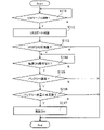
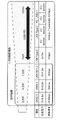
図2は、比較例による主にマイコン11により実行される本体制御部30の起動動作を示すフローチャートである。なお、初期状態においては、撮像装置1の電源はOFFにされており、本体制御部30は動作できない状態とする。
USB PD対応機器の場合、撮像装置1の消費電力以上に電力を供給することができるため、撮像装置1の駆動電力のための給電に加え、充電を行うことができる。
接続機器がPC又はACアダプタの場合、撮像装置1にバッテリー20が装着されている場合は充電を行い、バッテリー20が装着されていない場合充電は行わない。
接続機器がPCの場合、バッテリーが装着されている場合は、MASS接続又はPTP接続、撮像装置1の駆動電力の給電に加えて、余剰の電力で充電を行う。なお、MASS接続は、SDカード等の大容量のデータを転送するための接続である。PTP接続は、画像データを転送するための接続である。
USB PD対応機器でない場合、充電と給電を双方実行するのに十分な電力得られない。よって、充電は、撮像装置の電源がスイッチOFFのときのみ行われる。具体的には以下の通りである。
接続機器がPC又はACアダプタの場合、撮像装置1にバッテリー20が装着されている場合は充電を行い、バッテリー20が装着されていない場合、充電は行わない。
接続機器がPCの場合、バッテリーが装着されている場合は、MASS接続又はPTP接続、及び給電のみ行う。
上記実施の形態1に係る撮像装置1は、バッテリー20を着脱可能な撮像装置であって、CMOSイメージセンサー37と、USBポート16と、マイコン11とを備える。CMOSイメージセンサー37は、被写体を撮像する。USBポート16は、USBケーブルを介して撮像装置1に電力を供給する。マイコン11は、バッテリー20が撮像装置1に装着されているか否かを検出する。マイコン11は、バッテリー20が撮像装置1に装着されている場合、USBポート16からの電力によってCMOSイメージセンサー37の動作を可能にする。マイコン11は、バッテリー20が撮像装置1に装着されていない場合、USBポート16からの電力によってCMOSイメージセンサー37の動作を可能にしない。
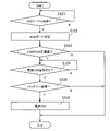
図8は、実施の形態2に係る本体制御部30の起動動作を示すフローチャートである。なお、本実施の形態に係る撮像装置の構成は、図1に示す撮像装置1の構成と同様であるため、説明を省略する。
以上のように、本出願において開示する技術の例示として、各実施の形態を説明した。しかしながら、本開示における技術は、これに限定されず、適宜、変更、置き換え、付加、省略等を行った実施の形態にも適用可能である。また、上記実施の形態で説明した各構成要素を組み合わせて、新たな実施の形態とすることも可能である。
Claims (7)
- バッテリーを着脱可能な撮像装置であって、
被写体を撮像する撮像部と、
USBケーブルを介して前記撮像装置に電力を供給する電力供給端子と、
前記バッテリーが前記撮像装置に装着されているか否かを検出する制御部と
を備え、
前記撮像部は撮像素子を備え、
前記制御部は、
(i)前記バッテリーが前記撮像装置に装着されている場合、前記電力供給端子からの電力によって前記撮像部における前記撮像素子の動作を可能にし、
(ii)前記バッテリーが前記撮像装置に装着されていない場合、前記電力供給端子から前記撮像部における前記撮像素子の動作を賄う電力の供給が可能であっても、前記電力供給端子からの電力による前記撮像部における前記撮像素子の動作を無効にする、
撮像装置。 - 前記制御部は、前記バッテリーが前記撮像装置に装着されている場合、前記バッテリーの残量を検出し、前記バッテリーの残量が前記撮像装置の動作に十分な残量である場合のみ、前記電力供給端子からの電力によって前記撮像部における前記撮像素子の動作を可能にする、
請求項1に記載の撮像装置。 - 前記制御部は、
前記USBケーブルに接続される外部機器がUSB PDの対応機器である場合であって、
(i)前記バッテリーが前記撮像装置に装着されている場合、前記電力供給端子からの電力によって前記撮像部における前記撮像素子の動作を可能にし、
(ii)前記バッテリーが前記撮像装置に装着されていない場合、前記電力供給端子からの電力による前記撮像部における前記撮像素子の動作を可能にしない、
請求項1又は2に記載の撮像装置。 - 前記制御部は、
前記USBケーブルに接続される外部機器がUSB PDの対応機器でない場合、前記バッテリーが前記撮像装置に装着されている場合、前記電力供給端子からの電力による前記撮像部における前記撮像素子の動作を可能とし、前記バッテリーへの充電を禁止する、
請求項3に記載の撮像装置。 - 前記制御部の指令に応じて情報を表示する表示部を備え、
前記表示部は、前記USBケーブルに接続される外部機器がUSB PDの対応機器であるか否かを示す情報を表示する、
請求項1に記載の撮像装置。 - 前記制御部は、前記電力供給端子からの電力によって前記撮像部における前記撮像素子の動作を行っているときに前記バッテリーが取り出されることを検知すると、警告を示す報知を行う、請求項1に記載の撮像装置。
- 前記制御部は、前記バッテリーが前記撮像装置に装着されている場合、電源をONにすることにより、前記撮像部における前記撮像素子の動作を可能にする、
請求項1に記載の撮像装置。
Applications Claiming Priority (3)
| Application Number | Priority Date | Filing Date | Title |
|---|---|---|---|
| JP2018237559 | 2018-12-19 | ||
| JP2018237559 | 2018-12-19 | ||
| PCT/JP2019/033074 WO2020129303A1 (ja) | 2018-12-19 | 2019-08-23 | 撮像装置 |
Publications (2)
| Publication Number | Publication Date |
|---|---|
| JPWO2020129303A1 JPWO2020129303A1 (ja) | 2021-02-15 |
| JP7122590B2 true JP7122590B2 (ja) | 2022-08-22 |
Family
ID=71102779
Family Applications (1)
| Application Number | Title | Priority Date | Filing Date |
|---|---|---|---|
| JP2020520684A Active JP7122590B2 (ja) | 2018-12-19 | 2019-08-23 | 撮像装置 |
Country Status (4)
| Country | Link |
|---|---|
| US (1) | US11265495B2 (ja) |
| EP (1) | EP3699686B1 (ja) |
| JP (1) | JP7122590B2 (ja) |
| WO (1) | WO2020129303A1 (ja) |
Families Citing this family (2)
| Publication number | Priority date | Publication date | Assignee | Title |
|---|---|---|---|---|
| JP7345109B2 (ja) | 2019-08-21 | 2023-09-15 | パナソニックIpマネジメント株式会社 | 撮像装置 |
| TWI818356B (zh) * | 2021-11-16 | 2023-10-11 | 華碩電腦股份有限公司 | 電子裝置及連接裝置 |
Citations (4)
| Publication number | Priority date | Publication date | Assignee | Title |
|---|---|---|---|---|
| JP2001339630A (ja) | 2000-05-25 | 2001-12-07 | Canon Inc | 撮像装置、撮像装置の制御方法、及び媒体 |
| JP2003015782A (ja) | 2001-07-02 | 2003-01-17 | Canon Inc | 電子機器 |
| JP2015007961A (ja) | 2013-05-29 | 2015-01-15 | パナソニックIpマネジメント株式会社 | 電子機器及び撮像装置 |
| JP2018013931A (ja) | 2016-07-20 | 2018-01-25 | キヤノン株式会社 | 電子機器及び電子機器の制御方法 |
Family Cites Families (14)
| Publication number | Priority date | Publication date | Assignee | Title |
|---|---|---|---|---|
| JPH06178452A (ja) | 1992-12-09 | 1994-06-24 | Matsushita Electric Works Ltd | 充交両用電気機器 |
| JP2004227381A (ja) | 2003-01-24 | 2004-08-12 | Matsushita Electric Ind Co Ltd | 情報端末機器 |
| US8040430B2 (en) * | 2003-07-18 | 2011-10-18 | Nikon Corporation | Battery capacity display device and camera |
| JP2005328190A (ja) * | 2004-05-12 | 2005-11-24 | Fuji Photo Film Co Ltd | 監視カメラ |
| EP2051157A1 (en) | 2007-10-15 | 2009-04-22 | Research In Motion Limited | Method and System for Enabling or Disabling Features Based on a Battery Level Threshold |
| US8223262B2 (en) * | 2007-10-26 | 2012-07-17 | Cisco Technology, Inc. | Charging and use scheme for a hand-held electronics device |
| JP5609467B2 (ja) * | 2010-09-15 | 2014-10-22 | 株式会社リコー | 撮像装置及び撮像方法 |
| JP5089789B2 (ja) * | 2011-05-16 | 2012-12-05 | キヤノン株式会社 | 電子機器 |
| JP2013080392A (ja) | 2011-10-04 | 2013-05-02 | Olympus Imaging Corp | 携帯装置のusb充電 |
| JP2013135347A (ja) * | 2011-12-27 | 2013-07-08 | Xacti Corp | 記録装置 |
| JP6797579B2 (ja) * | 2016-07-04 | 2020-12-09 | キヤノン株式会社 | 電子機器、電子機器の制御方法及びプログラム |
| US10476394B2 (en) * | 2016-12-28 | 2019-11-12 | Texas Instruments Incorporated | Dynamic learning of voltage source capabilities |
| JP7130373B2 (ja) * | 2018-01-09 | 2022-09-05 | キヤノン株式会社 | 撮像装置 |
| JP7143173B2 (ja) * | 2018-09-28 | 2022-09-28 | キヤノン株式会社 | 電子機器、制御方法およびプログラム |
-
2019
- 2019-08-23 WO PCT/JP2019/033074 patent/WO2020129303A1/ja unknown
- 2019-08-23 JP JP2020520684A patent/JP7122590B2/ja active Active
- 2019-08-23 EP EP19874764.4A patent/EP3699686B1/en active Active
- 2019-08-23 US US16/766,145 patent/US11265495B2/en active Active
Patent Citations (4)
| Publication number | Priority date | Publication date | Assignee | Title |
|---|---|---|---|---|
| JP2001339630A (ja) | 2000-05-25 | 2001-12-07 | Canon Inc | 撮像装置、撮像装置の制御方法、及び媒体 |
| JP2003015782A (ja) | 2001-07-02 | 2003-01-17 | Canon Inc | 電子機器 |
| JP2015007961A (ja) | 2013-05-29 | 2015-01-15 | パナソニックIpマネジメント株式会社 | 電子機器及び撮像装置 |
| JP2018013931A (ja) | 2016-07-20 | 2018-01-25 | キヤノン株式会社 | 電子機器及び電子機器の制御方法 |
Also Published As
| Publication number | Publication date |
|---|---|
| US20210227161A1 (en) | 2021-07-22 |
| EP3699686A1 (en) | 2020-08-26 |
| US11265495B2 (en) | 2022-03-01 |
| WO2020129303A1 (ja) | 2020-06-25 |
| EP3699686A4 (en) | 2020-11-18 |
| EP3699686B1 (en) | 2022-10-05 |
| JPWO2020129303A1 (ja) | 2021-02-15 |
Similar Documents
| Publication | Publication Date | Title |
|---|---|---|
| US11223734B2 (en) | Information processing apparatus, method of controlling information processing apparatus, and non-transitory computer-readable recording medium | |
| US11239684B2 (en) | Electronic device and control method | |
| US9395781B2 (en) | Electronic device to perform enumeration without power request to an external device when electronic device is on | |
| JP7122590B2 (ja) | 撮像装置 | |
| US11176078B2 (en) | Communication method using input/output interface, and apparatus therefor | |
| US20120210023A1 (en) | Electronic appliance, connecting appliance, electronic appliance system, and computer readable medium | |
| US20160352930A1 (en) | Communication device wirelessly communicating with external device, control method for communication device, and storage medium | |
| US9247135B2 (en) | Electronic device and imaging apparatus | |
| JP5251317B2 (ja) | デバイス機器、ホスト機器及びインターフェイスシステム | |
| JP6754996B1 (ja) | 撮像装置 | |
| JP2013080392A (ja) | 携帯装置のusb充電 | |
| US11622074B2 (en) | Electronic apparatus and accessory system | |
| WO2020129304A1 (ja) | 撮像装置 | |
| WO2020121603A1 (ja) | 撮像装置 | |
| US10277815B2 (en) | Communication apparatus, control method for the communication apparatus, and recording medium | |
| US11431885B2 (en) | Communication apparatus including a communication device for communicating with an external apparatus, and to control in activating the communication device by the communication apparatus and method for controlling the same | |
| WO2014115547A1 (ja) | 電子機器 | |
| JP6746096B2 (ja) | 電力情報管理装置及び電力情報管理方法 | |
| JP6176920B2 (ja) | 電子機器、制御方法及びプログラム | |
| US20190281615A1 (en) | Communication control apparatus and communication control method | |
| JP2019022206A (ja) | 電子機器 | |
| JP2011067068A (ja) | 電子機器及び電源制御方法 | |
| JP2012143021A (ja) | 充電装置 |
Legal Events
| Date | Code | Title | Description |
|---|---|---|---|
| A521 | Request for written amendment filed |
Free format text: JAPANESE INTERMEDIATE CODE: A523 Effective date: 20200410 |
|
| A621 | Written request for application examination |
Free format text: JAPANESE INTERMEDIATE CODE: A621 Effective date: 20200410 |
|
| A131 | Notification of reasons for refusal |
Free format text: JAPANESE INTERMEDIATE CODE: A131 Effective date: 20210309 |
|
| A131 | Notification of reasons for refusal |
Free format text: JAPANESE INTERMEDIATE CODE: A131 Effective date: 20210601 |
|
| A521 | Request for written amendment filed |
Free format text: JAPANESE INTERMEDIATE CODE: A523 Effective date: 20210630 |
|
| A131 | Notification of reasons for refusal |
Free format text: JAPANESE INTERMEDIATE CODE: A131 Effective date: 20211124 |
|
| A521 | Request for written amendment filed |
Free format text: JAPANESE INTERMEDIATE CODE: A523 Effective date: 20211223 |
|
| A131 | Notification of reasons for refusal |
Free format text: JAPANESE INTERMEDIATE CODE: A131 Effective date: 20220510 |
|
| A521 | Request for written amendment filed |
Free format text: JAPANESE INTERMEDIATE CODE: A523 Effective date: 20220607 |
|
| TRDD | Decision of grant or rejection written | ||
| A01 | Written decision to grant a patent or to grant a registration (utility model) |
Free format text: JAPANESE INTERMEDIATE CODE: A01 Effective date: 20220628 |
|
| A61 | First payment of annual fees (during grant procedure) |
Free format text: JAPANESE INTERMEDIATE CODE: A61 Effective date: 20220712 |
|
| R151 | Written notification of patent or utility model registration |
Ref document number: 7122590 Country of ref document: JP Free format text: JAPANESE INTERMEDIATE CODE: R151 |