JP7013630B2 - Optical modulation device - Google Patents
Optical modulation device Download PDFInfo
- Publication number
- JP7013630B2 JP7013630B2 JP2019556618A JP2019556618A JP7013630B2 JP 7013630 B2 JP7013630 B2 JP 7013630B2 JP 2019556618 A JP2019556618 A JP 2019556618A JP 2019556618 A JP2019556618 A JP 2019556618A JP 7013630 B2 JP7013630 B2 JP 7013630B2
- Authority
- JP
- Japan
- Prior art keywords
- polymer film
- degrees
- optical modulation
- layer
- film
- Prior art date
- Legal status (The legal status is an assumption and is not a legal conclusion. Google has not performed a legal analysis and makes no representation as to the accuracy of the status listed.)
- Active
Links
- 230000003287 optical effect Effects 0.000 title claims description 206
- 239000000758 substrate Substances 0.000 claims description 215
- 229920006254 polymer film Polymers 0.000 claims description 128
- 239000004973 liquid crystal related substance Substances 0.000 claims description 90
- 230000005540 biological transmission Effects 0.000 claims description 20
- 239000002245 particle Substances 0.000 claims description 15
- 239000000463 material Substances 0.000 claims description 12
- 101150091203 Acot1 gene Proteins 0.000 claims description 6
- 102100025854 Acyl-coenzyme A thioesterase 1 Human genes 0.000 claims description 6
- 229920006267 polyester film Polymers 0.000 claims description 4
- 238000001962 electrophoresis Methods 0.000 claims description 2
- 239000010410 layer Substances 0.000 description 207
- 239000010408 film Substances 0.000 description 191
- 238000002834 transmittance Methods 0.000 description 50
- 238000000034 method Methods 0.000 description 35
- 239000000975 dye Substances 0.000 description 33
- 150000001875 compounds Chemical class 0.000 description 31
- 239000012071 phase Substances 0.000 description 24
- 229920005989 resin Polymers 0.000 description 23
- 239000011347 resin Substances 0.000 description 23
- 229920000139 polyethylene terephthalate Polymers 0.000 description 19
- 239000005020 polyethylene terephthalate Substances 0.000 description 17
- 229920000642 polymer Polymers 0.000 description 14
- 239000000126 substance Substances 0.000 description 14
- 238000011282 treatment Methods 0.000 description 14
- 229920002799 BoPET Polymers 0.000 description 12
- 238000012360 testing method Methods 0.000 description 12
- 230000000052 comparative effect Effects 0.000 description 11
- 230000010287 polarization Effects 0.000 description 11
- LYCAIKOWRPUZTN-UHFFFAOYSA-N Ethylene glycol Chemical compound OCCO LYCAIKOWRPUZTN-UHFFFAOYSA-N 0.000 description 10
- 238000006243 chemical reaction Methods 0.000 description 10
- 238000010521 absorption reaction Methods 0.000 description 9
- 238000010438 heat treatment Methods 0.000 description 9
- 238000004519 manufacturing process Methods 0.000 description 9
- 230000000704 physical effect Effects 0.000 description 9
- 239000010419 fine particle Substances 0.000 description 8
- 238000005259 measurement Methods 0.000 description 8
- 239000008188 pellet Substances 0.000 description 8
- -1 polyethylene terephthalate Polymers 0.000 description 8
- 238000006116 polymerization reaction Methods 0.000 description 8
- OFOBLEOULBTSOW-UHFFFAOYSA-N Malonic acid Chemical compound OC(=O)CC(O)=O OFOBLEOULBTSOW-UHFFFAOYSA-N 0.000 description 7
- 239000000853 adhesive Substances 0.000 description 7
- 230000001070 adhesive effect Effects 0.000 description 7
- 238000001816 cooling Methods 0.000 description 7
- 150000002009 diols Chemical class 0.000 description 7
- 230000005684 electric field Effects 0.000 description 7
- 230000031700 light absorption Effects 0.000 description 7
- 239000004820 Pressure-sensitive adhesive Substances 0.000 description 6
- KKEYFWRCBNTPAC-UHFFFAOYSA-N Terephthalic acid Chemical compound OC(=O)C1=CC=C(C(O)=O)C=C1 KKEYFWRCBNTPAC-UHFFFAOYSA-N 0.000 description 6
- 238000010586 diagram Methods 0.000 description 6
- 238000011156 evaluation Methods 0.000 description 6
- 239000011521 glass Substances 0.000 description 6
- 239000007788 liquid Substances 0.000 description 6
- 239000002346 layers by function Substances 0.000 description 5
- 239000004417 polycarbonate Substances 0.000 description 5
- 239000011800 void material Substances 0.000 description 5
- 230000000903 blocking effect Effects 0.000 description 4
- 210000004027 cell Anatomy 0.000 description 4
- 239000003795 chemical substances by application Substances 0.000 description 4
- 239000011248 coating agent Substances 0.000 description 4
- 238000000576 coating method Methods 0.000 description 4
- 238000002844 melting Methods 0.000 description 4
- 230000008018 melting Effects 0.000 description 4
- 239000000203 mixture Substances 0.000 description 4
- 239000004642 Polyimide Substances 0.000 description 3
- DNIAPMSPPWPWGF-UHFFFAOYSA-N Propylene glycol Chemical compound CC(O)CO DNIAPMSPPWPWGF-UHFFFAOYSA-N 0.000 description 3
- 239000002253 acid Substances 0.000 description 3
- 239000000654 additive Substances 0.000 description 3
- 239000002216 antistatic agent Substances 0.000 description 3
- 210000002858 crystal cell Anatomy 0.000 description 3
- MTHSVFCYNBDYFN-UHFFFAOYSA-N diethylene glycol Chemical compound OCCOCCO MTHSVFCYNBDYFN-UHFFFAOYSA-N 0.000 description 3
- 230000000694 effects Effects 0.000 description 3
- 150000002148 esters Chemical class 0.000 description 3
- 239000000945 filler Substances 0.000 description 3
- AMGQUBHHOARCQH-UHFFFAOYSA-N indium;oxotin Chemical compound [In].[Sn]=O AMGQUBHHOARCQH-UHFFFAOYSA-N 0.000 description 3
- 229920001721 polyimide Polymers 0.000 description 3
- QPFMBZIOSGYJDE-UHFFFAOYSA-N 1,1,2,2-tetrachloroethane Chemical compound ClC(Cl)C(Cl)Cl QPFMBZIOSGYJDE-UHFFFAOYSA-N 0.000 description 2
- VTYYLEPIZMXCLO-UHFFFAOYSA-L Calcium carbonate Chemical compound [Ca+2].[O-]C([O-])=O VTYYLEPIZMXCLO-UHFFFAOYSA-L 0.000 description 2
- 239000004976 Lyotropic liquid crystal Substances 0.000 description 2
- 239000004743 Polypropylene Substances 0.000 description 2
- VYPSYNLAJGMNEJ-UHFFFAOYSA-N Silicium dioxide Chemical compound O=[Si]=O VYPSYNLAJGMNEJ-UHFFFAOYSA-N 0.000 description 2
- PPBRXRYQALVLMV-UHFFFAOYSA-N Styrene Chemical compound C=CC1=CC=CC=C1 PPBRXRYQALVLMV-UHFFFAOYSA-N 0.000 description 2
- 230000001154 acute effect Effects 0.000 description 2
- WNLRTRBMVRJNCN-UHFFFAOYSA-N adipic acid Chemical compound OC(=O)CCCCC(O)=O WNLRTRBMVRJNCN-UHFFFAOYSA-N 0.000 description 2
- PNEYBMLMFCGWSK-UHFFFAOYSA-N aluminium oxide Inorganic materials [O-2].[O-2].[O-2].[Al+3].[Al+3] PNEYBMLMFCGWSK-UHFFFAOYSA-N 0.000 description 2
- 230000003190 augmentative effect Effects 0.000 description 2
- 239000011230 binding agent Substances 0.000 description 2
- IISBACLAFKSPIT-UHFFFAOYSA-N bisphenol A Chemical compound C=1C=C(O)C=CC=1C(C)(C)C1=CC=C(O)C=C1 IISBACLAFKSPIT-UHFFFAOYSA-N 0.000 description 2
- 239000002131 composite material Substances 0.000 description 2
- 230000001276 controlling effect Effects 0.000 description 2
- 125000004122 cyclic group Chemical group 0.000 description 2
- 230000007547 defect Effects 0.000 description 2
- 239000004744 fabric Substances 0.000 description 2
- 230000009477 glass transition Effects 0.000 description 2
- QQVIHTHCMHWDBS-UHFFFAOYSA-N isophthalic acid Chemical compound OC(=O)C1=CC=CC(C(O)=O)=C1 QQVIHTHCMHWDBS-UHFFFAOYSA-N 0.000 description 2
- 238000002156 mixing Methods 0.000 description 2
- 230000002093 peripheral effect Effects 0.000 description 2
- 239000002685 polymerization catalyst Substances 0.000 description 2
- 239000000047 product Substances 0.000 description 2
- 239000000376 reactant Substances 0.000 description 2
- 239000011342 resin composition Substances 0.000 description 2
- 239000000565 sealant Substances 0.000 description 2
- CXMXRPHRNRROMY-UHFFFAOYSA-N sebacic acid Chemical compound OC(=O)CCCCCCCCC(O)=O CXMXRPHRNRROMY-UHFFFAOYSA-N 0.000 description 2
- 230000035939 shock Effects 0.000 description 2
- 125000006850 spacer group Chemical group 0.000 description 2
- 125000001424 substituent group Chemical group 0.000 description 2
- 239000013638 trimer Substances 0.000 description 2
- PXGZQGDTEZPERC-UHFFFAOYSA-N 1,4-cyclohexanedicarboxylic acid Chemical compound OC(=O)C1CCC(C(O)=O)CC1 PXGZQGDTEZPERC-UHFFFAOYSA-N 0.000 description 1
- LFEWXDOYPCWFHR-UHFFFAOYSA-N 4-(4-carboxybenzoyl)benzoic acid Chemical compound C1=CC(C(=O)O)=CC=C1C(=O)C1=CC=C(C(O)=O)C=C1 LFEWXDOYPCWFHR-UHFFFAOYSA-N 0.000 description 1
- ZCYVEMRRCGMTRW-UHFFFAOYSA-N 7553-56-2 Chemical compound [I] ZCYVEMRRCGMTRW-UHFFFAOYSA-N 0.000 description 1
- 239000005995 Aluminium silicate Substances 0.000 description 1
- 239000004986 Cholesteric liquid crystals (ChLC) Substances 0.000 description 1
- OTMSDBZUPAUEDD-UHFFFAOYSA-N Ethane Chemical compound CC OTMSDBZUPAUEDD-UHFFFAOYSA-N 0.000 description 1
- IAYPIBMASNFSPL-UHFFFAOYSA-N Ethylene oxide Chemical compound C1CO1 IAYPIBMASNFSPL-UHFFFAOYSA-N 0.000 description 1
- VVQNEPGJFQJSBK-UHFFFAOYSA-N Methyl methacrylate Chemical compound COC(=O)C(C)=C VVQNEPGJFQJSBK-UHFFFAOYSA-N 0.000 description 1
- 239000004988 Nematic liquid crystal Substances 0.000 description 1
- ISWSIDIOOBJBQZ-UHFFFAOYSA-N Phenol Chemical compound OC1=CC=CC=C1 ISWSIDIOOBJBQZ-UHFFFAOYSA-N 0.000 description 1
- 239000002202 Polyethylene glycol Substances 0.000 description 1
- 239000004983 Polymer Dispersed Liquid Crystal Substances 0.000 description 1
- 239000004793 Polystyrene Substances 0.000 description 1
- XUIMIQQOPSSXEZ-UHFFFAOYSA-N Silicon Chemical compound [Si] XUIMIQQOPSSXEZ-UHFFFAOYSA-N 0.000 description 1
- 239000004990 Smectic liquid crystal Substances 0.000 description 1
- 229920002125 Sokalan® Polymers 0.000 description 1
- RTAQQCXQSZGOHL-UHFFFAOYSA-N Titanium Chemical compound [Ti] RTAQQCXQSZGOHL-UHFFFAOYSA-N 0.000 description 1
- 125000003647 acryloyl group Chemical group O=C([*])C([H])=C([H])[H] 0.000 description 1
- 230000000996 additive effect Effects 0.000 description 1
- 239000012790 adhesive layer Substances 0.000 description 1
- 239000001361 adipic acid Substances 0.000 description 1
- 235000011037 adipic acid Nutrition 0.000 description 1
- 230000002411 adverse Effects 0.000 description 1
- 229910052782 aluminium Inorganic materials 0.000 description 1
- XAGFODPZIPBFFR-UHFFFAOYSA-N aluminium Chemical compound [Al] XAGFODPZIPBFFR-UHFFFAOYSA-N 0.000 description 1
- 235000012211 aluminium silicate Nutrition 0.000 description 1
- 229910000323 aluminium silicate Inorganic materials 0.000 description 1
- 238000004458 analytical method Methods 0.000 description 1
- 239000001000 anthraquinone dye Substances 0.000 description 1
- 229910052787 antimony Inorganic materials 0.000 description 1
- WATWJIUSRGPENY-UHFFFAOYSA-N antimony atom Chemical compound [Sb] WATWJIUSRGPENY-UHFFFAOYSA-N 0.000 description 1
- 239000003963 antioxidant agent Substances 0.000 description 1
- 230000003078 antioxidant effect Effects 0.000 description 1
- 239000000987 azo dye Substances 0.000 description 1
- 238000005452 bending Methods 0.000 description 1
- 230000015572 biosynthetic process Effects 0.000 description 1
- 239000002981 blocking agent Substances 0.000 description 1
- CDQSJQSWAWPGKG-UHFFFAOYSA-N butane-1,1-diol Chemical compound CCCC(O)O CDQSJQSWAWPGKG-UHFFFAOYSA-N 0.000 description 1
- 229910000019 calcium carbonate Inorganic materials 0.000 description 1
- 239000001506 calcium phosphate Substances 0.000 description 1
- 229910000389 calcium phosphate Inorganic materials 0.000 description 1
- 235000011010 calcium phosphates Nutrition 0.000 description 1
- 239000003054 catalyst Substances 0.000 description 1
- 229920006026 co-polymeric resin Polymers 0.000 description 1
- 239000008119 colloidal silica Substances 0.000 description 1
- 239000013065 commercial product Substances 0.000 description 1
- 238000013329 compounding Methods 0.000 description 1
- 229920001940 conductive polymer Polymers 0.000 description 1
- 238000012790 confirmation Methods 0.000 description 1
- 238000007334 copolymerization reaction Methods 0.000 description 1
- 238000005520 cutting process Methods 0.000 description 1
- PDXRQENMIVHKPI-UHFFFAOYSA-N cyclohexane-1,1-diol Chemical compound OC1(O)CCCCC1 PDXRQENMIVHKPI-UHFFFAOYSA-N 0.000 description 1
- HNPSIPDUKPIQMN-UHFFFAOYSA-N dioxosilane;oxo(oxoalumanyloxy)alumane Chemical compound O=[Si]=O.O=[Al]O[Al]=O HNPSIPDUKPIQMN-UHFFFAOYSA-N 0.000 description 1
- 239000002019 doping agent Substances 0.000 description 1
- 230000009977 dual effect Effects 0.000 description 1
- 238000004043 dyeing Methods 0.000 description 1
- 238000005516 engineering process Methods 0.000 description 1
- RTZKZFJDLAIYFH-UHFFFAOYSA-N ether Substances CCOCC RTZKZFJDLAIYFH-UHFFFAOYSA-N 0.000 description 1
- 238000001125 extrusion Methods 0.000 description 1
- 229910052732 germanium Inorganic materials 0.000 description 1
- GNPVGFCGXDBREM-UHFFFAOYSA-N germanium atom Chemical compound [Ge] GNPVGFCGXDBREM-UHFFFAOYSA-N 0.000 description 1
- 238000009499 grossing Methods 0.000 description 1
- 239000012760 heat stabilizer Substances 0.000 description 1
- WGCNASOHLSPBMP-UHFFFAOYSA-N hydroxyacetaldehyde Natural products OCC=O WGCNASOHLSPBMP-UHFFFAOYSA-N 0.000 description 1
- 230000001771 impaired effect Effects 0.000 description 1
- 238000007689 inspection Methods 0.000 description 1
- 229910052740 iodine Inorganic materials 0.000 description 1
- 239000011630 iodine Substances 0.000 description 1
- 230000001678 irradiating effect Effects 0.000 description 1
- NLYAJNPCOHFWQQ-UHFFFAOYSA-N kaolin Chemical compound O.O.O=[Al]O[Si](=O)O[Si](=O)O[Al]=O NLYAJNPCOHFWQQ-UHFFFAOYSA-N 0.000 description 1
- 238000004898 kneading Methods 0.000 description 1
- 239000000314 lubricant Substances 0.000 description 1
- 230000007257 malfunction Effects 0.000 description 1
- 239000000155 melt Substances 0.000 description 1
- 229910052751 metal Inorganic materials 0.000 description 1
- 239000002184 metal Substances 0.000 description 1
- 229910044991 metal oxide Inorganic materials 0.000 description 1
- 150000004706 metal oxides Chemical class 0.000 description 1
- 239000010445 mica Substances 0.000 description 1
- 229910052618 mica group Inorganic materials 0.000 description 1
- 239000011259 mixed solution Substances 0.000 description 1
- 239000012046 mixed solvent Substances 0.000 description 1
- 239000000178 monomer Substances 0.000 description 1
- 239000002120 nanofilm Substances 0.000 description 1
- 239000002105 nanoparticle Substances 0.000 description 1
- 239000002070 nanowire Substances 0.000 description 1
- SLCVBVWXLSEKPL-UHFFFAOYSA-N neopentyl glycol Chemical compound OCC(C)(C)CO SLCVBVWXLSEKPL-UHFFFAOYSA-N 0.000 description 1
- 238000005192 partition Methods 0.000 description 1
- 229920003229 poly(methyl methacrylate) Polymers 0.000 description 1
- 239000004584 polyacrylic acid Substances 0.000 description 1
- 229920000515 polycarbonate Polymers 0.000 description 1
- 229920006289 polycarbonate film Polymers 0.000 description 1
- 229920001223 polyethylene glycol Polymers 0.000 description 1
- 239000004926 polymethyl methacrylate Substances 0.000 description 1
- 229920001155 polypropylene Polymers 0.000 description 1
- 229920001451 polypropylene glycol Polymers 0.000 description 1
- 229920002223 polystyrene Polymers 0.000 description 1
- 229920002451 polyvinyl alcohol Polymers 0.000 description 1
- 239000002243 precursor Substances 0.000 description 1
- 239000002994 raw material Substances 0.000 description 1
- 238000006479 redox reaction Methods 0.000 description 1
- 230000001105 regulatory effect Effects 0.000 description 1
- 239000010703 silicon Substances 0.000 description 1
- 229910052710 silicon Inorganic materials 0.000 description 1
- 239000000377 silicon dioxide Substances 0.000 description 1
- 239000004984 smart glass Substances 0.000 description 1
- 239000007790 solid phase Substances 0.000 description 1
- 238000005507 spraying Methods 0.000 description 1
- 239000000454 talc Substances 0.000 description 1
- 229910052623 talc Inorganic materials 0.000 description 1
- KKEYFWRCBNTPAC-UHFFFAOYSA-L terephthalate(2-) Chemical compound [O-]C(=O)C1=CC=C(C([O-])=O)C=C1 KKEYFWRCBNTPAC-UHFFFAOYSA-L 0.000 description 1
- 230000000930 thermomechanical effect Effects 0.000 description 1
- 239000010409 thin film Substances 0.000 description 1
- 239000010936 titanium Substances 0.000 description 1
- 229910052719 titanium Inorganic materials 0.000 description 1
- 230000001131 transforming effect Effects 0.000 description 1
- QORWJWZARLRLPR-UHFFFAOYSA-H tricalcium bis(phosphate) Chemical compound [Ca+2].[Ca+2].[Ca+2].[O-]P([O-])([O-])=O.[O-]P([O-])([O-])=O QORWJWZARLRLPR-UHFFFAOYSA-H 0.000 description 1
- 239000006097 ultraviolet radiation absorber Substances 0.000 description 1
- XLYOFNOQVPJJNP-UHFFFAOYSA-N water Substances O XLYOFNOQVPJJNP-UHFFFAOYSA-N 0.000 description 1
- JLYXXMFPNIAWKQ-UHFFFAOYSA-N γ Benzene hexachloride Chemical compound ClC1C(Cl)C(Cl)C(Cl)C(Cl)C1Cl JLYXXMFPNIAWKQ-UHFFFAOYSA-N 0.000 description 1
Images


Classifications
-
- G—PHYSICS
- G02—OPTICS
- G02C—SPECTACLES; SUNGLASSES OR GOGGLES INSOFAR AS THEY HAVE THE SAME FEATURES AS SPECTACLES; CONTACT LENSES
- G02C7/00—Optical parts
- G02C7/10—Filters, e.g. for facilitating adaptation of the eyes to the dark; Sunglasses
- G02C7/101—Filters, e.g. for facilitating adaptation of the eyes to the dark; Sunglasses having an electro-optical light valve
-
- G—PHYSICS
- G02—OPTICS
- G02F—OPTICAL DEVICES OR ARRANGEMENTS FOR THE CONTROL OF LIGHT BY MODIFICATION OF THE OPTICAL PROPERTIES OF THE MEDIA OF THE ELEMENTS INVOLVED THEREIN; NON-LINEAR OPTICS; FREQUENCY-CHANGING OF LIGHT; OPTICAL LOGIC ELEMENTS; OPTICAL ANALOGUE/DIGITAL CONVERTERS
- G02F1/00—Devices or arrangements for the control of the intensity, colour, phase, polarisation or direction of light arriving from an independent light source, e.g. switching, gating or modulating; Non-linear optics
- G02F1/01—Devices or arrangements for the control of the intensity, colour, phase, polarisation or direction of light arriving from an independent light source, e.g. switching, gating or modulating; Non-linear optics for the control of the intensity, phase, polarisation or colour
- G02F1/13—Devices or arrangements for the control of the intensity, colour, phase, polarisation or direction of light arriving from an independent light source, e.g. switching, gating or modulating; Non-linear optics for the control of the intensity, phase, polarisation or colour based on liquid crystals, e.g. single liquid crystal display cells
- G02F1/1326—Liquid crystal optical waveguides or liquid crystal cells specially adapted for gating or modulating between optical waveguides
-
- B—PERFORMING OPERATIONS; TRANSPORTING
- B32—LAYERED PRODUCTS
- B32B—LAYERED PRODUCTS, i.e. PRODUCTS BUILT-UP OF STRATA OF FLAT OR NON-FLAT, e.g. CELLULAR OR HONEYCOMB, FORM
- B32B27/00—Layered products comprising a layer of synthetic resin
- B32B27/06—Layered products comprising a layer of synthetic resin as the main or only constituent of a layer, which is next to another layer of the same or of a different material
-
- B—PERFORMING OPERATIONS; TRANSPORTING
- B32—LAYERED PRODUCTS
- B32B—LAYERED PRODUCTS, i.e. PRODUCTS BUILT-UP OF STRATA OF FLAT OR NON-FLAT, e.g. CELLULAR OR HONEYCOMB, FORM
- B32B7/00—Layered products characterised by the relation between layers; Layered products characterised by the relative orientation of features between layers, or by the relative values of a measurable parameter between layers, i.e. products comprising layers having different physical, chemical or physicochemical properties; Layered products characterised by the interconnection of layers
- B32B7/03—Layered products characterised by the relation between layers; Layered products characterised by the relative orientation of features between layers, or by the relative values of a measurable parameter between layers, i.e. products comprising layers having different physical, chemical or physicochemical properties; Layered products characterised by the interconnection of layers with respect to the orientation of features
- B32B7/035—Layered products characterised by the relation between layers; Layered products characterised by the relative orientation of features between layers, or by the relative values of a measurable parameter between layers, i.e. products comprising layers having different physical, chemical or physicochemical properties; Layered products characterised by the interconnection of layers with respect to the orientation of features using arrangements of stretched films, e.g. of mono-axially stretched films arranged alternately
-
- G—PHYSICS
- G02—OPTICS
- G02B—OPTICAL ELEMENTS, SYSTEMS OR APPARATUS
- G02B27/00—Optical systems or apparatus not provided for by any of the groups G02B1/00 - G02B26/00, G02B30/00
- G02B27/01—Head-up displays
-
- G—PHYSICS
- G02—OPTICS
- G02F—OPTICAL DEVICES OR ARRANGEMENTS FOR THE CONTROL OF LIGHT BY MODIFICATION OF THE OPTICAL PROPERTIES OF THE MEDIA OF THE ELEMENTS INVOLVED THEREIN; NON-LINEAR OPTICS; FREQUENCY-CHANGING OF LIGHT; OPTICAL LOGIC ELEMENTS; OPTICAL ANALOGUE/DIGITAL CONVERTERS
- G02F1/00—Devices or arrangements for the control of the intensity, colour, phase, polarisation or direction of light arriving from an independent light source, e.g. switching, gating or modulating; Non-linear optics
- G02F1/01—Devices or arrangements for the control of the intensity, colour, phase, polarisation or direction of light arriving from an independent light source, e.g. switching, gating or modulating; Non-linear optics for the control of the intensity, phase, polarisation or colour
- G02F1/0102—Constructional details, not otherwise provided for in this subclass
-
- G—PHYSICS
- G02—OPTICS
- G02F—OPTICAL DEVICES OR ARRANGEMENTS FOR THE CONTROL OF LIGHT BY MODIFICATION OF THE OPTICAL PROPERTIES OF THE MEDIA OF THE ELEMENTS INVOLVED THEREIN; NON-LINEAR OPTICS; FREQUENCY-CHANGING OF LIGHT; OPTICAL LOGIC ELEMENTS; OPTICAL ANALOGUE/DIGITAL CONVERTERS
- G02F1/00—Devices or arrangements for the control of the intensity, colour, phase, polarisation or direction of light arriving from an independent light source, e.g. switching, gating or modulating; Non-linear optics
- G02F1/01—Devices or arrangements for the control of the intensity, colour, phase, polarisation or direction of light arriving from an independent light source, e.g. switching, gating or modulating; Non-linear optics for the control of the intensity, phase, polarisation or colour
- G02F1/0126—Opto-optical modulation, i.e. control of one light beam by another light beam, not otherwise provided for in this subclass
-
- G—PHYSICS
- G02—OPTICS
- G02F—OPTICAL DEVICES OR ARRANGEMENTS FOR THE CONTROL OF LIGHT BY MODIFICATION OF THE OPTICAL PROPERTIES OF THE MEDIA OF THE ELEMENTS INVOLVED THEREIN; NON-LINEAR OPTICS; FREQUENCY-CHANGING OF LIGHT; OPTICAL LOGIC ELEMENTS; OPTICAL ANALOGUE/DIGITAL CONVERTERS
- G02F1/00—Devices or arrangements for the control of the intensity, colour, phase, polarisation or direction of light arriving from an independent light source, e.g. switching, gating or modulating; Non-linear optics
- G02F1/01—Devices or arrangements for the control of the intensity, colour, phase, polarisation or direction of light arriving from an independent light source, e.g. switching, gating or modulating; Non-linear optics for the control of the intensity, phase, polarisation or colour
- G02F1/13—Devices or arrangements for the control of the intensity, colour, phase, polarisation or direction of light arriving from an independent light source, e.g. switching, gating or modulating; Non-linear optics for the control of the intensity, phase, polarisation or colour based on liquid crystals, e.g. single liquid crystal display cells
- G02F1/133—Constructional arrangements; Operation of liquid crystal cells; Circuit arrangements
- G02F1/1333—Constructional arrangements; Manufacturing methods
- G02F1/133305—Flexible substrates, e.g. plastics, organic film
-
- G—PHYSICS
- G02—OPTICS
- G02F—OPTICAL DEVICES OR ARRANGEMENTS FOR THE CONTROL OF LIGHT BY MODIFICATION OF THE OPTICAL PROPERTIES OF THE MEDIA OF THE ELEMENTS INVOLVED THEREIN; NON-LINEAR OPTICS; FREQUENCY-CHANGING OF LIGHT; OPTICAL LOGIC ELEMENTS; OPTICAL ANALOGUE/DIGITAL CONVERTERS
- G02F1/00—Devices or arrangements for the control of the intensity, colour, phase, polarisation or direction of light arriving from an independent light source, e.g. switching, gating or modulating; Non-linear optics
- G02F1/01—Devices or arrangements for the control of the intensity, colour, phase, polarisation or direction of light arriving from an independent light source, e.g. switching, gating or modulating; Non-linear optics for the control of the intensity, phase, polarisation or colour
- G02F1/13—Devices or arrangements for the control of the intensity, colour, phase, polarisation or direction of light arriving from an independent light source, e.g. switching, gating or modulating; Non-linear optics for the control of the intensity, phase, polarisation or colour based on liquid crystals, e.g. single liquid crystal display cells
- G02F1/133—Constructional arrangements; Operation of liquid crystal cells; Circuit arrangements
- G02F1/1333—Constructional arrangements; Manufacturing methods
- G02F1/1335—Structural association of cells with optical devices, e.g. polarisers or reflectors
- G02F1/13363—Birefringent elements, e.g. for optical compensation
- G02F1/133631—Birefringent elements, e.g. for optical compensation with a spatial distribution of the retardation value
-
- G—PHYSICS
- G02—OPTICS
- G02F—OPTICAL DEVICES OR ARRANGEMENTS FOR THE CONTROL OF LIGHT BY MODIFICATION OF THE OPTICAL PROPERTIES OF THE MEDIA OF THE ELEMENTS INVOLVED THEREIN; NON-LINEAR OPTICS; FREQUENCY-CHANGING OF LIGHT; OPTICAL LOGIC ELEMENTS; OPTICAL ANALOGUE/DIGITAL CONVERTERS
- G02F1/00—Devices or arrangements for the control of the intensity, colour, phase, polarisation or direction of light arriving from an independent light source, e.g. switching, gating or modulating; Non-linear optics
- G02F1/01—Devices or arrangements for the control of the intensity, colour, phase, polarisation or direction of light arriving from an independent light source, e.g. switching, gating or modulating; Non-linear optics for the control of the intensity, phase, polarisation or colour
- G02F1/13—Devices or arrangements for the control of the intensity, colour, phase, polarisation or direction of light arriving from an independent light source, e.g. switching, gating or modulating; Non-linear optics for the control of the intensity, phase, polarisation or colour based on liquid crystals, e.g. single liquid crystal display cells
- G02F1/133—Constructional arrangements; Operation of liquid crystal cells; Circuit arrangements
- G02F1/1333—Constructional arrangements; Manufacturing methods
- G02F1/1337—Surface-induced orientation of the liquid crystal molecules, e.g. by alignment layers
-
- G—PHYSICS
- G02—OPTICS
- G02F—OPTICAL DEVICES OR ARRANGEMENTS FOR THE CONTROL OF LIGHT BY MODIFICATION OF THE OPTICAL PROPERTIES OF THE MEDIA OF THE ELEMENTS INVOLVED THEREIN; NON-LINEAR OPTICS; FREQUENCY-CHANGING OF LIGHT; OPTICAL LOGIC ELEMENTS; OPTICAL ANALOGUE/DIGITAL CONVERTERS
- G02F1/00—Devices or arrangements for the control of the intensity, colour, phase, polarisation or direction of light arriving from an independent light source, e.g. switching, gating or modulating; Non-linear optics
- G02F1/01—Devices or arrangements for the control of the intensity, colour, phase, polarisation or direction of light arriving from an independent light source, e.g. switching, gating or modulating; Non-linear optics for the control of the intensity, phase, polarisation or colour
- G02F1/13—Devices or arrangements for the control of the intensity, colour, phase, polarisation or direction of light arriving from an independent light source, e.g. switching, gating or modulating; Non-linear optics for the control of the intensity, phase, polarisation or colour based on liquid crystals, e.g. single liquid crystal display cells
- G02F1/133—Constructional arrangements; Operation of liquid crystal cells; Circuit arrangements
- G02F1/1333—Constructional arrangements; Manufacturing methods
- G02F1/1343—Electrodes
- G02F1/134309—Electrodes characterised by their geometrical arrangement
-
- G—PHYSICS
- G02—OPTICS
- G02F—OPTICAL DEVICES OR ARRANGEMENTS FOR THE CONTROL OF LIGHT BY MODIFICATION OF THE OPTICAL PROPERTIES OF THE MEDIA OF THE ELEMENTS INVOLVED THEREIN; NON-LINEAR OPTICS; FREQUENCY-CHANGING OF LIGHT; OPTICAL LOGIC ELEMENTS; OPTICAL ANALOGUE/DIGITAL CONVERTERS
- G02F1/00—Devices or arrangements for the control of the intensity, colour, phase, polarisation or direction of light arriving from an independent light source, e.g. switching, gating or modulating; Non-linear optics
- G02F1/01—Devices or arrangements for the control of the intensity, colour, phase, polarisation or direction of light arriving from an independent light source, e.g. switching, gating or modulating; Non-linear optics for the control of the intensity, phase, polarisation or colour
- G02F1/13—Devices or arrangements for the control of the intensity, colour, phase, polarisation or direction of light arriving from an independent light source, e.g. switching, gating or modulating; Non-linear optics for the control of the intensity, phase, polarisation or colour based on liquid crystals, e.g. single liquid crystal display cells
- G02F1/133—Constructional arrangements; Operation of liquid crystal cells; Circuit arrangements
- G02F1/1333—Constructional arrangements; Manufacturing methods
- G02F1/1347—Arrangement of liquid crystal layers or cells in which the final condition of one light beam is achieved by the addition of the effects of two or more layers or cells
- G02F1/13475—Arrangement of liquid crystal layers or cells in which the final condition of one light beam is achieved by the addition of the effects of two or more layers or cells in which at least one liquid crystal cell or layer is doped with a pleochroic dye, e.g. GH-LC cell
-
- G—PHYSICS
- G02—OPTICS
- G02F—OPTICAL DEVICES OR ARRANGEMENTS FOR THE CONTROL OF LIGHT BY MODIFICATION OF THE OPTICAL PROPERTIES OF THE MEDIA OF THE ELEMENTS INVOLVED THEREIN; NON-LINEAR OPTICS; FREQUENCY-CHANGING OF LIGHT; OPTICAL LOGIC ELEMENTS; OPTICAL ANALOGUE/DIGITAL CONVERTERS
- G02F1/00—Devices or arrangements for the control of the intensity, colour, phase, polarisation or direction of light arriving from an independent light source, e.g. switching, gating or modulating; Non-linear optics
- G02F1/01—Devices or arrangements for the control of the intensity, colour, phase, polarisation or direction of light arriving from an independent light source, e.g. switching, gating or modulating; Non-linear optics for the control of the intensity, phase, polarisation or colour
- G02F1/13—Devices or arrangements for the control of the intensity, colour, phase, polarisation or direction of light arriving from an independent light source, e.g. switching, gating or modulating; Non-linear optics for the control of the intensity, phase, polarisation or colour based on liquid crystals, e.g. single liquid crystal display cells
- G02F1/137—Devices or arrangements for the control of the intensity, colour, phase, polarisation or direction of light arriving from an independent light source, e.g. switching, gating or modulating; Non-linear optics for the control of the intensity, phase, polarisation or colour based on liquid crystals, e.g. single liquid crystal display cells characterised by the electro-optical or magneto-optical effect, e.g. field-induced phase transition, orientation effect, guest-host interaction or dynamic scattering
- G02F1/13725—Devices or arrangements for the control of the intensity, colour, phase, polarisation or direction of light arriving from an independent light source, e.g. switching, gating or modulating; Non-linear optics for the control of the intensity, phase, polarisation or colour based on liquid crystals, e.g. single liquid crystal display cells characterised by the electro-optical or magneto-optical effect, e.g. field-induced phase transition, orientation effect, guest-host interaction or dynamic scattering based on guest-host interaction
-
- G—PHYSICS
- G02—OPTICS
- G02F—OPTICAL DEVICES OR ARRANGEMENTS FOR THE CONTROL OF LIGHT BY MODIFICATION OF THE OPTICAL PROPERTIES OF THE MEDIA OF THE ELEMENTS INVOLVED THEREIN; NON-LINEAR OPTICS; FREQUENCY-CHANGING OF LIGHT; OPTICAL LOGIC ELEMENTS; OPTICAL ANALOGUE/DIGITAL CONVERTERS
- G02F1/00—Devices or arrangements for the control of the intensity, colour, phase, polarisation or direction of light arriving from an independent light source, e.g. switching, gating or modulating; Non-linear optics
- G02F1/01—Devices or arrangements for the control of the intensity, colour, phase, polarisation or direction of light arriving from an independent light source, e.g. switching, gating or modulating; Non-linear optics for the control of the intensity, phase, polarisation or colour
- G02F1/13—Devices or arrangements for the control of the intensity, colour, phase, polarisation or direction of light arriving from an independent light source, e.g. switching, gating or modulating; Non-linear optics for the control of the intensity, phase, polarisation or colour based on liquid crystals, e.g. single liquid crystal display cells
- G02F1/137—Devices or arrangements for the control of the intensity, colour, phase, polarisation or direction of light arriving from an independent light source, e.g. switching, gating or modulating; Non-linear optics for the control of the intensity, phase, polarisation or colour based on liquid crystals, e.g. single liquid crystal display cells characterised by the electro-optical or magneto-optical effect, e.g. field-induced phase transition, orientation effect, guest-host interaction or dynamic scattering
- G02F1/13731—Devices or arrangements for the control of the intensity, colour, phase, polarisation or direction of light arriving from an independent light source, e.g. switching, gating or modulating; Non-linear optics for the control of the intensity, phase, polarisation or colour based on liquid crystals, e.g. single liquid crystal display cells characterised by the electro-optical or magneto-optical effect, e.g. field-induced phase transition, orientation effect, guest-host interaction or dynamic scattering based on a field-induced phase transition
- G02F1/13737—Devices or arrangements for the control of the intensity, colour, phase, polarisation or direction of light arriving from an independent light source, e.g. switching, gating or modulating; Non-linear optics for the control of the intensity, phase, polarisation or colour based on liquid crystals, e.g. single liquid crystal display cells characterised by the electro-optical or magneto-optical effect, e.g. field-induced phase transition, orientation effect, guest-host interaction or dynamic scattering based on a field-induced phase transition in liquid crystals doped with a pleochroic dye
-
- G—PHYSICS
- G02—OPTICS
- G02F—OPTICAL DEVICES OR ARRANGEMENTS FOR THE CONTROL OF LIGHT BY MODIFICATION OF THE OPTICAL PROPERTIES OF THE MEDIA OF THE ELEMENTS INVOLVED THEREIN; NON-LINEAR OPTICS; FREQUENCY-CHANGING OF LIGHT; OPTICAL LOGIC ELEMENTS; OPTICAL ANALOGUE/DIGITAL CONVERTERS
- G02F1/00—Devices or arrangements for the control of the intensity, colour, phase, polarisation or direction of light arriving from an independent light source, e.g. switching, gating or modulating; Non-linear optics
- G02F1/01—Devices or arrangements for the control of the intensity, colour, phase, polarisation or direction of light arriving from an independent light source, e.g. switching, gating or modulating; Non-linear optics for the control of the intensity, phase, polarisation or colour
- G02F1/13—Devices or arrangements for the control of the intensity, colour, phase, polarisation or direction of light arriving from an independent light source, e.g. switching, gating or modulating; Non-linear optics for the control of the intensity, phase, polarisation or colour based on liquid crystals, e.g. single liquid crystal display cells
- G02F1/137—Devices or arrangements for the control of the intensity, colour, phase, polarisation or direction of light arriving from an independent light source, e.g. switching, gating or modulating; Non-linear optics for the control of the intensity, phase, polarisation or colour based on liquid crystals, e.g. single liquid crystal display cells characterised by the electro-optical or magneto-optical effect, e.g. field-induced phase transition, orientation effect, guest-host interaction or dynamic scattering
- G02F1/139—Devices or arrangements for the control of the intensity, colour, phase, polarisation or direction of light arriving from an independent light source, e.g. switching, gating or modulating; Non-linear optics for the control of the intensity, phase, polarisation or colour based on liquid crystals, e.g. single liquid crystal display cells characterised by the electro-optical or magneto-optical effect, e.g. field-induced phase transition, orientation effect, guest-host interaction or dynamic scattering based on orientation effects in which the liquid crystal remains transparent
- G02F1/1396—Devices or arrangements for the control of the intensity, colour, phase, polarisation or direction of light arriving from an independent light source, e.g. switching, gating or modulating; Non-linear optics for the control of the intensity, phase, polarisation or colour based on liquid crystals, e.g. single liquid crystal display cells characterised by the electro-optical or magneto-optical effect, e.g. field-induced phase transition, orientation effect, guest-host interaction or dynamic scattering based on orientation effects in which the liquid crystal remains transparent the liquid crystal being selectively controlled between a twisted state and a non-twisted state, e.g. TN-LC cell
-
- G—PHYSICS
- G02—OPTICS
- G02F—OPTICAL DEVICES OR ARRANGEMENTS FOR THE CONTROL OF LIGHT BY MODIFICATION OF THE OPTICAL PROPERTIES OF THE MEDIA OF THE ELEMENTS INVOLVED THEREIN; NON-LINEAR OPTICS; FREQUENCY-CHANGING OF LIGHT; OPTICAL LOGIC ELEMENTS; OPTICAL ANALOGUE/DIGITAL CONVERTERS
- G02F1/00—Devices or arrangements for the control of the intensity, colour, phase, polarisation or direction of light arriving from an independent light source, e.g. switching, gating or modulating; Non-linear optics
- G02F1/01—Devices or arrangements for the control of the intensity, colour, phase, polarisation or direction of light arriving from an independent light source, e.g. switching, gating or modulating; Non-linear optics for the control of the intensity, phase, polarisation or colour
- G02F1/15—Devices or arrangements for the control of the intensity, colour, phase, polarisation or direction of light arriving from an independent light source, e.g. switching, gating or modulating; Non-linear optics for the control of the intensity, phase, polarisation or colour based on an electrochromic effect
- G02F1/153—Constructional details
-
- B—PERFORMING OPERATIONS; TRANSPORTING
- B32—LAYERED PRODUCTS
- B32B—LAYERED PRODUCTS, i.e. PRODUCTS BUILT-UP OF STRATA OF FLAT OR NON-FLAT, e.g. CELLULAR OR HONEYCOMB, FORM
- B32B2305/00—Condition, form or state of the layers or laminate
- B32B2305/55—Liquid crystals
-
- B—PERFORMING OPERATIONS; TRANSPORTING
- B32—LAYERED PRODUCTS
- B32B—LAYERED PRODUCTS, i.e. PRODUCTS BUILT-UP OF STRATA OF FLAT OR NON-FLAT, e.g. CELLULAR OR HONEYCOMB, FORM
- B32B2307/00—Properties of the layers or laminate
- B32B2307/40—Properties of the layers or laminate having particular optical properties
- B32B2307/402—Coloured
- B32B2307/4026—Coloured within the layer by addition of a colorant, e.g. pigments, dyes
-
- G—PHYSICS
- G02—OPTICS
- G02B—OPTICAL ELEMENTS, SYSTEMS OR APPARATUS
- G02B27/00—Optical systems or apparatus not provided for by any of the groups G02B1/00 - G02B26/00, G02B30/00
- G02B27/01—Head-up displays
- G02B27/0101—Head-up displays characterised by optical features
- G02B2027/0132—Head-up displays characterised by optical features comprising binocular systems
-
- G—PHYSICS
- G02—OPTICS
- G02B—OPTICAL ELEMENTS, SYSTEMS OR APPARATUS
- G02B27/00—Optical systems or apparatus not provided for by any of the groups G02B1/00 - G02B26/00, G02B30/00
- G02B27/01—Head-up displays
- G02B27/017—Head mounted
- G02B2027/0178—Eyeglass type
-
- G—PHYSICS
- G02—OPTICS
- G02B—OPTICAL ELEMENTS, SYSTEMS OR APPARATUS
- G02B27/00—Optical systems or apparatus not provided for by any of the groups G02B1/00 - G02B26/00, G02B30/00
- G02B27/01—Head-up displays
- G02B27/017—Head mounted
- G02B27/0172—Head mounted characterised by optical features
-
- G—PHYSICS
- G02—OPTICS
- G02B—OPTICAL ELEMENTS, SYSTEMS OR APPARATUS
- G02B27/00—Optical systems or apparatus not provided for by any of the groups G02B1/00 - G02B26/00, G02B30/00
- G02B27/01—Head-up displays
- G02B27/017—Head mounted
- G02B27/0176—Head mounted characterised by mechanical features
-
- G—PHYSICS
- G02—OPTICS
- G02C—SPECTACLES; SUNGLASSES OR GOGGLES INSOFAR AS THEY HAVE THE SAME FEATURES AS SPECTACLES; CONTACT LENSES
- G02C2202/00—Generic optical aspects applicable to one or more of the subgroups of G02C7/00
- G02C2202/16—Laminated or compound lenses
-
- G—PHYSICS
- G02—OPTICS
- G02F—OPTICAL DEVICES OR ARRANGEMENTS FOR THE CONTROL OF LIGHT BY MODIFICATION OF THE OPTICAL PROPERTIES OF THE MEDIA OF THE ELEMENTS INVOLVED THEREIN; NON-LINEAR OPTICS; FREQUENCY-CHANGING OF LIGHT; OPTICAL LOGIC ELEMENTS; OPTICAL ANALOGUE/DIGITAL CONVERTERS
- G02F1/00—Devices or arrangements for the control of the intensity, colour, phase, polarisation or direction of light arriving from an independent light source, e.g. switching, gating or modulating; Non-linear optics
- G02F1/01—Devices or arrangements for the control of the intensity, colour, phase, polarisation or direction of light arriving from an independent light source, e.g. switching, gating or modulating; Non-linear optics for the control of the intensity, phase, polarisation or colour
- G02F1/13—Devices or arrangements for the control of the intensity, colour, phase, polarisation or direction of light arriving from an independent light source, e.g. switching, gating or modulating; Non-linear optics for the control of the intensity, phase, polarisation or colour based on liquid crystals, e.g. single liquid crystal display cells
- G02F1/133—Constructional arrangements; Operation of liquid crystal cells; Circuit arrangements
- G02F1/1333—Constructional arrangements; Manufacturing methods
- G02F1/133365—Cells in which the active layer comprises a liquid crystalline polymer
-
- G—PHYSICS
- G02—OPTICS
- G02F—OPTICAL DEVICES OR ARRANGEMENTS FOR THE CONTROL OF LIGHT BY MODIFICATION OF THE OPTICAL PROPERTIES OF THE MEDIA OF THE ELEMENTS INVOLVED THEREIN; NON-LINEAR OPTICS; FREQUENCY-CHANGING OF LIGHT; OPTICAL LOGIC ELEMENTS; OPTICAL ANALOGUE/DIGITAL CONVERTERS
- G02F1/00—Devices or arrangements for the control of the intensity, colour, phase, polarisation or direction of light arriving from an independent light source, e.g. switching, gating or modulating; Non-linear optics
- G02F1/01—Devices or arrangements for the control of the intensity, colour, phase, polarisation or direction of light arriving from an independent light source, e.g. switching, gating or modulating; Non-linear optics for the control of the intensity, phase, polarisation or colour
- G02F1/13—Devices or arrangements for the control of the intensity, colour, phase, polarisation or direction of light arriving from an independent light source, e.g. switching, gating or modulating; Non-linear optics for the control of the intensity, phase, polarisation or colour based on liquid crystals, e.g. single liquid crystal display cells
- G02F1/133—Constructional arrangements; Operation of liquid crystal cells; Circuit arrangements
- G02F1/1333—Constructional arrangements; Manufacturing methods
- G02F1/1335—Structural association of cells with optical devices, e.g. polarisers or reflectors
- G02F1/133528—Polarisers
- G02F1/133536—Reflective polarizers
-
- G—PHYSICS
- G02—OPTICS
- G02F—OPTICAL DEVICES OR ARRANGEMENTS FOR THE CONTROL OF LIGHT BY MODIFICATION OF THE OPTICAL PROPERTIES OF THE MEDIA OF THE ELEMENTS INVOLVED THEREIN; NON-LINEAR OPTICS; FREQUENCY-CHANGING OF LIGHT; OPTICAL LOGIC ELEMENTS; OPTICAL ANALOGUE/DIGITAL CONVERTERS
- G02F1/00—Devices or arrangements for the control of the intensity, colour, phase, polarisation or direction of light arriving from an independent light source, e.g. switching, gating or modulating; Non-linear optics
- G02F1/01—Devices or arrangements for the control of the intensity, colour, phase, polarisation or direction of light arriving from an independent light source, e.g. switching, gating or modulating; Non-linear optics for the control of the intensity, phase, polarisation or colour
- G02F1/13—Devices or arrangements for the control of the intensity, colour, phase, polarisation or direction of light arriving from an independent light source, e.g. switching, gating or modulating; Non-linear optics for the control of the intensity, phase, polarisation or colour based on liquid crystals, e.g. single liquid crystal display cells
- G02F1/133—Constructional arrangements; Operation of liquid crystal cells; Circuit arrangements
- G02F1/1333—Constructional arrangements; Manufacturing methods
- G02F1/1335—Structural association of cells with optical devices, e.g. polarisers or reflectors
- G02F1/133553—Reflecting elements
-
- G—PHYSICS
- G02—OPTICS
- G02F—OPTICAL DEVICES OR ARRANGEMENTS FOR THE CONTROL OF LIGHT BY MODIFICATION OF THE OPTICAL PROPERTIES OF THE MEDIA OF THE ELEMENTS INVOLVED THEREIN; NON-LINEAR OPTICS; FREQUENCY-CHANGING OF LIGHT; OPTICAL LOGIC ELEMENTS; OPTICAL ANALOGUE/DIGITAL CONVERTERS
- G02F1/00—Devices or arrangements for the control of the intensity, colour, phase, polarisation or direction of light arriving from an independent light source, e.g. switching, gating or modulating; Non-linear optics
- G02F1/01—Devices or arrangements for the control of the intensity, colour, phase, polarisation or direction of light arriving from an independent light source, e.g. switching, gating or modulating; Non-linear optics for the control of the intensity, phase, polarisation or colour
- G02F1/13—Devices or arrangements for the control of the intensity, colour, phase, polarisation or direction of light arriving from an independent light source, e.g. switching, gating or modulating; Non-linear optics for the control of the intensity, phase, polarisation or colour based on liquid crystals, e.g. single liquid crystal display cells
- G02F1/133—Constructional arrangements; Operation of liquid crystal cells; Circuit arrangements
- G02F1/1333—Constructional arrangements; Manufacturing methods
- G02F1/1335—Structural association of cells with optical devices, e.g. polarisers or reflectors
- G02F1/13363—Birefringent elements, e.g. for optical compensation
- G02F1/133635—Multifunctional compensators
-
- G—PHYSICS
- G02—OPTICS
- G02F—OPTICAL DEVICES OR ARRANGEMENTS FOR THE CONTROL OF LIGHT BY MODIFICATION OF THE OPTICAL PROPERTIES OF THE MEDIA OF THE ELEMENTS INVOLVED THEREIN; NON-LINEAR OPTICS; FREQUENCY-CHANGING OF LIGHT; OPTICAL LOGIC ELEMENTS; OPTICAL ANALOGUE/DIGITAL CONVERTERS
- G02F1/00—Devices or arrangements for the control of the intensity, colour, phase, polarisation or direction of light arriving from an independent light source, e.g. switching, gating or modulating; Non-linear optics
- G02F1/01—Devices or arrangements for the control of the intensity, colour, phase, polarisation or direction of light arriving from an independent light source, e.g. switching, gating or modulating; Non-linear optics for the control of the intensity, phase, polarisation or colour
- G02F1/13—Devices or arrangements for the control of the intensity, colour, phase, polarisation or direction of light arriving from an independent light source, e.g. switching, gating or modulating; Non-linear optics for the control of the intensity, phase, polarisation or colour based on liquid crystals, e.g. single liquid crystal display cells
- G02F1/133—Constructional arrangements; Operation of liquid crystal cells; Circuit arrangements
- G02F1/1333—Constructional arrangements; Manufacturing methods
- G02F1/1343—Electrodes
- G02F1/13439—Electrodes characterised by their electrical, optical, physical properties; materials therefor; method of making
-
- G—PHYSICS
- G02—OPTICS
- G02F—OPTICAL DEVICES OR ARRANGEMENTS FOR THE CONTROL OF LIGHT BY MODIFICATION OF THE OPTICAL PROPERTIES OF THE MEDIA OF THE ELEMENTS INVOLVED THEREIN; NON-LINEAR OPTICS; FREQUENCY-CHANGING OF LIGHT; OPTICAL LOGIC ELEMENTS; OPTICAL ANALOGUE/DIGITAL CONVERTERS
- G02F1/00—Devices or arrangements for the control of the intensity, colour, phase, polarisation or direction of light arriving from an independent light source, e.g. switching, gating or modulating; Non-linear optics
- G02F1/01—Devices or arrangements for the control of the intensity, colour, phase, polarisation or direction of light arriving from an independent light source, e.g. switching, gating or modulating; Non-linear optics for the control of the intensity, phase, polarisation or colour
- G02F1/13—Devices or arrangements for the control of the intensity, colour, phase, polarisation or direction of light arriving from an independent light source, e.g. switching, gating or modulating; Non-linear optics for the control of the intensity, phase, polarisation or colour based on liquid crystals, e.g. single liquid crystal display cells
- G02F1/133—Constructional arrangements; Operation of liquid crystal cells; Circuit arrangements
- G02F1/1333—Constructional arrangements; Manufacturing methods
- G02F1/1347—Arrangement of liquid crystal layers or cells in which the final condition of one light beam is achieved by the addition of the effects of two or more layers or cells
-
- G—PHYSICS
- G02—OPTICS
- G02F—OPTICAL DEVICES OR ARRANGEMENTS FOR THE CONTROL OF LIGHT BY MODIFICATION OF THE OPTICAL PROPERTIES OF THE MEDIA OF THE ELEMENTS INVOLVED THEREIN; NON-LINEAR OPTICS; FREQUENCY-CHANGING OF LIGHT; OPTICAL LOGIC ELEMENTS; OPTICAL ANALOGUE/DIGITAL CONVERTERS
- G02F2202/00—Materials and properties
- G02F2202/04—Materials and properties dye
-
- G—PHYSICS
- G02—OPTICS
- G02F—OPTICAL DEVICES OR ARRANGEMENTS FOR THE CONTROL OF LIGHT BY MODIFICATION OF THE OPTICAL PROPERTIES OF THE MEDIA OF THE ELEMENTS INVOLVED THEREIN; NON-LINEAR OPTICS; FREQUENCY-CHANGING OF LIGHT; OPTICAL LOGIC ELEMENTS; OPTICAL ANALOGUE/DIGITAL CONVERTERS
- G02F2413/00—Indexing scheme related to G02F1/13363, i.e. to birefringent elements, e.g. for optical compensation, characterised by the number, position, orientation or value of the compensation plates
- G02F2413/01—Number of plates being 1
Description
本出願は、光変調デバイスに関する。 This application relates to an optical modulation device.
本出願は、2017年4月28日付けの韓国特許出願第10-2017-0054964号、2018年1月11月付けの韓国特許出願第10-2018-0003783号、韓国特許出願第10-2018-0003784号、韓国特許出願第10-2018-0003785号、韓国特許出願第10-2018-0003786号、韓国特許出願第10-2018-0003787号、韓国特許出願第10-2018-0003788号、韓国特許出願第10-2018-0003789号、2018年1月12日付けの韓国特許出願第10-2018-0004305号に基づく優先権の利益を主張し、当該韓国特許出願の文献に開示されたすべての内容は、本明細書の一部として含まれる。 This application is based on Korean Patent Application No. 10-2017-0054964 dated April 28, 2017, Korean Patent Application No. 10-2018-0003783 dated January November 2018, Korean Patent Application No. 10-2018- 0003784, Korean Patent Application No. 10-2018-0003785, Korean Patent Application No. 10-2018-0003786, Korean Patent Application No. 10-2018-0003787, Korean Patent Application No. 10-2018-0003788, Korean Patent Application No. 10-2018-0003789, claiming the benefit of priority under Korean Patent Application No. 10-2018-0004305 dated January 12, 2018, all content disclosed in the document of the Korean patent application. , Included as part of this specification.
対向する2つの基板の間に液晶化合物などを含む光変調層を位置させた光変調デバイスは、多様な用途に使用されている。 An optical modulation device in which an optical modulation layer containing a liquid crystal compound or the like is positioned between two opposing substrates is used for various purposes.
例えば、特許文献1(ヨーロッパ公開特許第0022311号)には、液晶ホスト物質(Liquid Crystal Host material)と二色性染料ゲスト(dichroic dye guest)の混合物を適用したいわゆるGHセル(Guest host cell)を光変調層として使用した透過率可変装置が知られている。 For example, in Patent Document 1 (European Publication No. 0022311), a so-called GH cell to which a mixture of a liquid crystal host material and a dichroic dye guest is applied is provided. A variable transmittance device used as an optical modulation layer is known.
このようなデバイスにおいて前記基板としては、主に光学的等方性に優れ、寸法安定性などが良好なガラス基板が使用されてきた。 In such a device, as the substrate, a glass substrate having excellent optical isotropic properties and good dimensional stability has been mainly used.
光変調デバイスの用途が、ディスプレイ装置に限定されず、アイウェアやサンルーフなどのスマートウィンドウなどに拡大され、デバイスの形態も、平面に限定されず、フォールディング(Folding)形態など多様なデザインが適用され、いわゆるフレキシブルデバイスなどの必要性も提起されて、光変調デバイスの基板としてガラス基板の代わりに高分子フィルム基板を適用しようとする試みがある。 The application of optical modulation devices is not limited to display devices, but is expanded to smart windows such as eyewear and sunroofs, and the form of devices is not limited to flat surfaces, and various designs such as folding forms are applied. The need for so-called flexible devices has also been raised, and there is an attempt to apply a polymer film substrate instead of a glass substrate as a substrate for an optical modulation device.
高分子フィルム基板を適用する場合には、ガラス基板と類似した特性を確保するために、できるだけ光学的に等方性であり、いわゆるMD(Machine Direction)およびTD(transverse direction)方向における物性の差異が小さいフィルム基板を適用することが有利であると知られている。 When a polymer film substrate is applied, it is optically isotropic as much as possible in order to secure properties similar to those of a glass substrate, and the difference in physical properties in the so-called MD (Machine Direction) and TD (transverse direction) directions. It is known that it is advantageous to apply a small film substrate.
本出願は、光変調デバイスに関する。本出願では、光学的および機械的に非等方性である高分子フィルムを基板として適用して、機械的物性と光学的物性が共に優れた光変調デバイスを提供することを目的とする。 This application relates to an optical modulation device. An object of the present application is to apply a polymer film which is optically and mechanically anisotropic as a substrate to provide an optical modulation device having excellent mechanical and optical physical properties.
本明細書において角度を定義する用語のうち垂直、平行、直交または水平などは、目的とする効果を損傷させない範囲においての実質的な垂直、平行、直交または水平を意味し、前記垂直、平行、直交または水平の範囲は、製造誤差(error)または偏差(variation)等の誤差を含むものである。例えば、前記それぞれの場合は、約±15度以内の誤差、約±10度以内の誤差または約±5度以内の誤差を含むことができる。 The terms vertical, parallel, orthogonal or horizontal, etc., which define angles herein, mean substantially vertical, parallel, orthogonal or horizontal, as long as they do not impair the desired effect, said vertical, parallel, said. Orthogonal or horizontal ranges include errors such as manufacturing errors (error) or deviations (variation). For example, each of the above cases can include an error within about ± 15 degrees, an error within about ± 10 degrees, or an error within about ± 5 degrees.
本明細書で言及する物性のうち測定温度が当該物性に影響を及ぼす場合、特に別途規定しない限り、前記物性は、常温で測定した物性である。 When the measured temperature affects the physical properties referred to in the present specification, the physical properties are the physical properties measured at room temperature unless otherwise specified.
本明細書で用語「常温」は、特に加温されるか、または減温されない状態における温度であって、約10℃~30℃の範囲内のいずれか一つの温度、例えば、約15℃以上、18℃以上、20℃以上または約23℃以上であり、且つ、約27℃以下の温度を意味する。また、特に別途規定しない限り、本明細書で言及する温度の単位は、℃である。 As used herein, the term "normal temperature" is a temperature that is particularly heated or not cooled, and is any one temperature in the range of about 10 ° C to 30 ° C, for example, about 15 ° C or higher. , 18 ° C. or higher, 20 ° C. or higher, or about 23 ° C. or higher, and means a temperature of about 27 ° C. or lower. Further, unless otherwise specified, the unit of temperature referred to in this specification is ° C.
本明細書で言及する位相差および屈折率は、特に別途規定しない限り、約550nm波長の光に対する屈折率を意味する。 The phase difference and refractive index referred to herein mean the refractive index for light at a wavelength of about 550 nm, unless otherwise specified.
特に別途規定しない限り、本明細書で言及する任意の2つの方向がなす角度は、前記2つの方向がなす鋭角または鈍角のうち鋭角であるか、または時計回りの方向または反時計回りの方向に測定された角度のうち小さい角度であってもよい。したがって、特に別途規定しない限り、本明細書で言及する角度は、正数である。ただし、場合によって、時計回りの方向または反時計回りの方向に測定された角度間の測定方向を表示するために、前記時計回りの方向に測定された角度および反時計回りの方向に測定された角度のうちいずれか一つの角度を正数で表記し、他の一つの角度を負数で表記することもできる。 Unless otherwise specified, the angle formed by any of the two directions referred to herein is the acute or obtuse angle formed by the two directions, or in the clockwise or counterclockwise direction. It may be the smaller of the measured angles. Therefore, unless otherwise specified, the angles referred to herein are positive numbers. However, in some cases, the angle measured in the clockwise direction and the measurement in the counterclockwise direction are measured in order to display the measurement direction between the angles measured in the clockwise direction or the counterclockwise direction. One of the angles can be expressed as a positive number, and the other angle can be expressed as a negative number.
本明細書でアクティブ液晶層または光変調層に含まれる液晶化合物は、液晶分子、液晶ホスト(二色性染料ゲストとともに含まれる場合)または単に液晶と呼称されることもできる。 The liquid crystal compound contained in the active liquid crystal layer or the light modulation layer in the present specification may also be referred to as a liquid crystal molecule, a liquid crystal host (when included together with a dichroic dye guest), or simply a liquid crystal.
本出願は、光変調デバイスに関する。用語「光変調デバイス」は、少なくとも2つ以上の異なる光の状態の間をスイッチングし得るデバイスを意味する。前記で異なる光の状態は、少なくとも透過率および/または反射率が異なる状態を意味する。 This application relates to an optical modulation device. The term "optical modulation device" means a device capable of switching between at least two or more different light states. The different light states mentioned above mean states in which at least the transmittance and / or the reflectance are different.
前記光変調デバイスが具現することができる状態の例としては、透過、遮断、高反射および/または低反射モード状態がある。 Examples of states that the light modulation device can embody include transmission, blocking, high reflection and / or low reflection mode states.
一例において、前記光変調デバイスは、少なくとも前記透過および遮断モード状態の間をスイッチングし得るデバイスであるか、あるいは、前記高反射および低反射モード状態の間をスイッチングし得るデバイスであってもよい。 In one example, the optical modulation device may be at least a device capable of switching between the transmission and cutoff mode states, or a device capable of switching between the high reflection and low reflection mode states.
前記透過モード状態における光変調装置の透過率が少なくとも20%以上、25%以上、30%以上、35%以上、40%以上、45%以上、50%以上、55%以上、60%以上、65%以上、70%以上、75%以上または80%以上程度であってもよい。また、前記遮断モード状態における光変調装置の透過率は、60%以下、55%以下、50%以下、45%以下、40%以下、35%以下、30%以下、25%以下、20%以下、15%以下、10%以下または5%以下であってもよい。透過モードで透過率は、高いほど有利であり、遮断モードでは、透過率が低いほど有利であるので、前記透過モード状態における透過率の上限と遮断モード状態における透過率の下限は、特に制限されず、一例において、前記透過モード状態における透過率の上限は、約100%であり、遮断モード状態における透過率の下限は、約0%であってもよい。 The transmittance of the optical modulator in the transmission mode state is at least 20% or more, 25% or more, 30% or more, 35% or more, 40% or more, 45% or more, 50% or more, 55% or more, 60% or more, 65. It may be about% or more, 70% or more, 75% or more, or 80% or more. The transmittance of the optical modulator in the cutoff mode state is 60% or less, 55% or less, 50% or less, 45% or less, 40% or less, 35% or less, 30% or less, 25% or less, 20% or less. , 15% or less, 10% or less, or 5% or less. The higher the transmittance in the transmission mode, the more advantageous it is, and in the cutoff mode, the lower the transmittance is, the more advantageous it is. Therefore, the upper limit of the transmittance in the transmission mode state and the lower limit of the transmittance in the cutoff mode state are particularly limited. However, in one example, the upper limit of the transmittance in the transmission mode state may be about 100%, and the lower limit of the transmittance in the cutoff mode state may be about 0%.
なお、一例において、前記透過モード状態と遮断モード状態との間をスイッチングし得る光変調デバイスにおいて前記透過モード状態における透過率と遮断モード状態における透過率との差異(透過モード-遮断モード)は、15%以上、20%以上、25%以上、30%以上、35%以上または40%以上であってもよく、90%以下、85%以下、80%以下、75%以下、70%以下、65%以下、60%以下、55%以下、50%以下または45%以下であってもよい。 In one example, in an optical modulation device capable of switching between the transmission mode state and the cutoff mode state, the difference between the transmittance in the transmission mode state and the transmittance in the cutoff mode state (transmission mode-cutoff mode) is It may be 15% or more, 20% or more, 25% or more, 30% or more, 35% or more or 40% or more, 90% or less, 85% or less, 80% or less, 75% or less, 70% or less, 65. It may be% or less, 60% or less, 55% or less, 50% or less, or 45% or less.
前記言及された透過率は、例えば、直進光透過率であってもよい。直進光透過率は、前記デバイスに入射した光に対する前記入射方向と同一方向に透過した光の比率の百分率である。例えば、前記デバイスがフィルムまたはシート形態であれば、前記フィルムまたはシート表面の法線方向に並ぶ方向に入射した光のうちやはり前記法線方向に並ぶ方向に前記デバイスを透過した光の百分率を前記透過率として定義することができる。 The transmittance mentioned above may be, for example, a straight light transmittance. The straight light transmittance is a percentage of the ratio of light transmitted in the same direction as the incident direction to the light incident on the device. For example, if the device is in the form of a film or sheet, the percentage of light transmitted through the device in the direction aligned in the normal direction among the light incident in the direction aligned with the normal direction of the film or sheet surface is calculated. It can be defined as a transmittance.
前記高反射モード状態における光変調装置の反射率は、少なくとも10%以上、15%以上、20%以上、25%以上、30%以上、35%以上または40%以上程度であってもよい。また、前記低反射モード状態において光変調装置の反射率は、20%以下、15%以下、10%以下または5%以下であってもよい。高反射モードで反射率は、高いほど有利であり、低反射モードでは、反射率が低いほど有利であるので、前記高反射モード状態における反射率の上限と低反射モード状態における反射率の下限は、特に制限されず、一例において、前記高反射モード状態における反射率は、60%以下、55%以下または50%以下であってもよく、低反射モード状態における反射率の下限は、約0%であってもよい。 The reflectance of the optical modulator in the high reflection mode state may be at least 10% or more, 15% or more, 20% or more, 25% or more, 30% or more, 35% or more, or 40% or more. Further, in the low reflection mode state, the reflectance of the optical modulator may be 20% or less, 15% or less, 10% or less, or 5% or less. The higher the reflectance in the high reflection mode, the more advantageous it is, and in the low reflection mode, the lower the reflectance, the more advantageous. Therefore, the upper limit of the reflectance in the high reflection mode state and the lower limit of the reflectance in the low reflection mode state are In one example, the reflectance in the high reflection mode state may be 60% or less, 55% or less, or 50% or less, and the lower limit of the reflectance in the low reflection mode state is about 0%. May be.
なお、一例において、前記低反射モード状態と高反射モード状態との間をスイッチングし得る光変調デバイスにおいて前記高反射モード状態における反射率と低反射モード状態における反射率との差異(高反射モード-低反射モード)は、5%以上、10%以上15%以上、20%以上、25%以上、30%以上、35%以上または40%以上であってもよく、90%以下、85%以下、80%以下、75%以下、70%以下、65%以下、60%以下、55%以下、50%以下または45%以下であってもよい。 In one example, in an optical modulation device capable of switching between the low reflection mode state and the high reflection mode state, the difference between the reflectance in the high reflection mode state and the reflectance in the low reflection mode state (high reflection mode-. Low reflection mode) may be 5% or more, 10% or more, 15% or more, 20% or more, 25% or more, 30% or more, 35% or more or 40% or more, 90% or less, 85% or less, It may be 80% or less, 75% or less, 70% or less, 65% or less, 60% or less, 55% or less, 50% or less or 45% or less.
前記言及された透過率および反射率は、それぞれ、可視光領域、例えば、約400~700nmまたは約380~780nmの範囲内のいずれか一つの波長に対する透過率または反射率であるか、前記可視光領域の全体に対する透過率または反射率であるか、前記可視光領域の全体に対する透過率または反射率のうち最大または最小透過率または反射率であるか、または、前記可視光領域内の透過率の平均値または反射率の平均値であってもよい。 The mentioned transmittance and reflectance are, respectively, the transmittance or reflectance for any one wavelength in the visible light region, for example, in the range of about 400 to 700 nm or about 380 to 780 nm, or the visible light. The transmittance or reflectance for the entire region, the maximum or minimum transmittance or reflectance of the entire visible light region, or the transmittance within the visible light region. It may be an average value or an average value of reflectance.
本出願の光変調デバイスは、前記透過モード、遮断モード、高反射モードおよび低反射モード状態から選択されたいずれか一つの状態および他の一つの状態の少なくとも2つ以上の状態の間をスイッチングし得るように設計することができる。必要に応じて、前記状態以外に他の状態、例えば、前記透過モードおよび遮断モード状態の中間透過率の状態、前記高反射モードおよび低反射モード状態の中間反射率の状態などを含むその他第3の状態またはそれ以上の状態も具現することができる。 The optical modulation device of the present application switches between at least two or more states of any one state selected from the transmission mode, cutoff mode, high reflection mode and low reflection mode state and the other state. Can be designed to get. Other third states, including, if necessary, other states other than the above state, for example, the state of the intermediate transmittance in the transmission mode and the cutoff mode state, the state of the intermediate reflectance in the high reflection mode and the low reflection mode state, and the like. The state of or more can also be embodied.
前記のような光変調デバイスのスイッチングは、外部信号の印加、例えば、電圧信号の印加の有無によって調節することができる。例えば、電圧のような外部信号の印加がない状態で光変調デバイスは、前記記述した状態のうちいずれか一つの状態を維持しつつ、電圧が印加されると、他の状態にスイッチングされ得る。印加される電圧の強さ、周波数および/または形態を変更することにより、また、モードの状態を変更したり、あるいは、前記第3の他のモード状態を具現することもできる。 The switching of the optical modulation device as described above can be adjusted by the application of an external signal, for example, the application of a voltage signal. For example, a light modulation device may be switched to another state when a voltage is applied while maintaining any one of the described states in the absence of an external signal such as voltage. By changing the strength, frequency and / or form of the applied voltage, the mode state can also be changed, or the third other mode state can be embodied.
本出願の光変調デバイスは、基本的に対向配置された2つの基板と、前記基板の間に位置する光変調層を有する光変調フィルム層とを含むことができる。以下、便宜上、前記対向配置された2つの基板のうちいずれか一つの基板を第1基板と呼称し、他の基板を第2基板と呼称する。 The optical modulation device of the present application can include two substrates which are basically opposed to each other and an optical modulation film layer having an optical modulation layer located between the substrates. Hereinafter, for convenience, any one of the two boards arranged opposite to each other will be referred to as a first substrate, and the other substrate will be referred to as a second substrate.
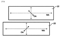
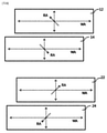
図1は、本出願の例示的な光変調フィルム層の断面図であり、前記光変調フィルム層は、対向配置されている第1および第2基板11、13と、前記第1および第2高分子フィルム基板の間に存在する光変調層12とを含むことができる。
FIG. 1 is a cross-sectional view of an exemplary optical modulation film layer of the present application, wherein the optical modulation film layers are opposed to the first and
本出願の光変調デバイスでは、前記基板として高分子フィルム基板を適用する。前記光変調デバイスの基板は、ガラス層を含まなくてもよい。本出願では、光学的に大きい非等方性を有し、また、機械的物性の側面においても非等方性である高分子フィルム基板を特定の関係で配置することにより、いわゆるレインボー現象などの光学的欠陥がなく、機械的物性に優れたデバイスを構成することができる。このような結果は、優れた光学的物性を確保するためには、光学的に等方性である基板が適用されなければならず、機械的物性が等方性である基板が、デバイスの寸法安定性など機械的物性の側面において有利であるという従来技術の常識に反する結果である。 In the optical modulation device of the present application, a polymer film substrate is applied as the substrate. The substrate of the optical modulation device may not include a glass layer. In this application, the so-called rainbow phenomenon, etc., can be achieved by arranging polymer film substrates that have large optical anisotropy and are also isotropic in terms of mechanical properties in a specific relationship. It is possible to construct a device having no optical defects and excellent mechanical properties. As a result, in order to ensure excellent optical properties, an optically isotropic substrate must be applied, and a substrate having isotropic mechanical properties is the size of the device. This is a result contrary to the conventional wisdom that it is advantageous in terms of mechanical properties such as stability.
本明細書で前記光学的および機械的物性の側面において非等方性である高分子フィルム基板は、非対称基板または非対称高分子フィルム基板と呼称され得る。前記で高分子フィルム基板が光学的に非等方性というのは、前述した面内位相差を有する場合であり、機械的物性の側面において非等方性というのは、後述する物性を有する場合である。 In the present specification, the polymer film substrate which is anisotropic in terms of the optical and mechanical properties may be referred to as an asymmetric substrate or an asymmetric polymer film substrate. In the above, the polymer film substrate is optically anisotropic when it has the above-mentioned in-plane phase difference, and the non-isotropic property in terms of mechanical properties is when it has the physical properties described later. Is.
以下、本明細書で言及する高分子フィルム基板の物性は、前記高分子フィルム基板自体の物性であるか、あるいは、前記高分子フィルム基板の一面に電極層が形成された状態における物性であってもよい。この際、前記電極層は、前記高分子フィルム基板が光学デバイスに含まれている状態で形成されている電極層であってもよい。 Hereinafter, the physical characteristics of the polymer film substrate referred to in the present specification are either the physical characteristics of the polymer film substrate itself or the physical characteristics in a state where an electrode layer is formed on one surface of the polymer film substrate. May be good. At this time, the electrode layer may be an electrode layer formed in a state where the polymer film substrate is included in the optical device.
本明細書で言及する各高分子フィルム基板の物性の測定は、本明細書の実施例の項目に記述した方式によって測定する。 The physical properties of each polymer film substrate referred to in the present specification are measured by the method described in the items of the examples of the present specification.
一例において、前記第1および第2高分子フィルム基板の面内位相差は、それぞれ、約4,000nm以上であってもよい。 In one example, the in-plane phase difference between the first and second polymer film substrates may be about 4,000 nm or more, respectively.
本明細書で面内位相差(Rin)は、下記数式1で計算された値を意味する。 In the present specification, the in-plane phase difference (Rin) means a value calculated by the following formula 1.
[数式1]
Rin=d×(nx-ny)
[Formula 1]
Rin = d × (nx-ny)
数式1で、Rinは、面内位相差であり、dは、高分子フィルム基板の厚さであり、nxは、高分子フィルム基板の遅相軸方向の屈折率であり、nyは、進相軸方向の屈折率であって、前記遅相軸方向と直交する面内方向の屈折率である。 In Equation 1, Rin is the in-plane phase difference, d is the thickness of the polymer film substrate, nx is the refractive index of the polymer film substrate in the slow axis direction, and ny is the phase advance. The refractive index in the axial direction, which is the refractive index in the in-plane direction orthogonal to the slow axis direction.
前記第1および第2高分子フィルム基板の面内位相差は、それぞれ、4,000nm以上、5,000nm以上、6,000nm以上、7,000nm以上、8,000nm以上、9,000nm以上、10,000nm以上、11,000nm以上、12,000nm以上、13,000nm以上、14,000nm以上または15,000nm以上程度であってもよい。また、前記第1および第2高分子フィルム基板のそれぞれの面内位相差は、約50,000nm以下、約40,000nm以下、約30,000nm以下、20,000nm以下、18,000nm以下、16,000nm以下、15,000nm以下または12,000nm以下程度であってもよい。 The in-plane phase differences of the first and second polymer film substrates are 4,000 nm or more, 5,000 nm or more, 6,000 nm or more, 7,000 nm or more, 8,000 nm or more, 9,000 nm or more, and 10 It may be about 000 nm or more, 11,000 nm or more, 12,000 nm or more, 13,000 nm or more, 14,000 nm or more, or 15,000 nm or more. The in-plane phase differences of the first and second polymer film substrates are about 50,000 nm or less, about 40,000 nm or less, about 30,000 nm or less, 20,000 nm or less, 18,000 nm or less, 16 It may be about 000 nm or less, 15,000 nm or less, or 12,000 nm or less.
前記のような大きい位相差を有する高分子フィルムとしては、いわゆる高延伸PET(poly(ethylene terephthalate))フィルムまたはSRF(Super Retardation Film)等と知られているフィルムが代表的に知られている。したがって、本出願で前記高分子フィルム基板は、例えば、ポリエステルフィルム基板であってもよい。 As the polymer film having a large retardation as described above, a so-called high-stretched PET (poly (ethylene terephthalate)) film, an SRF (Super Restriction Film), or the like is typically known. Therefore, in this application, the polymer film substrate may be, for example, a polyester film substrate.
上記のように、極めて高い位相差を有するフィルムは、当業界に公知となっており、このようなフィルムは、光学的に大きい非等方性はもちろん、製造過程においての高延伸などにより機械的物性も大きい非対称性を示す。当業界に公知となった前記高分子フィルム基板の代表的な例としては、PET(poly(ethylene terephthalate))フィルムなどのようなポリエステルフィルムであり、例えば、Toyobo社で供給される商品名SRF(Super Retardation Film)系のフィルムがある。 As described above, films having extremely high phase differences are known in the art, and such films are not only optically large in anisotropy but also mechanically due to high stretching in the manufacturing process. The physical properties also show great asymmetry. A typical example of the polymer film substrate known in the art is a polyester film such as a PET (poly (poly (ethylene terephthalate)) film, for example, a trade name SRF (trade name SRF) supplied by Toyobo. There is a Super Restriction Film) type film.
一例において、前記それぞれの高分子フィルム基板は、面内の任意の第1方向における伸び率E1と前記第1方向と垂直をなす第2方向における伸び率E2との比率E1/E2が3以上であってもよい。前記比率E1/E2は、他の例において、約3.5以上、4以上、4.5以上、5以上、5.5以上、6以上または6.5以上であってもよい。前記比率E1/E2は、他の例において、約20以下、18以下、16以下、14以下、12以下、10以下、8以下または7.5以下であってもよい。 In one example, each of the polymer film substrates has an elongation ratio E1 / E2 of 3 or more between the elongation ratio E1 in any first direction in the plane and the elongation ratio E2 in the second direction perpendicular to the first direction. There may be. In another example, the ratio E1 / E2 may be about 3.5 or more, 4 or more, 4.5 or more, 5 or more, 5.5 or more, 6 or more, or 6.5 or more. In other examples, the ratio E1 / E2 may be about 20 or less, 18 or less, 16 or less, 14 or less, 12 or less, 10 or less, 8 or less, or 7.5 or less.
本明細書で使用する用語「高分子フィルム基板の第1方向、第2方向および第3方向」は、前記フィルム基板の面内の任意の方向である。例えば、高分子フィルム基板が延伸高分子フィルム基板である場合に、前記面内の方向は、前記高分子フィルム基板のMD(Machine Direction)およびTD(transverse direction)方向により形成される面内の方向であってもよい。一例において、本明細書で記述する第1方向は、高分子フィルム基板の遅相軸および進相軸方向のうちいずれか一つの方向であり、第2方向は、遅相軸および進相軸方向のうち他の一つの方向であってもよい。他の例において、前記第1方向は、高分子フィルム基板が延伸高分子フィルム基板である場合に、MD(Machine Direction)およびTD(transverse direction)方向のうちいずれか一つの方向であり、第2方向は、MD(Machine Direction)およびTD(transverse direction)方向のうち他の一つの方向であってもよい。 As used herein, the term "first, second and third directions of a polymer film substrate" is any direction in the plane of the film substrate. For example, when the polymer film substrate is a stretched polymer film substrate, the in-plane direction is an in-plane direction formed by the MD (Machine Direction) and TD (transverse direction) directions of the polymer film substrate. It may be. In one example, the first direction described in the present specification is one of the slow axis and the phase advance axis direction of the polymer film substrate, and the second direction is the slow axis and the phase advance axis direction. It may be in the other one direction. In another example, the first direction is one of the MD (Machine Direction) and TD (transverse direction) directions when the polymer film substrate is a stretched polymer film substrate, and is the second direction. The direction may be one of the MD (Machine Direction) and TD (transverse direction) directions.
一例において、本明細書で言及する高分子フィルム基板の第1方向は、前記TD方向または遅相軸方向であってもよい。 In one example, the first direction of the polymer film substrate referred to herein may be the TD direction or the slow axis direction.
前記で第1および第2高分子フィルム基板のそれぞれの前記第1方向(例えば、前述した遅相軸方向またはTD方向)における伸び率が15%以上または20%以上であってもよい。前記伸び率は、他の例において、約25%以上、30%以上、35%以上または40%以上であってもよく、約60%以下、55%以下、50%以下または45%以下であってもよい。 The elongation rate of the first and second polymer film substrates in the first direction (for example, the slow axis direction or the TD direction described above) may be 15% or more or 20% or more, respectively. In other examples, the elongation may be about 25% or more, 30% or more, 35% or more or 40% or more, and may be about 60% or less, 55% or less, 50% or less or 45% or less. You may.
一例において、前記第1および第2高分子フィルム基板のそれぞれは、前記第1および第2方向とそれぞれ40度~50度の範囲内の角度または約45度をなす第3方向における伸び率E3が、前記第1方向における伸び率E1に比べて大きく、前記第3方向における伸び率E3と前記第2方向における伸び率E2との比率E3/E2が5以上であってもよい。 In one example, each of the first and second polymer film substrates has an elongation rate E3 in the third direction forming an angle within the range of 40 to 50 degrees or about 45 degrees with the first and second directions, respectively. The ratio E3 / E2 between the elongation rate E3 in the third direction and the elongation rate E2 in the second direction may be 5 or more, which is larger than the elongation rate E1 in the first direction.
前記比率E3/E2は、他の例において、5.5以上、6以上、6.5以上、7以上、7.5以上、8以上または8.5以上であってもよく、約20以下、18以下、16以下、14以下、12以下または10以下であってもよい。 In other examples, the ratio E3 / E2 may be 5.5 or more, 6 or more, 6.5 or more, 7 or more, 7.5 or more, 8 or more, or 8.5 or more, and may be about 20 or less. It may be 18 or less, 16 or less, 14 or less, 12 or less, or 10 or less.
第1および第2高分子フィルム基板のそれぞれの前記第3方向における伸び率が30%以上であってもよい。前記伸び率は、他の例において、約35%以上、40%以上、45%以上、50%以上または55%以上であってもよく、約80%以下、75%以下、70%以下または65%以下であってもよい。 The elongation rate of each of the first and second polymer film substrates in the third direction may be 30% or more. In other examples, the elongation may be about 35% or more, 40% or more, 45% or more, 50% or more or 55% or more, and may be about 80% or less, 75% or less, 70% or less or 65. It may be less than or equal to%.
前記第1および第2高分子フィルム基板は、それぞれ、前記第2方向における熱膨張係数CTE2と前記第1方向における熱膨張係数CTE1との比率CTE2/CTE1が1.5以上であってもよい。前記熱膨張係数CTE1、CTE2は、それぞれ、40℃~80℃の温度範囲内で確認される値である。前記比率CTE2/CTE1は、他の例において、約2以上、約2.5以上、3以上または3.5以上であるか、10以下、9以下、8以下、7以下、6以下、5以下または4以下であってもよい。 The first and second polymer film substrates may have a ratio CTE2 / CTE1 of the coefficient of thermal expansion CTE2 in the second direction and the coefficient of thermal expansion CTE1 in the first direction of 1.5 or more, respectively. The coefficients of thermal expansion CTE1 and CTE2 are values confirmed in the temperature range of 40 ° C. to 80 ° C., respectively. In other examples, the ratio CTE2 / CTE1 is about 2 or more, about 2.5 or more, 3 or more or 3.5 or more, or 10 or less, 9 or less, 8 or less, 7 or less, 6 or less, 5 or less. Or it may be 4 or less.
前記第2方向における熱膨張係数CTE2は、5~150ppm/℃の範囲内であってもよい。前記熱膨張係数は、約10ppm/℃以上、15ppm/℃以上、20ppm/℃以上、25ppm/℃以上、30ppm/℃以上、35ppm/℃以上、40ppm/℃以上、45ppm/℃以上、50ppm/℃以上、約55ppm/℃以上、60ppm/℃以上、65ppm/℃以上、70ppm/℃以上、75ppm/℃以上または80ppm/℃以上であるか、140ppm/℃以下、130ppm/℃以下、120ppm/℃以下、100ppm/℃以下、95ppm/℃以下、90ppm/℃以下、85ppm/℃以下、80ppm/℃以下、40ppm/℃以下、30ppm/℃以下または25ppm/℃以下であってもよい。 The coefficient of thermal expansion CTE2 in the second direction may be in the range of 5 to 150 ppm / ° C. The coefficient of thermal expansion is about 10 ppm / ° C or higher, 15 ppm / ° C or higher, 20 ppm / ° C or higher, 25 ppm / ° C or higher, 30 ppm / ° C or higher, 35 ppm / ° C or higher, 40 ppm / ° C or higher, 45 ppm / ° C or higher, 50 ppm / ° C. Above, about 55 ppm / ° C or higher, 60 ppm / ° C or higher, 65 ppm / ° C or higher, 70 ppm / ° C or higher, 75 ppm / ° C or higher or 80 ppm / ° C or higher, 140 ppm / ° C or lower, 130 ppm / ° C or lower, 120 ppm / ° C or lower. , 100 ppm / ° C or lower, 95 ppm / ° C or lower, 90 ppm / ° C or lower, 85 ppm / ° C or lower, 80 ppm / ° C or lower, 40 ppm / ° C or lower, 30 ppm / ° C or lower or 25 ppm / ° C or lower.
前記第1および第2高分子フィルム基板は、それぞれ、前記第2方向における弾性率YM2と前記第1方向における弾性率YM1との比率YM1/YM2が1.5以上であってもよい。前記比率YM1/YM2は、他の例において、約2以上であるか、10以下、9以下、8以下、7以下、6以下、5以下、4以下、3以下または2.5以下であってもよい。 The first and second polymer film substrates may have a ratio YM1 / YM2 of the elastic modulus YM2 in the second direction and the elastic modulus YM1 in the first direction of 1.5 or more, respectively. In other examples, the ratio YM1 / YM2 is about 2 or more, 10 or less, 9 or less, 8 or less, 7 or less, 6 or less, 5 or less, 4 or less, 3 or less, or 2.5 or less. May be good.
前記第1方向における弾性率YM1は、約2~10GPaの範囲内であってもよい。前記弾性率YM1は、他の例において、約2.5GPa以上、3GPa以上、3.5GPa以上、4GPa以上、4.5GPa以上、5GPa以上または5.5GPa以上であるか、約9.5GPa以下、9GPa以下、8.5GPa以下、8GPa以下、7.5GPa以下、7GPa以下、6.5GPa以下または6GPa以下であってもよい。 The elastic modulus YM1 in the first direction may be in the range of about 2 to 10 GPa. In another example, the elastic modulus YM1 is about 2.5 GPa or more, 3 GPa or more, 3.5 GPa or more, 4 GPa or more, 4.5 GPa or more, 5 GPa or more or 5.5 GPa or more, or about 9.5 GPa or less. It may be 9 GPa or less, 8.5 GPa or less, 8 GPa or less, 7.5 GPa or less, 7 GPa or less, 6.5 GPa or less, or 6 GPa or less.
前記弾性率は、いわゆるヤング率(Young's modulus)であり、後述する実施例の方式によって測定する。 The elastic modulus is a so-called Young's modulus, and is measured by the method of Examples described later.
前記第1および第2高分子フィルム基板は、それぞれ、前記第2方向における最大応力MS2と前記第1方向における最大応力MS1との比率MS1/MS2が1.5以上であってもよい。前記比率MS1/MS2は、他の例において、約2以上であるか、10以下、9以下、8以下、7以下、6以下、5以下、4以下、3以下または2.5以下であってもよい。 The ratio MS1 / MS2 of the maximum stress MS2 in the second direction and the maximum stress MS1 in the first direction may be 1.5 or more in the first and second polymer film substrates, respectively. In other examples, the ratio MS1 / MS2 is about 2 or more, or 10 or less, 9 or less, 8 or less, 7 or less, 6 or less, 5 or less, 4 or less, 3 or less, or 2.5 or less. May be good.
前記第1方向(例えば、前述した遅相軸方向またはTD方向)における最大応力MS1は、約80~300MPaの範囲内であってもよい。前記最大応力MS1は、他の例において、約90MPa以上、約100MPa以上、約110MPa以上、約120MPa以上、約130MPa以上、約140MPa以上、約150MPa以上、約155MPa以上、160MPa以上、165MPa以上、170MPa以上、175MPa以上または180MPa以上であるか、約300MPa以下、約290MPa以下、約280MPa以下、約270MPa以下、約260MPa以下、約250MPa以下、約245MPa以下、240MPa以下、235MPa以下、230MPa以下、225MPa以下、220MPa以下、215MPa以下、210MPa以下、205MPa以下、200MPa以下、195MPa以下または190MPa以下であってもよい。 The maximum stress MS1 in the first direction (for example, the slow axis direction or the TD direction described above) may be in the range of about 80 to 300 MPa. In another example, the maximum stress MS1 is about 90 MPa or more, about 100 MPa or more, about 110 MPa or more, about 120 MPa or more, about 130 MPa or more, about 140 MPa or more, about 150 MPa or more, about 155 MPa or more, 160 MPa or more, 165 MPa or more, 170 MPa. Above, 175 MPa or more or 180 MPa or more, about 300 MPa or less, about 290 MPa or less, about 280 MPa or less, about 270 MPa or less, about 260 MPa or less, about 250 MPa or less, about 245 MPa or less, 240 MPa or less, 235 MPa or less, 230 MPa or less, 225 MPa or less. , 220 MPa or less, 215 MPa or less, 210 MPa or less, 205 MPa or less, 200 MPa or less, 195 MPa or less, or 190 MPa or less.
本出願の光変調デバイスにおいて前記第1高分子フィルム基板の第1方向と前記第2高分子フィルム基板の第1方向とのなす角度の絶対値は、0度~10度または0度~5度の範囲内であるか、あるいは、前記第1方向は、略互いに水平であってもよい。前記第1方向は、前述したように、高分子フィルム基板の遅相軸方向またはTD方向であってもよい。 In the optical modulation device of the present application, the absolute value of the angle formed by the first direction of the first polymer film substrate and the first direction of the second polymer film substrate is 0 degrees to 10 degrees or 0 degrees to 5 degrees. Or the first direction may be approximately horizontal to each other. As described above, the first direction may be the slow axis direction or the TD direction of the polymer film substrate.
本出願では、上記のように、光学的および機械的物性が非対称性である高分子フィルム基板を前記のような特定の関係を有するように配置してデバイスを構成することにより、光学的物性および機械的物性を良好に具現することができる。 In the present application, as described above, the polymer film substrate having asymmetric optical and mechanical properties is arranged so as to have the specific relationship as described above to configure the device, thereby performing the optical properties and the optical properties. The mechanical properties can be well embodied.
このような効果が具現される理由は、明確ではないが、少なくとも2つの高分子フィルム基板が有する大きい非対称性を類似に調節し、さらに前記両者の非対称を特定の軸を基準として対称を成すように配置することにより、等方性構造のフィルムの適用時に比べて、さらに優れた光学的および機械的物性のバランスが確保されるからであると推測される。 The reason why such an effect is realized is not clear, but the large asymmetry of at least two polymer film substrates should be adjusted similarly, and the asymmetry of the two should be made symmetrical with respect to a specific axis. It is presumed that the arrangement in the above ensures a better balance of optical and mechanical properties as compared with the case of applying a film having an isotropic structure.
前述したように、前記のような大きい光学的および機械的非対称性を有する高分子フィルムの代表的な例は、いわゆる高延伸ポリエステルフィルム等と知られた延伸PET(polyethyleneterephtalate)フィルムであり、このようなフィルムは、当業界で容易に入手することができる。 As described above, a typical example of a polymer film having large optical and mechanical asymmetry as described above is a stretched PET (polyethylene terephthalate) film known as a so-called highly stretched polyester film or the like. Films are readily available in the industry.
通常、延伸PETフィルムは、PET系樹脂を溶融/押出で製膜し、延伸して製造した1層以上の一軸延伸フィルムまたは製膜後に縦および横延伸して製造した1層以上の二軸延伸フィルムである。 Usually, a stretched PET film is a uniaxially stretched film having one or more layers produced by melting / extruding a PET resin and stretching it, or a biaxially stretched film having one or more layers produced by longitudinally and transversely stretching after film formation. It is a film.
PET系樹脂は、通常、反復単位の80モル%以上がエチレンテレフタレートからなる樹脂を意味し、他のジカルボン酸成分とジオール成分を含むこともできる。他のジカルボン酸成分としては、特に限定されるものではないが、例えばイソフタル酸、p-ベータ-オキシエトキシ安息香酸、4,4'-ジカルボキシジフェニル、4,4'-ジカルボキシベンゾフェノン、ビス(4-カルボキシフェニル)エタン、アジピン酸、セバシン酸および/または1,4-ジカルボキシシクロヘキサンなどが挙げられる。 The PET-based resin usually means a resin in which 80 mol% or more of the repeating unit is composed of polyethylene terephthalate, and may also contain other dicarboxylic acid components and diol components. The other dicarboxylic acid components are not particularly limited, but are, for example, isophthalic acid, p-beta-oxyethoxybenzoic acid, 4,4'-dicarboxydiphenyl, 4,4'-dicarboxybenzophenone, and bis (. 4-carboxyphenyl) ethane, adipic acid, sebacic acid and / or 1,4-dicarboxycyclohexane and the like.
他のジオール成分としては、特に限定されるものではないが、プロピレングリコール、ブタンジオール、ネオペンチルグリコール、ジエチレングリコール、シクロヘキサンジオール、ビスフェノールAのエチレンオキシド付加物、ポリエチレングリコール、ポリプロピレングリコールおよび/またはポリテトラメチレングリコールなどが挙げられる。 Other diol components are not particularly limited, but are not limited to propylene glycol, butanediol, neopentyl glycol, diethylene glycol, cyclohexanediol, ethylene oxide adduct of bisphenol A, polyethylene glycol, polypropylene glycol and / or polytetramethylene glycol. And so on.
前記ジカルボン酸成分やジオール成分は、必要に応じて2種以上を組み合わせて使用することができる。また、p-オキシ安息香酸などのオキシカルボン酸を併用することもできる。また、他の共重合成分として、少量のアミド結合、ウレタン結合、エーテル結合およびカルボネート結合などを含有するジカルボン酸成分、またはジオール成分が使用されることもできる。 The dicarboxylic acid component and the diol component can be used in combination of two or more, if necessary. In addition, an oxycarboxylic acid such as p-oxybenzoic acid can also be used in combination. Further, as the other copolymerization component, a dicarboxylic acid component containing a small amount of amide bond, urethane bond, ether bond, carbonate bond and the like, or a diol component can also be used.
PET系樹脂の製造方法としては、テレフタル酸、エチレングリコールおよび/または必要に応じて他のジカルボン酸または他のジオールを直接重縮合させる方法、テレフタル酸のジアルキルエステルおよびエチレングリコールおよび/または必要に応じて他のジカルボン酸のジアルキルエステルまたは他のジオールをエステル交換反応させた後に重縮合させる方法、およびテレフタル酸および/または必要に応じて他のジカルボン酸のエチレングリコールエステルおよび/または必要に応じて他のジオールエステルを重縮合させる方法などが採用される。 As a method for producing a PET-based resin, a method of directly polycondensing terephthalic acid, ethylene glycol and / or other dicarboxylic acid or other diol as required, a dialkyl ester of terephthalic acid and ethylene glycol and / or as required A method in which a dialkyl ester of another dicarboxylic acid or another diol is subjected to an ester exchange reaction and then polycondensed, and an ethylene glycol ester of a terephthalic acid and / or another dicarboxylic acid and / or, if necessary, the other. A method of polycondensing the diol ester of the above is adopted.
それぞれの重合反応には、アンチモン系、チタン系、ゲルマニウム系またはアルミニウム系化合物を含む重合触媒、または、前記複合化合物を含む重合触媒が使用できる。 For each polymerization reaction, a polymerization catalyst containing an antimony-based, titanium-based, germanium-based or aluminum-based compound, or a polymerization catalyst containing the composite compound can be used.
重合反応条件は、使用される単量体、触媒、反応装置および目的とする樹脂物性によって適宜選択することができ、特に制限されるものではないが、例えば反応温度は、通常、約150℃~約300℃、約200℃~約300℃または約260℃~約300℃である。また、反応圧力は、通常、大気圧~約2.7Paであり、反応の後半には、減圧側であってもよい。 The polymerization reaction conditions can be appropriately selected depending on the monomer used, the catalyst, the reaction apparatus and the physical characteristics of the target resin, and are not particularly limited. For example, the reaction temperature is usually about 150 ° C. to higher. It is about 300 ° C., about 200 ° C. to about 300 ° C. or about 260 ° C. to about 300 ° C. The reaction pressure is usually from atmospheric pressure to about 2.7 Pa, and may be on the reduced pressure side in the latter half of the reaction.
重合反応は、ジオール、アルキル化合物または水などの離脱反応物を揮発させることにより進行される。 The polymerization reaction proceeds by volatilizing a withdrawal reactant such as a diol, an alkyl compound or water.
重合装置は、反応槽が一つに完結されるものであってもよく、または複数の反応槽を連結したものであってもよい。この場合、通常、重合度によって反応物は反応槽の間を移送されながら重合される。また、重合の後半に、横型反応装置を備え、加熱/混練しつつ揮発させる方法も採用することができる。 The polymerization apparatus may be one in which the reaction tanks are completed in one, or may be one in which a plurality of reaction tanks are connected. In this case, the reactants are usually polymerized while being transferred between the reaction tanks depending on the degree of polymerization. Further, a method of providing a horizontal reaction device in the latter half of the polymerization and volatilizing while heating / kneading can also be adopted.
重合終了後の樹脂は、溶融状態で反応槽や横型反応装置から放出された後、冷却ドラムや冷却ベルトなどで冷却・粉砕されたフレーク状の形態で、または押出器に導入されてひも形状に押出された後にカットされたペレット状の形態で得られる。また、必要に応じて固相重合を行って、分子量を向上させるか、または低分子量の成分を減少させることもできる。PET系樹脂に含まれ得る低分子量の成分としては、環状の三量体成分が挙げられるが、このような環状の三量体成分の樹脂中においての含有量は、通常、5000ppm以下または3000ppm以下に調節される。 After the polymerization is completed, the resin is discharged from the reaction tank or horizontal reactor in a molten state, and then cooled and crushed by a cooling drum or a cooling belt in the form of flakes, or introduced into an extruder to form a string. It is obtained in the form of pellets that have been extruded and then cut. Further, if necessary, solid phase polymerization can be carried out to increase the molecular weight or reduce the components having a low molecular weight. Examples of the low molecular weight component that can be contained in the PET-based resin include a cyclic trimer component, and the content of such a cyclic trimer component in the resin is usually 5000 ppm or less or 3000 ppm or less. Is adjusted to.
PET系樹脂の分子量は、フェノール/テトラクロロエタン=50/50(重量比)の混合溶媒に樹脂を溶解させ、30℃で測定した極限粘度で示したとき、通常、0.45~1.0dL/g、0.50~10dL/gまたは0.52~0.80dL/gの範囲である。 The molecular weight of the PET-based resin is usually 0.45 to 1.0 dL / when the resin is dissolved in a mixed solvent of phenol / tetrachloroethane = 50/50 (weight ratio) and shown by the extreme viscosity measured at 30 ° C. It is in the range of g, 0.50 to 10 dL / g or 0.52 to 0.80 dL / g.
また、PET系樹脂は、必要に応じて添加剤を含有することができる。添加剤としては、例えば潤滑剤、ブロッキング防止剤、熱安定剤、酸化防止剤、帯電防止剤、耐光剤および耐衝撃性改良剤などが挙げられる。その添加量は、光学物性に悪影響を及ぼさない範囲とすることが好ましい。 In addition, the PET-based resin can contain additives as needed. Examples of the additive include a lubricant, an antiblocking agent, a heat stabilizer, an antioxidant, an antistatic agent, a light resistant agent, an impact resistance improving agent and the like. The amount added is preferably in a range that does not adversely affect the optical characteristics.
PET系樹脂は、このような添加剤の配合のために、および後述するフィルム成形のために、通常、押出器により組み立てられたペレット形状で用いられる。ペレットのサイズや形状は、特に制限されるものではないが、通常、高さ、直径がいずれも5mm以下である円周状、球状または扁平球状である。このようにして得られるPET系樹脂は、フィルム状に成形し、延伸処理することにより、透明で且つ均質の機械的強度が高いPETフィルムとすることができる。その製造方法としては、特に限定されるものではないが、例えば下記に記載する方法が採用される。 PET-based resins are usually used in pellet form assembled by an extruder for compounding such additives and for film forming as described below. The size and shape of the pellets are not particularly limited, but are usually circumferential, spherical or flat spherical having a height and a diameter of 5 mm or less. The PET-based resin thus obtained can be formed into a film and stretched to obtain a transparent and homogeneous PET film having high mechanical strength. The manufacturing method is not particularly limited, but for example, the method described below is adopted.
乾燥させたPET樹脂からなるペレットを溶融押出装置に供給し、融点以上で加熱して溶融させる。次に、溶融した樹脂をダイから押出、回転冷却ドラム上でガラス転移温度以下の温度となるように、急冷固化させて、実質的に非結晶状態の未延伸フィルムを得る。この溶融温度は、使用されるPET系樹脂の融点や押出器によって定められるものであり、特に制限されるものではないが、通常、250℃~350℃である。また、フィルムの平面性を向上させるためには、フィルムと回転冷却ドラムとの密着性を高めることが好ましく、静電印加密着法または液体塗布密着法が好ましく採用される。静電印加密着法とは、通常、フィルムの上面側にフィルムの流れと直交する方向に線状電極を設置し、該電極に約5~10kVの直流電圧を印加することにより、フィルムに正電荷を提供して、回転冷却ドラムとフィルムとの密着性を向上させる方法である。また、液体塗布密着法とは、回転冷却ドラム表面の全体または一部(例えば、フィルムの両端部と接触する部分のみ)に液体を均一に塗布することにより、回転冷却ドラムとフィルムとの密着性を向上させる方法である。必要に応じて両者を併用することもできる。使用されるPET系樹脂は、必要に応じて2種以上の樹脂、構造や組成が異なる樹脂を混合することもできる。例えば、ブロッキング防止剤としての粒状充填材、紫外線吸収剤または帯電防止剤などが配合されたペレットと、無配合のペレットを混合して利用することなどが挙げられる。 Pellets made of dried PET resin are supplied to a melt extruder and heated above the melting point to be melted. Next, the molten resin is extruded from a die and rapidly cooled and solidified on a rotary cooling drum so as to have a temperature equal to or lower than the glass transition temperature to obtain an unstretched film in a substantially amorphous state. This melting temperature is determined by the melting point of the PET resin used and the extruder, and is not particularly limited, but is usually 250 ° C to 350 ° C. Further, in order to improve the flatness of the film, it is preferable to improve the adhesion between the film and the rotary cooling drum, and the electrostatic application adhesion method or the liquid coating adhesion method is preferably adopted. In the electrostatic application close contact method, a linear electrode is usually installed on the upper surface side of the film in a direction orthogonal to the flow of the film, and a DC voltage of about 5 to 10 kV is applied to the electrode to charge the film with a positive charge. Is a method of improving the adhesion between the rotary cooling drum and the film. In addition, the liquid application adhesion method is the adhesion between the rotary cooling drum and the film by uniformly applying the liquid to the entire or part of the surface of the rotary cooling drum (for example, only the portion in contact with both ends of the film). Is a way to improve. Both can be used together if necessary. As the PET-based resin used, two or more kinds of resins and resins having different structures and compositions can be mixed, if necessary. For example, pellets containing a granular filler as an antiblocking agent, an ultraviolet absorber, an antistatic agent, or the like and pellets containing no antistatic agent may be mixed and used.
また、押出させるフィルムの積層数は、必要に応じて2層以上とすることもできる。例えば、ブロッキング防止剤としての粒状充填材を配合したペレットと無配合のペレットを用意し、他の押出器から同じダイに供給して、「充填材配合/無配合/充填材配合」の2種の3層からなるフィルムを押出させることなどが挙げられる。 Further, the number of laminated films to be extruded may be two or more, if necessary. For example, pellets containing a granular filler as an anti-blocking agent and pellets containing no filler are prepared and supplied to the same die from another extruder, and there are two types of "filler-blended / non-blended / filler-blended". For example, extruding a film composed of three layers of the above.
前記未延伸フィルムは、ガラス転移温度以上の温度で通常、まず押出方向に縦延伸される。延伸温度は、通常、70℃~150℃、80~130℃または90~120℃である。また、延伸倍率は、通常、1.1~6倍または2~5.5倍である。延伸は、1回済み、または必要に応じて複数回に分けて行うこともできる。 The unstretched film is usually first longitudinally stretched in the extrusion direction at a temperature equal to or higher than the glass transition temperature. The stretching temperature is usually 70 ° C. to 150 ° C., 80 to 130 ° C. or 90 to 120 ° C. The draw ratio is usually 1.1 to 6 times or 2 to 5.5 times. The stretching may be performed once, or may be divided into a plurality of times as required.
このようにして得られる縦延伸フィルムは、以後に熱処理を行うことができる。次に、必要に応じて弛緩処理を行うこともできる。この熱処理温度は、通常、150℃~250℃、180~245℃または200~230℃である。また、熱処理時間は、通常、1~600秒間または1~300秒間または1~60秒間である。 The vertically stretched film thus obtained can be subsequently heat-treated. Next, relaxation treatment can be performed as needed. The heat treatment temperature is usually 150 ° C. to 250 ° C., 180 to 245 ° C. or 200 to 230 ° C. The heat treatment time is usually 1 to 600 seconds, 1 to 300 seconds, or 1 to 60 seconds.
弛緩処理の温度は、通常、90~200℃または120~180℃である。また、弛緩量は、通常、0.1~20%または2~5%である。この弛緩処理の温度および弛緩量は、弛緩処理後のPETフィルムの150℃での熱収縮率が2%以下となるように、弛緩量および弛緩処理時の温度を設定することができる。 The temperature of the relaxation treatment is usually 90 to 200 ° C or 120 to 180 ° C. The amount of relaxation is usually 0.1 to 20% or 2 to 5%. The temperature and the relaxation amount of the relaxation treatment can be set to the relaxation amount and the temperature at the time of the relaxation treatment so that the heat shrinkage rate of the PET film after the relaxation treatment at 150 ° C. is 2% or less.
一軸延伸および二軸延伸フィルムを得る場合、通常、縦延伸処理後に、または必要に応じて熱処理または弛緩処理を経た後に、テンターにより横延伸が行われる。この延伸温度は、通常、70℃~150℃、80℃~130℃または90℃~120℃である。また、延伸倍率は、通常、1.1~6倍または2~5.5倍である。その後、熱処理および必要に応じて弛緩処理を行うことができる。熱処理温度は、通常、150℃~250℃または180℃~245℃または200~230℃である。熱処理時間は、通常、1~600秒間、1~300秒間または1~60秒間である。 When uniaxially stretched and biaxially stretched films are obtained, transverse stretching is usually performed by a tenter after a longitudinal stretching treatment or, if necessary, a heat treatment or a relaxation treatment. The stretching temperature is usually 70 ° C. to 150 ° C., 80 ° C. to 130 ° C. or 90 ° C. to 120 ° C. The draw ratio is usually 1.1 to 6 times or 2 to 5.5 times. After that, heat treatment and relaxation treatment can be performed if necessary. The heat treatment temperature is usually 150 ° C. to 250 ° C. or 180 ° C. to 245 ° C. or 200 to 230 ° C. The heat treatment time is usually 1 to 600 seconds, 1 to 300 seconds or 1 to 60 seconds.
弛緩処理の温度は、通常、100~230℃、110~210℃または120~180℃である。また、弛緩量は、通常、01~20%、1~10%または2~5%である。この弛緩処理の温度および弛緩量は、弛緩処理後のPETフィルムの150℃での熱収縮率が2%以下となるように、その弛緩量および弛緩処理時の温度を設定することができる。 The temperature of the relaxation treatment is usually 100 to 230 ° C, 110 to 210 ° C or 120 to 180 ° C. The amount of relaxation is usually 01 to 20%, 1 to 10% or 2 to 5%. The temperature and the relaxation amount of the relaxation treatment can be set so that the heat shrinkage rate of the PET film after the relaxation treatment at 150 ° C. is 2% or less.
一軸延伸および二軸延伸処理においては、横延伸後、ボーイングと代表されるような配向主軸の変形を緩和させるために、再度熱処理を行うか、または延伸処理を行うことができる。ボーイングによる配向主軸の延伸方向に対する変形の最大値は、通常、45度以内、30度以内または15度以内である。また、ここで、延伸方向とは、縦延伸または横延伸における延伸が大きい方向をいう。 In the uniaxial stretching and biaxial stretching treatments, after the transverse stretching, the heat treatment may be performed again or the stretching treatment may be performed in order to alleviate the deformation of the orientation spindle as typified by Boeing. The maximum value of deformation of the orientation spindle in the stretching direction by Boeing is usually within 45 degrees, within 30 degrees, or within 15 degrees. Further, here, the stretching direction means a direction in which stretching in longitudinal stretching or transverse stretching is large.
PETフィルムの二軸延伸では、通常、横延伸倍率の場合が縦延伸倍率より若干大きく行われ、この場合、延伸方向とは、前記フィルムの長さ方向に対して垂直方向をいう。また、一軸延伸では、通常、上記したように、横方向に延伸され、この場合、延伸方向とは、同一に長さ方向に対して垂直方向をいう。 In the biaxial stretching of the PET film, the transverse stretching ratio is usually slightly larger than the longitudinal stretching ratio, and in this case, the stretching direction means the direction perpendicular to the length direction of the film. Further, in uniaxial stretching, as described above, it is usually stretched in the lateral direction, and in this case, the stretching direction is the same as the direction perpendicular to the length direction.
また、配向主軸とは、延伸PETフィルム上の任意の点での分子配向方向をいう。また、配向主軸の延伸方向に対する変形とは、配向主軸と延伸方向との角度差をいう。また、その最大値とは、長さ方向に対して垂直方向上での値の最大値をいう。 The orientation spindle refers to the direction of molecular orientation at any point on the stretched PET film. Further, the deformation of the alignment spindle with respect to the stretching direction means the angle difference between the alignment spindle and the stretching direction. Further, the maximum value means the maximum value of the value in the direction perpendicular to the length direction.
前記配向主軸の確認方向は、公知となっており、例えば、位相差フィルム・光学材料検査装置RETS(大塚電子株式会社製造)または分子配向計MOA(王子計測機器株式会社製造)を利用して測定することができる。 The confirmation direction of the alignment spindle is known, and is measured using, for example, a retardation film / optical material inspection device RETS (manufactured by Otsuka Electronics Co., Ltd.) or a molecular orientation meter MOA (manufactured by Oji Measuring Instruments Co., Ltd.). can do.
本出願で使用される延伸PETフィルムには、防眩性(ヘイズ)が付与されているものであってもよい。防眩性を付与する方法は、特に限定されるものではないが、例えば前記原料樹脂中に無機微粒子または有機微粒子を混合してフィルム化する方法、前記フィルムの製造方法に準じて、一方に無機微粒子または有機微粒子が混合された層を有する未延伸フィルムから延伸フィルム化する方法、または延伸PETフィルムの一方に、無機微粒子または有機微粒子を硬化性バインダー樹脂に混合してなる塗布液をコートし、バインダー樹脂を硬化して防眩層を設ける方法などが採用される。 The stretched PET film used in the present application may be imparted with antiglare (haze). The method for imparting antiglare is not particularly limited, but is inorganic to one of the methods according to, for example, a method of mixing inorganic fine particles or organic fine particles in the raw material resin to form a film, and a method of producing the film. A method of forming a stretched film from an unstretched film having a layer in which fine particles or organic fine particles are mixed, or a coating liquid prepared by mixing inorganic fine particles or organic fine particles with a curable binder resin is coated on one of the stretched PET films. A method of curing the binder resin to provide an antiglare layer or the like is adopted.
防眩性を付与するための無機微粒子としては、特に限定されるものではないが、例えばシリカ、コロイダルシリカ、アルミナ、アルミナゾル、アルミノシリケート、アルミナ-シリカ複合酸化物、カオリン、タルク、雲母、炭酸カルシウムおよびリン酸カルシウムなどが挙げられる。また、有機微粒子としては、特に限定されるものではないが、例えば架橋ポリアクリル酸粒子、メタクリル酸メチル/スチレン共重合体樹脂粒子、架橋ポリスチレン粒子、架橋ポリメチルメタクリレート粒子、シリコン樹脂粒子およびポリイミド粒子などが挙げられる。このようにして得られる防眩性が付与された延伸PETフィルムのヘイズ値は、6~45%の範囲内であってもよい。 The inorganic fine particles for imparting antiglare are not particularly limited, but are, for example, silica, colloidal silica, alumina, alumina sol, aluminosilicate, alumina-silica composite oxide, kaolin, talc, mica, and calcium carbonate. And calcium phosphate and the like. The organic fine particles are not particularly limited, but are, for example, crosslinked polyacrylic acid particles, crosslinked methyl methacrylate / styrene copolymer resin particles, crosslinked polystyrene particles, crosslinked polymethylmethacrylate particles, silicon resin particles and polyimide particles. And so on. The haze value of the stretched PET film to which the antiglare property obtained in this manner is imparted may be in the range of 6 to 45%.
前記防眩性が付与された延伸PETフィルム上には、導電層、ハードコート層および低反射層などの機能層をさらに積層することができる。また、前記防眩層を構成する樹脂組成物として、これらののうちいずれか一つの機能を兼ね備える樹脂組成物を選択することもできる。 Functional layers such as a conductive layer, a hard coat layer, and a low-reflection layer can be further laminated on the stretched PET film to which the antiglare property is imparted. Further, as the resin composition constituting the antiglare layer, a resin composition having any one of these functions can be selected.
前記ヘイズ値は、例えば、JIS K 7136に準拠して、ヘイズ・透過率計HM-150(株式会社村上色彩技術研究所製造)を利用して測定することができる。ヘイズ値の測定においては、フィルムの反りを防止するために、例えば光学的に透明な粘着剤を利用して防眩性の付与面が表面となるようにフィルム面をガラス基板に接合させた測定サンプルを利用することができる。 The haze value can be measured by using, for example, a haze / transmittance meter HM-150 (manufactured by Murakami Color Technology Laboratory Co., Ltd.) in accordance with JIS K 7136. In the measurement of the haze value, in order to prevent the film from warping, for example, an optically transparent adhesive is used to bond the film surface to the glass substrate so that the antiglare-imparting surface is the surface. Samples are available.
本出願で使用される延伸PETフィルムには、本出願の効果を妨害しない限り、前記防眩層など以外の機能層を一方の面または両面に積層することができる。積層される機能層には、例えば導電層、ハードコート層、平滑化層、易滑化層、ブロッキング防止層および易接着層などが挙げられる。 In the stretched PET film used in the present application, functional layers other than the antiglare layer and the like can be laminated on one side or both sides as long as the effects of the present application are not impaired. Examples of the functional layer to be laminated include a conductive layer, a hard coat layer, a smoothing layer, an easy slipping layer, an anti-blocking layer and an easy adhesive layer.
前記説明したPETフィルムの製造方法は、本出願の高分子フィルム基板を得るための一つの例示的な方法であり、本出願で適用可能な高分子フィルム基板は、前記記述した物性を有する場合、いずれの種類の市販品も使用できる。 The PET film manufacturing method described above is an exemplary method for obtaining the polymer film substrate of the present application, and the polymer film substrate applicable in the present application has the above-described physical characteristics. Any type of commercial product can be used.
一例において、前記高分子フィルム基板は、一面に電極層が形成されているフィルム基板であってもよい。このようなフィルム基板は、電極フィルム基板と呼称され得る。前述した位相差や機械的物性などは、前記電極層が形成されていない高分子フィルム基板に関するものであるか、または、前記電極フィルム基板に関するものであってもよい。 In one example, the polymer film substrate may be a film substrate having an electrode layer formed on one surface thereof. Such a film substrate may be referred to as an electrode film substrate. The above-mentioned phase difference, mechanical properties, and the like may be related to the polymer film substrate on which the electrode layer is not formed, or may be related to the electrode film substrate.
電極フィルム基板である場合に、前記高分子フィルム基板の少なくとも一面には、それぞれ、電極層が形成されており、前記各電極層が対向するように第1および第2高分子フィルム基板が配置されていてもよい。 In the case of an electrode film substrate, an electrode layer is formed on at least one surface of the polymer film substrate, and the first and second polymer film substrates are arranged so that the electrode layers face each other. May be.
前記電極層としては、公知の透明電極層が適用され得るが、例えば、いわゆる導電性高分子層、導電性金属層、導電性ナノワイヤー層またはITO(Indium Tin Oxide)等の金属酸化物層が前記電極層として使用できる。その他にも、透明電極層を形成できる多様な素材および形成方法が公知となっており、これを制限なしに適用することができる。 As the electrode layer, a known transparent electrode layer can be applied, and for example, a so-called conductive polymer layer, a conductive metal layer, a conductive nanowire layer, or a metal oxide layer such as ITO (Indium Tin Oxide) can be used. It can be used as the electrode layer. In addition, various materials and methods for forming the transparent electrode layer are known, and these can be applied without limitation.
また、前記高分子フィルム基板の一面には配向膜が形成されていてもよく、例えば、電極フィルム基板である場合に、前記電極層の上部に配向膜が形成されていてもよい。配向膜としては、公知の配向膜が形成され得、所望のモードによって適用され得る配向膜の種類は、公知となっている。 Further, an alignment film may be formed on one surface of the polymer film substrate. For example, in the case of an electrode film substrate, an alignment film may be formed on the upper part of the electrode layer. As the alignment film, a known alignment film can be formed, and the types of alignment films that can be applied according to a desired mode are known.
前述したように、本出願で光変調フィルム層に含まれる光変調層は、外部信号の印加の有無によって光の透過度、反射度および/またはヘイズなどを可変することができる機能性層である。このような光変調層は、本明細書でアクティブ光変調層と呼称され得る。 As described above, the optical modulation layer included in the optical modulation film layer in the present application is a functional layer capable of varying the transmittance, reflectance and / or haze of light depending on the presence or absence of application of an external signal. .. Such an optical modulation layer may be referred to herein as an active optical modulation layer.
本明細書で外部信号とは、光変調層内に含まれる物質、例えば光変調物質の挙動に影響を与えることができる外部のすべての要因、例えば外部電圧などを意味する。したがって、外部信号がない状態とは、外部電圧などの印加がない状態を意味する。 As used herein, the term external signal means any substance contained within the optical modulation layer, such as any external factor that can affect the behavior of the optical modulation substance, such as an external voltage. Therefore, the state in which there is no external signal means a state in which no external voltage or the like is applied.
本出願で光変調層の種類は、前記記述した機能を有するものであれば、特に制限されず、公知の光変調層が適用され得る。前記光変調層は、例えば、液晶層、電気変色物質層、光変色物質層、電気泳動物質層または分散粒子配向層であってもよい。以下、前記例示した光変調層について具体的な例を取って説明するが、光変調層の構成が下記に制限されるものではなく、光変調層と関連して公知された内容を本出願に制限なしに適用することができる。 In the present application, the type of the optical modulation layer is not particularly limited as long as it has the functions described above, and a known optical modulation layer can be applied. The optical modulation layer may be, for example, a liquid crystal layer, an electrocoloring substance layer, a photochromic substance layer, an electrophoresis substance layer, or a dispersed particle orientation layer. Hereinafter, the above-exemplified optical modulation layer will be described by taking a specific example, but the configuration of the optical modulation layer is not limited to the following, and the contents known in relation to the optical modulation layer are included in the present application. It can be applied without limitation.
液晶層は、液晶化合物を含む層である。本明細書で用語「液晶層」の範囲には、液晶化合物を含んでいる層がすべて含まれ、例えば後述するように、液晶化合物(液晶ホスト)と二色性染料を含むいわゆるゲストホスト層も、本明細書で規定する液晶層の一種である。前記液晶層は、アクティブ液晶層であってもよく、したがって、前記液晶化合物は、外部信号の印加の有無によって配向方向が変わるように液晶層内に存在することができる。液晶化合物としては、外部信号の印加によってその配向方向が変更され得るものであれば、すべての種類の液晶化合物が使用できる。例えば、液晶化合物としては、スメクチック(smectic)液晶化合物、ネマチック(nematic)液晶化合物またはコレステリック(cholesteric)液晶化合物などが使用できる。また、外部信号の印加によってその配向方向が変更され得るように、液晶化合物は、例えば重合性基または架橋性基を有しない化合物であってもよい。 The liquid crystal layer is a layer containing a liquid crystal compound. The scope of the term "liquid crystal layer" in the present specification includes all layers containing a liquid crystal compound, for example, as described later, a so-called guest host layer containing a liquid crystal compound (liquid crystal host) and a dichroic dye. , A type of liquid crystal layer specified in this specification. The liquid crystal layer may be an active liquid crystal layer, and therefore, the liquid crystal compound can exist in the liquid crystal layer so that the orientation direction changes depending on the presence or absence of application of an external signal. As the liquid crystal compound, any kind of liquid crystal compound can be used as long as the orientation direction can be changed by applying an external signal. For example, as the liquid crystal compound, a smectic liquid crystal compound, a nematic liquid crystal compound, a cholesteric liquid crystal compound, or the like can be used. Further, the liquid crystal compound may be, for example, a compound having no polymerizable group or crosslinkable group so that its orientation direction can be changed by applying an external signal.
液晶層は、誘電率異方性が正数または負数である液晶化合物を含むことができる。液晶の誘電率異方性の絶対値は、本出願の目的を考慮して適宜選択され得る。用語「誘電率異方性△ε」は、液晶の水平誘電率ε//と垂直誘電率ε⊥との差ε//-ε⊥を意味する。本明細書で用語「水平誘電率ε//」は、液晶分子の配向子と印加電圧による電場の方向が実質的に水平となるように電圧を印加した状態で前記電場の方向に沿って測定した誘電率値を意味し、「垂直誘電率ε⊥」は、液晶分子の配向子と印加電圧による電場の方向が実質的に垂直となるように電圧を印加した状態で前記電場の方向に沿って測定した誘電率値を意味する。 The liquid crystal layer can contain a liquid crystal compound having a positive or negative dielectric anisotropy. The absolute value of the dielectric anisotropy of the liquid crystal can be appropriately selected in consideration of the object of the present application. The term "permittivity anisotropic Δε" means the difference ε // −ε⊥ between the horizontal permittivity ε // and the vertical permittivity ε⊥ of the liquid crystal. As used herein, the term "horizontal permittivity ε //" is measured along the direction of the electric field in a state where a voltage is applied so that the direction of the electric field due to the aligner of the liquid crystal molecule and the applied voltage is substantially horizontal. The "vertical permittivity ε⊥" means the permittivity value, and "vertical permittivity ε⊥" is along the direction of the electric field in a state where the voltage is applied so that the direction of the electric field due to the orientation element of the liquid crystal molecule and the applied voltage is substantially perpendicular to each other. It means the permittivity value measured in the above.
液晶層の駆動モードは、例えば、DS(Dynamic Scattering)モード、ECB(Electrically Controllable Birefringence)モード、IPS(In-Plane Switching)モード、FFS(Fringe-Field Wwitching)モード、OCB(Optially Compensated Bend)モード、VA(Vertical Alignment)モード、MVA(Multi-domain Vertical Alignment)モード、PVA(Patterned Vertical Alignment)モード、HAN(Hybrid Aligned Nematic)モード、TN(Twisted Nematic)モード、STN(Super Twisted Nematic)モードなどが挙げられる。 The drive mode of the liquid crystal layer is, for example, DS (Dynamic Scantering) mode, ECB (Electrically Controllable Birefringence) mode, IPS (In-Plane Switching) mode, FFS (Fringe-FieldAlign mode), FFS (Friend-Field) mode, O VA (Vertical Alignment) mode, MVA (Multi-dominant Vertical Alignment) mode, PVA (Patterned Vertical Alignment) mode, HAN (Hybrid Aligned Nematic) mode, TN (Twisted Nematic) mode, TN (Twisted) mode, etc. Be done.
一例において、液晶層は、高分子ネットワーク液晶層(Polymer Network Liquid Crystal Layer)であってもよい。前記高分子ネットワーク液晶層は、いわゆる高分子分散型液晶層(Polymer Dispersed Liquid Crystal Layer)や高分子安定化液晶層(Polymer Stablized Liquid Crystal Layer)等を含む上位概念である。高分子ネットワーク液晶層は、例えば、高分子ネットワークおよび前記高分子ネットワークと相分離した状態で分散している液晶化合物を含む液晶領域を含むことができる。前記で液晶化合物は、高分子ネットワーク内に配向がスイッチング可能に存在することができる。前記高分子ネットワークは、重合性または架橋性化合物を含む前駆物質のポリマーネットワークであってもよく、前記重合性または架橋性化合物は、重合された状態または架橋された状態で高分子ネットワークを形成することができる。前記重合性または架橋性化合物としては、例えば(メタ)アクリロイル基を有する化合物が使用できるが、これに制限されるものではない。 In one example, the liquid crystal layer may be a polymer network liquid crystal layer (Polymer Network Liquid Crystal Layer). The polymer network liquid crystal layer is a higher-level concept including a so-called polymer-dispersed liquid crystal layer, a polymer-stabilized liquid crystal layer, and the like. The polymer network liquid crystal layer can include, for example, a polymer network and a liquid crystal region containing a liquid crystal compound that is phase-separated from the polymer network. In the above, the liquid crystal compound can be present in a switchable orientation within the polymer network. The polymer network may be a polymer network of precursors containing a polymerizable or crosslinkable compound, and the polymerizable or crosslinkable compound forms a polymer network in a polymerized or crosslinked state. be able to. As the polymerizable or crosslinkable compound, for example, a compound having a (meth) acryloyl group can be used, but the compound is not limited thereto.
他の一例において、液晶層は、画素孤立型液晶層(PILC)であってもよい。画素孤立型液晶層は、画素別にセルのギャップを維持するための隔壁構造が導入された液晶層を意味する。画素孤立型液晶層は、外部により印加される信号によって整列方向が変換され得る液晶化合物を含むことができる。画素孤立型液晶層も、このような液晶化合物の整列状態を利用して光透過度を調節することができる。 In another example, the liquid crystal layer may be a pixel isolated liquid crystal layer (PILC). The pixel-isolated liquid crystal layer means a liquid crystal layer in which a partition wall structure for maintaining a cell gap is introduced for each pixel. The pixel-isolated liquid crystal layer can contain a liquid crystal compound whose alignment direction can be changed by a signal applied from the outside. The pixel-isolated liquid crystal layer can also adjust the light transmittance by utilizing such an aligned state of the liquid crystal compounds.
電気変色物質層は、例えば、電気化学的酸化還元反応により電気変色物質の光透過度が変わる現象を利用する。電気変色物質は、電気的信号が印加されない状態で色を帯びず、電気的信号が印加された状態で色を帯びることになり得るので、光透過度を調節することができる。 The electrochromic substance layer utilizes, for example, a phenomenon in which the light transmittance of the electrochromic substance changes due to an electrochemical redox reaction. Since the electrically discoloring substance does not become colored in the state where the electric signal is not applied and may become colored in the state where the electric signal is applied, the light transmittance can be adjusted.
光変色物質層は、例えば、特定波長の光が照射される場合、光変色物質の結合状態が変わって色が(可逆的に)変わる現象を利用して光透過度を可変することができる。一般的に、光変色物質は、紫外線に露出すると、着色され、可視光線を照射すると、本来のうすい色を帯びるが、これに制限されるものではない。 The light transmittance of the photochromic substance layer can be changed by utilizing, for example, a phenomenon in which the bonding state of the photochromic substance changes and the color changes (reversibly) when light of a specific wavelength is irradiated. In general, a photochromic substance is colored when exposed to ultraviolet rays, and takes on the original light color when irradiated with visible light, but is not limited to this.
電気泳動物質層は、例えば、媒質液体と電気泳動物質の組合せにより光透過度を可変することができる。一例において、電気泳動物質としては、正(+)または負(-)の電荷を呈し、色を有する粒子が使用でき、前記電気泳動物質層の上下部に存在する二つの電極に印加される電圧によって電気泳動粒子が回転するか、極性が異なる電極の近くに移動する方式で光透過度を調節して、所望の色相を表現することができるが、これに制限されるものではない。 The light transmittance of the electrophoretic material layer can be changed by, for example, a combination of a medium liquid and an electrophoretic material. In one example, the electrophoretic material can be positive (+) or negative (-) charged, colored particles, and the voltage applied to the two electrodes present in the upper and lower parts of the electrophoretic material layer. It is possible, but not limited to, to express the desired hue by adjusting the light transmittance by rotating the electrophoretic particles or moving them closer to electrodes having different polarities.
分散粒子配向層は、例えば、ナノサイズの棒状粒子の薄膜積層体が液晶に浮遊している構造を含む。分散粒子配向層は、例えば、外部信号が印加されない状態で浮遊粒子が整列されない状態で存在して光を遮断および吸収し、外部信号が印加された状態で浮遊粒子が整列して光を通過させることができるが、これに制限されるものではない。 The dispersed particle alignment layer includes, for example, a structure in which a thin film laminate of nano-sized rod-shaped particles is suspended in a liquid crystal display. The dispersed particle alignment layer exists, for example, in a state where the suspended particles are not aligned in a state where an external signal is not applied to block and absorb light, and the suspended particles are aligned and pass through the light in a state where an external signal is applied. It can, but is not limited to this.
光変調層は、光透過度可変特性を調節するという側面から、二色性染料をさらに含むことができる。本明細書で用語「染料」とは、可視光領域、例えば、400nm~700 nm波長の範囲内で少なくとも一部または全体範囲内の光を集中的に吸収および/または変形させることができる物質を意味し、用語「二色性染料」は、前記可視光領域の少なくとも一部または全体範囲で光の異方性吸収が可能な物質を意味する。このような染料としては、例えば、アゾ染料またはアントラキノン染料などと公知となっているが、これに制限されるものではない。 The light modulation layer can further contain a dichroic dye from the aspect of adjusting the light transmittance variable property. As used herein, the term "dye" refers to a substance capable of intensively absorbing and / or transforming light in the visible light region, for example, in the wavelength range of 400 nm to 700 nm, at least in part or in whole. Meaning, the term "dichroic dye" means a substance capable of anisotropic absorption of light in at least a part or the whole range of the visible light region. As such a dye, for example, an azo dye or an anthraquinone dye is known, but the dye is not limited thereto.
一例において、前記光変調層は、液晶および二色性染料を含む液晶層であって、いわゆるゲストホスト液晶層(Guest host liquid crystal cell)であってもよい。用語「GHLC層」は、液晶の配列により二色性染料が共に配列されて、二色性染料の整列方向と前記整列方向の垂直な方向に対してそれぞれ非等方性光吸収特性を示す機能性層を意味する。例えば、二色性染料は、光の吸収率が偏光方向によって変わる物質であって、長軸方向に偏光された光の吸収率が大きい場合、p型染料と呼称し、短軸方向に偏光された光の吸収率が大きい場合、n型染料と呼称することができる。一例において、p型染料が使用される場合、染料の長軸方向に振動する偏光は吸収され、染料の短軸方向に振動する偏光は吸収が少ないため、透過させることができる。以下、特別な言及がない限り、二色性染料は、p型染料であると仮定する。 In one example, the light modulation layer may be a liquid crystal layer containing a liquid crystal and a dichroic dye, and may be a so-called guest host liquid crystal layer (Guest host liquid crystal cell). The term "GHLC layer" is a functional layer in which dichroic dyes are arranged together according to the arrangement of liquid crystals, and exhibits isotropic light absorption characteristics with respect to the alignment direction of the dichroic dyes and the direction perpendicular to the alignment direction. Means. For example, a bicolor dye is a substance whose light absorption rate changes depending on the polarization direction, and when the absorption rate of light polarized in the long axis direction is large, it is called a p-type dye and is polarized in the short axis direction. When the absorption rate of the light is large, it can be called an n-type dye. In one example, when a p-type dye is used, the polarization oscillating in the long axis direction of the dye is absorbed, and the polarization oscillating in the minor axis direction of the dye is less absorbed and can be transmitted. Hereinafter, unless otherwise specified, the dichroic dye is assumed to be a p-type dye.
ゲストホスト液晶層を光変調層として含む光変調フィルム層は、アクティブ型偏光子(Active Polarizer)として機能することができる。本明細書で用語「アクティブ型偏光子(Active Polarizer)」は、外部信号の印加によって非等方性光吸収を調節できる機能性素子を意味する。このようなアクティブ型偏光子は、後述するパッシブ型偏光子が外部信号の印加と関係がなく、一定の光吸収または光反射特性を有するものと区別され得る。前記ゲストホスト液晶層は、液晶および二色性染料の配列を調節することにより、前記二色性染料の配列方向に平行な方向の偏光および垂直な方向の偏光に対する非等方性光吸収を調節することができる。液晶および二色性染料の配列は、磁場または電場のような外部信号の印加によって調節され得るので、ゲストホスト液晶層は、外部信号の印加によって非等方性光吸収を調節することができる。 The optical modulation film layer including the guest host liquid crystal layer as the optical modulation layer can function as an active decoder. As used herein, the term "Active Polarizer" means a functional element capable of regulating asymmetric light absorption by the application of an external signal. Such an active-type polarizing element can be distinguished from a passive-type polarizing element, which will be described later, having a constant light absorption or light reflection characteristic regardless of the application of an external signal. The guest host liquid crystal layer adjusts the non-isotropic light absorption for the polarization in the direction parallel to the arrangement direction of the dichroic dye and the polarization in the direction perpendicular to the arrangement direction of the dichroic dye by adjusting the arrangement of the liquid crystal and the dichroic dye. Can be done. Since the arrangement of the liquid crystal and the dichroic dye can be adjusted by applying an external signal such as a magnetic field or an electric field, the guest host liquid crystal layer can adjust the asymmetric light absorption by applying an external signal.
光変調層の厚さは、それぞれ、本出願の目的を考慮して適宜選択され得る。一例において、前記光変調層の厚さは、約0.01μm以上、0.1μm以上、1μm以上、2μm以上、3μm以上、4μm以上、5μm以上、6μm以上、7μm以上、8μm以上、9μm以上または10μm以上であってもよい。このように厚さを制御することにより、モード状態による透過率または反射率の差異が大きいデバイスを具現することができる。前記厚さは、厚いほど高い透過率および/または反射率の差異を具現することができ、特に制限されるものではないが、一般的に約30μm以下、25μm以下、20μm以下または15μm以下であってもよい。 The thickness of the optical modulation layer can be appropriately selected in consideration of the object of the present application. In one example, the thickness of the optical modulation layer is about 0.01 μm or more, 0.1 μm or more, 1 μm or more, 2 μm or more, 3 μm or more, 4 μm or more, 5 μm or more, 6 μm or more, 7 μm or more, 8 μm or more, 9 μm or more, or It may be 10 μm or more. By controlling the thickness in this way, it is possible to realize a device having a large difference in transmittance or reflectance depending on the mode state. The thicker the thickness, the higher the difference in transmittance and / or reflectance can be realized, and the thickness is not particularly limited, but is generally about 30 μm or less, 25 μm or less, 20 μm or less, or 15 μm or less. You may.
本出願の一実施例によって前記光変調層が液晶層である場合に、前記光変調層の特定の状態における光軸と前記高分子フィルム基板の第1方向(例えば、前述した遅相軸方向またはTD方向)の配置を調整することにより、光学的特性をさらに改善することができる。 According to an embodiment of the present application, when the optical modulation layer is a liquid crystal layer, the optical axis in a specific state of the optical modulation layer and the first direction of the polymer film substrate (for example, the slow axis direction described above or the above-mentioned slow axis direction or By adjusting the arrangement (in the TD direction), the optical characteristics can be further improved.
本出願で前記のような形態の光変調フィルム層を具現する方式は、基板として前述した高分子フィルム基板を前記言及した方式で配置すること以外には、公知の方式が適用され得る。 As the method for embodying the optical modulation film layer having the above-mentioned form in the present application, a known method can be applied other than arranging the polymer film substrate described above as the substrate by the method mentioned above.
したがって、前記光変調フィルム層は、公知の構成、例えば、前述した基板、光変調層、電極層にさらに基板間の間隔を維持するスペーサーやシーラントなども含むことができる。 Therefore, the optical modulation film layer may include a known configuration, for example, the substrate, the optical modulation layer, the electrode layer described above, and a spacer or a sealant for maintaining the distance between the substrates.
本出願の光変調デバイスは、前記言及した光変調フィルム層を基本的に含み、必要に応じて更なる他の構成を含むこともできる。すなわち、駆動モードによっては、前記光変調フィルム層単独でも前述した透過、遮断、高反射および/または低反射モードの具現およびそれら間のスイッチングが可能であるが、このようなモードの具現またはスイッチングを容易にするために、更なる構成を含むことも可能である。 The optical modulation device of the present application basically includes the optical modulation film layer mentioned above, and may further include other configurations if necessary. That is, depending on the drive mode, the above-mentioned transmission, blocking, high reflection and / or low reflection modes and switching between them are possible even with the optical modulation film layer alone, but such modes can be realized or switched. Further configurations may be included for ease.
例えば、前記デバイスは、前記光変調フィルム層の少なくとも一側に配置された偏光子(パッシブ偏光子)をさらに含むことができる。図2は、前記構造の例として、第1および第2高分子フィルム基板11、13の間に位置する光変調層12を有する光変調フィルム層の一側に偏光子14が配置された形態を示す。
For example, the device may further include a splitter (passive splitter) disposed on at least one side of the photomodulation film layer. FIG. 2 shows, as an example of the structure, a form in which the
このような場合に、前記パッシブ偏光子の透過軸、吸収軸あるいは反射軸と前記高分子フィルム基板の第1方向(例えば、前述した遅相軸方向またはTD方向)とのなす角度は、0度~10度、0度~5度または略0度であるか、80度~100度の範囲内、85度~95度の範囲内または略90度であってもよい。前記角度は、前記透過軸、吸収軸または反射軸と前記第1方向(例えば、前述した遅相軸方向またはTD方向)とのなす角度のうち鋭角である。このような配置を通じて光学的および機械的物性をさらに改善することができる。 In such a case, the angle formed by the transmission axis, absorption axis or reflection axis of the passive polarizing element and the first direction (for example, the slow phase axis direction or the TD direction described above) of the polymer film substrate is 0 degrees. It may be -10 degrees, 0 degrees to 5 degrees or approximately 0 degrees, or may be in the range of 80 degrees to 100 degrees, in the range of 85 degrees to 95 degrees or approximately 90 degrees. The angle is an acute angle among the angles formed by the transmission axis, the absorption axis or the reflection axis and the first direction (for example, the slow phase axis direction or the TD direction described above). Optical and mechanical properties can be further improved through such an arrangement.
また、前記偏光子を含む具体例において光変調層が水平配向状態で存在できる液晶層である場合に、前記光変調層の水平配向時の光軸は、前記第1および第2高分子フィルム基板の第1方向(例えば、遅相軸方向またはTD方向)と0度~10度、0度~5度または略0度であるか、80度~100度、85度~95度または略90度の角度をなすことができる。 Further, in the specific example including the polarizing element, when the optical modulation layer is a liquid crystal layer that can exist in a horizontally oriented state, the optical axis of the optical modulation layer at the time of horizontal orientation is the first and second polymer film substrates. 1st direction (eg, slow axis direction or TD direction) and 0 degrees to 10 degrees, 0 degrees to 5 degrees or approximately 0 degrees, or 80 degrees to 100 degrees, 85 degrees to 95 degrees or approximately 90 degrees. Can be angled.
本明細書で用語「偏光子」は、自然光または非偏光を偏光に変化させる素子を意味する。また、パッシブ偏光子およびアクティブ偏光子の定義は、前記記述したものと同じである。一例において、前記偏光子は、線偏光子であってもよい。本明細書で線偏光子は、選択的に透過する光がいずれか一つの方向に振動する線偏光であり、選択的に吸収または反射する光が、前記線偏光の振動方向と直交する方向に振動する線偏光である場合を意味する。すなわち、前記線偏光子は、面方向に互いに直交する透過軸および吸収軸または反射軸を有することができる。 As used herein, the term "polarizer" means an element that converts natural light or unpolarized light into polarized light. Also, the definitions of passive and active modulators are the same as described above. In one example, the splitter may be a linear modulator. In the present specification, the linear polarizing element is linear polarization in which light selectively transmitted vibrates in any one direction, and the light selectively absorbed or reflected is in a direction orthogonal to the vibration direction of the linear polarization. It means the case of vibrating line polarization. That is, the line splitter can have a transmission axis and an absorption axis or a reflection axis that are orthogonal to each other in the plane direction.
前記偏光子は、吸収型偏光子または反射型偏光子であってもよい。前記吸収型偏光子としては、例えば、PVA(poly(vinyl alcohol))延伸フィルムなどのような高分子延伸フィルムにヨードを染着した偏光子または配向された状態で重合された液晶をホストとし、前記液晶の配向によって配列された二色性染料をゲストとするゲスト-ホスト型偏光子が使用できるが、これに制限されるものではない。 The substituent may be an absorption type or a reflection type polarizing element. As the absorption type polarizing element, for example, a polarizing element obtained by dyeing iodine on a polymer stretched film such as a PVA (poly (vinyl alcohol)) stretched film or a liquid crystal polymered in an oriented state is used as a host. A guest-host type polarizing element having a dichroic dye arranged by the orientation of the liquid crystal as a guest can be used, but the present invention is not limited thereto.
前記反射型偏光子としては、例えば、いわゆるDBEF(Dual Brightness Enhancement Film)と公知となっている反射型偏光子やLLC(Lyotropic liquid crystal)のような液晶化合物をコートして形成される反射型偏光子が使用できるが、これに制限されるものではない。 The reflective polarizing element is, for example, a reflective polarizing element known as a so-called DBEF (Dual Brightness Enhancement Film) or a reflective polarized light formed by coating a liquid crystal compound such as an LLC (Lyotropic liquid crystal). Can be used by children, but is not limited to this.
光変調デバイスは、前記光変調フィルム層の両方ともに前記偏光子が配置された構造であってもよい。このような場合に、前記両側に配置された偏光子の透過軸がなす角度は、85度~95度の範囲内または略垂直であってもよい。 The optical modulation device may have a structure in which the polarizing elements are arranged in both of the optical modulation film layers. In such a case, the angle formed by the transmission axes of the polarizing elements arranged on both sides may be within the range of 85 degrees to 95 degrees or may be substantially vertical.
本出願の光変調デバイスは、前記光変調フィルム層を2つ以上含むことができる。この場合、前記光変調フィルム層のそれぞれは、2つの基板を含むことができるか、あるいは少なくとも一つの基板を共有することもできる。例えば、前記光変調デバイスは、順次積層された第1基板、第1光変調層、第2基板、第3基板、第2光変調層および第4基板の構造を有するか、順次積層された第1基板、第1光変調層、第2基板、第2光変調層および第3基板の構造を有することができる。このような場合に、前記構造において少なくとも2つの基板は、前述した非対称性の高分子フィルム基板であってもよく、すべての基板が前記非対称性の高分子フィルム基板であってもよい。一例において、すべての基板が前記非対称高分子フィルム基板である場合に、すべての高分子フィルム基板の第1方向(例えば、前述した遅相軸方向またはTD方向)がなす角度が、0度~10度の範囲内、0度~5度の範囲内または略0度であってもよい。 The optical modulation device of the present application may include two or more of the optical modulation film layers. In this case, each of the optical modulation film layers can include two substrates or can share at least one substrate. For example, the optical modulation device has a structure of a first substrate, a first optical modulation layer, a second substrate, a third substrate, a second optical modulation layer, and a fourth substrate that are sequentially laminated, or is sequentially laminated. It can have a structure of one substrate, a first optical modulation layer, a second substrate, a second optical modulation layer, and a third substrate. In such a case, at least two substrates in the structure may be the asymmetric polymer film substrate described above, or all the substrates may be the asymmetric polymer film substrate. In one example, when all the substrates are the asymmetric polymer film substrates, the angle formed by the first direction (for example, the slow phase axial direction or the TD direction described above) of all the polymer film substrates is 0 degrees to 10 degrees. It may be within the range of degrees, within the range of 0 to 5 degrees, or approximately 0 degrees.
図3は、本出願の一例による光変調デバイスを示す。前記光変調デバイスは、互いに順次重畳されて配置されている第1~第3高分子フィルム基板21、23、25と、前記第1および第2高分子フィルム基板21、23の間に位置する第1光変調層22と、前記第2および第3高分子フィルム基板23、25の間に位置する第2光変調層24とを含むことができる。
FIG. 3 shows an optical modulation device according to an example of the present application. The optical modulation device is located between the first to third
本明細書で2以上の高分子フィルム基板が重畳されて配置されているというのは、いずれか一つの高分子フィルム基板を透過した光が他の高分子フィルム基板に入射することができることを意味する。 In the present specification, the fact that two or more polymer film substrates are superimposed and arranged means that the light transmitted through any one polymer film substrate can be incident on the other polymer film substrate. do.
前記第1~第3高分子フィルム基板のうち少なくとも2つ以上は、前述した非対称高分子フィルム基板であってもよく、全部が前記非対称高分子フィルム基板であってもよい。 At least two or more of the first to third polymer film substrates may be the above-mentioned asymmetric polymer film substrate, or all of them may be the asymmetric polymer film substrate.
すべての基板が前記非対称高分子フィルム基板である場合に、前記第1および第3高分子フィルム基板それぞれの第1方向(例えば、前述した遅相軸方向またはTD方向)は、互いに0度~10度または0度~5度の範囲内の角度をなすか、あるいは互いに略水平であってもよい。 When all the substrates are the asymmetric polymer film substrates, the first direction (for example, the slow axis direction or the TD direction described above) of each of the first and third polymer film substrates is 0 degrees to 10 degrees with respect to each other. They may be at angles in the range of degrees or 0 degrees to 5 degrees, or they may be approximately horizontal to each other.
また、前記第1および第3高分子フィルム基板の前記第1方向(例えば、前述した遅相軸方向またはTD方向)と第2高分子高分子基材フィルム基板の前記第1方向(例えば、前述した遅相軸方向またはTD方向)とのなす角度は、0度~10度、0度~5度または略0度であるか、80度~100度、85度~95度の範囲内であるか、または略90度であってもよい。 Further, the first direction (for example, the slow axis direction or the TD direction described above) of the first and third polymer film substrates and the first direction (for example, the above-mentioned description) of the second polymer polymer base film substrate. The angle formed with the slow axis direction or the TD direction) is 0 degrees to 10 degrees, 0 degrees to 5 degrees or approximately 0 degrees, or is in the range of 80 degrees to 100 degrees and 85 degrees to 95 degrees. Or it may be approximately 90 degrees.
図4は、本出願の他の実施例による光変調デバイスを例示的に示す。前記光変調デバイスは、互いに順次重畳されて配置されている第1~第4高分子フィルム基板31、33、34、36と、前記第1および第2高分子フィルム基板31、33の間に位置する第1光変調層32と、前記第3および第4高分子フィルム基板34、36の間に位置する第2光変調層35とを含むことができる。
FIG. 4 illustrates an exemplary optical modulation device according to another embodiment of the present application. The optical modulation device is located between the first to fourth
前記第1~第4高分子フィルム基板のうち少なくとも2つ以上、例えば全部は、前述した非対称高分子フィルム基板であってもよい。 At least two or more, for example, all of the first to fourth polymer film substrates may be the above-mentioned asymmetric polymer film substrates.
一例において、前記第2および第3高分子フィルム基板の前記第1方向(例えば、前述した遅相軸方向またはTD方向)は、互いに略0度~10度、0度~5度または0度となるように配置され得る。 In one example, the first direction (eg, the slow axis direction or the TD direction described above) of the second and third polymer film substrates is approximately 0 ° to 10 °, 0 ° to 5 °, or 0 ° to each other. Can be arranged to be.
一例において、前記第1および第4高分子フィルム基板の前記第1方向(例えば、前述した遅相軸方向またはTD方向)と第2および第3高分子フィルム基板の前記第1方向(例えば、前述した遅相軸方向またはTD方向)とのなす角度は、略0度~10度、0度~5度または略0度であるか、略80度~100度、85度~95度の範囲内であるか、または略90度であってもよい。 In one example, the first direction (eg, the slow axis direction or the TD direction described above) of the first and fourth polymer film substrates and the first direction (eg, the description described above) of the second and third polymer film substrates. The angle formed with the slow axis direction or the TD direction) is approximately 0 degrees to 10 degrees, 0 degrees to 5 degrees, or approximately 0 degrees, or is within the range of approximately 80 degrees to 100 degrees and 85 degrees to 95 degrees. Or may be approximately 90 degrees.
前記2つ以上の光変調フィルム層を含む光変調デバイスにおいて、前記第1および第2光変調層が具現することができる配向状態のうち水平配向状態があり得、このような場合に、前記第1および第2光変調層の水平配向時の光軸は、前記第1~第3高分子フィルム基板の前記第1方向と0度~10度の範囲内、0度~5度の範囲内であるか、または略0度であるか、80度~100度の範囲内であるか、85度~95度の範囲内であるか、または略90度の角度をなすことができる。 In an optical modulation device including the two or more optical modulation film layers, there may be a horizontal alignment state among the alignment states that can be realized by the first and second optical modulation layers, and in such a case, the first. The optical axis of the 1st and 2nd optical modulation layers at the time of horizontal orientation is within the range of 0 to 10 degrees and 0 to 5 degrees with the first direction of the first to third polymer film substrates. There is, or is approximately 0 degrees, is in the range of 80 to 100 degrees, is in the range of 85 to 95 degrees, or can be at an angle of approximately 90 degrees.
また、前記4個の基板を含む光変調デバイスにおいても、前記第1および第2光変調層は、それぞれ水平配向状態で存在できる液晶層であってもよく、前記第1および第2光変調層の水平配向時の光軸は、第1~第4高分子フィルム基板の前記第1方向と0度~10度の範囲内、0度~5度の範囲内であるか、または略0度であるか、80度~100度の範囲内であるか、85度~95度の範囲内であるか、または略90度の角度をなすことができる。 Further, in the optical modulation device including the four substrates, the first and second optical modulation layers may be liquid crystal layers that can exist in a horizontally oriented state, respectively, and the first and second optical modulation layers may be present. The optical axis at the time of horizontal orientation is within the range of 0 to 10 degrees, 0 to 5 degrees, or approximately 0 degrees with the first direction of the first to fourth polymer film substrates. It can be in the range of 80 to 100 degrees, in the range of 85 to 95 degrees, or at an angle of approximately 90 degrees.
本明細書で用語「水平配向状態」は、光変調層の液晶化合物の配向子が液晶層の平面に対して略平行に配列された状態、例えば、0度~10度、0度~5度または約0度をなす配列状態を意味する。 As used herein, the term "horizontal alignment state" refers to a state in which the orientators of the liquid crystal compound of the optical modulation layer are arranged substantially parallel to the plane of the liquid crystal layer, for example, 0 degrees to 10 degrees and 0 degrees to 5 degrees. Or it means an arrangement state that forms about 0 degrees.
本明細書で用語「垂直配向状態」は、光変調層の液晶化合物の配向子が液晶層の平面に対して略垂直に配列された状態、例えば、約80度~100度または85度~95度または約90度をなす配列状態を意味する。 As used herein, the term "vertically oriented state" refers to a state in which the orientators of the liquid crystal compound of the optical modulation layer are arranged substantially perpendicular to the plane of the liquid crystal layer, for example, about 80 degrees to 100 degrees or 85 degrees to 95 degrees. It means an arrangement state that forms a degree or about 90 degrees.
本明細書で液晶分子または液晶化合物の配向子は、液晶層の光軸(Optical axis)または遅相軸(Slow axis)を意味する。前記液晶分子の配向子は、液晶分子が棒(rod)形状である場合、長軸方向を意味し、液晶分子が円板(discotic)形状である場合、円板平面の法線方向の軸を意味する。 As used herein, an orientator of a liquid crystal molecule or a liquid crystal compound means an optical axis or a slow axis of a liquid crystal layer. The orientator of the liquid crystal molecule means the major axis direction when the liquid crystal molecule is rod-shaped, and the normal axis of the disk plane when the liquid crystal molecule is discotic-shaped. means.
本出願の光変調デバイスは、第1および第2光変調層を含む場合、第1および第2光変調層間の水平配向時の光軸を調節することにより、左右視野角においてのコントラスト 比の差異を減少させることにより、優れた左右対称性を確保することができる。 When the optical modulation device of the present application includes the first and second optical modulation layers, the difference in the contrast ratio in the left and right viewing angles is obtained by adjusting the optical axis at the time of horizontal alignment between the first and second optical modulation layers. By reducing the amount of light, excellent left-right symmetry can be ensured.
一例において、第1および第2光変調層は、それぞれ垂直配向および水平配向状態の間をスイッチングし得る液晶層であってもよく、水平配向状態で第1光変調層と第2光変調層の光軸は、約80度~100度の範囲内、約85度~95度範囲内または約90度であってもよい。 In one example, the first and second photomodulation layers may be liquid crystal layers capable of switching between vertically oriented and horizontally oriented states, respectively, of the first and second photomodulated layers in the horizontally oriented state. The optical axis may be in the range of about 80 degrees to 100 degrees, in the range of about 85 degrees to 95 degrees, or about 90 degrees.
一例において、図5に示されたように、第1光変調層10は、水平配向時の光軸OAが横軸WAを基準として時計回りの方向に40度~50度の範囲内の角度をなすことができ、前記第2光変調層20の水平配向時の光軸OAは、前記光変調層横軸WAを基準として時計回りの方向に130度~140度の範囲内の角度をなすことができる。
In one example, as shown in FIG. 5, in the first
前記のような光変調層の光軸は、通常、配向膜の配向方向によって決定され、光変調層については、下記のような方式で測定することができる。まず、第1または第2光変調層を水平配向させた状態で前記光変調層の一面に吸収型線状偏光子を配置し、前記偏光子を360度回転させながら、透過率を測定して確認することができる。すなわち、前記状態で光変調層または吸収型線状偏光子側に光を照射しつつ、他の側で輝度(透過率)を測定することにより、光軸方向を確認することができる。例えば、前記偏光子を360度回転させる過程で透過率が最小となるとき、前記偏光子の吸収軸と垂直をなす角度または水平をなす角度を光軸の方向として規定することができる。 The optical axis of the optical modulation layer as described above is usually determined by the orientation direction of the alignment film, and the optical modulation layer can be measured by the following method. First, an absorption-type linear polarizing element is placed on one surface of the optical modulation layer with the first or second optical modulation layer horizontally oriented, and the transmittance is measured while rotating the polarizing element 360 degrees. You can check. That is, the optical axis direction can be confirmed by measuring the brightness (transmittance) on the other side while irradiating the light modulation layer or the absorption type linear polarizing element side with light in the above state. For example, when the transmittance is minimized in the process of rotating the polarizing element by 360 degrees, an angle perpendicular to or horizontal to the absorption axis of the polarizing element can be defined as the direction of the optical axis.
本明細書で前記光変調層の横軸WAは、光変調層の長軸方向に平行な方向またはアイウェアまたはディスプレイ装置に適用されたとき、該アイウェアを着用した観察者またはディスプレイ装置を観察する観察者の両眼を連結する線に平行な方向を意味する。 As used herein, the horizontal axis WA of the optical modulation layer observes an observer or display device wearing the eyewear in a direction parallel to the major axis direction of the optical modulation layer or when applied to an eyewear or display device. It means the direction parallel to the line connecting both eyes of the observer.
前記各実施例による光変調デバイスによれば、前記光変調層の両側には、それぞれ前述した配向膜が形成されていてもよい。一例において、前記配向膜は、垂直配向膜であってもよい。本出願の前記一実施例によって、前記光変調デバイスは、第1高分子フィルム基板、第1配向膜、光変調層、第2配向膜、第2高分子フィルム基板および偏光子を順に含むことができる。本出願の第2実施例によれば、前記光変調デバイスは、第1高分子フィルム基板、第1垂直配向膜、第1光変調層、第2垂直配向膜、第2高分子フィルム基板、第3垂直配向膜、第2光変調層、第4垂直配向膜および第3高分子フィルム基板を順に含むことができる。本出願の第3実施例によれば、前記光変調デバイスは、第1高分子フィルム基板、第1垂直配向膜、第1光変調層、第2垂直配向膜、第2高分子フィルム基板、第3高分子フィルム基板、第3垂直配向膜、第2光変調層、第4垂直配向膜および第4高分子フィルム基板を含むことができる。 According to the optical modulation device according to each of the above embodiments, the above-mentioned alignment films may be formed on both sides of the optical modulation layer. In one example, the alignment film may be a vertical alignment film. According to the above embodiment of the present application, the optical modulation device may include a first polymer film substrate, a first alignment film, a photomodulation layer, a second alignment film, a second polymer film substrate, and a polarizing element in this order. can. According to the second embodiment of the present application, the optical modulation device includes a first polymer film substrate, a first vertical alignment film, a first optical modulation layer, a second vertical alignment film, a second polymer film substrate, and a first. The 3 vertical alignment film, the 2nd photomodulation layer, the 4th vertical alignment film and the 3rd polymer film substrate can be included in this order. According to the third embodiment of the present application, the optical modulation device includes a first polymer film substrate, a first vertical alignment film, a first optical modulation layer, a second vertical alignment film, a second polymer film substrate, and a first. 3 Polymer film substrate, 3rd vertical alignment film, 2nd photomodulation layer, 4th vertical alignment film and 4th polymer film substrate can be included.
本出願の光変調デバイスは、電圧の非印加時および/または電圧の印加時の光変調層の配向方向を調節することにより、透過度、反射度またはヘイズを調節することができる。前記配向方向は、前記配向膜のプレチルト角およびプレチルト方向を調節することにより調節することができる。 The optical modulation device of the present application can adjust the transmittance, reflectance or haze by adjusting the orientation direction of the optical modulation layer when no voltage is applied and / or when voltage is applied. The orientation direction can be adjusted by adjusting the pretilt angle and the pretilt direction of the alignment film.
本明細書でプレチルトは、角度(angle)と方向(direction)を有することができる。前記プレチルト角度は、極角(Polar angle)と呼称することができ、前記プレチルト方向は、方位角(Azimuthal angle)と呼称することもできる。 As used herein, the pretilt can have an angle and a direction. The pre-tilt angle can be referred to as a polar angle, and the pre-tilt direction can also be referred to as an azimuth angle.
前記プレチルト角度は、液晶分子の配向子が配向膜と水平な面に対してなす角度または光変調層の表面法線方向となす角度を意味する。前記垂直配向膜のプレチルト角度は、液晶セルに電圧の非印加時の垂直配向状態を誘導することができる。 The pre-tilt angle means an angle formed by the aligner of the liquid crystal molecule with respect to a plane horizontal to the alignment film or an angle formed with the surface normal direction of the optical modulation layer. The pre-tilt angle of the vertical alignment film can induce a vertical alignment state when no voltage is applied to the liquid crystal cell.
一例において、前記第1~第4垂直配向膜は、プレチルト角が70度~89度の範囲内であってもよい。プレチルト角度が前記範囲内の場合、初期透過度に優れた光変調デバイスを提供することができる。前記プレチルト角は、一例において、約71度以上、72度以上、約73度以上または約74度以上であってもよく、約88.5度以下または約88度以下であってもよい。 In one example, the first to fourth vertical alignment films may have a pretilt angle in the range of 70 degrees to 89 degrees. When the pretilt angle is within the above range, it is possible to provide an optical modulation device having excellent initial transmittance. In one example, the pretilt angle may be about 71 degrees or more, 72 degrees or more, about 73 degrees or more, or about 74 degrees or more, and may be about 88.5 degrees or less or about 88 degrees or less.
一例において、前記第1垂直配向膜のプレチルト角度は、前記配向膜と水平な面を基準として時計回りの方向または反時計回りの方向に測定した角度であり、第2垂直配向膜のプレチルト角度は、それとは逆方向、すなわち第1垂直配向膜のプレチルト角度が時計回りの方向に測定された場合に、反時計回りの方向、または第1垂直配向膜のプレチルト角度が反時計回りの方向に測定された場合に、時計回りの方向に測定された角度であってもよい。 In one example, the pretilt angle of the first vertical alignment film is an angle measured in a clockwise direction or a counterclockwise direction with respect to a plane horizontal to the alignment film, and the pretilt angle of the second vertical alignment film is , In the opposite direction, that is, when the pretilt angle of the first vertical alignment film is measured in the clockwise direction, the pretilt angle of the first vertical alignment film is measured in the counterclockwise direction. If so, it may be an angle measured in the clockwise direction.
また、前記第3垂直配向膜のプレチルト角度は、前記配向膜と水平な面を基準として時計回りの方向または反時計回りの方向に測定した角度であり、第4垂直配向膜のプレチルト角度は、それとは逆方向、すなわち第3垂直配向膜のプレチルト角度が時計回りの方向に測定された場合に、反時計回りの方向、または第3垂直配向膜のプレチルト角度が反時計回りの方向に測定された場合に、時計回りの方向に測定された角度であってもよい。 The pretilt angle of the third vertical alignment film is an angle measured in a clockwise direction or a counterclockwise direction with respect to a plane horizontal to the alignment film, and the pretilt angle of the fourth vertical alignment film is In the opposite direction, that is, when the pretilt angle of the third vertical alignment film is measured in the clockwise direction, the counterclockwise direction or the pretilt angle of the third vertical alignment film is measured in the counterclockwise direction. If so, it may be an angle measured in the clockwise direction.
前記プレチルト方向は、液晶分子の配向子が配向膜の水平な面に射影された方向を意味する。一例において、前記プレチルト方向は、前記射影された方向と前記横軸(WA)とのなす角度であってもよい。前記垂直配向膜のプレチルト方向は、液晶セルに電圧の印加時に水平配向状態の配向方向を誘導することができる The pretilt direction means the direction in which the aligners of the liquid crystal molecules are projected onto the horizontal surface of the alignment film. In one example, the pre-tilt direction may be an angle formed by the projected direction and the horizontal axis (WA). The pre-tilt direction of the vertical alignment film can induce the orientation direction of the horizontal alignment state when a voltage is applied to the liquid crystal cell.
前記第2または第3実施例によれば、前記第1および第2垂直配向膜のプレチルト方向と第3および第4垂直配向膜のプレチルト方向は、互いに交差してもよい。一例において、第1および第2垂直配向膜のプレチルト方向と第3および第4垂直配向膜のプレチルト方向は、互いに直交を、例えば、85度~95度または約90度をなすことができる。プレチルト方向が前記条件を満たす場合、電圧の印加時に遮光率に優れた光変調デバイスを提供することができる。 According to the second or third embodiment, the pretilt direction of the first and second vertical alignment films and the pretilt direction of the third and fourth vertical alignment films may intersect each other. In one example, the pretilt direction of the first and second vertical alignment films and the pretilt direction of the third and fourth vertical alignment films can be orthogonal to each other, for example, 85 degrees to 95 degrees or about 90 degrees. When the pretilt direction satisfies the above condition, it is possible to provide an optical modulation device having an excellent light blocking rate when a voltage is applied.
一例において、前記第1および第2垂直配向膜のプレチルト方向と前記第3および第4垂直配向膜のプレチルト方向のうちいずれか一つの方向、例えば、前記第1および第2垂直配向膜のプレチルト方向は、光変調層の横軸WAを基準として時計回りの方向に40度~50度の範囲内の光軸OAを有し、他の一つの方向、例えば、前記第3および第4垂直配向膜のプレチルト方向は、前記光変調層の横軸WAを基準として時計回りの方向に130度~140度の範囲内の光軸OAを有することができる。このような関係を通じて左右視野角においてのコントラスト比の差異を減少させて、左右対称性に優れた光変調デバイスを提供することができる。 In one example, one of the pretilt direction of the first and second vertical alignment films and the pretilt direction of the third and fourth vertical alignment films, for example, the pretilt direction of the first and second vertical alignment films. Has an optical axis OA in the range of 40 to 50 degrees in the clockwise direction with respect to the horizontal axis WA of the optical modulation layer, and has an optical axis OA in the other direction, for example, the third and fourth vertical alignment films. The pretilt direction may have an optical axis OA within the range of 130 degrees to 140 degrees in the clockwise direction with respect to the horizontal axis WA of the optical modulation layer. Through such a relationship, it is possible to reduce the difference in the contrast ratio in the left-right viewing angle and provide an optical modulation device having excellent left-right symmetry.
前記言及したプレチルト角度および方向は、一例において、前記液晶層が垂直配向状態である場合に、各液晶層で測定されるプレチルト角および方向であってもよい。 In one example, the pretilt angle and direction mentioned above may be the pretilt angle and direction measured in each liquid crystal layer when the liquid crystal layer is in a vertically oriented state.
前記第1~第4垂直配向膜は、ラビング配向膜または光配向膜であってもよい。ラビング配向膜の場合、配向方向は、ラビング方向により定められ、光配向膜の場合は、照射される光の偏光方向などによって決定される。前記垂直配向膜のプレチルト角度およびプレチルト方向は、配向条件、例えばラビング配向時のラビング条件や圧力条件、あるいは光配向条件、例えば、光の偏光状態、光の照射角度、光の照射強さなどを適宜調節して具現することができる。 The first to fourth vertical alignment films may be a rubbing alignment film or a photoalignment film. In the case of a rubbing alignment film, the orientation direction is determined by the rubbing direction, and in the case of a photoalignment film, it is determined by the polarization direction of the irradiated light or the like. The pre-tilt angle and pre-tilt direction of the vertically oriented film are set to alignment conditions such as rubbing conditions and pressure conditions at the time of rubbing alignment, or photo-alignment conditions such as light polarization state, light irradiation angle, and light irradiation intensity. It can be appropriately adjusted and embodied.
例えば、垂直配向膜がラビング配向膜である場合に、前記プレチルト角度は、前記ラビング配向膜のラビング強さなどを制御して達成することができ、プレチルト方向は、前記ラビング配向膜のラビング方向を制御して達成することができ、このような達成方式は、公知の方式である。また、光配向膜の場合、配向膜材料、配向に適用される偏光の方向、状態または強さなどにより達成され得る。 For example, when the vertical alignment film is a rubbing alignment film, the pretilt angle can be achieved by controlling the rubbing strength of the rubbing alignment film, and the pretilt direction is the rubbing direction of the rubbing alignment film. It can be controlled and achieved, and such an achievement method is a known method. Further, in the case of a photo-alignment film, it can be achieved by the alignment film material, the direction, state or intensity of the polarization applied to the orientation, and the like.
一例において、前記第1~第4垂直配向膜は、ラビング配向膜であってもよい。前記第1~第4垂直配向膜は、それぞれ、特有の配向方向を有することができる。 In one example, the first to fourth vertical alignment films may be rubbing alignment films. Each of the first to fourth vertical alignment films can have a unique orientation direction.
例えば、前記第1および第2垂直配向膜のラビング方向は、互いに逆方向であって、約170度~190度をなすことができ、やはり第3および第4垂直配向膜のラビング方向は、互いに逆方向であって、約170度~190度をなすことができる。 For example, the rubbing directions of the first and second vertical alignment films are opposite to each other and can be about 170 to 190 degrees, and the rubbing directions of the third and fourth vertical alignment films are also opposite to each other. It is in the opposite direction and can be about 170 to 190 degrees.
前記ラビング方向は、プレチルト角の測定を通じて確認することができるが、一般的に、液晶は、ラビング方向に沿って横になってプレチルト角を発生させるので、下記実施例で記載された方式でプレチルト角を測定することにより、前記ラビング方向の測定が可能になり得る。 The rubbing direction can be confirmed by measuring the pretilt angle, but in general, the liquid crystal display lays down along the rubbing direction to generate the pretilt angle, so that the pretilt is performed by the method described in the following embodiment. By measuring the angle, it may be possible to measure the rubbing direction.
一例において、図6に示されたように、前記第1垂直配向膜12のラビング配向の方向RAは、40度~50度であり、前記第2垂直配向膜14のラビング配向の方向RAは、220度~230度であり、前記第3垂直配向膜22のラビング配向の方向RAは、130度~140度であり、前記第4垂直配向膜24のラビング配向の方向RAは、310度~320度であってもよい。このような第1~第4垂直配向膜のラビング配向方向の関係を通じて垂直配向状態と水平配向状態間のスイッチングが効果的に行われ得る光変調デバイスを提供することができる。前記各ラビング配向の方向RAは、前記横軸WAを基準を基準として時計回りの方向または反時計回りの方向に測定された角度である。ただし、前記各ラビング配向の方向RAを測定する方向は、前記時計または反時計回りの方向のうちでいずれらか一つの方向のみを選択して測定する。
In one example, as shown in FIG. 6, the direction RA of the rubbing orientation of the first
例示的な光変調デバイスは、前記第1~第4配向膜の外側に配置された前述した電極層をさらに含むことができる。本明細書において、任意の構成の外側は、光変調層が存在する側の反対側を意味する。前記第1~第4配向膜の外側に配置された電極フィルムをそれぞれ第1~第4電極層と呼称することができる。 An exemplary light modulation device can further include the aforementioned electrode layer disposed outside the first to fourth alignment films. As used herein, the outside of any configuration means the opposite side of the side where the optical modulation layer resides. The electrode films arranged outside the first to fourth alignment films can be referred to as first to fourth electrode layers, respectively.
前記電極層は、透明電極層を含むことができる。前記電極層は、光変調層の整列状態を切り替えることができるように光変調層に適切な電界を印加することができる。前記電界の方向は、垂直または水平方向、例えば、光変調層の厚さ方向または面方向であってもよい。 The electrode layer may include a transparent electrode layer. The electrode layer can apply an appropriate electric field to the optical modulation layer so that the alignment state of the optical modulation layer can be switched. The direction of the electric field may be vertical or horizontal, for example, the thickness direction or the plane direction of the optical modulation layer.
本出願の光変調デバイスは、粘着剤をさらに含むことができる。例えば、前記光変調フィルム層および偏光子は、前記粘着剤により互いに結合された状態で存在することができる。他の実施例において、前記第1および第2光変調フィルム層は、前記粘着剤により互いに結合された状態で存在することができる。前記粘着剤としては、光学部材の付着に使用される粘着剤層を適宜選択して使用することができる。前記粘着剤の厚さは、本出願の目的を考慮して適宜選択され得る。 The light modulation device of the present application may further contain an adhesive. For example, the photomodulation film layer and the substituent can exist in a state of being bonded to each other by the pressure-sensitive adhesive. In another embodiment, the first and second photomodulation film layers can exist in a state of being bonded to each other by the pressure-sensitive adhesive. As the pressure-sensitive adhesive, the pressure-sensitive adhesive layer used for adhering the optical member can be appropriately selected and used. The thickness of the pressure-sensitive adhesive may be appropriately selected in consideration of the purpose of the present application.
本出願の光変調デバイスは、ハードコートフィルムをさらに含むことができる。前記ハードコートフィルムは、基材フィルムおよび前記基材フィルム上にハードコート層を含むことができる。ハードコートフィルムは、本出願の目的を考慮して公知のハードコートフィルムを適宜選択して使用することができる。前記ハードコートフィルムの厚さは、本出願の目的を考慮して適宜選択され得る。 The light modulation device of the present application may further include a hardcourt film. The hardcoat film can include a substrate film and a hardcoat layer on the substrate film. As the hard-coated film, a known hard-coated film can be appropriately selected and used in consideration of the purpose of the present application. The thickness of the hardcourt film can be appropriately selected in consideration of the object of the present application.
前記ハードコートフィルムは、前記光変調デバイスの外側に粘着剤を介して形成され得る。 The hardcourt film may be formed on the outside of the light modulation device via an adhesive.
本出願の光変調デバイスは、反射防止フィルムをさらに含むことができる。前記反射防止フィルムは、基材フィルムおよび前記基材フィルム上に反射防止層を含むことができる。反射防止フィルムは、本出願の目的を考慮して公知の反射防止フィルムを適宜選択して使用することができる。前記反射防止フィルムの厚さは、本出願の目的を考慮して適宜選択され得る。 The light modulation device of the present application may further include an antireflection film. The antireflection film may include a base film and an antireflection layer on the base film. As the antireflection film, a known antireflection film can be appropriately selected and used in consideration of the object of the present application. The thickness of the antireflection film may be appropriately selected in consideration of the object of the present application.
本出願の光変調デバイスは、NIR(Near-Infrared)遮断(cut)機能の染料の層をさらに含むことができる。前記染料は、IRセンサーの主波長に該当する領域のIRを遮断して外光成分によるセンサー誤作動を排除するために添加され得る。前記染料は、前記第1~第4高分子フィルム基板の一面にコートされて形成されるか、または前記第1および第2光変調フィルム層を粘着剤または接着剤で結合しようとする場合、前記粘着剤または接着剤にも添加して使用ことができる。 The optical modulation device of the present application can further include a layer of dye having a NIR (Near-Infrared) blocking (cut) function. The dye may be added to block IR in the region corresponding to the main wavelength of the IR sensor and eliminate sensor malfunction due to external light components. The dye is formed by coating on one surface of the first to fourth polymer film substrates, or when the first and second photomodulation film layers are to be bonded with an adhesive or an adhesive, the dye is described. It can also be used by adding it to a pressure-sensitive adhesive or an adhesive.
前記反射防止フィルムは、光変調デバイスの外側に粘着剤を介して形成され得る。 The antireflection film may be formed on the outside of the light modulation device via an adhesive.
前記のような光変調デバイスは、多様な用途に適用され得る。光変調デバイスが適用され得る用途には、ウィンドウまたはサンルーフなどのような建物、容器または車両などを含む密閉された空間の開口部やアイウェア(eyewear)等が例示できる。前記でアイウェアの範囲には、一般的なメガネ、サングラス、スポーツ用ゴーグルまたはヘルメットまたは増強現実体験用機器などのように観察者がレンズを通じて外部を観察することができるように形成されたすべてのアイウェアが含まれ得る。 The optical modulation device as described above can be applied to various applications. Applications to which the light modulation device can be applied include, for example, openings in enclosed spaces including buildings such as windows or sunroofs, containers or vehicles, eyewear, and the like. In the range of eyewear described above, all formed to allow the observer to observe the outside through the lens, such as common glasses, sunglasses, sports goggles or helmets or augmented reality experience equipment. Eyewear may be included.
本出願の光変調デバイスが適用され得る代表的な用途には、アイウェアがある。最近、サングラス、スポーツ用ゴーグルや増強現実体験用機器などは、観察者の正面視線とは傾斜するようにレンズが装着される形態のアイウェアが市販されている。本出願の光変調デバイスは、前述したアイウェアにも効果的に適用され得る。 A typical application to which the optical modulation device of the present application can be applied is eyewear. Recently, sunglasses, sports goggles, augmented reality experience devices, and the like are commercially available in the form of eyewear in which a lens is attached so as to be tilted from the front line of sight of the observer. The optical modulation device of the present application can be effectively applied to the above-mentioned eyewear.
本出願の光変調デバイスがアイウェアに適用される場合に、該アイウェアの構造は、特に制限されない。すなわち、公知のアイウェア構造の左眼用および/または右眼用レンズ内に前記光変調デバイスが装着されて適用され得る。 When the optical modulation device of the present application is applied to eyewear, the structure of the eyewear is not particularly limited. That is, the optical modulation device can be mounted and applied in a lens for the left eye and / or a right eye having a known eyewear structure.
例えば、前記アイウェアは、左眼用レンズと右眼用レンズと、前記左眼用レンズと右眼用レンズを支持するフレームとを含むことができる。 For example, the eyewear may include a left eye lens and a right eye lens, and a frame that supports the left eye lens and the right eye lens.
図7は、前記アイウェアの例示的な模式図であって、前記フレーム82および左眼用と右眼用レンズ84を含むアイウェアの模式図であるが、本出願の光変調デバイスが適用され得るアイウェアの構造が図7に制限されるものではない。
FIG. 7 is an exemplary schematic diagram of the eyewear, which is a schematic diagram of the eyewear including the
前記アイウェアにおいて左眼用レンズおよび右眼用レンズは、それぞれ、前記光変調デバイスを含むことができる。このようなレンズは、前記光変調デバイスのみを含むか、以外に他の構成を含むこともできる。 In the eyewear, the left eye lens and the right eye lens can each include the light modulation device. Such lenses may include only the light modulation device or may include other configurations.
前記アイウェアは、その他の構成またはデザインは特に制限されず、公知の方式が適用され得る。 The eyewear is not particularly limited in other configurations or designs, and known methods may be applied.
本出願では、光学的および機械的にも非等方性である高分子フィルムを基板として適用して、機械的物性と光学的物性が共に優れた光変調デバイスを提供することができる。 In the present application, a polymer film that is optically and mechanically anisotropic can be applied as a substrate to provide an optical modulation device having excellent mechanical and optical properties.
以下、実施例を通じて本出願を具体的に説明するが、本出願の範囲が下記実施例により制限されるものではない。 Hereinafter, the present application will be specifically described through Examples, but the scope of the present application is not limited by the following Examples.
実施例または比較例で適用した高分子フィルム基板は、通常、基板に適用される等方性のフィルム基板であるPC(Polycarbonate)フィルム基板(PC基板、厚さ:100μm、製造社:Teijin、製品名:PFC100-D150)と、本出願による非対称基板であるPET(Polyethylene terephthalate)フィルム基板(SRF基板、厚さ:80μm、製造社:Toyobo、製品名:TA044)であり、下記物性は、それぞれのフィルム基板の一面に厚さ約20nmのITO(Indium Tin Oxide)膜が形成された状態においての測定結果である。 The polymer film substrate applied in the examples or comparative examples is a PC (Polycarbonate) film substrate (PC substrate, thickness: 100 μm, manufacturer: Teijin, product) which is an isotropic film substrate usually applied to the substrate. Name: PFC100-D150) and PET (Polycarbonate terephthalate) film substrate (SRF substrate, thickness: 80 μm, manufacturer: Toyobo, product name: TA044), which is an asymmetrical substrate according to the present application. This is a measurement result in a state where an ITO (Indium Tin Oxide) film having a thickness of about 20 nm is formed on one surface of a film substrate.
1.高分子フィルム基板の位相差の評価
高分子フィルム基板の面内位相差値(Rin)は、Agilent社のUV/VISスペクトロスコープ8453装備を利用して下記方法によって550nm波長の光に対して測定した。UV/VISスペクトロスコープに2枚の偏光子を透過軸が互いに直交するように設置し、前記2枚の偏光子の間に高分子フィルムの遅相軸が2枚の偏光子の透過軸とそれぞれ45度をなすように設置した後、波長による透過度を測定した。波長による透過度グラフにおいて各ピーク(peak)の位相遅延次数(Phase retardation order)を求める。具体的に、波長による透過度グラフにおいて波形は、下記数式Aを満たし、サイン(Sine)波形で最大ピーク(Tmax)条件は、下記数式Bを満たす。数式Aでλmaxである場合、数式AのTと数式BのTは同一であるので、数式を展開する。n+1、n+2およびn+3に対しても数式を展開し、nとn+1数式を整理してRを消去してnをλnおよびλn+1数式で整理すると、下記数式Cが導き出される。数式AのTと数式BのTが同一であることに基づいてnとλを知ることができるので、各λn、λn+1、λn+2およびλn+3に対してRを求める。4ポイントに対して波長によるR値の直線トレンドラインを求め、数式550nmに対するR値を算定する。直線トレンドラインの関数は、Y=ax+bであり、aおよびbは、定数である。前記関数のxに550nmを代入したときのY値が550nm波長の光に対するRin値である。
1. 1. Evaluation of Phase Difference of Polymer Film Substrate The in-plane retardation value (Rin) of the polymer film substrate was measured for light having a wavelength of 550 nm by the following method using Agilent's UV / VIS spectrometer 8453 equipment. .. Two polarizing elements are installed in a UV / VIS spectrometer so that the transmission axes are orthogonal to each other, and the slow axis of the polymer film between the two polarizing elements is the transmission axis of the two polarizing elements, respectively. After installing so as to form 45 degrees, the transmittance by wavelength was measured. The phase retardation order of each peak is obtained in the transmittance graph by wavelength. Specifically, in the transmittance graph by wavelength, the waveform satisfies the following formula A, and the maximum peak (Tmax) condition in the sine waveform satisfies the following formula B. When λmax is obtained in the formula A, the T in the formula A and the T in the formula B are the same, so the formula is expanded. Expanding the formulas for n + 1, n + 2 and n + 3, rearranging the n and n + 1 formulas, eliminating R, and rearranging n with the λn and λn + 1 formulas, the following formula C is derived. Since n and λ can be known based on the fact that T in the formula A and T in the formula B are the same, R is obtained for each of λn, λn + 1, λn + 2 and λn + 3. A linear trend line of the R value according to the wavelength is obtained for 4 points, and the R value for the mathematical formula 550 nm is calculated. The function of the linear trend line is Y = ax + b, where a and b are constants. The Y value when 550 nm is substituted for x of the function is the Rin value for light having a wavelength of 550 nm.
[数式A]
T=sin2[(2πR/λ)]
[Formula A]
T = sin 2 [(2πR / λ)]
[数式B]
T=sin2[((2n+1)π/2)]
[Formula B]
T = sin 2 [((2n + 1) π / 2)]
[数式C]
n=(λn-3λn+1)/(2λn+1+1-2λn)
[Formula C]
n = (λn-3λn + 1) / (2λn + 1 + 1-2λn)
前記でRは、面内位相差Rinを意味し、λは、波長を意味し、nは、サイン波形の頂点の次数を意味する。 In the above, R means the in-plane phase difference Rin, λ means the wavelength, and n means the order of the vertices of the sine waveform.
2.高分子フィルム基板の引張特性および熱膨張係数の評価
高分子フィルム基板の弾性率(Young's modulus)、伸び率(Elongation)および最大応力(Max.stress)は、UTM(Universal Testing Machine)装備(Instron 3342)を利用して、常温(25℃)で10mm/minの引張速度で力を加えて、規格によって引張強度(tensile strength)試験を進めて測定した。この場合、各試験片は、幅が約10mmであり、長さが約30mmとなるようにカットして製造し、前記長さ方向の両終端の各10mmずつをテーピングして装備に固定した後に評価を進めた。
2. 2. Evaluation of tensile properties and thermal expansion coefficient of polymer film substrate The elastic modulus (Young's modulus), elongation (Elongation) and maximum stress (Max.stress) of the polymer film substrate are equipped with UTM (Universal Testing Machine) (Equipped with UTM (Universal Testing Machine). Using Instron 3342), a force was applied at a tensile rate of 10 mm / min at room temperature (25 ° C.), and a tensile strength test was carried out according to the standard for measurement. In this case, each test piece is manufactured by cutting so that the width is about 10 mm and the length is about 30 mm, and after taping each 10 mm at both ends in the length direction and fixing to the equipment. We proceeded with the evaluation.
熱膨張係数は、TMA(Thermomechanical Analysis)装備(Metteler toledo社、SDTA840)を利用して、40℃から80℃に温度を10℃/分の速度で昇温させながら、長さ膨張試験を進めて規格によって測定した。測定時に試験片の測定方向の長さは、10mmとし、荷重を0.02Nに設定した。 For the coefficient of thermal expansion, the length expansion test was carried out while raising the temperature from 40 ° C to 80 ° C at a rate of 10 ° C / min using TMA (Thermomechanical Analysis) equipment (Metterer toledo, SDTA840). Measured according to the standard. At the time of measurement, the length of the test piece in the measurement direction was 10 mm, and the load was set to 0.02N.
前記のような方式で測定した各フィルム基板に対する物性の評価結果は、下記表1の通りである。 The evaluation results of the physical properties of each film substrate measured by the above method are shown in Table 1 below.
下記表1で、MDおよびTDは、それぞれ、延伸フィルムであるPC基板とSRF基板のMD(Machine Direction)およびTD(transverse direction)方向であり、45は、前記MDおよびTD方向の両方と45度をなす方向である。 In Table 1 below, MD and TD are the MD (Machine Direction) and TD (transverse direction) directions of the PC substrate and the SRF substrate, which are stretched films, respectively, and 45 is 45 degrees with both the MD and TD directions. It is the direction to make.

実施例1
前記SRF基板を2つ使用して光変調デバイスを製造した。前記SRF基板(横:15cm、縦:5cm)のITO(Indium Tin Oxide)膜(電極層)上に配向膜を形成して、第1基板を製造した。配向膜としては、厚さ300nmのポリイミド系水平配向膜(SE-7492,Nissan)をラビング布でラビング処理したものを使用した。第1基板と同一に第2基板を製造した。前記第1および第2基板を相互の配向膜が対向するように対向配置し、それらの間に屈折率異方性△nが0.13である正の誘電率異方性を有する液晶化合物および二色性染料を含むGHLC混合物(MDA-16-1235、Merck)にキラルドーパント(S811、Merck)を約0.519重量%の濃度で配合した組成物を位置させた後に、周縁部を封止して、光変調フィルム層を製造した。前記で第1および第2基板のTD方向(遅相軸方向)は、それぞれ、第1基板配向膜のラビング軸を基準として0度となり、前記第1および第2配向膜のラビング方向は、互いに90度をなすようにした。得られた光変調層は、ねじれ角(twisted angle)が約270度であるSTNモード液晶層であり、セルギャップは12μmであった。前記光変調フィルム層を電圧の無印加時の直進光透過率が約28.0%であり、約15Vの電圧を印加した場合に、直進光透過率が約62.7%であって、透過および遮断モードの間をスイッチング可能なデバイスである。前記で透過率は、NDH5000SP(SECOS社製)装備を使用した透過率であって、約550nm波長の光に対する透過率である。
Example 1
An optical modulation device was manufactured using the two SRF substrates. An alignment film was formed on an ITO (Indium Tin Oxide) film (electrode layer) of the SRF substrate (width: 15 cm, length: 5 cm) to manufacture a first substrate. As the alignment film, a polyimide-based horizontal alignment film (SE-7492, Nissan) having a thickness of 300 nm was rubbed with a rubbing cloth. The second substrate was manufactured in the same manner as the first substrate. A liquid crystal compound having a positive dielectric anisotropy in which the first and second substrates are arranged so as to face each other so that the alignment films face each other and the refractive index anisotropy Δn is 0.13 between them. A composition containing a chiral dopant (S811, Merck) at a concentration of about 0.519% by weight was placed in a GHLC mixture (MDA-16-1235, Merck) containing a dichroic dye, and then the peripheral edge was sealed. Then, a light modulation film layer was manufactured. In the above, the TD directions (slow-phase axial directions) of the first and second substrates are 0 degrees with respect to the rubbing axis of the first substrate alignment film, respectively, and the rubbing directions of the first and second alignment films are mutual. I tried to make 90 degrees. The obtained optical modulation layer was a STN mode liquid crystal layer having a twisted angle of about 270 degrees, and a cell gap of 12 μm. When no voltage is applied to the optical modulation film layer, the straight light transmittance is about 28.0%, and when a voltage of about 15 V is applied, the straight light transmittance is about 62.7%, and the transmittance is transmitted. And a device that can switch between cutoff modes. In the above, the transmittance is the transmittance using the NDH5000SP (manufactured by SECOS) equipment, and is the transmittance for light having a wavelength of about 550 nm.
比較例1
基板としてPC基板を適用したことを除いて、実施例1と同一に光変調デバイスを製造した。
Comparative Example 1
An optical modulation device was manufactured in the same manner as in Example 1 except that a PC substrate was applied as the substrate.
試験例1
前記実施例1および比較例1の光変調デバイスを使用して図8および図9に示された形態のアイウェア素子を製造し、前記素子をベンディングさせた状態で熱衝撃試験を進めた。熱衝撃試験は、前記アイウェアを約-40℃から90℃まで約16.25℃/分の昇温速度で温度を上げた後、10分間維持し、さらに約16.25℃/分の減温速度で90℃から-40℃の温度まで減温した後、10分間維持することを1サイクルとして、前記サイクルを500回繰り返す条件に置いた状態で進め、この試験は、曲率半径が約100R程度である曲げ治具に前記アイウェアを付着した状態で進めた。図8は、実施例1の場合であり、図9は、比較例1の場合であり、図面のように比較例1の場合、激しいクラックが観察された。
Test Example 1
The optical modulation devices of Example 1 and Comparative Example 1 were used to manufacture eyewear devices having the embodiments shown in FIGS. 8 and 9, and the thermal shock test was carried out with the devices bent. The thermal shock test was performed by raising the temperature of the eyewear from about -40 ° C to 90 ° C at a heating rate of about 16.25 ° C / min, then maintaining it for 10 minutes, and further reducing it by about 16.25 ° C / min. After lowering the temperature from 90 ° C to -40 ° C at a temperature rate, maintaining it for 10 minutes is one cycle, and the cycle is repeated 500 times. In this test, the radius of curvature is about 100R. The process proceeded with the eyewear attached to the bending jig. FIG. 8 is the case of Example 1, FIG. 9 is the case of Comparative Example 1, and in the case of Comparative Example 1 as shown in the drawing, severe cracks were observed.
比較例2
実施例1と同一に光変調フィルム層を製造するものの、第1および第2基板の第1方向(TD方向)が互いに90度となるようにした。この際、第1基板上の配向膜のラビング方向を基準として第1基板の第1方向は0度、第2基板の第1方向は90度となるようにした。
Comparative Example 2
Although the optical modulation film layer is manufactured in the same manner as in Example 1, the first direction (TD direction) of the first and second substrates is set to be 90 degrees to each other. At this time, the first direction of the first substrate was set to 0 degrees and the first direction of the second substrate was set to 90 degrees with respect to the rubbing direction of the alignment film on the first substrate.
比較例3
実施例1と同一に光変調フィルム層を製造するものの、第1および第2基板の第1方向(TD方向)が互いに90度となるようにした。この際、第1基板上の配向膜のラビング方向を基準として第1基板の第1方向は45度、第2基板の第1方向は135度となるようにした。
Comparative Example 3
Although the optical modulation film layer is manufactured in the same manner as in Example 1, the first direction (TD direction) of the first and second substrates is set to be 90 degrees to each other. At this time, the first direction of the first substrate was 45 degrees and the first direction of the second substrate was 135 degrees with respect to the rubbing direction of the alignment film on the first substrate.
試験例2
実施例1、比較例2および3のデバイスをそれぞれ60℃の温度および85%の相対湿度で保管しつつ、ボイド発生を評価し、その結果を下記表2に記載した。具体的に前記条件で保管しつつ、光変調層において目視で視認されるボイドが発生するか否かを評価した。一般的に、目視で視認されるボイドのサイズは、約10μm程度である。
Test Example 2
The devices of Example 1, Comparative Examples 2 and 3 were stored at a temperature of 60 ° C. and a relative humidity of 85%, respectively, and the void generation was evaluated, and the results are shown in Table 2 below. Specifically, it was evaluated whether or not voids visually visible were generated in the optical modulation layer while being stored under the above conditions. Generally, the size of the void visually visible is about 10 μm.

表2の結果のように、比較例2および3の場合、初期投入された試料の全部で500時間内にボイドが観察されて、ボイド発生率が100%であり、最初にボイドが発生する時点もそれぞれ120時間および144時間以内であった。 As shown in the results of Table 2, in the case of Comparative Examples 2 and 3, voids were observed within 500 hours in all of the initially charged samples, the void generation rate was 100%, and the time when the voids first occurred. Was within 120 hours and 144 hours, respectively.
他方で、実施例1の場合、500時間以内にボイドが観察される場合はなく、最初にボイドが観察される時間も約504時間であった。 On the other hand, in the case of Example 1, no void was observed within 500 hours, and the time when the void was first observed was also about 504 hours.
実施例2
図4の構造の光変調デバイスを製造した。第1~第4高分子フィルム基板31、33、34、36として、前記SRF基板を使用した。前記SRF基板のITO膜上に垂直配向膜(HANCHEM社のPVM-11ポリイミド層)を形成し、光変調層としては、液晶および二色性染料を含むゲストホスト液晶層を用意するものの、前記液晶としては、HCCH社のHNG730200(ne:1.551、no:1.476、ε∥:9.6、ε⊥:9.6、TNI:100、△n:0.075、△ε:-5.7)を用意し、前記二色性染料としては、BASF社のX12を用意した。
Example 2
An optical modulation device having the structure shown in FIG. 4 was manufactured. The SRF substrate was used as the first to fourth
高分子フィルム基板のITO層上に前記垂直配向膜をバーコートでコートした後、120℃の温度で1時間の間焼成して、厚さ300nmの配向膜を得た。前記配向膜をラビング布でラビング処理して、第1高分子フィルム基板を製造した。次に、前記と同じ高分子フィルム基板のITO層上に高さが10μmであり、直径が15μmであるカラムスペーサーを250μmの間隔で配置し、ITO膜上に垂直配向膜をバーコートでコートした後、ラビング処理して、第2高分子フィルム基板を製造した。液晶2gに二色性染料を28mgを溶かした後、0.2μmのPP(polypropylene)材質のシリンジーフィルタを用いて浮遊物を除去した。第2高分子フィルム基板の配向膜の表面上の周縁部にシーラントをシールディスペンサー(seal dispenser)で描画した。前記第2高分子フィルムの基板の配向膜に液晶-染料混合液を吹き付けた後、第1光変調層を形成し、第1高分子フィルム基板を覆って、ラミネーションして、第1光変調層を製造した。この際、第1および第2基板の第1方向(TD方向、遅相軸方向)は、互いに平行をなし、第1基板と第2基板の配向膜のラビング方向が互いに180度をなすようにラミネーションした。同じ方法で図4の第3基板34、第4基板36および第2光変調層35を形成して、第2光変調フィルム層を製造した。次に、第1光変調フィルム層と第2光変調フィルム層を相互の配向膜のラビング方向が互いに90度直交するように付着して、実施例2の光変調デバイスを製造した。
The vertical alignment film was coated with a bar coat on the ITO layer of the polymer film substrate, and then fired at a temperature of 120 ° C. for 1 hour to obtain an alignment film having a thickness of 300 nm. The alignment film was rubbed with a rubbing cloth to produce a first polymer film substrate. Next, column spacers having a height of 10 μm and a diameter of 15 μm were arranged at intervals of 250 μm on the ITO layer of the same polymer film substrate as described above, and the vertical alignment film was coated on the ITO film with a bar coat. After that, a rubbing treatment was performed to produce a second polymer film substrate. After dissolving 28 mg of the dichroic dye in 2 g of the liquid crystal, the suspended matter was removed using a syringe filter made of 0.2 μm PP (polypropylene) material. A sealant was drawn on the peripheral edge of the surface of the alignment film of the second polymer film substrate with a seal dispenser. After spraying a liquid crystal-dye mixed solution onto the alignment film of the substrate of the second polymer film, a first photomodulation layer is formed, the first polymer film substrate is covered and laminated, and the first photomodulation layer is formed. Manufactured. At this time, the first directions (TD direction, slow phase axis direction) of the first and second substrates are parallel to each other, and the rubbing directions of the alignment films of the first substrate and the second substrate are 180 degrees to each other. Laminated. The
前記第1および第2光変調層32、35の厚さ(セルギャップ)は、それぞれ、12μmである。前記製造された光変調デバイスにおいて、第1基板の第1方向(TD方向、遅相軸方向)を0度というとき、第2~第4基板の第1方向(TD方向、遅相軸方向)もやはり0度であり、第1光変調層の水平配向時の光軸は、0度、第2光変調層の水平配向時の光軸は、90度である。 The thicknesses (cell gaps) of the first and second optical modulation layers 32 and 35 are 12 μm, respectively. In the manufactured optical modulation device, when the first direction (TD direction, slow phase axis direction) of the first substrate is 0 degree, the first direction (TD direction, slow phase axis direction) of the second to fourth substrates is used. Is also 0 degrees, the optical axis of the first optical modulation layer at the time of horizontal orientation is 0 degrees, and the optical axis of the second optical modulation layer at the time of horizontal orientation is 90 degrees.
実施例3
実施例2において、第1基板の第1方向(TD方向、遅相軸方向)を0度というとき、第2および第3基板の第1方向(TD方向、遅相軸方向)が90度となるように配置したことを除いて、実施例1と同じ方法で光変調デバイスを製造した。
Example 3
In the second embodiment, when the first direction (TD direction, slow phase axis direction) of the first substrate is 0 degree, the first direction (TD direction, slow phase axis direction) of the second and third substrates is 90 degrees. The optical modulation device was manufactured by the same method as in Example 1 except that the devices were arranged so as to be.
実施例4
実施例2において第1光変調層の水平配向時の光軸が+45度となるように変更し、第2光変調層の水平配向時の光軸を-45度となるように変更したことを除いて、実施例1と同じ方法で光変調デバイスを製造した。
Example 4
In Example 2, the optical axis of the first optical modulation layer when horizontally oriented was changed to +45 degrees, and the optical axis of the second optical modulation layer when horizontally oriented was changed to -45 degrees. Except for this, the optical modulation device was manufactured by the same method as in Example 1.
試験例3
実施例2~4のデバイスに対して、正面(傾斜角0度)および視野角(傾斜角-23度)でレインボー特性および電気光学特性を評価し、その結果を図面と下記表3に記載した。
Test Example 3
The devices of Examples 2 to 4 were evaluated for rainbow characteristics and electro-optic characteristics at a frontal angle (tilt angle of 0 degrees) and a viewing angle (tilt angle of -23 degrees), and the results are shown in the drawings and Table 3 below. ..
図10および図11は、それぞれ、実施例2~4に対して傾斜角でレインボー特性を観察した結果であり、図面のように、複数の光変調フィルム層を重複させた場合にも、レインボー現象など光学的欠陥は発生しなかった。 10 and 11 are the results of observing the rainbow characteristics at the inclination angles with respect to Examples 2 to 4, respectively, and the rainbow phenomenon also occurs when a plurality of optical modulation film layers are overlapped as shown in the drawings. No optical defects such as these occurred.
電気光学特性は、光変調デバイスの第1~第4高分子フィルム基板の電極層のうち第1および第3高分子フィルム基板の電極層を一つの端子で連結し、第2および第3高分子フィルム基板の電極層を一つの端子で連結した後に、前記光変調デバイスをバックライトの上に載置し、2つの電極端子を関数発生器(function generator)の端子に連結し、0Vrmsから28Vrmsまで電圧を印加しつつ、フォトダイオードで輝度値を計測して、透過率を測定して評価した。バックライトの初期輝度値を計測して、百分率で換算して透過率値を記録した。 The electro-optical characteristics are such that the electrode layers of the first and third polymer film substrates among the electrode layers of the first to fourth polymer film substrates of the optical modulation device are connected by one terminal, and the second and third polymers are connected. After connecting the electrode layers of the film substrate with one terminal, the optical modulation device is placed on the backlight, and the two electrode terminals are connected to the terminals of the function generator, from 0Vrms to 28Vrms. While applying a voltage, the brightness value was measured with a photodiode, and the transmission rate was measured and evaluated. The initial brightness value of the backlight was measured, converted by a percentage, and the transmittance value was recorded.
コントラスト比CRは、電圧の無印加状態における透過率Tc対比28V電圧の印加時の透過率Tとの比率Tc/Tである。dC*は、Lab色座標の利用時にD65光源の色座標(a、b)=(0、0)を基準として、実際試料の計測時に色座標a′、b′の値に対する色差であり、SQRT(a′^+b′^2)の式で換算された色差指数を意味する。 The contrast ratio CR is a ratio Tc / T with the transmittance T when a 28V voltage is applied as opposed to the transmittance Tc in a state where no voltage is applied. dC * is a color difference with respect to the values of the color coordinates a'and b'when actually measuring the sample, with the color coordinates (a, b) = (0, 0) of the D65 light source as a reference when using the Lab color coordinates, and SQRT. It means the color difference index converted by the formula (a'^ + b'^ 2).

Claims (11)
前記第1および第2高分子フィルム基板の間に光変調層を有する光変調フィルム層と
を含み、
前記第1および第2高分子フィルム基板は、それぞれ、550nm波長の光に対する面内位相差が4,000nm以上であり、
前記第1および第2高分子フィルム基板は延伸高分子フィルムであり、
前記第1および第2高分子フィルム基板の第1方向は、TD(Transverse direction)方向であり、
前記第1および第2高分子フィルム基板の第2方向は、MD(Machine Direction)方向であり、
前記第1および第2高分子フィルム基板は、前記第1高分子フィルム基板の前記第1方向と前記第2高分子フィルム基板の前記第1方向とのなす角度が0度~10度の範囲内となるように配置されて、
前記第1および第2高分子フィルム基板は、それぞれ、前記第2方向における熱膨張係数CTE2と前記第1方向における熱膨張係数CTE1との比率CTE2/CTE1が1.5以上であり、
前記第2方向における前記熱膨張係数CTE2が50~150ppm/℃の範囲内であり、
前記第1および第2高分子フィルム基板は、それぞれ、前記第2方向における弾性率YM2と前記第1方向における弾性率YM1との比率YM1/YM2が1.5以上であり、
前記第1方向における前記弾性率YM1が2~10GPaの範囲内であり、
前記第1および第2高分子フィルム基板は、それぞれ、前記第2方向における最大応力MS2と前記第1方向における最大応力MS1との比率MS1/MS2が1.5以上であり、
前記第1方向における前記最大応力MS1が150~250MPaの範囲内である、
光変調デバイス。 The first and second polymer film substrates arranged facing each other,
A light modulation film layer having a light modulation layer between the first and second polymer film substrates is included.
The first and second polymer film substrates each have an in-plane phase difference of 4,000 nm or more with respect to light having a wavelength of 550 nm.
The first and second polymer film substrates are stretched polymer films.
The first direction of the first and second polymer film substrates is the TD (Transverse direction) direction.
The second direction of the first and second polymer film substrates is the MD (Machine Direction) direction.
The first and second polymer film substrates have an angle of 0 to 10 degrees between the first direction of the first polymer film substrate and the first direction of the second polymer film substrate. Arranged so that
The first and second polymer film substrates have a ratio CTE2 / CTE1 of the coefficient of thermal expansion CTE2 in the second direction and the coefficient of thermal expansion CTE1 in the first direction of 1.5 or more, respectively.
The coefficient of thermal expansion CTE2 in the second direction is in the range of 50 to 150 ppm / ° C.
The first and second polymer film substrates have a ratio YM1 / YM2 of the elastic modulus YM2 in the second direction and the elastic modulus YM1 in the first direction of 1.5 or more, respectively.
The elastic modulus YM1 in the first direction is in the range of 2 to 10 GPa.
In the first and second polymer film substrates, the ratio MS1 / MS2 of the maximum stress MS2 in the second direction and the maximum stress MS1 in the first direction is 1.5 or more, respectively.
The maximum stress MS1 in the first direction is in the range of 150 to 250 MPa.
Optical modulation device.
前記各電極層が対向するように前記第1および第2高分子フィルム基板が配置されている、
請求項1に記載の光変調デバイス。 The first and second polymer film substrates are electrode film substrates having an electrode layer formed on one surface thereof, respectively.
The first and second polymer film substrates are arranged so that the respective electrode layers face each other.
The optical modulation device according to claim 1.
請求項1または2に記載の光変調デバイス。 The first and second polymer film substrates are polyester film substrates.
The optical modulation device according to claim 1 or 2.
請求項1から3のいずれか一項に記載の光変調デバイス。 The elongation rate of each of the first and second polymer film substrates in the first direction is 15% or more.
The optical modulation device according to any one of claims 1 to 3.
請求項1から4のいずれか一項に記載の光変調デバイス。 The first and second polymer film substrates have an elongation ratio E1 / E2 of 3 or more between the elongation ratio E1 in the first direction and the elongation ratio E2 in the second direction perpendicular to the first direction, respectively.
The optical modulation device according to any one of claims 1 to 4.
前記第3方向における前記伸び率E3と前記第2方向における伸び率E2との比率E3/E2が5以上である、
請求項1から5のいずれか一項に記載の光変調デバイス。 In each of the first and second polymer film substrates, the elongation ratio E3 in the third direction forming an angle within the range of 40 degrees to 50 degrees with both the first direction and the second direction is the first direction. Larger than the growth rate E1 in
The ratio E3 / E2 of the elongation rate E3 in the third direction to the elongation rate E2 in the second direction is 5 or more.
The optical modulation device according to any one of claims 1 to 5.
請求項1から6のいずれか一項に記載の光変調デバイス。 Further comprising a polarizing element disposed on at least one side of the photomodulation film layer.
The optical modulation device according to any one of claims 1 to 6 .
請求項7に記載の光変調デバイス。 The angle formed by the transmission axis of the polarizing element and the first direction of the first and second polymer film substrates is within the range of 0 degrees to 10 degrees or 80 degrees to 100 degrees.
The optical modulation device according to claim 7 .
前記各光変調フィルム層に含まれるすべての前記第1および第2高分子フィルム基板の前記第1方向がなす角度が、0度~10度の範囲内にある、
請求項1から8のいずれか一項に記載の光変調デバイス。 Includes two light modulation film layers,
The angle formed by the first direction of all the first and second polymer film substrates contained in each photomodulation film layer is in the range of 0 degrees to 10 degrees.
The optical modulation device according to any one of claims 1 to 8 .
請求項1から9のいずれか一項に記載の光変調デバイス。 The photomodulation layer is a liquid crystal layer, an electrically discoloring material layer, a photodiscoloring material layer or an electrophoresis material layer, a dispersed particle orientation layer or a guest host liquid crystal layer.
The optical modulation device according to any one of claims 1 to 9 .
右眼用レンズと、
前記左眼用レンズと前記右眼用レンズを支持するフレームと
を含む
アイウェアであって、
前記左眼用レンズおよび前記右眼用レンズは、それぞれ、請求項1から10のいずれか一項に記載の光変調デバイスを含む
アイウェア。 Left eye lens and right eye lens,
Eyewear that includes the left eye lens and a frame that supports the right eye lens.
The left eye lens and the right eye lens are eyewear including the light modulation device according to any one of claims 1 to 10, respectively.
Priority Applications (1)
| Application Number | Priority Date | Filing Date | Title |
|---|---|---|---|
| JP2021164353A JP7225508B2 (en) | 2017-04-28 | 2021-10-05 | Optical modulation device |
Applications Claiming Priority (19)
| Application Number | Priority Date | Filing Date | Title |
|---|---|---|---|
| KR20170054964 | 2017-04-28 | ||
| KR10-2017-0054964 | 2017-04-28 | ||
| KR10-2018-0003784 | 2018-01-11 | ||
| KR20180003787 | 2018-01-11 | ||
| KR20180003784 | 2018-01-11 | ||
| KR10-2018-0003783 | 2018-01-11 | ||
| KR20180003783 | 2018-01-11 | ||
| KR20180003786 | 2018-01-11 | ||
| KR20180003785 | 2018-01-11 | ||
| KR10-2018-0003788 | 2018-01-11 | ||
| KR10-2018-0003786 | 2018-01-11 | ||
| KR20180003788 | 2018-01-11 | ||
| KR20180003789 | 2018-01-11 | ||
| KR10-2018-0003787 | 2018-01-11 | ||
| KR10-2018-0003789 | 2018-01-11 | ||
| KR10-2018-0003785 | 2018-01-11 | ||
| KR20180004305 | 2018-01-12 | ||
| KR10-2018-0004305 | 2018-01-12 | ||
| PCT/KR2018/005021 WO2018199720A1 (en) | 2017-04-28 | 2018-04-30 | Optical modulation device |
Related Child Applications (1)
| Application Number | Title | Priority Date | Filing Date |
|---|---|---|---|
| JP2021164353A Division JP7225508B2 (en) | 2017-04-28 | 2021-10-05 | Optical modulation device |
Publications (3)
| Publication Number | Publication Date |
|---|---|
| JP2020517987A JP2020517987A (en) | 2020-06-18 |
| JP2020517987A5 JP2020517987A5 (en) | 2020-08-13 |
| JP7013630B2 true JP7013630B2 (en) | 2022-02-01 |
Family
ID=63918525
Family Applications (7)
| Application Number | Title | Priority Date | Filing Date |
|---|---|---|---|
| JP2019557862A Active JP6919129B2 (en) | 2017-04-28 | 2018-04-30 | Optical modulation device |
| JP2019557775A Active JP6922135B2 (en) | 2017-04-28 | 2018-04-30 | Optical modulation device |
| JP2019557839A Active JP6922136B2 (en) | 2017-04-28 | 2018-04-30 | Optical modulation device |
| JP2019556618A Active JP7013630B2 (en) | 2017-04-28 | 2018-04-30 | Optical modulation device |
| JP2019557845A Active JP6922137B2 (en) | 2017-04-28 | 2018-04-30 | Optical modulation device |
| JP2019557742A Active JP6922134B2 (en) | 2017-04-28 | 2018-04-30 | Optical modulation device |
| JP2021164353A Active JP7225508B2 (en) | 2017-04-28 | 2021-10-05 | Optical modulation device |
Family Applications Before (3)
| Application Number | Title | Priority Date | Filing Date |
|---|---|---|---|
| JP2019557862A Active JP6919129B2 (en) | 2017-04-28 | 2018-04-30 | Optical modulation device |
| JP2019557775A Active JP6922135B2 (en) | 2017-04-28 | 2018-04-30 | Optical modulation device |
| JP2019557839A Active JP6922136B2 (en) | 2017-04-28 | 2018-04-30 | Optical modulation device |
Family Applications After (3)
| Application Number | Title | Priority Date | Filing Date |
|---|---|---|---|
| JP2019557845A Active JP6922137B2 (en) | 2017-04-28 | 2018-04-30 | Optical modulation device |
| JP2019557742A Active JP6922134B2 (en) | 2017-04-28 | 2018-04-30 | Optical modulation device |
| JP2021164353A Active JP7225508B2 (en) | 2017-04-28 | 2021-10-05 | Optical modulation device |
Country Status (7)
| Country | Link |
|---|---|
| US (7) | US11347080B2 (en) |
| EP (6) | EP3617782B1 (en) |
| JP (7) | JP6919129B2 (en) |
| KR (1) | KR102176227B1 (en) |
| CN (6) | CN110546553B (en) |
| TW (1) | TWI661223B (en) |
| WO (6) | WO2018199716A1 (en) |
Families Citing this family (22)
| Publication number | Priority date | Publication date | Assignee | Title |
|---|---|---|---|---|
| KR102126715B1 (en) * | 2017-09-29 | 2020-06-25 | 주식회사 엘지화학 | Preparation Method for Optical Device |
| JP7222172B2 (en) * | 2018-09-04 | 2023-02-15 | エルジー・ケム・リミテッド | Transparency variable device |
| JP7187937B2 (en) * | 2018-09-27 | 2022-12-13 | 大日本印刷株式会社 | design material |
| KR102621169B1 (en) * | 2019-01-11 | 2024-01-05 | 산진 옵토일렉트로닉스 (난징) 컴퍼니 리미티드 | Preparation Method of Polarizing Plate |
| JP7187758B2 (en) | 2019-02-25 | 2022-12-13 | エルジー・ケム・リミテッド | optical element |
| WO2020213943A1 (en) * | 2019-04-18 | 2020-10-22 | 주식회사 엘지화학 | Variable polarization element |
| KR102466770B1 (en) * | 2019-07-23 | 2022-11-14 | 주식회사 엘지화학 | Optical Laminate |
| KR102619982B1 (en) * | 2019-09-30 | 2024-01-02 | 주식회사 엘지화학 | Transmission Variable Device |
| KR102566331B1 (en) * | 2019-10-10 | 2023-08-22 | 주식회사 엘지화학 | Transmission Variable Device |
| US20220299690A1 (en) * | 2019-10-25 | 2022-09-22 | Lg Chem, Ltd. | Light Modulation Device |
| KR20210053680A (en) * | 2019-11-04 | 2021-05-12 | 주식회사 엘지화학 | Preparation Method of Light Modulating Device |
| CN112987379A (en) * | 2019-12-12 | 2021-06-18 | 京东方科技集团股份有限公司 | Light-adjusting glass and glass module |
| TWI771661B (en) * | 2020-03-06 | 2022-07-21 | 摩爾應材有限公司 | Flexible film, eye lens, eye lens' container and operating method thereof |
| TWI790754B (en) * | 2020-03-06 | 2023-01-21 | 摩爾應材有限公司 | Flexible film, eye lens, eye lens' container and operating method thereof |
| WO2021256499A1 (en) * | 2020-06-16 | 2021-12-23 | 三井化学株式会社 | Optical element, and eyewear |
| KR20220014395A (en) * | 2020-07-24 | 2022-02-07 | 주식회사 엘지화학 | Transmission Variable Device |
| KR102619980B1 (en) * | 2020-07-28 | 2024-01-02 | 주식회사 엘지화학 | Light Modulating Device |
| KR102634119B1 (en) * | 2020-07-31 | 2024-02-07 | 주식회사 엘지화학 | Light Modulating Device |
| JPWO2022030482A1 (en) * | 2020-08-07 | 2022-02-10 | ||
| KR102475733B1 (en) * | 2020-09-01 | 2022-12-08 | 에스케이씨 주식회사 | Electrochromic device |
| CN112432904B (en) * | 2021-01-27 | 2021-04-23 | 中国工程物理研究院流体物理研究所 | Novel liquid crystal polarization modulator and detection method thereof |
| JP2023176530A (en) * | 2022-05-31 | 2023-12-13 | Toppanホールディングス株式会社 | Light control sheet and light control device |
Citations (3)
| Publication number | Priority date | Publication date | Assignee | Title |
|---|---|---|---|---|
| WO2016010134A1 (en) | 2014-07-18 | 2016-01-21 | 富士フイルム株式会社 | Uniaxially oriented polyester film, hard coat film, touch panel sensor film, anti-shattering film, anti-reflective film, touch panel, and method for manufacturing uniaxially oriented polyester film |
| US20160062012A1 (en) | 2014-09-03 | 2016-03-03 | Samsung Sdi Co., Ltd. | Polarizing plate and liquid crystal display comprising the same |
| JP2017067821A (en) | 2015-09-28 | 2017-04-06 | 東レ株式会社 | Optical polyester film and polarizing plate using the same, and transparent conductive film |
Family Cites Families (132)
| Publication number | Priority date | Publication date | Assignee | Title |
|---|---|---|---|---|
| JPS54148548A (en) * | 1978-05-02 | 1979-11-20 | Seiko Epson Corp | Liquid crystal display panel |
| JPS55166619A (en) | 1979-06-15 | 1980-12-25 | Stanley Electric Co Ltd | Multilayer liquid crystal display device |
| JPS5621720U (en) | 1979-07-28 | 1981-02-26 | ||
| JPS57195291A (en) | 1981-05-25 | 1982-11-30 | Matsushita Electric Ind Co Ltd | Effect apparatus for electronic musical instrument |
| US4533214A (en) | 1981-09-21 | 1985-08-06 | Texas Instruments Incorporated | Biaxial substrates in light modulating devices |
| JPS5887538A (en) * | 1981-11-20 | 1983-05-25 | Hitachi Ltd | Liquid crystal display element |
| JPS5893032A (en) | 1981-11-27 | 1983-06-02 | Ricoh Co Ltd | Liquid crystal display panel |
| JPS58112376A (en) | 1981-12-25 | 1983-07-04 | Ricoh Co Ltd | Light emitting element array |
| JPS58143305A (en) | 1982-02-22 | 1983-08-25 | Hitachi Ltd | Display panel |
| JPS5986027A (en) * | 1982-11-08 | 1984-05-18 | Sharp Corp | Liquid crystal display cell and its manufacture |
| JPS59224826A (en) | 1983-06-03 | 1984-12-17 | Nitto Electric Ind Co Ltd | Liquid crystal display cell |
| JPS6021720U (en) * | 1983-07-19 | 1985-02-14 | シャープ株式会社 | liquid crystal display element |
| US4707079A (en) | 1984-02-15 | 1987-11-17 | Canon Kabushiki Kaisha | Liquid crystal panel having uniaxially-stretched substrates |
| JPS60254023A (en) * | 1984-05-30 | 1985-12-14 | Tokai Rika Co Ltd | Liquid crystal nonglaring mirror device |
| IT1190508B (en) * | 1986-03-24 | 1988-02-16 | Daniele Senatore | ADJUSTABLE TRANSPARENCY GLASSES |
| JP3070181B2 (en) | 1990-09-10 | 2000-07-24 | カシオ計算機株式会社 | Liquid crystal display |
| JPH06504146A (en) * | 1991-11-05 | 1994-05-12 | アスラブ ソシエテ アノニム | Electro-optical device with variable transparency |
| US5608567A (en) | 1991-11-05 | 1997-03-04 | Asulab S.A. | Variable transparency electro-optical device |
| JPH06222350A (en) | 1993-01-28 | 1994-08-12 | Sharp Corp | Reflection type liquid crystal display device |
| JP2801120B2 (en) | 1993-03-19 | 1998-09-21 | ローム株式会社 | Liquid crystal display device |
| JPH0695065A (en) | 1993-06-16 | 1994-04-08 | Asahi Glass Co Ltd | Twisted nematic liquid crystal display device |
| JPH1062773A (en) | 1996-08-16 | 1998-03-06 | Fujitsu Ltd | Liquid crystal display panel |
| JP4072872B2 (en) | 1996-08-21 | 2008-04-09 | 東洋紡績株式会社 | Electrode substrate |
| JP3658122B2 (en) | 1997-01-13 | 2005-06-08 | スタンレー電気株式会社 | Liquid crystal display element and manufacturing method thereof |
| JP3367853B2 (en) | 1997-02-26 | 2003-01-20 | シャープ株式会社 | Reflective liquid crystal display |
| CA2249766A1 (en) | 1997-10-14 | 1999-04-14 | Kenichi Etou | Biaxially oriented polyester films and their production methods |
| JP3881110B2 (en) | 1998-07-14 | 2007-02-14 | 日本放送協会 | Liquid crystal light shutter for light control and method for producing the same |
| JP2001305526A (en) | 2000-04-25 | 2001-10-31 | Seiko Epson Corp | Liquid crystal device and electronic instrument |
| JP4088042B2 (en) | 2001-01-16 | 2008-05-21 | 株式会社日立製作所 | Liquid crystal display |
| JP4268391B2 (en) | 2002-09-20 | 2009-05-27 | 日本放送協会 | Manufacturing method of liquid crystal light modulation film |
| US7379131B2 (en) | 2003-03-28 | 2008-05-27 | Fujifilm Corporation | Liquid crystal display device |
| JP2004354750A (en) | 2003-05-29 | 2004-12-16 | Casio Comput Co Ltd | Liquid crystal display element |
| JP4564795B2 (en) | 2003-09-30 | 2010-10-20 | 株式会社日立製作所 | Liquid crystal display |
| JP4882223B2 (en) | 2003-11-21 | 2012-02-22 | 日本ゼオン株式会社 | Liquid crystal display |
| KR100623520B1 (en) | 2004-03-09 | 2006-09-18 | 한국생산기술연구원 | Light modulator |
| CN101014885B (en) * | 2004-08-09 | 2010-05-12 | 富士胶片株式会社 | Polymer film, and optical compensation film, polarizing plate, and liquid crystal display using the same |
| CN1946776B (en) * | 2004-11-15 | 2011-08-03 | Lg化学株式会社 | Biaxial-optical polynorbornene-based film and method of manufacturing the same, integrated optical compensation polarizer having the film and method of manufacturing the polarizer, and liquid crystal |
| US7771802B2 (en) | 2005-11-30 | 2010-08-10 | Fujifilm Corporation | Optical compensation film, polarizing plate and liquid crystal display apparatus |
| JP2007163852A (en) | 2005-12-14 | 2007-06-28 | Optrex Corp | Liquid crystal display element |
| JP2007171596A (en) * | 2005-12-22 | 2007-07-05 | Toyobo Co Ltd | Substrate for display device |
| WO2007088954A1 (en) | 2006-02-02 | 2007-08-09 | Semiconductor Energy Laboratory Co., Ltd. | Display device |
| JP4699243B2 (en) | 2006-02-28 | 2011-06-08 | 株式会社ニデック | Layout setting device for spectacle lens peripheral processing and spectacle lens peripheral processing system |
| TWI447443B (en) * | 2006-02-28 | 2014-08-01 | Fujifilm Corp | Polarizing plate and liquid crystal display |
| JP2007233185A (en) | 2006-03-02 | 2007-09-13 | Fujifilm Corp | Optical film, antireflection film, polarizing plate and image display device |
| JP4228004B2 (en) * | 2006-05-24 | 2009-02-25 | 新日本石油株式会社 | Transmission type liquid crystal display device |
| TWI440942B (en) | 2006-09-06 | 2014-06-11 | Fujifilm Corp | Liquid-crystal display device |
| JP4931531B2 (en) | 2006-09-25 | 2012-05-16 | 富士フイルム株式会社 | Optical compensation film, method for producing the same, polarizing plate, and liquid crystal display device |
| KR20080073252A (en) * | 2007-02-05 | 2008-08-08 | (주)유비카드 | Flexible liquid crystal display |
| JP5184803B2 (en) | 2007-02-26 | 2013-04-17 | 富士フイルム株式会社 | Liquid crystal display device and color filter |
| KR100990494B1 (en) * | 2007-02-27 | 2010-10-29 | 동아대학교 산학협력단 | Guest Host Mode Type Plastic Liquid Crystal Display |
| JP5038745B2 (en) * | 2007-03-08 | 2012-10-03 | 富士フイルム株式会社 | Transparent protective film, optical compensation film, polarizing plate, and liquid crystal display device |
| JP2008309957A (en) | 2007-06-13 | 2008-12-25 | Nippon Oil Corp | Transmission type liquid crystal display device |
| JP2009086255A (en) * | 2007-09-28 | 2009-04-23 | Citizen Holdings Co Ltd | Liquid crystal shutter, electronic sunglasses with the same, electronic ic card holder, and electronic bracelet |
| JP5104373B2 (en) | 2008-02-14 | 2012-12-19 | 日本ゼオン株式会社 | Production method of retardation plate |
| JP2009229813A (en) | 2008-03-24 | 2009-10-08 | Fujifilm Corp | Optical film, polarizing plate and liquid crystal display device |
| KR101926954B1 (en) | 2008-03-31 | 2018-12-07 | 쓰리엠 이노베이티브 프로퍼티즈 컴파니 | Optical film |
| JP2009282063A (en) * | 2008-05-19 | 2009-12-03 | Stanley Electric Co Ltd | Vertical alignment type liquid crystal display element and method for manufacturing the same |
| JP5359050B2 (en) * | 2008-06-20 | 2013-12-04 | 富士ゼロックス株式会社 | Light modulation element and manufacturing method thereof |
| US9254789B2 (en) * | 2008-07-10 | 2016-02-09 | Gentex Corporation | Rearview mirror assemblies with anisotropic polymer laminates |
| TW201022016A (en) | 2008-12-08 | 2010-06-16 | Extend Optronics Corp | Biaxial oriented polyester film with improved formability and manufacturing method thereof |
| JP2010197813A (en) * | 2009-02-26 | 2010-09-09 | Hitachi Displays Ltd | Image display device |
| WO2010124058A1 (en) | 2009-04-22 | 2010-10-28 | Indiana University Research And Technology Corporation | Compositions for use in the treatment of chronic obstructive pulmonary diseases and asthma |
| EP2515164A4 (en) * | 2009-12-16 | 2013-05-22 | Sody Co Ltd | Lcd light-reducing apparatus, and vehicle smart mirror using same |
| KR20110101854A (en) | 2010-03-10 | 2011-09-16 | 동우 화인켐 주식회사 | Twist nematic liquid crystal display |
| WO2012010536A1 (en) | 2010-07-19 | 2012-01-26 | Peer+ B.V. | Electro-optical controllable glazing |
| KR101952736B1 (en) | 2010-12-23 | 2019-02-27 | 엘지디스플레이 주식회사 | Optical compensation film and liquid crystal display device |
| KR20120089200A (en) | 2011-02-01 | 2012-08-09 | 후지필름 가부시키가이샤 | Liquid crystal display device |
| JP2012215812A (en) | 2011-03-31 | 2012-11-08 | Fujifilm Corp | Optical film, polarizing plate and image display device |
| CN103733119B (en) | 2011-08-05 | 2016-03-09 | Lg化学株式会社 | Optical filter |
| US9158143B2 (en) | 2011-09-12 | 2015-10-13 | Apple Inc. | Dual purpose touch sensor panel and optical retarder |
| US9261728B2 (en) | 2011-09-30 | 2016-02-16 | Dai Nippon Printing Co., Ltd. | Liquid crystal display device and polarizer protective film |
| TWI559024B (en) | 2011-10-03 | 2016-11-21 | Mitsubishi Gas Chemical Co | Polarized glasses |
| JP5948794B2 (en) | 2011-11-04 | 2016-07-06 | コニカミノルタ株式会社 | Circularly polarizing plate, manufacturing method of circularly polarizing plate, and organic electroluminescence display device using circularly polarizing plate |
| WO2013080948A1 (en) * | 2011-11-29 | 2013-06-06 | 東洋紡株式会社 | Liquid crystal display device, polarizing plate, and polarizer protective film |
| KR101892563B1 (en) | 2011-12-14 | 2018-08-29 | 동국대학교 산학협력단 | Polymer dispersed liquid crystal lenz using flexible board |
| US20150024149A1 (en) * | 2012-01-30 | 2015-01-22 | Konica Minolta, Inc. | Polarizing plate, method for manufacturing polarizing plate and liquid crystal display device |
| JP5304939B1 (en) * | 2012-05-31 | 2013-10-02 | 大日本印刷株式会社 | Optical laminate, polarizing plate, method for manufacturing polarizing plate, image display device, method for manufacturing image display device, and method for improving visibility of image display device |
| US9771517B2 (en) | 2012-06-06 | 2017-09-26 | Dic Corporation | Liquid-crystal optical modulation element |
| JP5887538B2 (en) * | 2012-07-04 | 2016-03-16 | パナソニックIpマネジメント株式会社 | Insulation panel and method for producing insulation panel |
| WO2014057949A1 (en) * | 2012-10-12 | 2014-04-17 | 富士フイルム株式会社 | Liquid crystal display device |
| JP2014170202A (en) | 2012-10-12 | 2014-09-18 | Fujifilm Corp | Liquid crystal display device |
| US9358768B2 (en) | 2012-12-17 | 2016-06-07 | Samsung Sdi Co., Ltd. | Polarizing plate, method of preparing the same, and liquid crystal display apparatus including the same |
| KR20140098310A (en) | 2013-01-30 | 2014-08-08 | 엘지디스플레이 주식회사 | Liquid crystal display device |
| JP2014219429A (en) * | 2013-03-08 | 2014-11-20 | 富士フイルム株式会社 | Optical film, polarizing plate, and liquid crystal display |
| KR102285068B1 (en) | 2013-04-19 | 2021-08-02 | 도요보 가부시키가이샤 | Liquid-crystal display, polarizing plate, and polarizer-protecting film |
| KR102057611B1 (en) | 2013-05-27 | 2019-12-20 | 삼성전자주식회사 | Inverse dispertion phase retardation film and display having the same |
| KR102117600B1 (en) | 2013-05-28 | 2020-06-02 | 삼성디스플레이 주식회사 | Polarizer, and liquid crystal display having the same |
| CN105308486A (en) | 2013-06-19 | 2016-02-03 | 富士胶片株式会社 | Polyester film, polarising plate, and image display device |
| KR101659121B1 (en) | 2013-06-28 | 2016-09-22 | 제일모직주식회사 | Polarizing plate for oled and oled display apparatus comprising the same |
| SG10201405242WA (en) * | 2013-09-17 | 2015-04-29 | Johnson & Johnson Vision Care | Variable optic ophthalmic device including liquid crystal elements |
| US10989850B2 (en) | 2013-09-27 | 2021-04-27 | Lg Chem, Ltd. | Optical film having a liquid crystal layer including twisted nematic liquid crystal compounds |
| CN104854492B (en) | 2013-09-30 | 2017-03-22 | Lg化学株式会社 | Optical element |
| EP3064969A4 (en) | 2013-10-28 | 2017-07-05 | Zeon Corporation | Multilayer film, optically anisotropic laminate, circular polarizer, organic electroluminescent display, and manufacturing methods |
| WO2015108086A1 (en) * | 2014-01-14 | 2015-07-23 | コニカミノルタ株式会社 | Gas barrier film and electronic device comprising same |
| KR101696971B1 (en) | 2014-06-02 | 2017-01-16 | 제일모직주식회사 | Optical film, liquid crystal display including the same and method for preparing protective film applied to the same |
| KR102314707B1 (en) | 2014-06-27 | 2021-10-20 | 엘지디스플레이 주식회사 | Light controlling apparatus, method of fabricating the light controlling apparatus, and transparent display device including the light controlling appratus |
| US9989798B2 (en) * | 2014-06-27 | 2018-06-05 | Lg Display Co., Ltd. | Light controlling apparatus, method of fabricating the light controlling apparatus and transparent display device including the light controlling apparatus with transparent mode and light shielding mode |
| CN107974256A (en) | 2014-07-15 | 2018-05-01 | Dic株式会社 | Liquid crystal display device and polymerizable liquid crystal compound |
| KR20160012065A (en) * | 2014-07-23 | 2016-02-02 | 최재준 | Actuator of driving apparatus for semi auto clutch |
| KR101585334B1 (en) * | 2014-07-24 | 2016-01-14 | 삼성에스디아이 주식회사 | Module for liquid crystal display apparatus and liquid crystal display apparatus comprising the same |
| KR20160016428A (en) | 2014-08-05 | 2016-02-15 | 동우 화인켐 주식회사 | Retardation Film and Polarizing Plate Comprising the Same |
| KR20160056460A (en) | 2014-11-11 | 2016-05-20 | 삼성디스플레이 주식회사 | Curved display device |
| KR101900530B1 (en) | 2014-11-26 | 2018-09-20 | 삼성에스디아이 주식회사 | Polarizing plate and liquid crystal display apparatus comprising the same |
| KR102375892B1 (en) * | 2014-12-01 | 2022-03-17 | 삼성전자주식회사 | Retardation film and optical film and display device |
| KR101645550B1 (en) | 2015-01-16 | 2016-08-04 | 에스케이씨 주식회사 | Substrate film and display device comprising same |
| JP2016161807A (en) * | 2015-03-03 | 2016-09-05 | 株式会社半導体エネルギー研究所 | Light control device, light control system, and power supply system |
| KR102001609B1 (en) | 2015-03-05 | 2019-07-18 | 주식회사 엘지화학 | Liquid Crystal Film |
| KR101872719B1 (en) | 2015-03-27 | 2018-06-29 | 주식회사 엘지화학 | Liquid crystal cell |
| JP2016191870A (en) | 2015-03-31 | 2016-11-10 | 三菱電機株式会社 | Liquid crystal display device |
| WO2016158814A1 (en) | 2015-04-03 | 2016-10-06 | シャープ株式会社 | Optical modulation device and display device |
| KR102041815B1 (en) | 2015-06-30 | 2019-11-07 | 주식회사 엘지화학 | Liquid crystal device and the use thereof |
| KR102097818B1 (en) | 2015-07-01 | 2020-04-07 | 주식회사 엘지화학 | Substrate film |
| KR102039976B1 (en) | 2016-01-28 | 2019-11-05 | 주식회사 엘지화학 | Liquid crystal cell |
| US20190025657A1 (en) | 2015-09-12 | 2019-01-24 | Lensvector Inc. | Liquid crystal beam control device |
| KR20170047109A (en) | 2015-10-22 | 2017-05-04 | 삼성전자주식회사 | Optical film and display device |
| KR102010760B1 (en) | 2015-10-26 | 2019-08-14 | 주식회사 엘지화학 | Optical device |
| KR20170054964A (en) | 2015-11-10 | 2017-05-18 | 이윤정 | Driving Assistant System for those who have hearing defect |
| KR102118377B1 (en) | 2016-01-06 | 2020-06-03 | 주식회사 엘지화학 | Liquid crystal module |
| CA3069173C (en) * | 2016-01-12 | 2023-05-02 | Esight Corp. | Language element vision augmentation methods and devices |
| KR20170101157A (en) | 2016-02-26 | 2017-09-05 | 주식회사 엘지화학 | Mirror with switchable reflectivity |
| KR20170101158A (en) | 2016-02-26 | 2017-09-05 | 주식회사 엘지화학 | Mirror Display |
| JP6669541B2 (en) | 2016-03-15 | 2020-03-18 | 三菱ケミカル株式会社 | Liquid crystal display |
| US10656480B2 (en) | 2016-04-14 | 2020-05-19 | Lg Chem, Ltd. | Transmittance-variable film |
| CN105733608B (en) * | 2016-04-22 | 2018-06-01 | 深圳市华星光电技术有限公司 | Liquid crystal material, the production method of liquid crystal display panel and liquid crystal display panel |
| KR101901798B1 (en) | 2016-07-01 | 2018-09-27 | 현대자동차주식회사 | Plug-in vehicle and method of controlling thereof |
| KR101826688B1 (en) | 2016-07-01 | 2018-03-22 | 대우조선해양 주식회사 | Combined igg/gcu system and boil-off gas treatment method thereof |
| KR20180003784A (en) | 2016-07-01 | 2018-01-10 | 현대자동차주식회사 | Vehicle And Control Method Thereof |
| KR20180003788A (en) | 2016-07-01 | 2018-01-10 | 박준배 | Folder phone with dual monitors |
| KR101847441B1 (en) | 2016-07-01 | 2018-04-10 | 주식회사 아이에스앤로드테크 | System for overnight parking enforcement and method using the same |
| KR20180003786A (en) | 2016-07-01 | 2018-01-10 | 김광민 | The module of frame for advertisement with twin lighting |
| KR101895799B1 (en) | 2016-07-01 | 2018-09-07 | 김광민 | The apparatus and method of forming a advertisement frame with punch assembly |
| US11668863B2 (en) | 2017-05-26 | 2023-06-06 | Sk Microworks Co., Ltd. | Optical polyester film, and prism sheet or polarized reflection sheet comprising same |
-
2018
- 2018-04-30 US US16/500,248 patent/US11347080B2/en active Active
- 2018-04-30 CN CN201880027094.8A patent/CN110546553B/en active Active
- 2018-04-30 KR KR1020180049698A patent/KR102176227B1/en active IP Right Grant
- 2018-04-30 TW TW107114707A patent/TWI661223B/en active
- 2018-04-30 CN CN201880027804.7A patent/CN110573943B/en active Active
- 2018-04-30 JP JP2019557862A patent/JP6919129B2/en active Active
- 2018-04-30 WO PCT/KR2018/005016 patent/WO2018199716A1/en active Application Filing
- 2018-04-30 CN CN201880027762.7A patent/CN110612474B/en active Active
- 2018-04-30 WO PCT/KR2018/005017 patent/WO2018199717A1/en active Application Filing
- 2018-04-30 EP EP18791018.7A patent/EP3617782B1/en active Active
- 2018-04-30 JP JP2019557775A patent/JP6922135B2/en active Active
- 2018-04-30 EP EP18792339.6A patent/EP3617786B1/en active Active
- 2018-04-30 JP JP2019557839A patent/JP6922136B2/en active Active
- 2018-04-30 JP JP2019556618A patent/JP7013630B2/en active Active
- 2018-04-30 US US16/480,497 patent/US10768461B2/en active Active
- 2018-04-30 US US16/607,623 patent/US11009725B2/en active Active
- 2018-04-30 US US16/608,007 patent/US11536987B2/en active Active
- 2018-04-30 CN CN201880027679.XA patent/CN110573942B/en active Active
- 2018-04-30 US US16/607,904 patent/US11506915B2/en active Active
- 2018-04-30 EP EP18791730.7A patent/EP3617784B1/en active Active
- 2018-04-30 CN CN201880027823.XA patent/CN110573945B/en active Active
- 2018-04-30 JP JP2019557845A patent/JP6922137B2/en active Active
- 2018-04-30 EP EP18791578.0A patent/EP3617783B1/en active Active
- 2018-04-30 EP EP18790144.2A patent/EP3617781B1/en active Active
- 2018-04-30 WO PCT/KR2018/005020 patent/WO2018199719A1/en active Application Filing
- 2018-04-30 WO PCT/KR2018/005021 patent/WO2018199720A1/en active Application Filing
- 2018-04-30 EP EP18792003.8A patent/EP3617785B1/en active Active
- 2018-04-30 WO PCT/KR2018/005018 patent/WO2018199718A1/en active Application Filing
- 2018-04-30 WO PCT/KR2018/005023 patent/WO2018199722A1/en active Application Filing
- 2018-04-30 CN CN201880027805.1A patent/CN110573944B/en active Active
- 2018-04-30 JP JP2019557742A patent/JP6922134B2/en active Active
- 2018-04-30 US US16/607,520 patent/US11314106B2/en active Active
-
2020
- 2020-07-16 US US16/930,743 patent/US11262600B2/en active Active
-
2021
- 2021-10-05 JP JP2021164353A patent/JP7225508B2/en active Active
Patent Citations (4)
| Publication number | Priority date | Publication date | Assignee | Title |
|---|---|---|---|---|
| WO2016010134A1 (en) | 2014-07-18 | 2016-01-21 | 富士フイルム株式会社 | Uniaxially oriented polyester film, hard coat film, touch panel sensor film, anti-shattering film, anti-reflective film, touch panel, and method for manufacturing uniaxially oriented polyester film |
| CN106488839A (en) | 2014-07-18 | 2017-03-08 | 富士胶片株式会社 | Uniaxial orientation mylar, hardcoat film, touch panel colorimetric sensor films, anti-disperse film, the manufacture method of antireflection film, touch panel and uniaxial orientation mylar |
| US20160062012A1 (en) | 2014-09-03 | 2016-03-03 | Samsung Sdi Co., Ltd. | Polarizing plate and liquid crystal display comprising the same |
| JP2017067821A (en) | 2015-09-28 | 2017-04-06 | 東レ株式会社 | Optical polyester film and polarizing plate using the same, and transparent conductive film |
Also Published As
Similar Documents
| Publication | Publication Date | Title |
|---|---|---|
| JP7013630B2 (en) | Optical modulation device | |
| JP2021534454A (en) | Variable transparency device | |
| TW202020532A (en) | Transmittance -variable device and eyewear comprising the same | |
| JP7225509B2 (en) | Transparency variable device |
Legal Events
| Date | Code | Title | Description |
|---|---|---|---|
| A621 | Written request for application examination |
Free format text: JAPANESE INTERMEDIATE CODE: A621 Effective date: 20191018 |
|
| A521 | Request for written amendment filed |
Free format text: JAPANESE INTERMEDIATE CODE: A523 Effective date: 20200702 |
|
| A977 | Report on retrieval |
Free format text: JAPANESE INTERMEDIATE CODE: A971007 Effective date: 20200916 |
|
| A131 | Notification of reasons for refusal |
Free format text: JAPANESE INTERMEDIATE CODE: A131 Effective date: 20201013 |
|
| A521 | Request for written amendment filed |
Free format text: JAPANESE INTERMEDIATE CODE: A523 Effective date: 20210112 |
|
| A02 | Decision of refusal |
Free format text: JAPANESE INTERMEDIATE CODE: A02 Effective date: 20210608 |
|
| A521 | Request for written amendment filed |
Free format text: JAPANESE INTERMEDIATE CODE: A523 Effective date: 20211005 |
|
| C60 | Trial request (containing other claim documents, opposition documents) |
Free format text: JAPANESE INTERMEDIATE CODE: C60 Effective date: 20211005 |
|
| A911 | Transfer to examiner for re-examination before appeal (zenchi) |
Free format text: JAPANESE INTERMEDIATE CODE: A911 Effective date: 20211012 |
|
| C21 | Notice of transfer of a case for reconsideration by examiners before appeal proceedings |
Free format text: JAPANESE INTERMEDIATE CODE: C21 Effective date: 20211019 |
|
| TRDD | Decision of grant or rejection written | ||
| A01 | Written decision to grant a patent or to grant a registration (utility model) |
Free format text: JAPANESE INTERMEDIATE CODE: A01 Effective date: 20211221 |
|
| A61 | First payment of annual fees (during grant procedure) |
Free format text: JAPANESE INTERMEDIATE CODE: A61 Effective date: 20211223 |