JP5184803B2 - Liquid crystal display device and color filter - Google Patents
Liquid crystal display device and color filter Download PDFInfo
- Publication number
- JP5184803B2 JP5184803B2 JP2007081895A JP2007081895A JP5184803B2 JP 5184803 B2 JP5184803 B2 JP 5184803B2 JP 2007081895 A JP2007081895 A JP 2007081895A JP 2007081895 A JP2007081895 A JP 2007081895A JP 5184803 B2 JP5184803 B2 JP 5184803B2
- Authority
- JP
- Japan
- Prior art keywords
- liquid crystal
- rth
- film
- display device
- crystal display
- Prior art date
- Legal status (The legal status is an assumption and is not a legal conclusion. Google has not performed a legal analysis and makes no representation as to the accuracy of the status listed.)
- Active
Links
Images
Landscapes
- Optical Filters (AREA)
- Polarising Elements (AREA)
- Liquid Crystal (AREA)
Abstract
Description
本発明は、広視野角特性、特に広い視野角において優れた色再現性を有する液晶表示装置に関する。また、本発明は、液晶表示装置、特にIPSモードの液晶表示装置の色再現性の改善に寄与するカラーフィルタに関する。 The present invention relates to a liquid crystal display device having wide viewing angle characteristics, particularly excellent color reproducibility in a wide viewing angle. The present invention also relates to a color filter that contributes to an improvement in color reproducibility of a liquid crystal display device, particularly an IPS mode liquid crystal display device.
液晶表示素子(液晶表示パネルとも呼ばれる)やエレクトロルミネセンス素子(用いる蛍光材料により有機系、無機系に別れる、以下、EL素子)、電界放出素子(Field Emission Device、以下、FED素子)、電気泳動素子等を用いた表示装置は、ブラウン管(CRT:Cathode Ray Tube)のように表示画面の裏側に電子線を2次元的に走査するための空間(真空筐体)を設けることなく画像表示を行う。従って、これらの表示装置は、ブラウン管に比べて、薄く軽量であること、消費電力が低いこと等の特徴を持つ。これらの表示装置は、その外観上の特徴からフラット・パネル・ディスプレイ(Flat Panel Display)と呼ばれることがある。 Liquid crystal display elements (also referred to as liquid crystal display panels), electroluminescence elements (separated into organic and inorganic types depending on the fluorescent material used, hereinafter referred to as EL elements), field emission devices (hereinafter referred to as FED elements), electrophoresis A display device using an element or the like displays an image without providing a space (vacuum housing) for two-dimensionally scanning an electron beam on the back side of a display screen like a cathode ray tube (CRT). . Therefore, these display devices are characterized by being thinner and lighter and having lower power consumption than a cathode ray tube. These display devices are sometimes referred to as flat panel displays because of their appearance characteristics.
液晶表示素子、EL素子、又は電界放出素子等を用いた表示装置は、ブラウン管に対する上述の利点から、ノートパソコン、パソコン用モニターなどのOA機器、携帯端末、テレビなど各種用途においてブラウン管を用いた表示装置に代わり広く普及しつつある。ブラウン管からフラット・パネル・ディスプレイへの置き換えが進んだ背景には、液晶表示素子やEL素子等の視野角特性や表示色再現性領域の拡大等の画質向上といった技術革新がある。また最近はマルチメディアやインターネットの普及により、動画表示性能の向上もある。さらには電子ペーパーや大型の公共、広告用情報ディスプレイといったCRTには実現できない分野への進出もある。 A display device using a liquid crystal display element, an EL element, a field emission element, or the like is a display using a cathode ray tube in various applications such as notebook computers, OA devices such as personal computer monitors, portable terminals, and televisions because of the above-described advantages over the cathode ray tube. It is becoming widespread instead of devices. Technological innovations such as viewing angle characteristics of liquid crystal display elements and EL elements and image quality improvement such as expansion of the display color reproducibility area are behind the progress of replacement of CRTs with flat panel displays. Recently, with the widespread use of multimedia and the Internet, there has been an improvement in video display performance. Furthermore, there are some fields that cannot be realized with CRT, such as electronic paper, large public, and advertising information displays.
液晶表示装置は、通常、液晶セルと液晶セルに表示信号電圧を送る駆動回路、バックライト(背面光源)、及び入力画像信号を駆動回路に送る信号制御システムを含み、これらを合せて液晶モジュールと呼ぶ。
液晶セルは、通常、液晶分子、それを封入、挟持するための二枚の基板及び液晶分子に電圧を加えるための電極層からなり、さらにその外側に偏光板が配置される。偏光板は、通常、保護膜と偏光膜とからなり、ポリビニルアルコールフィルムからなる偏光膜をヨウ素にて染色し、延伸を行い、その両面を保護膜にて積層して得られる。透過型液晶表示装置では、この偏光板を液晶セルの両側に取り付け、さらには一枚以上の光学補償シートを配置することもある。また、反射型液晶表示装置では、通常、反射板、液晶セル、一枚以上の光学補償シート及び偏光板の順に配置する。液晶セルは、液晶分子の配向状態の違いで、ON−OFF表示を行い、透過型、反射型及び半透過型のいずれにも適用できる。
The liquid crystal display device usually includes a liquid crystal cell, a drive circuit that sends a display signal voltage to the liquid crystal cell, a backlight (back light source), and a signal control system that sends an input image signal to the drive circuit. Call.
A liquid crystal cell usually comprises liquid crystal molecules, two substrates for enclosing and sandwiching the liquid crystal molecules, and an electrode layer for applying a voltage to the liquid crystal molecules, and a polarizing plate is disposed on the outer side thereof. The polarizing plate is usually composed of a protective film and a polarizing film, and is obtained by dyeing a polarizing film made of a polyvinyl alcohol film with iodine, stretching, and laminating both surfaces with a protective film. In the transmissive liquid crystal display device, the polarizing plate is attached to both sides of the liquid crystal cell, and one or more optical compensation sheets may be disposed. In a reflective liquid crystal display device, usually, a reflector, a liquid crystal cell, one or more optical compensation sheets, and a polarizing plate are arranged in this order. The liquid crystal cell performs ON-OFF display depending on the alignment state of liquid crystal molecules, and can be applied to any of a transmission type, a reflection type, and a semi-transmission type.
光の波長毎に最適な値に光学的性質が設計された光学補償シート等を用いると、視野角に依存した色変化の少ない液晶表示装置を提供することができる。例えば、特許文献1には斜めから観察したときの光漏れを防止し、且つその漏れ光に着色がない偏光フィルムを提供することを目的として、波長450nm及び550nmにおける面内位相差が所定の関係を満足する高分子配向フィルムを有する広視野角偏光フィルムが提案されている。また、特許文献2には、傾斜方向からの各色光の強度バランスを適正化し、表示品質の向上を図ったカラー表示素子を提供することを目的として、カラーフィルタ上にそのレターデーションの値および方向のうち少なくとも一方が各色によって異なる透明保護膜を有する強誘電性液晶カラーフィルタが提案されている。
しかし、前記液晶表示装置では、可視光域の全ての波長について色再現性を改善することができず、また、斜め方向において生じる着色を改善できない。特に、黒表示時に斜めから観察すると、青色や赤色に着色するいわゆるカラーシフトの問題が未だ解決されていない。
従って、本発明は、広い視野角において優れた色再現性を有する液晶表示装置を提供することを課題とする。
また、本発明は、黒表示時に斜めから観察した場合においても、カラーシフトが観察されない、又はカラーシフトが軽減された液晶表示装置を提供することを課題とする。
また、本発明は、水平配向モードの液晶表示装置の色再現性の改善に寄与するカラーフィルタを提供することを課題とする。
However, in the liquid crystal display device, color reproducibility cannot be improved for all wavelengths in the visible light region, and coloring generated in an oblique direction cannot be improved. In particular, when observing obliquely during black display, the so-called color shift problem of coloring blue or red has not yet been solved.
Therefore, an object of the present invention is to provide a liquid crystal display device having excellent color reproducibility in a wide viewing angle.
It is another object of the present invention to provide a liquid crystal display device in which color shift is not observed or color shift is reduced even when observed obliquely during black display.
Another object of the present invention is to provide a color filter that contributes to an improvement in color reproducibility of a liquid crystal display device in a horizontal alignment mode.
本発明者が検討した結果、IPSモード等、水平配向モードの液晶表示装置では、斜め方向から観察した場合に、例えば、RGBカラーフィルタ層を有する態様では、最大透過率をとる主波長のうち、最も短波長の青色に着色する傾向があることを見出した。さらに鋭意検討した結果、この斜め方向における青色の着色は、青色光の波長におけるカラーフィルタの厚さ方向のRthが所定の条件を満足する場合に、格段に軽減できるとの知見を得、この知見に基づいて、本発明を完成するに至った。 As a result of the study by the present inventors, in the liquid crystal display device in the horizontal alignment mode such as the IPS mode, when observed from an oblique direction, for example, in the aspect having the RGB color filter layer, among the main wavelengths taking the maximum transmittance, It has been found that there is a tendency to color the blue with the shortest wavelength. As a result of further intensive studies, it was found that the blue coloration in the oblique direction can be greatly reduced when the Rth in the thickness direction of the color filter at the wavelength of blue light satisfies a predetermined condition. Based on the above, the present invention has been completed.
即ち、前記課題を解決するための手段は、以下の通りである。
[1] 少なくとも一方が電極を有する対向配置された一対の基板と、該一対の基板間に配置され、配向制御された液晶層とを有し、前記電極により、該電極を有する基板に対し平行な成分を持つ電界が形成される液晶セル、及び前記液晶層を挟持して配置された一対の偏光板を少なくとも有する液晶表示装置であって、前記液晶セルが、第1、第2及び第3の絵素領域及び前記各絵素領域上に配置されたカラーフィルタを含み、前記カラーフィルタのうち、少なくとも2つの絵素領域上に配置されたカラーフィルタのRthが互いに異なり、前記第1、第2及び第3の絵素領域上に配置されたカラーフィルタの最大透過率をとる主波長をそれぞれλ1、λ2、及びλ3(単位nm)としたとき、λ1<λ2<λ3が成立し、及び波長λ1におけるカラーフィルタの厚さ方向のレターデーションRth(λ1)が、下記式(I)を満たすことを特徴とする液晶表示装置:
式(I) : Rth(λ1)≦ 5nm 。
[2] 前記カラーフィルタの波長λ2における厚さ方向のレターデーションRth(λ2)が、下記式(II)を満たすことを特徴とする[1]の液晶表示装置:
式(II) :−35nm≦ Rth(λ2)≦ 25nm 。
[3] 前記カラーフィルタの波長λ3における厚さ方向のレターデーションRth(λ3)が、下記式(III)を満たすことを特徴とする[1]又は[2]の液晶表示装置:
式(III) :−45nm≦ Rth(λ3)≦ 0nm 。
[4] 前記平行な電界が、層を異にして配置された画素電極と対向電極によって発生することを特徴とする[1]〜[3]のいずれかの液晶表示装置。
[5] 前記平行な電界が、層を異にして配置された少なくとも一方が透明な一対の電極と、電圧が印加されない電極とによって発生することを特徴とする[1]〜[3]のいずれかの液晶表示装置。
[6] 前記一対の偏光板のうち少なくとも一方が、偏光フィルムと保護フィルムとを有し、該保護フィルムの波長λnmにおける面内レターデーションRe(λ)及び厚さ方向のレターデーションRth(λ)が、下記式の全てを満足し、且つ前記液晶セルと前記偏光フィルムとの間に配置されていることを特徴とする[1]〜[5]のいずれかの液晶表示装置:
0nm≦ Re(630)≦ 10nm
|Rth(630)|≦ 80nm
|Re(400)−Re(700)|≦ 20nm
|Rth(400)−Rth(700)|≦ 45nm 。
That is, the means for solving the above problems are as follows.
[1] A pair of substrates, at least one of which has electrodes, and a liquid crystal layer which is disposed between the pair of substrates and whose orientation is controlled, are parallel to the substrate having the electrodes by the electrodes. A liquid crystal display device including at least a liquid crystal cell in which an electric field having various components is formed and a pair of polarizing plates arranged with the liquid crystal layer interposed therebetween, wherein the liquid crystal cell includes first, second and third liquid crystal cells. Rth of the color filters arranged on at least two of the pixel filters are different from each other, and the first, first, Λ 1 <λ 2 <λ 3 , where λ 1 , λ 2 , and λ 3 (unit: nm) are the main wavelengths taking the maximum transmittance of the color filters arranged on the second and third pixel regions, respectively. And the wavelength at wavelength λ 1 A liquid crystal display device characterized in that the retardation Rth (λ 1 ) in the thickness direction of the Lar filter satisfies the following formula (I):
Formula (I): Rth (λ 1 ) ≦ 5 nm.
[2] The liquid crystal display device according to [1], wherein retardation Rth (λ 2 ) in the thickness direction at a wavelength λ 2 of the color filter satisfies the following formula (II):
Formula (II): −35 nm ≦ Rth (λ 2 ) ≦ 25 nm.
[3] The liquid crystal display device of [1] or [2], wherein retardation Rth (λ 3 ) in the thickness direction at a wavelength λ 3 of the color filter satisfies the following formula (III):
Formula (III): −45 nm ≦ Rth (λ 3 ) ≦ 0 nm.
[4] The liquid crystal display device according to any one of [1] to [3], wherein the parallel electric field is generated by a pixel electrode and a counter electrode arranged in different layers.
[5] Any one of [1] to [3], wherein the parallel electric field is generated by a pair of electrodes that are arranged in different layers and at least one of which is transparent, and an electrode to which no voltage is applied. Liquid crystal display device.
[6] At least one of the pair of polarizing plates has a polarizing film and a protective film, and the in-plane retardation Re (λ) and retardation Rth (λ) in the thickness direction of the protective film at a wavelength λnm. Satisfying all of the following formulas and disposed between the liquid crystal cell and the polarizing film: [1] to [5]
0 nm ≦ Re (630) ≦ 10 nm
| Rth (630) | ≦ 80nm
| Re (400) -Re (700) | ≦ 20 nm
| Rth (400) −Rth (700) | ≦ 45 nm.
[7] 前記一対の偏光板のうち少なくとも一方が、偏光フィルムと保護フィルムとを有し、該保護フィルムの波長λnmにおける面内レターデーションRe(λ)及び厚さ方向のレターデーションRth(λ)が、下記式の全てを満足し、且つ前記液晶セルと前記偏光フィルムとの間に配置されていることを特徴とする[1]の液晶表示装置:
0nm≦ Re(630)≦ 10nm
|Rth(630)|≦ 25nm
|Re(400)−Re(700)|≦ 10nm
|Rth(400)−Rth(700)|≦ 35nm 。
[8] 前記カラーフィルタの波長λ2における厚さ方向のレターデーションRth(λ2)が、下記式(II)’を満たすことを特徴とする[7]の液晶表示装置:
式(II)’ :−20nm≦ Rth(λ2)≦ 10nm 。
[9] 前記カラーフィルタの波長λ3における厚さ方向のレターデーションRth(λ3)が、下記式(III)’を満たすことを特徴とする[7]又は[8]の液晶表示装置:
式(III)’ :−15nm≦ Rth(λ3)≦ 20nm 。
[7] At least one of the pair of polarizing plates has a polarizing film and a protective film, and an in-plane retardation Re (λ) and a retardation Rth (λ) in the thickness direction of the protective film at a wavelength λnm. However, the liquid crystal display device according to [1], which satisfies all the following formulas and is disposed between the liquid crystal cell and the polarizing film:
0 nm ≦ Re (630) ≦ 10 nm
| Rth (630) | ≦ 25nm
| Re (400) -Re (700) | ≦ 10 nm
| Rth (400) −Rth (700) | ≦ 35 nm.
[8] The liquid crystal display device according to [7], wherein retardation Rth (λ 2 ) in the thickness direction at a wavelength λ 2 of the color filter satisfies the following formula (II) ′:
Formula (II) ′: −20 nm ≦ Rth (λ 2 ) ≦ 10 nm.
[9] The liquid crystal display device according to [7] or [8], wherein retardation Rth (λ 3 ) in the thickness direction at a wavelength λ 3 of the color filter satisfies the following formula (III) ′:
Formula (III) ′: −15 nm ≦ Rth (λ 3 ) ≦ 20 nm.
[10] 第1、第2及び第3の着色領域を含むカラーフィルタ層を有し、少なくとも2つの着色領域のRthが互いに異なり、前記第1、第2及び第3の着色領域の最大透過率をとる主波長をそれぞれλ1、λ2、及びλ3(単位nm)としたとき、λ1<λ2<λ3が成立し、及び波長λ1における前記カラーフィルタ層の厚さ方向のレターデーションRth(λ1)が、下記式(I)を満たすことを特徴とするカラーフィルタ:
式(I) : Rth(λ1)≦ 5nm 。
[11] 前記カラーフィルタ層の波長λ2における厚さ方向のレターデーションRth(λ2)が、下記式(II)を満たすことを特徴とする[10]のカラーフィルタ:
式(II) :−35nm≦ Rth(λ2)≦ 25nm 。
[12] 前記カラーフィルタ層の波長λ3における厚さ方向のレターデーションRth(λ3)が、下記式(III)を満たすことを特徴とする[10]又は[11]のカラーフィルタ:
式(III) :−45nm≦ Rth(λ3)≦ 0nm 。
[13] 前記カラーフィルタ層の波長λ2における厚さ方向のレターデーションRth(λ2)が、下記式(II)’を満たすことを特徴とする[10]のカラーフィルタ:
式(II)’ :−20nm≦ Rth(λ2)≦ 10nm 。
[14] 前記カラーフィルタ層の波長λ3における厚さ方向のレターデーションRth(λ3)が、下記式(III)’を満たすことを特徴とする[10]又は[13]のカラーフィルタ:
式(III)’ :−15nm≦ Rth(λ3)≦ 20nm 。
[10] A color filter layer including first, second and third colored regions, wherein Rth of at least two colored regions are different from each other, and maximum transmittance of the first, second and third colored regions Λ 1 , λ 2 , and λ 3 (unit: nm), respectively, where λ 1 <λ 2 <λ 3 holds, and the letter in the thickness direction of the color filter layer at wavelength λ 1 A color filter characterized in that the foundation Rth (λ 1 ) satisfies the following formula (I):
Formula (I): Rth (λ 1 ) ≦ 5 nm.
[11] The color filter according to [10], wherein retardation Rth (λ 2 ) in the thickness direction at a wavelength λ 2 of the color filter layer satisfies the following formula (II):
Formula (II): −35 nm ≦ Rth (λ 2 ) ≦ 25 nm.
[12] The color filter according to [10] or [11], wherein retardation Rth (λ 3 ) in the thickness direction at a wavelength λ 3 of the color filter layer satisfies the following formula (III):
Formula (III): −45 nm ≦ Rth (λ 3 ) ≦ 0 nm.
[13] The color filter according to [10], wherein retardation Rth (λ 2 ) in the thickness direction at a wavelength λ 2 of the color filter layer satisfies the following formula (II) ′:
Formula (II) ′: −20 nm ≦ Rth (λ 2 ) ≦ 10 nm.
[14] The color filter according to [10] or [13], wherein retardation Rth (λ 3 ) in the thickness direction at a wavelength λ 3 of the color filter layer satisfies the following formula (III) ′:
Formula (III) ′: −15 nm ≦ Rth (λ 3 ) ≦ 20 nm.
本発明によれば、広い視野角において優れた色再現性を有する液晶表示装置を提供することができる。また、本発明によれば、黒表示時に斜めから観察した場合においても、カラーシフトが観察されない、又はカラーシフトが軽減された液晶表示装置を提供することができる。また、本発明によれば、液晶表示装置の色再現性の改善に寄与するカラーフィルタを提供することができる。 According to the present invention, a liquid crystal display device having excellent color reproducibility in a wide viewing angle can be provided. In addition, according to the present invention, it is possible to provide a liquid crystal display device in which color shift is not observed or color shift is reduced even when observed from an oblique direction during black display. In addition, according to the present invention, it is possible to provide a color filter that contributes to an improvement in color reproducibility of a liquid crystal display device.
以下において、本発明の実施の形態について詳細に説明する。尚、本明細書において「〜」とはその前後に記載される数値を下限値及び上限値として含む意味で使用される。
また、本明細書において、Re(λ)、Rth(λ)は各々、波長λにおける面内のレターデーションおよび厚さ方向のレターデーションを表す。Re(λ)はKOBRA 21ADHまたはWR(王子計測機器(株)製)において波長λnmの光をフィルム法線方向に入射させて測定される。
測定されるフィルムが1軸または2軸の屈折率楕円体で表されるものである場合には、以下の方法によりRth(λ)は算出される。
Rth(λ)は前記Re(λ)を、面内の遅相軸(KOBRA 21ADHまたはWRにより判断される)を傾斜軸(回転軸)として(遅相軸がない場合にはフィルム面内の任意の方向を回転軸とする)のフィルム法線方向に対して法線方向から片側50度まで10度ステップで各々その傾斜した方向から波長λnmの光を入射させて全部で6点測定し、その測定されたレターデーション値と平均屈折率の仮定値及び入力された膜厚値を基にKOBRA 21ADHまたはWRが算出する。
上記において、法線方向から面内の遅相軸を回転軸として、ある傾斜角度にレターデーションの値がゼロとなる方向をもつフィルムの場合には、その傾斜角度より大きい傾斜角度でのレターデーション値はその符号を負に変更した後、KOBRA 21ADHまたはWRが算出する。
尚、遅相軸を傾斜軸(回転軸)として(遅相軸がない場合にはフィルム面内の任意の方向を回転軸とする)、任意の傾斜した2方向からレターデーション値を測定し、その値と平均屈折率の仮定値及び入力された膜厚値を基に、以下の式(1)及び式(2)よりRthを算出することもできる。
Hereinafter, embodiments of the present invention will be described in detail. In the present specification, “to” is used to mean that the numerical values described before and after it are included as a lower limit value and an upper limit value.
In the present specification, Re (λ) and Rth (λ) represent in-plane retardation and retardation in the thickness direction at the wavelength λ, respectively. Re (λ) is measured by making light having a wavelength of λ nm incident in the normal direction of the film in KOBRA 21ADH or WR (manufactured by Oji Scientific Instruments).
When the film to be measured is represented by a uniaxial or biaxial refractive index ellipsoid, Rth (λ) is calculated by the following method.
Rth (λ) is Re (λ), with the in-plane slow axis (determined by KOBRA 21ADH or WR) as the tilt axis (rotation axis) (in the absence of the slow axis, any in-plane value) The light is incident at a wavelength of λ nm from the inclined direction in steps of 10 degrees from the normal direction to 50 degrees on one side with respect to the film normal direction of the rotation axis of KOBRA 21ADH or WR is calculated based on the measured retardation value, the assumed value of the average refractive index, and the input film thickness value.
In the above case, in the case of a film having a direction in which the retardation value is zero at a certain tilt angle with the in-plane slow axis from the normal direction as the rotation axis, retardation at a tilt angle larger than the tilt angle. The value is calculated by KOBRA 21ADH or WR after changing its sign to negative.
In addition, the retardation value is measured from the two inclined directions, with the slow axis as the tilt axis (rotation axis) (in the absence of the slow axis, the arbitrary direction in the film plane is the rotation axis), Based on the value, the assumed value of the average refractive index, and the input film thickness value, Rth can also be calculated from the following equations (1) and (2).
式中、Re(θ)は、法線方向から角度θ傾斜した方向におけるレターデーション値を表す。
また、式中、nxは面内における遅相軸方向の屈折率を表し、nyは面内においてnxに直交する方向の屈折率を表し、nzはnx及びnyに直交する方向の屈折率を表し、dは膜厚(nm)を表す。
In the formula, Re (θ) represents a retardation value in a direction inclined by an angle θ from the normal direction.
In the formula, nx represents the refractive index in the slow axis direction in the plane, ny represents the refractive index in the direction orthogonal to nx in the plane, and nz represents the refractive index in the direction orthogonal to nx and ny. , D represents the film thickness (nm).
測定されるフィルムが1軸や2軸の屈折率楕円体で表現できないもの、いわゆる光学軸(optic axis)がないフィルムの場合には、以下の方法によりRth(λ)は算出される。
Rth(λ)は前記Re(λ)を、面内の遅相軸(KOBRA 21ADHまたはWRにより判断される)を傾斜軸(回転軸)としてフィルム法線方向に対して−50度から+50度まで10度ステップで各々その傾斜した方向から波長λnmの光を入射させて11点測定し、その測定されたレターデーション値と平均屈折率の仮定値及び入力された膜厚値を基にKOBRA 21ADHまたはWRが算出する。
上記の測定において、平均屈折率の仮定値は ポリマーハンドブック(JOHN WILEY&SONS,INC)、各種光学フィルムのカタログの値を使用することができる。平均屈折率の値が既知でないものについてはアッベ屈折計で測定することができる。主な光学フィルムの平均屈折率の値を以下に例示する:
セルロースアシレート(1.48)、シクロオレフィンポリマー(1.52)、ポリカーボネート(1.59)、ポリメチルメタクリレート(1.49)、ポリスチレン(1.59)である。
これら平均屈折率の仮定値と膜厚を入力することで、KOBRA 21ADHまたはWRはnx、ny、nzを算出する。この算出されたnx,ny,nzよりNz=(nx−nz)/(nx−ny)が更に算出される。
In the case where the film to be measured cannot be expressed by a uniaxial or biaxial refractive index ellipsoid, that is, a film having no so-called optical axis, Rth (λ) is calculated by the following method.
Rth (λ) is the above-mentioned Re (λ), and the in-plane slow axis (determined by KOBRA 21ADH or WR) is the tilt axis (rotation axis) from −50 degrees to +50 degrees with respect to the film normal direction. The light of wavelength λ nm is incident from each inclined direction in 10 degree steps and measured at 11 points. Based on the measured retardation value, the assumed average refractive index, and the input film thickness value, KOBRA 21ADH or WR is calculated.
In the above measurement, the assumed value of the average refractive index may be a value in a polymer handbook (John Wiley & Sons, Inc.) or a catalog of various optical films. Those whose average refractive index is not known can be measured with an Abbe refractometer. Examples of the average refractive index values of main optical films are given below:
Cellulose acylate (1.48), cycloolefin polymer (1.52), polycarbonate (1.59), polymethyl methacrylate (1.49), and polystyrene (1.59).
By inputting these assumed values of average refractive index and film thickness, KOBRA 21ADH or WR calculates nx, ny, and nz. Nz = (nx−nz) / (nx−ny) is further calculated from the calculated nx, ny, and nz.
本明細書において、角度について、「+」は反時計周り方向を意味し、「−」は時計周り方向を意味するものとする。また、液晶表示装置上方向を12時方向、下方向を6時方向としたときに、角度方向の絶対値0°方向とは3時方向(画面右方向)を意味することとする。また、「遅相軸」は、屈折率が最大となる方向を意味する。また、「可視光領域」とは、380nm〜780nmのことをいう。さらに、本明細書において、屈折率等の測定波長は特別な記述がない限り、可視光域のλ=550nmでの値である。
また、各軸・方向間の角度について、「平行」「垂直」「45°」等という場合には、「おおよそ平行」「おおよそ垂直」「おおよそ45°」の意であり、厳密なものではない。それぞれの目的を達成する範囲内での、多少のズレは許容される。例えば「平行」とは、交差角がおおよそ0°ということであり、−10°〜10°、好ましくは−5°〜5°、より好ましくは−3°〜3°である。「垂直」とは、交差角がおおよそ90°ということであり、80°〜100°、好ましくは85°〜95°、より好ましくは87°〜93°である。「45°」とは、交差角がおおよそ45°ということであり、35°〜55°、好ましくは40°〜50°、より好ましくは42°〜48°である。
In the present specification, regarding the angle, “+” means the counterclockwise direction, and “−” means the clockwise direction. Further, when the upper direction of the liquid crystal display device is 12 o'clock and the lower direction is 6 o'clock, the
In addition, regarding the angle between each axis and direction, “parallel”, “vertical”, “45 °”, etc. means “approximately parallel”, “approximately vertical”, “approximately 45 °”, and is not exact. . Some deviation is allowed within the range to achieve each purpose. For example, “parallel” means that the crossing angle is approximately 0 °, and is −10 ° to 10 °, preferably −5 ° to 5 °, more preferably −3 ° to 3 °. “Vertical” means that the crossing angle is approximately 90 °, and is 80 ° to 100 °, preferably 85 ° to 95 °, more preferably 87 ° to 93 °. “45 °” means that the crossing angle is approximately 45 °, and is 35 ° to 55 °, preferably 40 ° to 50 °, more preferably 42 ° to 48 °.
また、本明細書では、「偏光膜(偏光フィルム)」及び「偏光板」を区別して用いるが、「偏光板」は「偏光膜」の少なくとも片面に該偏光膜を保護する透明保護膜を有する積層体を意味するものとする。 In this specification, “polarizing film (polarizing film)” and “polarizing film” are distinguished from each other. However, the “polarizing film” has a transparent protective film for protecting the polarizing film on at least one surface of the “polarizing film”. It shall mean a laminate.
本発明は、少なくとも一方が電極を有する対向配置された一対の基板と、該基板間に配置され、配向制御された液晶層とを有し、前記電極により、該電極を有する基板に対し平行な成分を持つ電界が形成される液晶セル、及び前記液晶層を挟持して配置された一対の偏光板を少なくとも有する液晶表示装置であって、前記液晶セルが、第1、第2及び第3の絵素領域及び前記各絵素領域上に配置されたカラーフィルタを含み、前記カラーフィルタのうち、少なくとも2つの絵素領域上に配置されたカラーフィルタのRthが互いに異なり、前記第1、第2及び第3の絵素領域上に配置されたカラーフィルタの最大透過率をとる主波長をそれぞれλ1、λ2、及びλ3(単位nm)としたとき、λ1<λ2<λ3が成立し、及び波長λ1におけるカラーフィルタの厚さ方向のレターデーションRth(λ1)が、下記式(I)を満たすことを特徴とする液晶表示装置に関する。
式(I) : Rth(λ1)≦ 5nm
The present invention includes a pair of opposed substrates, at least one of which has an electrode, and a liquid crystal layer that is disposed between the substrates and whose orientation is controlled, and is parallel to the substrate having the electrode by the electrode. A liquid crystal display device having at least a liquid crystal cell in which an electric field having a component is formed and a pair of polarizing plates arranged with the liquid crystal layer interposed therebetween, wherein the liquid crystal cell includes first, second and third liquid crystal cells. And a color filter disposed on each of the pixel regions, and among the color filters, Rth of color filters disposed on at least two of the pixel regions are different from each other, and the first and second And λ 1 <λ 2 <λ 3, where λ 1 , λ 2 , and λ 3 (unit: nm) are the main wavelengths taking the maximum transmittance of the color filters arranged on the third pixel region, respectively. enacted, and color at a wavelength λ 1 Filter thickness direction retardation Rth (λ 1) is a liquid crystal display device characterized by satisfying the following formula (I).
Formula (I): Rth (λ 1 ) ≦ 5 nm
本発明の液晶表示装置に、第1、第2及び第3の絵素領域が、R,G及びBである、いわゆるRGBカラーフィルタを用いる場合は、λ1は青色光の波長、約450nm、であり、RGBカラーフィルタとして、Rth(450)≦5nmを満足するRGBカラーフィルタを用いる。さらにRGB層とともに、W層を有する、RGBWカラーフィルタにおいても同様である。Rth(450)≦5nmを満足するRGBカラーフィルタを用いた態様では、斜め方向から観察した場合の色味付き、特に青色の色味付きを軽減でき、可視光域の全波長にわたって、優れた色再現性を実現できる。 In the case of using a so-called RGB color filter in which the first, second and third picture element regions are R, G and B in the liquid crystal display device of the present invention, λ 1 is the wavelength of blue light, about 450 nm, As the RGB color filter, an RGB color filter satisfying Rth (450) ≦ 5 nm is used. The same applies to an RGBW color filter having a W layer as well as an RGB layer. In the aspect using the RGB color filter satisfying Rth (450) ≦ 5 nm, it is possible to reduce the tint when observed from an oblique direction, particularly the blue tint, and an excellent color over all wavelengths in the visible light range. Reproducibility can be realized.
以下、RGBカラーフィルタを用いた本発明の実施の形態を図面を参照して説明する。
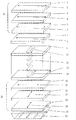
図1に示す液晶表示装置は、液晶セル(9〜13)、液晶セルを挟持して配置された上側偏光板21(1〜6)と下側偏光板22(14〜19)、及び下側偏光板22のさらに外側に、光源となるランプ20aを含むバックライトユニット20を有する。液晶セル(9〜13)は、液晶セル上側基板9と液晶セル下側基板12と、これらに挟持される液晶層11とを含む。下側基板12は、その対向面に、電極層(図1中、不図示)を有し、該電極層は、基板12の表面に対して平行な電界を液晶層に供与可能に構成されている。電極層は通常透明なインヂウムチンオキサイド(ITO)からなる。基板12の電極層上及び基板9の対向面には、液晶性分子11の配向を制御する配向層(図1中不図示)が形成され、駆動電圧非印加時においては、その表面に施されたラビング処理の方向10及び13によって、液晶性分子11の配向方向が制御されている。
Hereinafter, embodiments of the present invention using RGB color filters will be described with reference to the drawings.
The liquid crystal display device shown in FIG. 1 includes a liquid crystal cell (9 to 13), an upper polarizing plate 21 (1 to 6) and a lower polarizing plate 22 (14 to 19) disposed between the liquid crystal cells, and a lower side. A
電極の形状、構成等については特に制限されず、液晶セルの基板に対して平行な電界を形成可能である限り、いずれであってもよい。一般的に、IPSモード及びFFSモードの液晶表示装置に用いられている電極構成を利用することができる。例えば、層を異にして配置された画素電極と対向電極によって構成してもよいし、層を異にして配置された少なくとも一方が透明な一対の電極と、電圧が印加されない電極とで構成してもよい。 The shape, configuration, etc. of the electrode are not particularly limited, and any may be used as long as an electric field parallel to the substrate of the liquid crystal cell can be formed. In general, electrode configurations used in IPS mode and FFS mode liquid crystal display devices can be used. For example, a pixel electrode and a counter electrode arranged in different layers may be used, or at least one of the electrodes arranged in different layers may be composed of a pair of transparent electrodes and an electrode to which no voltage is applied. May be.
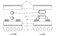
図2に、IPSモードの液晶標示装置の一例についての、OFF状態及びON状態を模式的に示す。なお、図2は、液晶表示装置の一画素の一部分を示しているものであり、各部材の相対的な大きさ等は、実際のものと必ずしも一致していない。後述する図3においても同様である。また、図2中、図1中の部材に対応する部材には同一の符号を付した。後述する図3においても同様である。
図2中、基板12の対向面に形成された複数の線状電極層24は、電圧印加時に基板12の平面に平行な電界成分を含む電界23を形成する。電圧無印加時又は低電圧印加時(OFF状態)には、液晶性分子11は、基板9及び12の対向面のラビング軸(図1において10及び13)によって、線状電極層24の長手方向に対して若干の角度を持つように配向制御されている。なお、この場合の液晶の誘電異方性は正を想定している。線状電極層24に電圧を印加した状態(ON状態)では、基板9及び12に平行な成分を含む電界23が形成され、液晶性分子11はその長軸を電界方向と一致させて配向する。なお、基板12の表面に対する電界方向23のなす角は、好ましくは20度以下で、より好ましくは10度以下で、すなわち、実質的に平行であることが望ましい。以下、本発明では20度以下のものを総称して平行電界と表現する。また、線状電極層24を上下基板に分けて形成しても、一方の基板にのみ形成してもその効果は変わらない。
FIG. 2 schematically shows an OFF state and an ON state of an example of an IPS mode liquid crystal display device. Note that FIG. 2 shows a part of one pixel of the liquid crystal display device, and the relative sizes and the like of the respective members do not necessarily coincide with the actual ones. The same applies to FIG. 3 described later. In FIG. 2, members corresponding to the members in FIG. The same applies to FIG. 3 described later.
In FIG. 2, the plurality of linear electrode layers 24 formed on the opposing surface of the
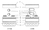
図3に、FFSモードの液晶標示装置の一例についての、OFF状態及びON状態を模式的に示す。なお、図2中と同一の部材には同一の番号を付し、詳細な説明は省略する。
図3では、電極は、上層の電極層24と下層の電極層26との2層構造となっていて、絶縁層25を介して層を異にして配置されている。電極層26は、パターニングされていない電極層であっても、線状などにパターニングされた電極層であってもよい。上層の電極層24は線状であるのが好ましいが、下層電極層26からの電界が通過できる形状であれば、網目状、スパイラル状及び点状などいずれでもよい。電位が中立なフローティング電極をさらに追加してもよい。また絶縁層25はSiOや窒化膜などの無機材料からなる層であっても、アクリルやエポキシ系等の有機材料からなる層であってもよい。上層の電極層24と下層の電極層26とに電圧を印加することによって、基板8に対して平行な成分を含む電界23’が形成される。OFF状態においては、IPSモードと同様、液晶性分子11は、基板9及び12の対向面のラビング軸(図1において10及び13)にその長軸を一致させて配向する。それに対し、ON状態では、基板9及び2に平行な成分を含む電界23’が形成され、液晶性分子11はその長軸を電界方向と一致させて配向する。
FIG. 3 schematically shows an OFF state and an ON state of an example of an FFS mode liquid crystal display device. In addition, the same number is attached | subjected to the member same as FIG. 2, and detailed description is abbreviate | omitted.
In FIG. 3, the electrode has a two-layer structure of an
なお、図1には詳細な構造は示さないが、液晶セルの上側基板9又は下側基板12の対向面には、RGBカラーフィルタが配置され、液晶セルはR層、G層及びB層が配置された3つの絵素領域を含んでいる。本実施態様では、これらの3つの着色層のうち、少なくとも2つの着色層、例えば、G層とR層、又はG層とB層、の厚さ方向のRthが互いに異なっている。3つの着色層のRthがそれぞれ互いに異なっているのがより好ましい。RGBカラーフィルタでは、絵素領域の最大透過率をとる主波長は、小さい順に、青色光波長λB、緑色光波長λG及び赤色光波長λRになる。R、G及びB層におけるカラーフィルタの厚み方向のレターデーションをRth(λB)、Rth(λG)及びRth(λR)とすると、本実施形態では、RGBカラーフィルタのRth(λB)は、下記関係式(I)を満足する。より色再現性を改善するためには、Rth(λG)及びRth(λR)についても調整するのが好ましいが、その好ましい範囲は、偏光板用液晶セル側保護フィルム5及び14の光学特性に依存する。
例えば、図1中、偏光板用液晶セル側保護フィルム5及び/又は14(好ましくは5及び14)として、下記式(2)−1〜(2)−4を満たすポリマーフィルムを用いた例では、さらに、RGBカラーフィルタのRth(λG)及びRth(λR)の少なくとも一方が、下記式(II)及び(III)のそれぞれを満足しているのが好ましく、双方が、下記式(II)及び(III)を満足しているのがより好ましい。
(I): Rth(λB)≦ 5nm
(II): −35nm ≦Rth(λG)≦ 25nm
(III): −45nm ≦Rth(λR)≦ 0nm
(2)−1 0nm≦ Re(630)≦ 10nm
(2)−2 |Rth(630)|≦ 80nm
(2)−3 |Re(400)−Re(700)|≦ 20nm
(3)−4 |Rth(400)−Rth(700)|≦ 45nm 。
Although a detailed structure is not shown in FIG. 1, RGB color filters are arranged on the opposing surface of the
For example, in FIG. 1, in the example using the polymer film which satisfy | fills following formula (2) -1-(2) -4 as the liquid crystal cell side
(I): Rth (λ B ) ≦ 5 nm
(II): −35 nm ≦ Rth (λ G ) ≦ 25 nm
(III): −45 nm ≦ Rth (λ R ) ≦ 0 nm
(2) -10 0 nm ≦ Re (630) ≦ 10 nm
(2) -2 | Rth (630) | ≦ 80 nm
(2) -3 | Re (400) -Re (700) | ≦ 20 nm
(3) -4 | Rth (400) -Rth (700) | ≦ 45 nm.
前記式(2)−1〜(2)−4を満たすポリマーフィルムとしては、面内レターデーションReがほぼ0であり、且つ厚さ方向のレターデーションRthが40nm程度のセルロースアシレートフィルムが挙げられる。 Examples of the polymer film satisfying the formulas (2) -1 to (2) -4 include a cellulose acylate film having an in-plane retardation Re of almost 0 and a thickness direction retardation Rth of about 40 nm. .
また、図1中の偏光板用液晶セル側保護フィルム5及び/又は14(好ましくは5及び14)として、下記式(3)−1〜(3)−4の全てを満足するフィルム(好ましくはセルロースアシレートフィルム)を用いた例では、Rth(λB)が、前記関係式(I)を満足するとともに、さらに、RGBカラーフィルタのRth(λG)及びRth(λR)の少なくとも一方が、下記式(II)’及び(III)’のそれぞれを満足しているのが好ましく、双方が、下記式(II)’及び(III)’を満足しているのがより好ましい。
(II)’: −20nm≦ Rth(λG)≦ 10nm
(III)’: −15nm≦ Rth(λR)≦ 20nm
(3)−1: 0nm≦ Re(630)≦ 10nm
(3)−2: |Rth(630)|≦ 25nm
(3)−3: |Re(400)−Re(700)|≦ 10nm
(3)−4: |Rth(400)−Rth(700)|≦ 35nm
Moreover, as the liquid crystal cell side
(II) ′: −20 nm ≦ Rth (λ G ) ≦ 10 nm
(III) ′: −15 nm ≦ Rth (λ R ) ≦ 20 nm
(3) -1: 0 nm ≦ Re (630) ≦ 10 nm
(3) -2: | Rth (630) | ≦ 25 nm
(3) -3: | Re (400) -Re (700) | ≦ 10 nm
(3) -4: | Rth (400) -Rth (700) | ≦ 35 nm
かかる関係式を満足するため、例えば、R層の厚み(dr)、G層の厚み(dg)、及びB層の厚み(db)が互いに異なるカラーフィルタを用いてもよい。 In order to satisfy this relational expression, for example, color filters having different R layer thickness (d r ), G layer thickness (d g ), and B layer thickness (d b ) may be used.
再び図1において、液晶セルは、上側偏光板21と下側偏光板22との間に配置され、上側偏光板21及び下側偏光板22は互いにその吸収軸4及び17を直交にして配置される。上側偏光板21を視認側偏光板とした場合、上側偏光板21の吸収軸4は、電圧無印加時(OFF状態)における、液晶セル内の液晶性分子11の異常光屈折率方向と直交するように積層するのが好ましい。上側偏光板21は、偏光フィルム3と、その表面に配置された保護フィルム1及び5とを有し、下側偏光板22は、偏光フィルム16と、その表面に配置された保護フィルム14及び18とを有する。
In FIG. 1 again, the liquid crystal cell is disposed between the upper
なお、偏光フィルム3及び16の表面に配置される保護フィルム1、5及び14、18は、一般的には延伸フィルムからなり、MD(Mechanical direction)方向、もしくはTD(Tenter direction)と一致した遅相軸を有する。一つの偏光フィルム3(又は6)の表面に配置される2つの保護フィルム1,5(又は14、18)のMD方向は、図1中の上側偏光板21の様に、互いに平行(図1中の2と6)であってもよいし、図1中の下側偏光板22の様に、互いに直交(図1中の15と19)していてもよい。
The
図1において、下側偏光板22の外側に配置されたバックライトユニット20から光が入射する場合を考える。電極(図1中不図示)に駆動電圧を印加しない非駆動状態(OFF状態)では、液晶層中の液晶性分子11は、基板9及び12の面に対して概略平行に、且つその長軸をラビング軸10及び13に略平行にして配向している。この状態では、偏光フィルム16によって所定の偏光状態となった光は、液晶性分子11の複屈折効果を受けず、その結果、偏光フィルム3の吸収軸4によってブロックされる。この時、黒表示となる。これに対して、電極(図1中不図示)に駆動電圧を印加した駆動状態(ON状態)では、基板に対して平行な成分を含む電界が形成され、液晶性分子11はその長軸を電界の向きに一致させて配向する。その結果、偏光フィルム18によって所定の偏光状態となった光は、液晶性分子11の複屈折効果によって偏光状態が変化し、その結果、偏光フィルム3を通過する。この時白表示となる。本発明では、カラーフィルタの厚み方向のレターデーションRthを各絵素領域ごとに異ならせているので、広い視野角で良好な色再現性が得られ、且つ黒表示時の着色、いわゆるカラーシフトが軽減されている。
In FIG. 1, consider a case where light is incident from a
図2のIPSモードの液晶表示装置では、液晶層の配向制御方向(図1中、ラビング軸10及び13)を、表示装置の上下方向、12時−6時方向、として配置するのが好ましく、上側偏光板と下側偏光板の吸収軸4及び17も、12時−6時方向に配置して、直交させるのが好ましい。さらに、偏光フィルム3及び16と、液晶層との間に配置される保護フィルム5及び14の遅相軸6及び15も、12時−6時で配置して、より近い位置に配置された液晶セル用基板のラビング軸と平行にして配置するのが好ましい。かかる配置は、黒表示時の漏れ光の低減や視角方向での着色の解消に有効である。
In the IPS mode liquid crystal display device of FIG. 2, the alignment control direction of the liquid crystal layer (rubbing
さらに、図1に示す様に、上側偏光板21の液晶セル側保護フィルム5と液晶層11との間に光学異方性層7を配置してもよい。光学異方性層7のレターデーションの値は、液晶層11のΔn・dの値の2倍以下に設定するのが好ましい。なお、図1では、光学異方性層7を、上側偏光板21の保護フィルム5と液晶層11との間に配置した構成を示したが、下側偏光板22の保護フィルム14と液晶層11との間に配置してもよいし、また、双方に配置してもよい。また、上側偏光フィルム3の保護フィルム5のレターデーションは、下側偏光フィルム16の保護フィルム14のレターデーションより、Rthが20nm以上大きいと、黒表示時の漏れ光の低減や視角方向での着色の解消に有効である。
Further, as shown in FIG. 1, the optically
図3に示すFFS方式液晶表示装置では、液晶層の配向制御方向(図1中、ラビング軸10及び13)を、表示装置の左右方向、3時−9時方向として配置するのが好ましく、上側偏光板と下側偏光板の吸収軸4及び17も、3時−9時方向に配置して、直交させるのが好ましい。さらに、偏光フィルム3及び16と、液晶層との間に配置される保護フィルム5及び14の遅相軸6及び11も、3時−9時で配置して、より近い位置に配置された液晶セル用基板のラビング軸と平行にして配置するのが好ましい。かかる配置は、黒表示時の漏れ光の低減や視角方向での着色の解消に有効である。さらに、図1に示す様に、上側偏光板21の液晶セル側保護フィルム5と液晶層11との間に光学異方性層7を配置してもよい。光学異方性層7のレターデーションの値は、液晶層11のΔn・dの値の2倍以下に設定するのが好ましい。なお、図1では、光学異方性層7を、上側偏光板21の保護フィルム5と液晶層11との間に配置した構成を示したが、下側偏光板22の保護フィルム14と液晶層11との間に配置してもよいし、また、双方に配置してもよい。
In the FFS mode liquid crystal display device shown in FIG. 3, the alignment control direction (rubbing
電極の形状及び配置については図2及び3に示す構成に限定されず、従来、IPSモード及びFFSモードに利用されているいずれの形状の電極及びその構成を利用することができる。例えば、より広視野角を得るために、線状電極(「くし歯電極」という場合がある)をジグザグの形状に配置してもよい。ただしこの場合は、電極の屈曲部で液晶層中の液晶性分子の配向が乱れ、表示装置のコントラストが低下する場合がある。このコントラストの低下を軽減するのに、偏光フィルム(図1中3及び16)のセルロースアシレートフィルム等からなる保護フィルム(図1中5及び14)の遅相軸(図1中、6及び15)を、液晶層11の平均配向制御方向(図1中10及び13)と10°以内で交差させるのが有効である。この様に配置すると、この配向乱れによる液晶層の位相差ムラを補償することができ、表示の均一性を向上させることができる。さらにラビング処理による液晶分子の配向乱れによる黒表示時の輝度ムラも、保護フィルムを、その遅相軸をラビング軸に対して交差させて配置することで、レターデーションムラを自己補償して、輝度ムラを軽減できる。
これら液晶分子の配向乱れの平均の方向は元々の配向制御方向から概略5〜15°程度ずれている。保護フィルムの遅相軸をその平均配向軸に交差させて,レターデーションを補償することで表示ムラが軽減できる。なお、上記した様に、保護フィルムをその遅相軸を交差させて配置する場合は、保護フィルムのRe値が大きいと、ムラは軽減できても、黒輝度絶対値が上昇し,コントラスト低下が発生してしまう場合があるので、例えば、特開2005−138375号公報に記載のセルロースアシレートフィルム等の、Reが小さい、ほぼ0のフィルムを用いるのが好ましい。
さらに上記した通り、光学異方性層を配置し、その遅相軸や配向制御方向、平均の配向方向を、液晶層の平均配向制御方向と10°以内で交差させることでも同様にムラを低減することができる。
The shape and arrangement of the electrodes are not limited to the configurations shown in FIGS. 2 and 3, and any shape electrodes and configurations conventionally used in the IPS mode and the FFS mode can be used. For example, in order to obtain a wider viewing angle, linear electrodes (sometimes referred to as “comb electrodes”) may be arranged in a zigzag shape. However, in this case, the orientation of the liquid crystal molecules in the liquid crystal layer is disturbed at the bent portion of the electrode, and the contrast of the display device may be lowered. In order to reduce this decrease in contrast, the slow axis (6 and 15 in FIG. 1) of the protective film (5 and 14 in FIG. 1) made of a cellulose acylate film or the like of the polarizing film (3 and 16 in FIG. 1) or the like. ) With the average orientation control direction (10 and 13 in FIG. 1) of the
The average direction of the alignment disorder of these liquid crystal molecules deviates from the original alignment control direction by about 5 to 15 °. Display unevenness can be reduced by compensating the retardation by crossing the slow axis of the protective film with the average orientation axis. As described above, when the protective film is arranged with its slow axis intersected, if the Re value of the protective film is large, even if the unevenness can be reduced, the black luminance absolute value increases and the contrast decreases. Since it may occur, for example, it is preferable to use a film having a small Re and almost zero, such as a cellulose acylate film described in JP-A-2005-138375.
Furthermore, as described above, an optically anisotropic layer is arranged, and unevenness can be similarly reduced by intersecting the slow axis, orientation control direction, and average orientation direction with the average orientation control direction of the liquid crystal layer within 10 °. can do.
また、FFSモードは、視野角がIPSモードより狭くなる傾向があり、また、電極端で高電界が印加されるため液晶配向乱れが大きいという特徴がる。これらのことから、セルロース氏レートフィルム等からなる保護フィルム(図1中5及び14)の遅相軸(図1中6及び15)を液晶層11の平均配向制御方向(図1中10及び13)と10°以内で交差させることによるムラ低減の効果はより大きくなる。
なお、IPSモード及びFFSモードのいずれの態様の液晶表示装置においても、視認側及びバックライト側の偏光板の双方又はいずれか一方について、保護フィルムの遅相軸と偏光フィルムとの吸収軸とが前記範囲でずれているのが好ましく、いずれか一方のみについて、保護フィルムの遅相軸と偏光フィルムとの吸収軸とが前記範囲でずれているのがより好ましい。
In addition, the FFS mode has a tendency that the viewing angle tends to be narrower than that of the IPS mode, and the liquid crystal alignment disorder is large because a high electric field is applied at the electrode end. From these facts, the slow axis (6 and 15 in FIG. 1) of the protective film (5 and 14 in FIG. 1) made of a cellulose film or the like is the average orientation control direction of the liquid crystal layer 11 (10 and 13 in FIG. 1). ) And within 10 °, the effect of reducing unevenness is further increased.
In both the IPS mode and the FFS mode liquid crystal display device, the slow axis of the protective film and the absorption axis of the polarizing film are provided for both or one of the viewing-side and backlight-side polarizing plates. It is preferable that it is shifted within the above range, and it is more preferable that the slow axis of the protective film and the absorption axis of the polarizing film are shifted within the above range.
以下、本発明の液晶表示装置に使用可能な各部材等について詳細に説明する。
[液晶材料]
本発明の液晶表示装置に用いられる液晶層を構成する液晶材料については特に制限されない。図1に示す構成の液晶表示装置には、例えば、液晶材料として、誘電率異方性△εが正のネマチック液晶を用いてもよい。液晶層の厚み(ギャップ)は、2.8μm超4.5μm未満程度とするのが好ましい。液晶層のレターデーション(Δn・d)を0.25μm超0.32μm未満とすると、可視光の範囲内で波長依存性が殆どない透過率特性がより容易に得られる。液晶性分子がラビング方向から電界方向に45度回転したとき最大透過率を得ることができる。なお、液晶層の厚み(ギャップ)はポリマビーズで制御している。もちろんガラスビーズヤファイバー、樹脂製の柱状スペーサでも同様のギャップを得ることができる。また液晶材料LCは、ネマチック液晶であれば、特に限定したものではない。誘電率異方性△εは、その値が大きいほうが、駆動電圧が低減でき、屈折率異方性△nは小さいほうが液晶層の厚み(ギャップ)を厚くでき、液晶の封入時間が短縮され、かつギャップばらつきを少なくすることができる。
Hereafter, each member etc. which can be used for the liquid crystal display device of this invention are demonstrated in detail.
[Liquid crystal materials]
The liquid crystal material constituting the liquid crystal layer used in the liquid crystal display device of the present invention is not particularly limited. In the liquid crystal display device having the configuration shown in FIG. 1, for example, nematic liquid crystal having a positive dielectric anisotropy Δε may be used as the liquid crystal material. The thickness (gap) of the liquid crystal layer is preferably more than 2.8 μm and less than 4.5 μm. When the retardation (Δn · d) of the liquid crystal layer is more than 0.25 μm and less than 0.32 μm, a transmittance characteristic having almost no wavelength dependency within the visible light range can be obtained more easily. Maximum transmittance can be obtained when the liquid crystal molecules are rotated 45 degrees from the rubbing direction to the electric field direction. The thickness (gap) of the liquid crystal layer is controlled by polymer beads. Of course, the same gap can be obtained with glass bead fiber or resin columnar spacers. The liquid crystal material LC is not particularly limited as long as it is a nematic liquid crystal. As the value of the dielectric anisotropy Δε is larger, the driving voltage can be reduced, and as the refractive index anisotropy Δn is smaller, the thickness (gap) of the liquid crystal layer can be increased, and the liquid crystal sealing time is shortened. In addition, gap variation can be reduced.
[液晶セル]
本発明の液晶表示装置に用いる液晶セルは、少なくとも一方が電極を有する対向配置された一対の基板と、該基板間に配置され、配向制御された液晶層とを有する。液晶セル用基板の内側の対向面の双方に、液晶分子を配向させる配向膜を形成するのが好ましい。また、いずれか一方の対向面に、カラーフィルタを形成するのが好ましい。さらに、液晶セルの内側に偏光フィルムを配置してもよいし、また液晶層のレターデーションの光学補償に寄与する光学異方性層を配置してもよい。また、2枚の基板間の距離(セルギャップ)を保持するための柱状あるいは球状のスペーサを配置するのが一般的である。その他、反射板、集光レンズ、輝度向上フィルム、発光層、蛍光層、燐光層、反射防止膜、防汚膜、ハードコート膜等をセル内に配置してもよい。
[Liquid Crystal Cell]
The liquid crystal cell used in the liquid crystal display device of the present invention has a pair of substrates, at least one of which has electrodes, and a liquid crystal layer that is disposed between the substrates and the alignment of which is controlled. It is preferable to form an alignment film for aligning liquid crystal molecules on both inner surfaces of the liquid crystal cell substrate. Moreover, it is preferable to form a color filter on any one of the opposing surfaces. Furthermore, a polarizing film may be disposed inside the liquid crystal cell, or an optically anisotropic layer that contributes to optical compensation of retardation of the liquid crystal layer may be disposed. In general, a columnar or spherical spacer is disposed to maintain a distance (cell gap) between two substrates. In addition, a reflector, a condenser lens, a brightness enhancement film, a light emitting layer, a fluorescent layer, a phosphorescent layer, an antireflection film, an antifouling film, a hard coat film, and the like may be disposed in the cell.
液晶セル用の基板は透明ガラス基板を用いるのが一般的であるが、より硬く高温に耐えるシリコンガラス基板を用いてもよい。また耐熱性の優れたプラスチック基板、高分子材料による基板を用いてもよい。変形可能な材料により基板を使用してフレキシブルやリーラブルディスプレイも有効である。さらに反射型表示装置では基板の一方が透明であればよく、他方にステンレス等の金属基板を用いることも可能である。 A transparent glass substrate is generally used as the substrate for the liquid crystal cell, but a silicon glass substrate that is harder and can withstand high temperatures may be used. Further, a plastic substrate having excellent heat resistance or a substrate made of a polymer material may be used. A flexible or reelable display using a substrate made of a deformable material is also effective. Further, in the reflective display device, one of the substrates may be transparent, and a metal substrate such as stainless steel may be used for the other.
本発明では、液晶表示装置は、3つの絵素領域を含む。例えば、カラーフィルタを有する、カラー表示を行う液晶表示装置では、光の3原色、赤、緑、青のサブピクセル(絵素領域)が1組となり、通常1画素を形成する。また3色以上のサブピクセルで1画素を形成する場合もある。本発明の一態様として、一画素を構成している各色のサブピクセルにおいて、それぞれセルギャップが異なるマルチギャップの態様が挙げられる。
また、1画素を複数の領域に分割するマルチドメインと呼ばれる構造にして、色バランスの調整や視野角特性の平均化を行ってもよい。
In the present invention, the liquid crystal display device includes three picture element regions. For example, in a liquid crystal display device that has a color filter and performs color display, the sub-pixels (picture element regions) of the three primary colors of light, red, green, and blue form one set and usually form one pixel. In some cases, one pixel is formed by sub-pixels of three or more colors. As one aspect of the present invention, there is a multi-gap aspect in which the cell gap is different in each color sub-pixel constituting one pixel.
Further, a structure called a multi-domain in which one pixel is divided into a plurality of regions may be used to adjust the color balance and average the viewing angle characteristics.
[カラーフィルタ]
本発明では、液晶セルの一対の基板の一方の対向面に、カラーフィルタを配置するのが好ましい。カラーフィルタについては特に制限されないが、例えば、赤色(R)、緑色(G)及び青色(B)の各層を含むカラーフィルタを配置するのが好ましい。
前述のように本発明の液晶表示装置では、前記液晶セルが、3つの絵素領域を含み、これらのうち少なくとも2つの絵素領域のそれぞれに配置されたカラーフィルタのRthが互いに異なることが好ましい。3つの絵素領域のそれぞれに配置されたカラーフィルタのRthが互いに異なっているのがより好ましい。この構成を達成する好ましい手段の一つは、前記3つの絵素領域のそれぞれに配置されたカラーフィルタの厚さのうち、少なくとも2つの絵素領域に配置されたカラーフィルタの厚さを異なる厚さにすることが挙げられる。
これによって前記3つの絵素領域のそれぞれに配置されたカラーフィルタのRthのうち、少なくとも2つの絵素領域のそれぞれに配置されたカラーフィルタのRthを、互いに異ならせることができ、本発明の課題をより効果的に達成することができる。
[Color filter]
In the present invention, it is preferable to dispose a color filter on one opposing surface of the pair of substrates of the liquid crystal cell. Although it does not restrict | limit especially about a color filter, For example, it is preferable to arrange | position the color filter containing each layer of red (R), green (G), and blue (B).
As described above, in the liquid crystal display device of the present invention, it is preferable that the liquid crystal cell includes three picture element regions, and Rth of color filters arranged in at least two of these pixel regions are different from each other. . More preferably, the Rths of the color filters arranged in each of the three picture element regions are different from each other. One of the preferable means for achieving this configuration is that the thickness of the color filter arranged in at least two pixel regions is different from the thickness of the color filter arranged in each of the three pixel regions. There is a thing to do.
Accordingly, among the Rths of the color filters arranged in each of the three picture element regions, the Rths of the color filters arranged in each of the at least two picture element regions can be made different from each other. Can be achieved more effectively.
カラーフィルタは、例えば、以下の方法で作製することができる。先ず、透明基板上に赤色、緑色、青色等の、目的に合せた着色画素を形成する。透明基板上に赤色、緑色、青色等の着色画素を形成する方法としては、前述した染色法、印刷法、又は着色感光性樹脂液をスピンコーター等で塗布後、フォトリソ工程でパターニングする着色レジスト法、さらにはラミネート法等が適宜利用できる。例えば、塗布工程を含む形成方法では、塗布量を調整することで、厚さの異なるRGB層を有するカラーフィルタを形成できる。また、ラミネート法を利用する場合は、厚さが異なる転写材料を用いることで、厚さの異なるRGB層からなるカラーフィルタを形成できる。 The color filter can be produced, for example, by the following method. First, colored pixels, such as red, green, and blue, that match the purpose are formed on a transparent substrate. As a method of forming colored pixels such as red, green, and blue on a transparent substrate, the above-described staining method, printing method, or coloring resist method in which a colored photosensitive resin liquid is applied with a spin coater or the like and then patterned in a photolithography process. Furthermore, a laminating method or the like can be used as appropriate. For example, in a formation method including a coating process, a color filter having RGB layers having different thicknesses can be formed by adjusting the coating amount. In the case of using a laminate method, a color filter composed of RGB layers having different thicknesses can be formed by using transfer materials having different thicknesses.
黒色感光性樹脂を用いてブラックマトリクスを形成する場合は、上記着色画素を形成した後にするのが好ましい。最初にブラックマトリクスを形成すると、光学濃度の高い黒色感光性樹脂では、樹脂表面しか硬化しないため、次いで行われる現像処理、特に着色画素を形成するため繰り返し行う現像処理により未硬化の樹脂が溶け出し(サイドエッチと称する)、極端な場合には形成されたマトリクスが剥がれてしまうこともあるからである。
これに対し、ブラックマトリクスを最後に形成すれば、ブラックマトリクスの周囲は着色画素で囲まれていて、断面からは現像液が浸透しにくいため、サイドエッチが起こりにくく、光学濃度の高いブラックマトリクスを形成できるという大きな利点がある。
更に、着色画素形成用の着色層の形成をラミネート法で行う場合は、先にブラックマトリクスを形成すると、着色画素が形成されるべき場所がブラックマトリクスでほぼ格子状に閉じられているため、ラミネート時に気泡を巻き込み易いという問題があるが、後にブラックマトリックスを形成すれば、かかる問題は生じないので好ましい。
When forming a black matrix using a black photosensitive resin, it is preferable to form it after forming the colored pixels. When a black matrix is first formed, only the resin surface is cured with a black photosensitive resin having a high optical density, so that the uncured resin is melted by the subsequent development process, particularly the repeated development process for forming colored pixels. This is because the formed matrix may be peeled off in an extreme case (referred to as side etching).
In contrast, if the black matrix is formed last, the periphery of the black matrix is surrounded by colored pixels, and the developer is difficult to penetrate from the cross section. There is a great advantage that it can be formed.
Furthermore, when the colored layer for forming the colored pixels is formed by the laminating method, if the black matrix is formed first, the place where the colored pixels are to be formed is closed in a substantially lattice pattern by the black matrix. Although there is a problem that air bubbles are sometimes easily involved, it is preferable to form a black matrix later because this problem does not occur.
黒色感光性樹脂の感光波長域に対する着色画素の光透過率が2%を超える場合は、予め着色画素の中に光吸収剤等を加え、その透過率を2%以下にすることが好ましい。この際使用する光吸収剤としては公知の種々の化合物を用いることができる。例えば、ベンゾフェノン誘導体(ミヒラーズケトン等)、メロシアニン系化合物、金属酸化物、ベンゾトリアゾール系化合物、クマリン系化合物等を挙げることができる。その中でも、光吸収性が良好で、かつ200℃以上の熱処理の後でも25%以上の光吸収性能を保持するものが好ましく、具体的には酸化チタン、酸化亜鉛、ベンゾトリアゾール系化合物、クマリン系化合物が挙げられる。これらの中では、クマリン系化合物が耐熱性、光吸収性の両観点から特に好ましい。尚、上述の200℃以上の熱処理は、各画素を形成後、一層硬化させるために行われるものである。 When the light transmittance of the colored pixel with respect to the photosensitive wavelength region of the black photosensitive resin exceeds 2%, it is preferable to add a light absorber or the like into the colored pixel in advance so that the transmittance is 2% or less. Various known compounds can be used as the light absorber used in this case. Examples include benzophenone derivatives (such as Michler's ketone), merocyanine compounds, metal oxides, benzotriazole compounds, and coumarin compounds. Among them, those that have good light absorption and retain 25% or more of light absorption performance even after heat treatment at 200 ° C. or higher are preferable. Specifically, titanium oxide, zinc oxide, benzotriazole compounds, coumarin compounds Compounds. Among these, coumarin compounds are particularly preferable from the viewpoints of both heat resistance and light absorption. The above-described heat treatment at 200 ° C. or higher is performed in order to further cure after forming each pixel.
次に、画素パターンを覆って透明基板全面に黒色感光性樹脂層を設けるが、これも黒色感光性樹脂液をスピンコーターやロールコーターで塗布する方法、また、予め黒色感光性樹脂液を仮支持体上に塗布することにより画像形成材料を作成し、画素パターン上にこの黒色感光性樹脂層を転写する方法等が利用できる。 Next, a black photosensitive resin layer is provided on the entire surface of the transparent substrate so as to cover the pixel pattern. This is also a method of applying a black photosensitive resin liquid with a spin coater or a roll coater, or temporarily supporting the black photosensitive resin liquid in advance. An image forming material can be prepared by coating on the body, and the black photosensitive resin layer can be transferred onto the pixel pattern.
次に、フォトマスクを介して黒色感光性樹脂層側から露光し、着色画素が存在しない遮光部(ブラックマトリックス)の黒色感光性樹脂層を硬化させる。着色画素は、露光機のアライメント誤差や基板の熱膨張の影響を受けて多少の位置ずれがあり、画素自体の太りや細りがあって、設計寸法通りの間隔や大きさで配置されてはいないのが普通である。特に大サイズの基板ではこの傾向が強くなる。したがって、設計画素間隔通りのフォトマスクで露光した場合、ブラックマトリックスが画素と重なる部分や、逆に画素との間に隙間ができる部分が発生する。重なった部分は突起になり、隙間ができた部分は光漏れになるので何れも好ましくない。 Next, it exposes from the black photosensitive resin layer side through a photomask, and the black photosensitive resin layer of the light-shielding part (black matrix) in which a coloring pixel does not exist is hardened. The colored pixels are slightly misaligned due to the alignment error of the exposure tool and the thermal expansion of the substrate, the pixels themselves are thick and thin, and are not arranged at the designed dimensions. Is normal. This tendency is particularly strong for large-sized substrates. Therefore, when exposure is performed with a photomask according to the design pixel interval, a portion where the black matrix overlaps with the pixel or a portion where a gap is formed between the pixel is generated. Since the overlapped portion becomes a protrusion, and the portion where the gap is formed becomes light leakage, both are not preferable.
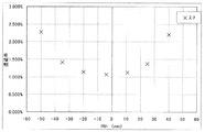
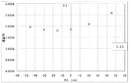
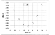
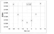
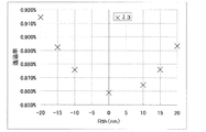
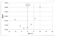
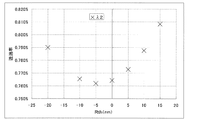
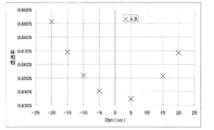
本発明では、前記カラーフィルタは最大透過率をとる3つの主波長(λ1<λ2<λ3)のうち、波長λ1におけるカラーフィルタの厚さ方向のレターデーションRth(λ1)が、下記式(I)を満たす。
式(I) : Rth(λ1)≦ 5nm 。
Rth(λ1)が5nm以下であれば、負の値であってもよく、その下限値については特に制限されないが、既存の材料を用いて製造可能な範囲を考慮すると、下限値は−65nm程度である。Rth(λ1)は、−30nm〜−50nmであるのが好ましい。
偏光板用液晶セル側保護フィルムとして、前記式(2)−1〜(2)−4の全てを満足するポリマーフィルム(例えば、面内レターデーションReがほぼ0であり、且つ厚さ方向のレターデーションRthが40nm程度のセルロースアシレートフィルム)を備えた液晶表示装置において、色再現性をより改善するためには、前記カラーフィルタは、Rth(λ2)が、−35〜25nmであるのが好ましく、−27nm〜22nmであるのがより好ましい。同観点から、Rth(λ3)は、−45〜0nmであるのが好ましく、−38nm〜−1nmであるのがより好ましい。
また、偏光板用液晶セル側保護フィルムとして、前記式(3)−1〜(3)−4の光学特性を満足するポリマーフィルムを備えた液晶表示装置において、色再現性をより改善するためには、前記カラーフィルタは、Rth(λ2)が、−20〜10nmであるのが好ましく、−15nm〜5nmであるのがより好ましい。同観点から、Rth(λ3)は、−15〜20nmであるのが好ましく、−10nm〜15nmであるのがより好ましい。
In the present invention, the color filter has a retardation Rth (λ 1 ) in the thickness direction of the color filter at the wavelength λ 1 among the three main wavelengths (λ 1 <λ 2 <λ 3 ) having the maximum transmittance. The following formula (I) is satisfied.
Formula (I): Rth (λ 1 ) ≦ 5 nm.
If Rth (λ 1 ) is 5 nm or less, it may be a negative value, and the lower limit is not particularly limited, but considering the range that can be produced using existing materials, the lower limit is −65 nm. Degree. Rth (λ 1 ) is preferably −30 nm to −50 nm.
As a protective film on the liquid crystal cell side for a polarizing plate, a polymer film satisfying all of the above formulas (2) -1 to (2) -4 (for example, the in-plane retardation Re is almost zero and the thickness direction letter is In order to further improve color reproducibility in a liquid crystal display device including a cellulose acylate film having a foundation Rth of about 40 nm, Rth (λ 2 ) of the color filter is −35 to 25 nm. Preferably, it is -27 nm-22 nm. From the same viewpoint, Rth (λ 3 ) is preferably −45 to 0 nm, and more preferably −38 nm to −1 nm.
Moreover, in order to improve color reproducibility more in the liquid crystal display device provided with the polymer film which satisfies the optical characteristic of said Formula (3) -1-(3) -4 as a liquid crystal cell side protective film for polarizing plates. In the color filter, Rth (λ 2 ) is preferably −20 to 10 nm, and more preferably −15 nm to 5 nm. From the same viewpoint, Rth (λ 3 ) is preferably −15 to 20 nm, and more preferably −10 nm to 15 nm.
カラーフィルタのレターデーションは、例えば、カラーフィルタを転写材料を用いて作製する場合は、転写材料の構成層である感光層や着色層にレターデーション上昇剤や低下剤を添加することにより調整してもよい。
レターデーション上昇剤の代表例としては、下記一般式(X)で表される化合物及びこれに類似する化合物が挙げられる。
The retardation of the color filter is adjusted, for example, by adding a retardation increasing agent or reducing agent to the photosensitive layer or the colored layer, which is a constituent layer of the transfer material, when the color filter is prepared using a transfer material. Also good.
Representative examples of the retardation increasing agent include compounds represented by the following general formula (X) and compounds similar thereto.
レターデーション低下剤の例は、下記一般式(XI)で表される化合物がある。 Examples of the retardation reducing agent include compounds represented by the following general formula (XI).
上記一般式(XI)中、R11はアルキル基又はアリール基を表し、R12及びR13は、それぞれ独立に、水素原子、アルキル基又はアリール基を表す。また、R11、R12及びR13の炭素原子数の総和が10以上であることが特に好ましい。R11、R12及びR13は置換基を有していてもよく、置換基としてはフッ素原子、アルキル基、アリール基、アルコキシ基、スルホン基及びスルホンアミド基が好ましく、アルキル基、アリール基、アルコキシ基、スルホン基及びスルホンアミド基が特に好ましい。また、アルキル基は直鎖であっても、分岐であっても、環状であってもよく、炭素原子数1〜25のものが好ましく、6〜25のものがより好ましく、6〜20のもの(例えば、メチル基、エチル基、プロピル基、イソプロピル基、ブチル基、イソブチル基、t−ブチル基、アミル基、イソアミル基、t−アミル基、ヘキシル基、シクロヘキシル基、ヘプチル基、オクチル基、ビシクロオクチル基、ノニル基、アダマンチル基、デシル基、t−オクチル基、ウンデシル基、ドデシル基、トリデシル基、テトラデシル基、ペンタデシル基、ヘキサデシル基、ヘプタデシル基、オクタデシル基、ノナデシル基、ジデシル基)が特に好ましい。アリール基としては炭素原子数が6〜30のものが好ましく、6〜24のもの(例えば、フェニル基、ビフェニル基、テルフェニル基、ナフチル基、ビナフチル基、トリフェニルフェニル基)が特に好ましい。 In the general formula (XI), R 11 represents an alkyl group or an aryl group, and R 12 and R 13 each independently represent a hydrogen atom, an alkyl group, or an aryl group. Further, it is particularly preferable that the total number of carbon atoms of R 11 , R 12 and R 13 is 10 or more. R 11 , R 12 and R 13 may have a substituent, and the substituent is preferably a fluorine atom, an alkyl group, an aryl group, an alkoxy group, a sulfone group or a sulfonamide group, an alkyl group, an aryl group, Alkoxy groups, sulfone groups and sulfonamido groups are particularly preferred. Further, the alkyl group may be linear, branched or cyclic, and preferably has 1 to 25 carbon atoms, more preferably 6 to 25, and more preferably 6 to 20 (For example, methyl, ethyl, propyl, isopropyl, butyl, isobutyl, t-butyl, amyl, isoamyl, t-amyl, hexyl, cyclohexyl, heptyl, octyl, bicyclo Octyl, nonyl, adamantyl, decyl, t-octyl, undecyl, dodecyl, tridecyl, tetradecyl, pentadecyl, hexadecyl, heptadecyl, octadecyl, nonadecyl, didecyl) are particularly preferred . As the aryl group, those having 6 to 30 carbon atoms are preferable, and those having 6 to 24 carbon atoms (for example, phenyl group, biphenyl group, terphenyl group, naphthyl group, binaphthyl group, triphenylphenyl group) are particularly preferable.
[光学補償シート]
本発明の液晶表示装置は、光学補償シートを有していてもよい。光学補償シートは、画像着色の解消や視野角を拡大するために、様々な液晶表示装置で用いられている。光学補償シートとしては、延伸複屈折ポリマーフィルムが従来から使用されていた。延伸複屈折フィルムからなる光学補償シートに代えて透明支持体上に低分子あるいは高分子液晶性化合物から形成された光学異方性層を有する光学補償シートを使用すること、又は延伸複屈折フィルムからなる光学補償シートに加えて低分子あるいは高分子液晶性化合物から形成された光学異方性層を有する光学補償シートを使用することが提案されている。液晶性化合物には多様な配向形態があるため、液晶性化合物を用いることで、従来の延伸複屈折ポリマーフィルムのみでは得ることができない光学的性質を実現することが可能になった。さらに偏光板の保護膜としても機能することも可能である。本光学補償シート自体を液晶セルの基板として使用することも可能であり、またプラスチック基板において光学補償シートを兼ねることも可能である。また本光学補償シートを液晶セルの内部に形成することも可能である。
[Optical compensation sheet]
The liquid crystal display device of the present invention may have an optical compensation sheet. Optical compensation sheets are used in various liquid crystal display devices in order to eliminate image coloring and expand the viewing angle. As an optical compensation sheet, a stretched birefringent polymer film has been conventionally used. Use of an optical compensation sheet having an optically anisotropic layer formed from a low-molecular or high-molecular liquid crystalline compound on a transparent support instead of an optical compensation sheet comprising a stretched birefringent film, or from a stretched birefringent film In addition to the optical compensation sheet, it has been proposed to use an optical compensation sheet having an optically anisotropic layer formed from a low-molecular or high-molecular liquid crystalline compound. Since liquid crystalline compounds have various alignment forms, it has become possible to realize optical properties that cannot be obtained only with conventional stretched birefringent polymer films by using liquid crystalline compounds. Furthermore, it can also function as a protective film for a polarizing plate. The present optical compensation sheet itself can be used as a substrate for a liquid crystal cell, and a plastic substrate can also serve as an optical compensation sheet. It is also possible to form this optical compensation sheet inside the liquid crystal cell.
光学補償シートの光学的性質は、液晶セルの光学的性質、具体的には上記のような表示モードの違いに応じて決定する。液晶性化合物を用いると、液晶セルの様々な表示モードに対応する様々な光学的性質を有する光学補償シートを製造することができる。様々な表示モードに対応した棒状、回転楕円体状や円盤状の液晶性化合物を用いた光学補償シートが、既に種々提案されている。例えばIPSモード用光学補償シートは、偏光板の視野角依存性を補償して全方位で黒表示の輝度を低くしコントラストの視角特性を向上させることができる。さらに光学補償シートの光学的性質は、光の波長毎に最適な値に設計することで、色変化の少ない広視野特性を有する液晶表示装置を提供する。特にマルチギャップやマルチドメインと組合せると有効である。また視野角を拡大するのではなく、特定方向のみから表示が観察できるような狭視野角化も可能である。 The optical properties of the optical compensation sheet are determined according to the optical properties of the liquid crystal cell, specifically, the display mode differences as described above. When a liquid crystal compound is used, optical compensation sheets having various optical properties corresponding to various display modes of the liquid crystal cell can be produced. Various optical compensation sheets using liquid crystal compounds in the form of rods, spheroids, or disks corresponding to various display modes have already been proposed. For example, the IPS mode optical compensation sheet can compensate for the viewing angle dependency of the polarizing plate to reduce the luminance of black display in all directions and improve the viewing angle characteristic of contrast. Furthermore, the optical property of the optical compensation sheet is designed to be an optimum value for each wavelength of light, thereby providing a liquid crystal display device having a wide visual field characteristic with little color change. It is particularly effective when combined with multi-gap and multi-domain. In addition, the viewing angle can be narrowed so that the display can be observed only from a specific direction, instead of enlarging the viewing angle.
以下、本発明に利用可能な光学補償シートとして、ポリマーフィルム等からなる支持体上に、液晶性化合物を含有する組成物から形成された光学異方性層を有する光学補償シートについて詳細に説明する。
《光学異方性層》
光学異方性層は、液晶性化合物を含有する組成物を表面、例えば、所定のラビング軸等に沿ってラビング処理された表面に配置して、該ラビング軸に応じて、液晶性化合物の分子を配向させ、その配向状態に固定して形成することができる。光学異方性層の形成に用いる液晶性化合物の例には、棒状液晶性化合物及び円盤状液晶性化合物のいずれも含まれる。棒状液晶性化合物及び円盤状液晶性化合物は、高分子液晶でも低分子液晶でもよく、さらに、低分子液晶が架橋され液晶性を示さなくなったものも含まれる。
Hereinafter, as an optical compensation sheet that can be used in the present invention, an optical compensation sheet having an optically anisotropic layer formed from a composition containing a liquid crystal compound on a support made of a polymer film or the like will be described in detail. .
<< Optically anisotropic layer >>
The optically anisotropic layer is formed by disposing a composition containing a liquid crystalline compound on a surface, for example, a surface subjected to rubbing treatment along a predetermined rubbing axis or the like, and depending on the rubbing axis, molecules of the liquid crystalline compound Can be oriented and fixed in the oriented state. Examples of the liquid crystalline compound used for forming the optically anisotropic layer include both a rod-like liquid crystalline compound and a discotic liquid crystalline compound. The rod-like liquid crystal compound and the discotic liquid crystal compound may be a polymer liquid crystal or a low-molecular liquid crystal, and further include those in which the low-molecular liquid crystal is cross-linked and no longer exhibits liquid crystallinity.
《棒状液晶性分子》
棒状液晶性分子としては、アゾメチン類、アゾキシ類、シアノビフェニル類、シアノフェニルエステル類、安息香酸エステル類、シクロヘキサンカルボン酸フェニルエステル類、シアノフェニルシクロヘキサン類、シアノ置換フェニルピリミジン類、アルコキシ置換フェニルピリミジン類、フェニルジオキサン類、トラン類及びアルケニルシクロヘキシルベンゾニトリル類が好ましく用いられる。
なお、棒状液晶性分子には、金属錯体も含まれる。また、棒状液晶性分子を繰り返し単位中に含む液晶ポリマーも、棒状液晶性分子として用いることができる。言い換えると、棒状液晶性分子は、(液晶)ポリマーと結合していてもよい。
棒状液晶性分子については、季刊化学総説第22巻液晶の化学(1994)日本化学会編の第4章、第7章及び第11章、及び液晶デバイスハンドブック日本学術振興会第142委員会編の第3章に記載がある。棒状液晶性分子の複屈折率は、0.001〜0.7の範囲にあることが好ましい。
《Bar-shaped liquid crystalline molecules》
Examples of rod-like liquid crystalline molecules include azomethines, azoxys, cyanobiphenyls, cyanophenyl esters, benzoic acid esters, cyclohexanecarboxylic acid phenyl esters, cyanophenylcyclohexanes, cyano-substituted phenylpyrimidines, alkoxy-substituted phenylpyrimidines. , Phenyldioxanes, tolanes and alkenylcyclohexylbenzonitriles are preferably used.
The rod-like liquid crystalline molecule includes a metal complex. In addition, a liquid crystal polymer containing a rod-like liquid crystalline molecule in a repeating unit can also be used as the rod-like liquid crystalline molecule. In other words, the rod-like liquid crystal molecule may be bonded to a (liquid crystal) polymer.
For rod-like liquid crystalline molecules, see Chapter 4,
棒状液晶性分子は、その配向状態を固定するために、重合性基を有することが好ましい。重合性基は、ラジカル重合性不飽基或はカチオン重合性基が好ましく、具体的には、例えば特開2002−62427号公報明細書中の段落番号[0064]〜[0086]記載の重合性基、重合性液晶化合物が挙げられる。 The rod-like liquid crystalline molecule preferably has a polymerizable group in order to fix its alignment state. The polymerizable group is preferably a radically polymerizable unsaturated group or a cationically polymerizable group. Specifically, for example, the polymerizable groups described in paragraphs [0064] to [0086] of JP-A-2002-62427 are described. Group and a polymerizable liquid crystal compound.
《ディスコティック液晶性化合物》
ディスコティック液晶性化合物は、ポリマーフィルム面に対して略垂直に配向させる。ディスコティック液晶性化合物は、様々な文献(C.Destrade et al.,Mol.Crysr.Liq.Cryst.,vol.71,page 111(1981);日本化学会編、季刊化学総説、No.22、液晶の化学、第5章、第10章第2節(1994);B.Kohne et al.,Angew. Chem.Soc.Chem.Comm.,page 1794(1985);J.Zhang et al.,J.Am.Chem.Soc., vol.116,page 2655(1994))等の文献に記載されているものを広く採用することができる。
《Discotic liquid crystalline compound》
The discotic liquid crystalline compound is aligned substantially perpendicular to the polymer film surface. Discotic liquid crystalline compounds are disclosed in various documents (C. Destrade et al., Mol. Crysr. Liq. Cryst., Vol. 71, page 111 (1981); edited by The Chemical Society of Japan, Quarterly Chemical Review, No. 22, Liquid Crystal Chemistry,
ディスコティック液晶性化合物は、重合により固定可能なように、例えば、特開平8−27284号公報に記載のように重合性基を有するのが好ましい。例えば、ディスコティック液晶性化合物のディスコティックコアに、置換基として重合性基を結合させた構造が考えられるが、ディスコティックコアに重合性基を直結させると、重合反応において配向状態を保つことが困難になる。そこで、ディスコティックコアと重合性基との間に連結基を有する構造が好ましい。即ち、重合性基を有するディスコティック液晶性化合物は、下記式(III)で表わされる化合物であることが好ましい。
式(III) D(−L−P)n
式(III)中、Dはディスコティックコアであり、Lは二価の連結基であり、Pは重合性基であり、nは4〜12の整数である。
The discotic liquid crystalline compound preferably has a polymerizable group, for example, as described in JP-A-8-27284 so that it can be fixed by polymerization. For example, a structure in which a polymerizable group is bonded as a substituent to the discotic core of a discotic liquid crystalline compound can be considered, but if a polymerizable group is directly connected to the discotic core, the alignment state can be maintained in the polymerization reaction. It becomes difficult. Therefore, a structure having a linking group between the discotic core and the polymerizable group is preferable. That is, the discotic liquid crystalline compound having a polymerizable group is preferably a compound represented by the following formula (III).
Formula (III) D (-LP) n
In formula (III), D is a discotic core, L is a divalent linking group, P is a polymerizable group, and n is an integer of 4 to 12.
前記式(III)中のディスコティックコア(D)、二価の連結基(L)及び重合性基(P)の好ましい具体例は、それぞれ、特開2001−4837号公報に記載の(D1)〜(D15)、(L1)〜(L25)、(P1)〜(P18)であり、同公報に記載の内容を好ましく用いることができる。 Preferred specific examples of the discotic core (D), the divalent linking group (L), and the polymerizable group (P) in the formula (III) are (D1) described in JP-A No. 2001-4837, respectively. To (D15), (L1) to (L25), and (P1) to (P18), and the contents described in the publication can be preferably used.
前記光学異方性層において、液晶性化合物の分子は、層面に対して略垂直に配向しているのが好ましい。棒状液晶性分子はその長軸を層面に対して略垂直にして配向しているのが好ましく、ディスコティック液晶性分子は、その円盤面を層面に対して略垂直にして配向しているのが好ましい。なお、略垂直とは、棒状液晶性化合物の長軸又はディスコティック液晶性分子の円盤面と、層面との平均角度(平均傾斜角)が70度〜90度の範囲内であることを意味する。また、液晶性分子は、実質的に均一に配向していることが好ましく、実質的に均一に配向している状態で固定されていることがさらに好ましく、重合反応により液晶性化合物が固定されていることが最も好ましい。 In the optically anisotropic layer, the molecules of the liquid crystalline compound are preferably aligned substantially perpendicular to the layer surface. The rod-like liquid crystalline molecules are preferably oriented with their major axes being substantially perpendicular to the layer surface, and the discotic liquid crystalline molecules are oriented with their disc surfaces substantially perpendicular to the layer surface. preferable. The term “substantially perpendicular” means that the average angle (average inclination angle) between the major axis of the rod-like liquid crystal compound or the disc surface of the discotic liquid crystal molecule and the layer surface is in the range of 70 ° to 90 °. . The liquid crystalline molecules are preferably substantially uniformly aligned, more preferably fixed in a substantially uniformly aligned state, and the liquid crystalline compound is fixed by a polymerization reaction. Most preferably.
光学異方性層は、液晶性化合物、及び所望により下記の重合開始剤や他の添加剤を含む組成物を、配向膜の上に配置して、形成するのが好ましい。前記組成物は、塗布液として調製してもよい。塗布液の調製に使用する溶媒としては、有機溶媒が好ましく用いられる。有機溶媒の例には、アミド(例、N,N−ジメチルホルムアミド)、スルホキシド(例、ジメチルスルホキシド)、ヘテロ環化合物(例、ピリジン)、炭化水素(例、ベンゼン、ヘキサン)、アルキルハライド(例、クロロホルム、ジクロロメタン)、エステル(例、酢酸メチル、酢酸ブチル)、ケトン(例、アセトン、メチルエチルケトン)、エーテル(例、テトラヒドロフラン、1,2−ジメトキシエタン)が含まれる。アルキルハライド及びケトンが好ましい。二種類以上の有機溶媒を併用してもよい。塗布液の塗布は、公知の方法(例、押し出しコーティング法、ダイレクトグラビアコーティング法、リバースグラビアコーティング法、ダイコーティング法)により実施できる。 The optically anisotropic layer is preferably formed by disposing a liquid crystal compound and, if desired, a composition containing the following polymerization initiator and other additives on the alignment film. The composition may be prepared as a coating solution. As a solvent used for preparing the coating solution, an organic solvent is preferably used. Examples of organic solvents include amides (eg, N, N-dimethylformamide), sulfoxides (eg, dimethyl sulfoxide), heterocyclic compounds (eg, pyridine), hydrocarbons (eg, benzene, hexane), alkyl halides (eg, , Chloroform, dichloromethane), esters (eg, methyl acetate, butyl acetate), ketones (eg, acetone, methyl ethyl ketone), ethers (eg, tetrahydrofuran, 1,2-dimethoxyethane). Alkyl halides and ketones are preferred. Two or more organic solvents may be used in combination. The coating liquid can be applied by a known method (eg, extrusion coating method, direct gravure coating method, reverse gravure coating method, die coating method).
《液晶性化合物の配向状態の固定化》
配向させた液晶性化合物の分子は、配向状態を維持して固定することが好ましい。固定化は、液晶性化合物に導入した重合性基の重合反応により実施することが好ましい。重合反応には、熱重合開始剤を用いる熱重合反応と光重合開始剤を用いる光重合反応とが含まれるが、光重合反応がより好ましい。光重合開始剤の例には、α−カルボニル化合物(米国特許2367661号、同2367670号号公報に記載のもの)、アシロインエーテル(米国特許2448828号公報に記載のもの)、α−炭化水素置換芳香族アシロイン化合物(米国特許2722512号公報に記載のもの)、多核キノン化合物(米国特許3046127号、同2951758号公報に記載のもの)、トリアリールイミダゾールダイマーとp−アミノフェニルケトンとの組み合わせ(米国特許3549367号公報に記載のもの)、アクリジン及びフェナジン化合物(特開昭60−105667号公報、米国特許4239850号公報に記載のもの)及びオキサジアゾール化合物(米国特許4212970号公報に記載のもの)が含まれる。
<Immobilization of alignment state of liquid crystalline compounds>
The aligned liquid crystal compound molecules are preferably fixed while maintaining the alignment state. The immobilization is preferably carried out by a polymerization reaction of a polymerizable group introduced into the liquid crystal compound. The polymerization reaction includes a thermal polymerization reaction using a thermal polymerization initiator and a photopolymerization reaction using a photopolymerization initiator, and a photopolymerization reaction is more preferable. Examples of photopolymerization initiators include α-carbonyl compounds (described in US Pat. Nos. 2,367,661 and 2,367,670), acyloin ether (described in US Pat. No. 2,448,828), α-hydrocarbon substitution. Aromatic acyloin compounds (described in US Pat. No. 2,722,512), polynuclear quinone compounds (described in US Pat. Nos. 3,046,127 and 2,951,758), combinations of triarylimidazole dimers and p-aminophenyl ketone (US Patent No. 3549367), acridine and phenazine compounds (JP-A-60-105667, US Pat. No. 4,239,850) and oxadiazole compounds (US Pat. No. 4,221,970) Is included.
光重合開始剤の使用量は、塗布液の固形分の0.01〜20質量%であることが好ましく、0.5〜5質量%であることがさらに好ましい。液晶性化合物の重合のための光照射は、紫外線を用いることが好ましい。照射エネルギーは、20mJ/cm2〜50J/cm2であることが好ましく、100〜800mJ/cm2であることがさらに好ましい。光重合反応を促進するため、加熱条件下で光照射を実施してもよい。光学異方性層の厚さは、0.1〜10μmであることが好ましく、0.5〜5μmであることがさらに好ましい。 The amount of the photopolymerization initiator used is preferably 0.01 to 20% by mass, more preferably 0.5 to 5% by mass, based on the solid content of the coating solution. Light irradiation for the polymerization of the liquid crystalline compound is preferably performed using ultraviolet rays. The irradiation energy is preferably 20mJ / cm 2 ~50J / cm 2 , further preferably 100 to 800 mJ / cm 2. In order to accelerate the photopolymerization reaction, light irradiation may be performed under heating conditions. The thickness of the optically anisotropic layer is preferably 0.1 to 10 μm, and more preferably 0.5 to 5 μm.
《垂直配向膜》
液晶性化合物を配向膜側で垂直に配向させるためには、配向膜の表面エネルギーを低下させることが重要である。具体的には、ポリマーの官能基により配向膜の表面エネルギーを低下させ、これにより液晶性化合物を立てた状態にする。配向膜の表面エネルギーを低下させる官能基としては、フッ素原子及び炭素原子数が10以上の炭化水素基が有効である。フッ素原子又は炭化水素基を配向膜の表面に存在させるために、ポリマーの主鎖よりも側鎖にフッ素原子又は炭化水素基を導入することが好ましい。含フッ素ポリマーは、フッ素原子を0.05〜80質量%の割合で含むことが好ましく、0.1〜70質量%の割合で含むことがより好ましく、0.5〜65質量%の割合で含むことがさらに好ましく、1〜60質量%の割合で含むことが最も好ましい。炭化水素基は、脂肪族基、芳香族基又はそれらの組み合わせである。脂肪族基は、環状、分岐状あるいは直鎖状のいずれでもよい。脂肪族基は、アルキル基(シクロアルキル基であってもよい)又はアルケニル基(シクロアルケニル基であってもよい)であることが好ましい。炭化水素基は、ハロゲン原子のような強い親水性を示さない置換基を有していてもよい。炭化水素基の炭素原子数は、10〜100であることが好ましく、10〜60であることがさらに好ましく、10〜40であることが最も好ましい。ポリマーの主鎖は、ポリイミド構造又はポリビニルアルコール構造を有することが好ましい。
<< Vertical alignment film >>
In order to align the liquid crystalline compound vertically on the alignment film side, it is important to reduce the surface energy of the alignment film. Specifically, the surface energy of the alignment film is lowered by the functional group of the polymer, thereby bringing the liquid crystalline compound into a standing state. As the functional group for reducing the surface energy of the alignment film, a hydrocarbon group having 10 or more fluorine atoms and carbon atoms is effective. In order to make a fluorine atom or a hydrocarbon group exist on the surface of the alignment film, it is preferable to introduce a fluorine atom or a hydrocarbon group into the side chain rather than the main chain of the polymer. The fluoropolymer preferably contains fluorine atoms in a proportion of 0.05 to 80% by mass, more preferably in a proportion of 0.1 to 70% by mass, and in a proportion of 0.5 to 65% by mass. More preferably, it is most preferable to contain in the ratio of 1-60 mass%. The hydrocarbon group is an aliphatic group, an aromatic group or a combination thereof. The aliphatic group may be cyclic, branched or linear. The aliphatic group is preferably an alkyl group (may be a cycloalkyl group) or an alkenyl group (may be a cycloalkenyl group). The hydrocarbon group may have a substituent that does not exhibit strong hydrophilicity, such as a halogen atom. The number of carbon atoms of the hydrocarbon group is preferably 10 to 100, more preferably 10 to 60, and most preferably 10 to 40. The main chain of the polymer preferably has a polyimide structure or a polyvinyl alcohol structure.
ポリイミドは、一般にテトラカルボン酸とジアミンとの縮合反応により合成する。二種類以上のテトラカルボン酸あるいは二種類以上のジアミンを用いて、コポリマーに相当するポリイミドを合成してもよい。フッ素原子又は炭化水素基は、テトラカルボン酸起源の繰り返し単位に存在していても、ジアミン起源の繰り返し単位に存在していても、両方の繰り返し単位に存在していてもよい。ポリイミドに炭化水素基を導入する場合、ポリイミドの主鎖又は側鎖にステロイド構造を形成することが特に好ましい。側鎖に存在するステロイド構造は、炭素原子数が10以上の炭化水素基に相当し、液晶性化合物を垂直に配向させる機能を有する。本明細書においてステロイド構造とは、シクロペンタノヒドロフェナントレン環構造又はその環の結合の一部が脂肪族環の範囲(芳香族環を形成しない範囲)で二重結合となっている環構造を意味する。 Polyimide is generally synthesized by a condensation reaction of tetracarboxylic acid and diamine. A polyimide corresponding to a copolymer may be synthesized using two or more kinds of tetracarboxylic acids or two or more kinds of diamines. The fluorine atom or hydrocarbon group may be present in the repeating unit derived from tetracarboxylic acid, may be present in the repeating unit derived from diamine, or may be present in both repeating units. When introducing a hydrocarbon group into polyimide, it is particularly preferable to form a steroid structure in the main chain or side chain of the polyimide. The steroid structure present in the side chain corresponds to a hydrocarbon group having 10 or more carbon atoms, and has a function of vertically aligning the liquid crystalline compound. In this specification, the steroid structure is a cyclopentanohydrophenanthrene ring structure or a ring structure in which a part of the ring bond is a double bond in the range of an aliphatic ring (a range that does not form an aromatic ring). means.
さらに液晶性化合物の分子を垂直に配向させる手段として、ポリビニルアルコールやポリイミドの高分子に有機酸を混合する方法を好適に用いることができる。混合する酸としてはカルボン酸やスルホン酸、アミノ酸が好適に用いられる。後述の空気界面配向剤の内、酸性を示すものを使用してもよい。その混合量は高分子に対して、0.1質量%〜20質量%であることが好ましく、0.5質量%から10質量%であることがさらに好ましい。 Further, as a means for vertically aligning the molecules of the liquid crystal compound, a method of mixing an organic acid with a polymer of polyvinyl alcohol or polyimide can be suitably used. As the acid to be mixed, carboxylic acid, sulfonic acid and amino acid are preferably used. You may use what shows the acidity among the below-mentioned air interface aligning agent. The mixing amount is preferably 0.1% by mass to 20% by mass and more preferably 0.5% by mass to 10% by mass with respect to the polymer.
ディスコティック液晶性化合物の分子の均一配向には垂直配向膜をラビング処理し、配向方向を制御するのが好ましい。ラビング処理はポリマー層の表面を紙や布で一定方向に数回擦ることにより実施してもよい。一方、棒状液晶性化合物の分子は、ラビング処理を行わずに配向させることも可能である。いずれの配向膜においても、光学異方性層と透明支持体の密着性を改善する目的で、配向膜に重合性基を有することが好ましい。重合性基は、側鎖に重合性基を有する繰り返し単位を導入するか、あるいは、環状基の置換基として導入することができる。界面で液晶性化合物の分子と化学結合を形成する配向膜を用いることがより好ましく、かかる配向膜としては特開平9−152509号公報に記載されている。配向膜の厚さは0.01〜5μmであることが好ましく、0.05〜1μmであることがさらに好ましい。なお、配向膜を用いて液晶性化合物の分子を配向させてから、その配向状態のまま液晶性化合物の分子を固定して光学異方性層を形成し、光学異方性層のみをポリマーフィルム等の支持体上に転写してもよい。 For uniform alignment of the molecules of the discotic liquid crystalline compound, it is preferable to control the alignment direction by rubbing the vertical alignment film. The rubbing treatment may be performed by rubbing the surface of the polymer layer several times in a certain direction with paper or cloth. On the other hand, the molecules of the rod-like liquid crystal compound can be aligned without performing rubbing treatment. In any alignment film, the alignment film preferably has a polymerizable group for the purpose of improving the adhesion between the optically anisotropic layer and the transparent support. The polymerizable group can be introduced by introducing a repeating unit having a polymerizable group in the side chain or as a substituent of a cyclic group. It is more preferable to use an alignment film that forms a chemical bond with the molecules of the liquid crystal compound at the interface. Such an alignment film is described in JP-A-9-152509. The thickness of the alignment film is preferably 0.01 to 5 μm, and more preferably 0.05 to 1 μm. In addition, after aligning the molecules of the liquid crystalline compound using the alignment film, the molecules of the liquid crystalline compound are fixed in the aligned state to form an optically anisotropic layer, and only the optically anisotropic layer is formed as a polymer film. The image may be transferred onto a support such as.
《空気界面配向剤》
通常の液晶性化合物の分子は、空気界面側では傾斜して配向する性質を有するので、均一に垂直配向した状態を得るために、空気界面側においても液晶性化合物の分子を垂直に配向制御することが必要である。この目的のために、空気界面側に偏在して、その排除体積効果や静電気的な効果によって液晶性化合物の分子を垂直に配向させる作用を及ぼす化合物を前記組成物(塗布液)中に含有させる。液晶性化合物の分子を垂直に配向させる作用は、ディスコティック液晶性化合物の分子においてはそのダイレクターの傾斜角度、すなわちダイレクターと空気側表面とがなす角度を減少させる作用に相当する。ディスコティック液晶性分子のダイレクターの傾斜角度を減少させる化合物としては、次に示すような、空気界面側に偏在させるためにF原子を複数結合したものや、スルフォニル基やカルボキシル基を結合したものに、さらに液晶性分子に垂直に配向するような排除体積効果を与える剛直性の構造単位を結合した化合物が好ましく用いられる。
<Air interface alignment agent>
Ordinary liquid crystal compound molecules have the property of being tilted and aligned on the air interface side, so in order to obtain a uniformly vertically aligned state, the liquid crystal compound molecules are also vertically aligned on the air interface side. It is necessary. For this purpose, the composition (coating liquid) contains a compound that is unevenly distributed on the air interface side and acts to vertically align the molecules of the liquid crystalline compound by its excluded volume effect or electrostatic effect. . The action of vertically aligning the molecules of the liquid crystal compound corresponds to the action of reducing the tilt angle of the director, that is, the angle formed by the director and the air side surface, in the molecule of the discotic liquid crystal compound. Compounds that reduce the angle of inclination of the director of the discotic liquid crystalline molecule include those in which a plurality of F atoms are bonded in order to be unevenly distributed on the air interface side, and those in which a sulfonyl group or a carboxyl group is bonded. In addition, a compound in which a rigid structural unit that gives an excluded volume effect such that the liquid crystal molecules are aligned perpendicularly is bonded preferably.
例示した化合物以外にも特開2002−20363号公報、特開2002−129162号公報に記載されている化合物を空気界面配向剤として用いることができる。また、特開2004−53981号公報の段落番号0072〜0075、特願2002−243600号明細書の段落番号0038〜0040と0048〜0049、特願2002−262239号明細書の段落番号0037〜0039、特開2004−4688号公報明細書の段落番号0071〜0078に記載される事項も本発明に適宜適用することができる。 In addition to the exemplified compounds, compounds described in JP-A Nos. 2002-20363 and 2002-129162 can be used as the air interface alignment agent. In addition, paragraph numbers 0072 to 0075 of Japanese Patent Application Laid-Open No. 2004-53981, paragraph numbers 0038 to 0048 and 0048 to 0049 of Japanese Patent Application No. 2002-243600, paragraph numbers 0037 to 0039 of Japanese Patent Application No. 2002-262239, The matters described in paragraph Nos. 0071 to 0078 of JP 2004-4688 A can also be applied to the present invention as appropriate.
空気界面配向剤を使用する場合、光学異方性層形成用組成物中の空気界面配向剤の添加量は、0.05質量%〜5質量%であることが好ましい。また、フッ素飽和系空気界面配向剤を用いる場合は、1質量%以下であることが好ましい。 When using an air interface alignment agent, it is preferable that the addition amount of the air interface alignment agent in the composition for optically anisotropic layer formation is 0.05 mass%-5 mass%. Moreover, when using a fluorine saturation type | system | group air interface aligning agent, it is preferable that it is 1 mass% or less.
光学補償シート全体の面内レターデーション(Re)は、20〜200nmであることが好ましい。光学補償シート全体の厚み方向のレターデーション(Rth)は、50〜500nmであることが好ましい。 The in-plane retardation (Re) of the entire optical compensation sheet is preferably 20 to 200 nm. The thickness direction retardation (Rth) of the entire optical compensation sheet is preferably 50 to 500 nm.
前記光学補償シートは、前記光学異方性層を支持する、ポリマーフィルムからなる支持体を有していてもよい。支持体に用いるポリマーフィルムとしては、特に制限されず、セルロースアシレート、ポリカーボネート、ポリスルホン、ポリエーテルスルホン、ポリアクリレート、ポリメタクリレート、ノルボルネン樹脂等のフィルムが用いられる。これらのポリマーフィルムは、延伸された高分子フィルムであっても、また塗布型の高分子層と高分子フィルムとの併用でもよい。これらの高分子フィルムは生産性向上や,温湿度変化時の形状安定性のため,製造時、フィルム長手方向に同一(ロールトゥロール)で製造されることが好ましい。
なお、光学異方性層の支持体が、偏光板の保護フィルムを兼ねる態様では、支持体は後述するセルロースアシレートフィルムであるのが好ましい。
The optical compensation sheet may have a support made of a polymer film that supports the optically anisotropic layer. The polymer film used for the support is not particularly limited, and films such as cellulose acylate, polycarbonate, polysulfone, polyethersulfone, polyacrylate, polymethacrylate, norbornene resin are used. These polymer films may be stretched polymer films or a combination of a coating-type polymer layer and a polymer film. These polymer films are preferably manufactured in the same direction (roll-to-roll) in the longitudinal direction of the film at the time of manufacture in order to improve productivity and shape stability when temperature and humidity change.
In the embodiment in which the support of the optically anisotropic layer also serves as a protective film for the polarizing plate, the support is preferably a cellulose acylate film described later.
液晶性化合物には多様な配向形態があるため、液晶性化合物を利用して形成した光学異方性層は、単層で又は複数層の積層体により、所望の光学的性質を発現する。即ち、前記光学補償シートは、支持体と該支持体上に形成された1以上の光学異方性層と積層体全体で、光学補償シートに要求される光学特性を満足する態様であってもよい。かかる態様では、光学補償シート全体のレターデーションは、光学異方性層の光学特性及びポリマーフィルムからなる支持体の光学特性の双方によって調整することができる。 Since the liquid crystal compound has various alignment forms, the optically anisotropic layer formed using the liquid crystal compound exhibits a desired optical property by a single layer or a laminate of a plurality of layers. That is, the optical compensation sheet may be an aspect that satisfies the optical characteristics required for the optical compensation sheet in the whole of the support, one or more optically anisotropic layers formed on the support, and the laminate. Good. In such an embodiment, the retardation of the entire optical compensation sheet can be adjusted by both the optical characteristics of the optically anisotropic layer and the optical characteristics of the support made of the polymer film.
なお、本発明の液晶表示装置には、延伸複屈折ポリマーフィルムからなる光学補償シートを用いてもよい。延伸条件等を調整することで、光学補償シートに要求される光学特性を満足する延伸複屈折ポリマーフィルムを作製することができる。 In the liquid crystal display device of the present invention, an optical compensation sheet made of a stretched birefringent polymer film may be used. By adjusting the stretching conditions and the like, a stretched birefringent polymer film that satisfies the optical properties required for the optical compensation sheet can be produced.
[偏光板]
本発明では、偏光フィルムと該偏光フィルムを挟持する一対の保護フィルム、又は偏光フィルムと該偏光フィルム少なくとも片面に設けられた保護フィルムとを有する偏光板を用いてもよい。例えば、ポリビニルアルコールフィルム等からなる偏光フィルムをヨウ素にて染色し、延伸を行い、その両面を保護フィルムにて積層して得られる偏光板を用いることができる。偏光フィルムを、液晶セルの内側に配置してもよい。本発明の液晶表示装置には、偏光フィルムと該偏光フィルムを挟持する一対の保護フィルムとを有する一対の偏光板を、液晶セルを挟持して配置させるのが好ましい。
[Polarizer]
In the present invention, a polarizing plate having a polarizing film and a pair of protective films sandwiching the polarizing film, or a polarizing film and a protective film provided on at least one side of the polarizing film may be used. For example, a polarizing film obtained by dyeing a polarizing film made of a polyvinyl alcohol film or the like with iodine, stretching, and laminating both surfaces with a protective film can be used. A polarizing film may be disposed inside the liquid crystal cell. In the liquid crystal display device of the present invention, it is preferable that a pair of polarizing plates each having a polarizing film and a pair of protective films sandwiching the polarizing film are disposed with a liquid crystal cell interposed therebetween.
《偏光フィルム》
偏光フィルム(「直線偏光膜」という場合がある)には、ヨウ素系偏光フィルム、二色性染料を用いる染料系偏光フィルムやポリエン系偏光フィルムがある。ヨウ素系偏光フィルム及び染料系偏光フィルムは、一般にポリビニルアルコール系フィルムを用いて製造する。
《Polarizing film》
Examples of polarizing films (sometimes referred to as “linearly polarizing films”) include iodine-based polarizing films, dye-based polarizing films using dichroic dyes, and polyene-based polarizing films. The iodine polarizing film and the dye polarizing film are generally produced using a polyvinyl alcohol film.
直線偏光膜は、Optiva Inc.に代表される塗布型偏光膜、もしくはバインダーと、ヨウ素又は二色性色素からなる偏光膜が好ましい。直線偏光膜におけるヨウ素及び二色性色素は、バインダー中で配向することで偏向性能を発現する。ヨウ素及び二色性色素は、バインダー分子に沿って配向するか、もしくは二色性色素が液晶のような自己組織化により一方向に配向することが好ましい。現在、市販の偏光子は、延伸したポリマーを、浴槽中のヨウ素もしくは二色性色素の溶液に浸漬し、バインダー中にヨウ素、もしくは二色性色素をバインダー中に浸透させることで作製されるのが一般的である。 The linear polarizing film is manufactured by Optiva Inc. And a polarizing film comprising a binder and iodine or a dichroic dye is preferable. The iodine and the dichroic dye in the linearly polarizing film exhibit deflection performance by being oriented in the binder. It is preferable that the iodine and the dichroic dye are aligned along the binder molecule, or the dichroic dye is aligned in one direction by self-assembly such as liquid crystal. Currently, commercially available polarizers are made by immersing a stretched polymer in a solution of iodine or dichroic dye in a bath and allowing iodine or dichroic dye to penetrate into the binder. Is common.
市販の偏光フィルムは、ポリマー表面から4μm程度(両側合わせて8μm程度)にヨウ素もしくは二色性色素が分布しており、十分な偏光性能を得るためには、少なくとも10μmの厚みが必要である。浸透度は、ヨウ素もしくは二色性色素の溶液濃度、同浴槽の温度、同浸漬時間により制御することができる。上記のように、バインダー厚みの下限は、10μmであることが好ましい。厚みの上限は、液晶表示装置の光漏れの観点からは、薄ければ薄い程よい。現在市販の偏光板(約30μm)以下であることが好ましく、25μm以下が好ましく、20μm以下がさらに好ましい。20μm以下であると、光漏れ現象は、17インチの液晶表示装置で観察されなくなる。 A commercially available polarizing film has iodine or dichroic dye distributed about 4 μm (about 8 μm on both sides) from the polymer surface, and a thickness of at least 10 μm is necessary to obtain sufficient polarizing performance. The penetrability can be controlled by the solution concentration of iodine or dichroic dye, the temperature of the bath, and the immersion time. As described above, the lower limit of the binder thickness is preferably 10 μm. The upper limit of the thickness is preferably as thin as possible from the viewpoint of light leakage of the liquid crystal display device. It is preferably not more than a commercially available polarizing plate (about 30 μm), preferably 25 μm or less, and more preferably 20 μm or less. When the thickness is 20 μm or less, the light leakage phenomenon is not observed on a 17-inch liquid crystal display device.
偏光フィルムのバインダーは架橋していてもよい。架橋しているバインダーは、それ自体架橋可能なポリマーを用いることができる。官能基を有するポリマーあるいはポリマーに官能基を導入して得られるバインダーを、光、熱あるいはpH変化により、バインダー間で反応させて偏光膜を形成することができる。また、架橋剤によりポリマーに架橋構造を導入してもよい。架橋は一般に、ポリマー又はポリマーと架橋剤の混合物を含む塗布液を、表面に塗布したのち、加熱を行うことにより実施される。最終商品の段階で耐久性が確保できればよいため、架橋させる処理は、最終の偏光板を得るまでのいずれの段階で行ってもよい。 The binder of the polarizing film may be cross-linked. As the crosslinked binder, a polymer that can be crosslinked per se can be used. A polarizing film can be formed by reacting a polymer having a functional group or a binder obtained by introducing a functional group into a polymer between the binders by light, heat, or pH change. Moreover, you may introduce | transduce a crosslinked structure into a polymer with a crosslinking agent. Crosslinking is generally performed by applying a coating liquid containing a polymer or a mixture of a polymer and a crosslinking agent to the surface and then heating. Since it is only necessary to ensure durability at the stage of the final product, the crosslinking treatment may be performed at any stage until the final polarizing plate is obtained.
偏光フィルムのバインダーは、それ自体架橋可能なポリマーあるいは架橋剤により架橋されるポリマーのいずれも使用することができる。ポリビニルアルコール及び変性ポリビニルアルコールが最も好ましい。変性ポリビニルアルコールについては、特開平8−338913号、同9−152509号及び同9−316127号の各公報に記載がある。ポリビニルアルコール及び変性ポリビニルアルコールは、二種以上を併用してもよい。 As the binder of the polarizing film, either a polymer that can be crosslinked per se or a polymer that is crosslinked by a crosslinking agent can be used. Most preferred are polyvinyl alcohol and modified polyvinyl alcohol. The modified polyvinyl alcohol is described in JP-A-8-338913, JP-A-9-152509, and JP-A-9-316127. Two or more kinds of polyvinyl alcohol and modified polyvinyl alcohol may be used in combination.
偏光フィルムにおいて、バインダーの架橋剤の添加量は、バインダーに対して、0.1〜20質量%が好ましい。偏光素子の配向性、偏光膜の耐湿熱性が良好となる。 In the polarizing film, the addition amount of the binder crosslinking agent is preferably 0.1 to 20% by mass with respect to the binder. The orientation of the polarizing element and the wet heat resistance of the polarizing film are improved.
配向膜は、架橋反応が終了した後でも、反応しなかった架橋剤をある程度含んでいる。但し、残存する架橋剤の量は、配向膜中に1.0質量%以下であることが好ましく、0.5質量%以下であることがさらに好ましい。このようにすることで、偏光フィルムを液晶表示装置に組み込み、長期使用、或は高温高湿の雰囲気下に長期間放置しても、偏光度の低下を生じない。
架橋剤については、米国再発行特許23297号明細書に記載がある。また、ホウ素化合物(例、ホウ酸、硼砂)も、架橋剤として用いることができる。
The alignment film contains a certain amount of a crosslinking agent that has not reacted even after the crosslinking reaction has been completed. However, the amount of the remaining crosslinking agent is preferably 1.0% by mass or less and more preferably 0.5% by mass or less in the alignment film. By doing so, the polarization degree does not decrease even when the polarizing film is incorporated in a liquid crystal display device and used for a long time or left in a high temperature and high humidity atmosphere for a long time.
The crosslinking agent is described in US Reissue Patent 23297. Boron compounds (eg, boric acid, borax) can also be used as a crosslinking agent.
二色性色素としては、アゾ系色素、スチルベン系色素、ピラゾロン系色素、トリフェニルメタン系色素、キノリン系色素、オキサジン系色素、チアジン系色素あるいはアントラキノン系色素が用いられる。二色性色素は、水溶性であることが好ましい。二色性色素は、親水性置換基(例、スルホ、アミノ、ヒドロキシル)を有することが好ましい。
二色性色素の例としては、例えば、前記の公技番号2001−1745号の58頁に記載の化合物が挙げられる。
As the dichroic dye, an azo dye, stilbene dye, pyrazolone dye, triphenylmethane dye, quinoline dye, oxazine dye, thiazine dye or anthraquinone dye is used. The dichroic dye is preferably water-soluble. The dichroic dye preferably has a hydrophilic substituent (eg, sulfo, amino, hydroxyl).
As an example of a dichroic dye, the compound as described in page 58 of the said technical number 2001-1745 is mentioned, for example.
前記偏光フィルムを延伸法で作製する場合、延伸倍率は2.5〜30.0倍が好ましく、3.0〜10.0倍がさらに好ましい。延伸は、空気中でのドライ延伸で実施できる。また、水に浸漬した状態でのウェット延伸を実施してもよい。ドライ延伸の延伸倍率は、2.5〜5.0倍が好ましく、ウェット延伸の延伸倍率は、3.0〜10.0倍が好ましい。延伸工程は、斜め延伸を含め数回に分けて行ってもよい。数回に分けることによって、高倍率延伸でもより均一に延伸することができる。斜め延伸前に、横あるいは縦に若干の延伸(幅方向の収縮を防止する程度)を行ってもよい。延伸は、二軸延伸におけるテンター延伸を左右異なる工程で行うことによって実施できる。上記二軸延伸は、通常のフィルム製膜において行われている延伸方法と同様である。二軸延伸では、左右異なる速度によって延伸されるため、延伸前のバインダーフィルムの厚みが左右で異なるようにする必要がある。流延製膜では、ダイにテーパーを付けることにより、バインダー溶液の流量に左右の差をつけることができる。 When the polarizing film is produced by a stretching method, the stretching ratio is preferably 2.5 to 30.0 times, and more preferably 3.0 to 10.0 times. Stretching can be performed by dry stretching in air. Moreover, you may implement wet extending | stretching in the state immersed in water. The stretch ratio of dry stretching is preferably 2.5 to 5.0 times, and the stretch ratio of wet stretching is preferably 3.0 to 10.0 times. The stretching step may be performed in several steps including oblique stretching. By dividing into several times, it is possible to stretch more uniformly even at high magnification. Before the oblique stretching, a slight stretching (a degree to prevent shrinkage in the width direction) may be performed horizontally or vertically. Stretching can be performed by performing tenter stretching in biaxial stretching in different steps. The biaxial stretching is the same as the stretching method performed in normal film formation. In biaxial stretching, stretching is performed at different speeds on the left and right, so that the thickness of the binder film before stretching needs to be different on the left and right. In casting film formation, the flow rate of the binder solution can be differentiated between the left and right sides by tapering the die.
前記偏光フィルムをラビング法で作製する場合、LCDの液晶配向処理工程として広く採用されているラビング処理方法を応用することができる。すなわち、膜の表面を、紙やガーゼ、フェルト、ゴムあるいはナイロン、ポリエステル繊維を用いて一定方向に擦ることにより配向を得る。一般には、長さ及び太さが均一な繊維を平均的に植毛した布を用いて数回程度ラビングを行うことにより実施される。ロール自身の真円度、円筒度、振れ(偏芯)がいずれも30μm以下であるラビングロールを用いて実施することが好ましい。ラビングロールへのフィルムのラップ角度は、0.1〜90゜が好ましい。ただし、特開平8−160430号公報に記載されているように、360゜以上巻き付けることで、安定なラビング処理を得ることもできる。 When the polarizing film is produced by a rubbing method, a rubbing treatment method widely adopted as a liquid crystal alignment treatment step for LCD can be applied. That is, orientation is obtained by rubbing the surface of the film in a certain direction using paper, gauze, felt, rubber, nylon, or polyester fiber. Generally, it is carried out by rubbing several times using a cloth in which fibers having a uniform length and thickness are planted on average. It is preferable to carry out using a rubbing roll in which the roundness, cylindricity, and deflection (eccentricity) of the roll itself are 30 μm or less. The film wrap angle on the rubbing roll is preferably 0.1 to 90 °. However, as described in JP-A-8-160430, a stable rubbing treatment can be obtained by winding 360 ° or more.
長尺なフィルムをラビング処理する工程を含む場合は、フィルムを搬送装置により一定張力の状態で1〜100m/minの速度で搬送することが好ましい。ラビングロールは、任意のラビング角度設定のためフィルム進行方向に対し水平方向に回転自在とされることが好ましい。0〜60゜の範囲で適切なラビング角度を選択することが好ましい。 When the process of rubbing a long film is included, the film is preferably transported at a speed of 1 to 100 m / min in a constant tension state by a transport device. The rubbing roll is preferably rotatable in the horizontal direction with respect to the film traveling direction for setting an arbitrary rubbing angle. It is preferable to select an appropriate rubbing angle in the range of 0 to 60 °.
本発明に用いる偏光フィルムは、その吸収軸が長手方向に対して所定の角度を有しているのが好ましい。偏光フィルムの吸収軸が長手方向に対して所定の角度を有していると、遅相軸が長手方向と一致している保護フィルムと貼り合せる際に、ロールtoロールで容易に貼り合わせることができる。例えば、特開2003−207628号公報に記載されているように長尺状に作製した偏光フィルムの両面に、長尺状に作製した一対の保護フィルムを貼り合せて、長尺状の積層体を得、所望の大きさに裁断(打ち抜き)する工程を経て、得率よく単板の偏光板を得ることができる。 The polarizing film used in the present invention preferably has an absorption axis having a predetermined angle with respect to the longitudinal direction. When the absorption axis of the polarizing film has a predetermined angle with respect to the longitudinal direction, it can be easily pasted with a roll-to-roll when pasting with a protective film whose slow axis coincides with the longitudinal direction. it can. For example, as described in JP-A-2003-207628, a pair of protective films prepared in a long shape is bonded to both sides of a polarizing film prepared in a long shape, and a long laminate is obtained. Through a process of cutting (punching) into a desired size, a single plate polarizing plate can be obtained with high yield.
偏光板の生産性の向上にとって保護フィルムの透湿性は、重要である。すなわち、偏光フィルムと保護フィルムは水系接着剤で貼り合わせられており、この接着剤溶剤は保護フィルム中を拡散することによって乾燥される。保護フィルムの透湿性が高ければ、高いほど乾燥は早くなり、生産性は向上するが、高くなりすぎると、液晶表示装置の使用環境(高湿下)により、水分が偏光フィルム中に入ることで偏光能が低下する傾向にある。 The moisture permeability of the protective film is important for improving the productivity of the polarizing plate. That is, the polarizing film and the protective film are bonded together with an aqueous adhesive, and the adhesive solvent is dried by diffusing in the protective film. The higher the moisture permeability of the protective film, the faster the drying and the higher the productivity. However, if the protective film is too high, moisture will enter the polarizing film depending on the usage environment (high humidity) of the liquid crystal display device. There is a tendency for the polarization ability to decrease.
《保護フィルム》
前記保護フィルムは、前記偏光フィルムの少なくとも一方の面に設けられた保護フィルム(液晶セル側に配置される保護フィルム)が、下記(3)及び(4)のいずれかの条件を満たすものを用いるのが好ましい。
(3)下記式(3)−1〜(3)−4の全てを満足するフィルム:
(3)−1: 0nm≦ Re(630)≦ 10nm
(3)−2: |Rth(630)|≦ 25nm
(3)−3: |Re(400)−Re(700)|≦ 10nm
(3)−4: |Rth(400)−Rth(700)|≦ 35nm
(4)保護フィルムの膜厚方向のRthが下記式(4)−1及び(4)−2の全てを満足するフィルム
(4)−1: (Rth(A)−Rth(0))/A≦−1.0
(4)−2: 0.01≦A≦30
なお、上記式中、Rth(A)は、Rthを低下させる化合物を含有した保護フィルムのRth(単位:nm)を表し、Rth(0)は、該保護フィルムであって、Rthを低下させる化合物を含有しないフィルムのRth(nm)を表し、Aは、フィルム原料ポリマーの質量を100としたときのRhtを低下させる化合物の質量(%)を表す。
上記式(4)−1及び(4)−2は
(4)’−1: (Rth(A)−Rth(0))/A≦−2.0
(4)’−2: 0.1≦A≦20
であることがさらに好ましい。
ここで、フィルム原料のポリマーとは、フィルムを構成する主要成分の原料ポリマーをいい、例えば、セルロースアシレートが挙げられる。
"Protective film"
As the protective film, a protective film (protective film disposed on the liquid crystal cell side) provided on at least one surface of the polarizing film satisfies the following conditions (3) and (4). Is preferred.
(3) Film satisfying all of the following formulas (3) -1 to (3) -4:
(3) -1: 0 nm ≦ Re (630) ≦ 10 nm
(3) -2: | Rth (630) | ≦ 25 nm
(3) -3: | Re (400) -Re (700) | ≦ 10 nm
(3) -4: | Rth (400) -Rth (700) | ≦ 35 nm
(4) Film in which Rth in the film thickness direction of the protective film satisfies all of the following formulas (4) -1 and (4) -2 (4) -1: (Rth (A) -Rth (0) ) / A ≦ −1.0
(4) -2: 0.01 ≦ A ≦ 30
In the above formula, Rth (A) represents Rth (unit: nm) of a protective film containing a compound that lowers Rth, and Rth (0) is the protective film, a compound that lowers Rth. R represents the Rth (nm) of a film containing no A, and A represents the mass (%) of a compound that reduces Rht when the mass of the film raw material polymer is 100.
The above formulas (4) -1 and (4) -2 are: (4) ′-1: (Rth (A) −Rth (0) ) /A≦−2.0
(4) '-2: 0.1 ≦ A ≦ 20
More preferably.
Here, the polymer of the film raw material refers to the raw material polymer of the main component constituting the film, and examples thereof include cellulose acylate.
セルロースアシレート原料のセルロースとしては、綿花リンタや木材パルプ(広葉樹パルプ,針葉樹パルプ)などがあげられ、何れの原料セルロースから得られるセルロースアシレートでも使用でき、場合により混合して使用してもよい。これらの原料セルロースについての詳細な記載は、例えばプラスチック材料講座(17)繊維素系樹脂(丸澤、宇田著、日刊工業新聞社、1970年発行)や発明協会公開技報2001−1745(7頁〜8頁)に記載のセルロースを用いることができ、特に限定されるものではない。 Examples of cellulose as a cellulose acylate raw material include cotton linter and wood pulp (hardwood pulp, conifer pulp). Cellulose acylate obtained from any raw material cellulose can be used, and in some cases, a mixture may be used. . Detailed descriptions of these raw material celluloses can be found in, for example, Plastic Materials Course (17) Fibrous Resin (Maruzawa, Uda, Nikkan Kogyo Shimbun, published in 1970) and Invention Association Open Technical Report 2001-1745 (page 7). To page 8) can be used, and the cellulose is not particularly limited.
本発明で用いることができるセルロースアシレートは、例えば、セルロースの水酸基がアシル化されたもので、その置換基はアシル基の炭素原子数2〜22のアセチル基のいずれも用いることができる。本発明で用いることができるセルロースアシレートのセルロースの水酸基への置換度については特に限定されないが、セルロースを水酸基に置換する酢酸及び/又は炭素原子数3〜22の脂肪酸の結合度を測定し、計算によって置換度が得られる。測定方法としては、ASTMのD−817−91に準じて実施することができる。 The cellulose acylate that can be used in the present invention is, for example, one obtained by acylating a hydroxyl group of cellulose, and the substituent can be any acetyl group having 2 to 22 carbon atoms of the acyl group. The degree of substitution of the cellulose acylate that can be used in the present invention with the hydroxyl group of the cellulose is not particularly limited, but the degree of binding of acetic acid and / or a fatty acid having 3 to 22 carbon atoms to replace the cellulose with a hydroxyl group is measured, The degree of substitution is obtained by calculation. As a measuring method, it can carry out according to ASTM D-817-91.
前記セルロースアシレートにおいて、セルロースの水酸基への置換度については特に限定されないが、セルロースの水酸基へのアシル置換度が2.50〜3.00であることが好ましい。さらには置換度が2.75〜3.00であることがより好ましく、2.85〜3.00であることがさらに好ましい。 In the cellulose acylate, the degree of substitution of the cellulose with a hydroxyl group is not particularly limited, but the degree of acyl substitution with the hydroxyl group of cellulose is preferably 2.50 to 3.00. Furthermore, the substitution degree is more preferably 2.75 to 3.00, and further preferably 2.85 to 3.00.
セルロースの水酸基に置換する酢酸及び/又は炭素原子数3〜22の脂肪酸のうち、炭素数2〜22のアシル基としては、脂肪族基でもアリル基でもよく、単一でも2種類以上の混合物でもよい。例えば、セルロースのアルキルカルボニルエステル、アルケニルカルボニルエステル、芳香族カルボニルエステル及び芳香族アルキルカルボニルエステル等が挙げられる。これらは、それぞれさらに置換された基を有していてもよい。これらの好ましいアシル基としては、アセチル基、プロピオニル基、ブタノイル基、へプタノイル基、ヘキサノイル基、オクタノイル基、デカノイル基、ドデカノイル基、トリデカノイル基、テトラデカノイル基、ヘキサデカノイル基、オクタデカノイル基、iso−ブタノイル基、tert−ブタノイル基、シクロヘキサンカルボニル基、オレオイル基、ベンゾイル基、ナフチルカルボニル基、シンナモイル基などを挙げることができる。これらの中でも、アセチル基、プロピオニル基、ブタノイル基、ドデカノイル基、オクタデカノイル基、tert−ブタノイル基、オレオイル基、ベンゾイル基、ナフチルカルボニル基、シンナモイル基などが好ましく、アセチル基、プロピオニル基、ブタノイル基がより好ましい。 Among the acetic acid and / or fatty acid having 3 to 22 carbon atoms substituted for the hydroxyl group of cellulose, the acyl group having 2 to 22 carbon atoms may be an aliphatic group or an allyl group, and may be a single or a mixture of two or more types. Good. Examples thereof include cellulose alkylcarbonyl ester, alkenylcarbonyl ester, aromatic carbonyl ester and aromatic alkylcarbonyl ester. Each of these may further have a substituted group. These preferred acyl groups include acetyl group, propionyl group, butanoyl group, heptanoyl group, hexanoyl group, octanoyl group, decanoyl group, dodecanoyl group, tridecanoyl group, tetradecanoyl group, hexadecanoyl group, octadecanoyl group , Iso-butanoyl group, tert-butanoyl group, cyclohexanecarbonyl group, oleoyl group, benzoyl group, naphthylcarbonyl group, cinnamoyl group and the like. Among these, acetyl group, propionyl group, butanoyl group, dodecanoyl group, octadecanoyl group, tert-butanoyl group, oleoyl group, benzoyl group, naphthylcarbonyl group, cinnamoyl group and the like are preferable, and acetyl group, propionyl group, butanoyl group are preferable. Groups are more preferred.
上述のセルロースの水酸基に置換するアシル置換基のうちで、実質的にアセチル基、プロピオニル基及びブタノイル基の少なくとも2種類からなる場合においては、その全置換度が2.50〜3.00の場合にセルロースアシレートフィルムの光学異方性を低下できるので好ましい。より好ましいアシル置換度は2.60〜3.00であり、さらに好ましくは2.65〜3.00である。 Among the acyl substituents substituted on the hydroxyl group of cellulose described above, in the case of substantially consisting of at least two kinds of acetyl group, propionyl group and butanoyl group, the total substitution degree is 2.50 to 3.00 In particular, the optical anisotropy of the cellulose acylate film can be lowered, which is preferable. The degree of acyl substitution is more preferably 2.60 to 3.00, still more preferably 2.65 to 3.00.
本発明で好ましく用いられるセルロースアシレートの重合度は、粘度平均重合度で180〜700であり、セルロースアセテートにおいては、180〜550がより好ましく、180〜400がさらに好ましく、180〜350が特に好ましい。重合度が一定以下とすることによりセルロースアシレートのドープ溶液の粘度が高くなり、流延によりフィルム作製が困難になるのをより効果的に防止することができる。重合度を一定以上とすることにより、作製したフィルムの強度が低下してしまうをより効果的に防止できる。平均重合度は、例えば、宇田らの極限粘度法(宇田和夫、斉藤秀夫、繊維学会誌、第18巻第1号、105〜120頁、1962年)により測定できる。この方法は、特開平9−95538号公報に詳細に記載されている。 The degree of polymerization of cellulose acylate preferably used in the present invention is 180 to 700 in terms of viscosity average polymerization degree, and in cellulose acetate, 180 to 550 is more preferable, 180 to 400 is more preferable, and 180 to 350 is particularly preferable. . By making the degree of polymerization below a certain level, the viscosity of the cellulose acylate dope solution becomes high, and it is possible to more effectively prevent film production from becoming difficult due to casting. By setting the degree of polymerization to a certain level or more, it is possible to more effectively prevent the strength of the produced film from being lowered. The average degree of polymerization can be measured, for example, by the intrinsic viscosity method of Uda et al. (Kazuo Uda, Hideo Saito, Journal of Textile Society, Vol. 18, No. 1, pages 105-120, 1962). This method is described in detail in JP-A-9-95538.
また、本発明で好ましく用いられるセルロースアシレートの分子量分布はゲルパーミエーションクロマトグラフィーによって評価され、その多分散性指数Mw/Mn(Mwは質量平均分子量、Mnは数平均分子量)が小さく、分子量分布が狭いことが好ましい。具体的なMw/Mnの値としては、1.0〜3.0であることが好ましく、1.0〜2.0であることがさらに好ましく、1.0〜1.6であることが最も好ましい。 Further, the molecular weight distribution of cellulose acylate preferably used in the present invention is evaluated by gel permeation chromatography, and its polydispersity index Mw / Mn (Mw is mass average molecular weight, Mn is number average molecular weight) is small, and molecular weight distribution. Is preferably narrow. The specific value of Mw / Mn is preferably 1.0 to 3.0, more preferably 1.0 to 2.0, and most preferably 1.0 to 1.6. preferable.
低分子成分が除去されると、平均分子量(重合度)が高くなるが、粘度は通常のセルロースアシレートよりも低くなるため有用である。低分子成分の少ないセルロースアシレートは、通常の方法で合成したセルロースアシレートから低分子成分を除去することにより得ることができる。低分子成分の除去は、セルロースアシレートを適当な有機溶媒で洗浄することにより実施できる。なお、低分子成分の少ないセルロースアシレートを製造する場合、酢化反応における硫酸触媒量を、セルロース100質量部に対して0.5〜25質量部に調整することが好ましい。硫酸触媒の量を上記範囲にすると、分子量部分布の点でも好ましい(分子量分布の均一な)セルロースアシレートを合成することができる。本発明で用いることができるセルロースアシレートの製造時に使用される際には、その含水率は2質量%以下であることが好ましく、さらに好ましくは1質量%以下であり、特には0.7質量%以下の含水率を有するセルロースアシレートである。一般に、セルロースアシレートは、水を含有しており2.5〜5質量%が知られている。セルロースアシレートの含水率を前記範囲にするためには、乾燥することが必要であり、その方法は目的とする含水率になれば特に限定されない。上記した種々の特性を満足するセルロースアシレートの原料綿や合成方法については、発明協会公開技報(公技番号2001−1745、2001年3月15日発行、発明協会)にて7頁〜12頁に詳細に記載されている。
When the low molecular component is removed, the average molecular weight (degree of polymerization) increases, but the viscosity becomes lower than that of normal cellulose acylate, which is useful. Cellulose acylate having a small amount of low molecular components can be obtained by removing low molecular components from cellulose acylate synthesized by a usual method. The removal of the low molecular component can be carried out by washing the cellulose acylate with an appropriate organic solvent. In addition, when manufacturing a cellulose acylate with few low molecular components, it is preferable to adjust the sulfuric acid catalyst amount in an acetylation reaction to 0.5-25 mass parts with respect to 100 mass parts of cellulose. When the amount of the sulfuric acid catalyst is within the above range, cellulose acylate that is preferable in terms of molecular weight distribution (uniform molecular weight distribution) can be synthesized. When used in the production of cellulose acylate that can be used in the present invention, the water content is preferably 2% by mass or less, more preferably 1% by mass or less, and particularly 0.7% by mass. It is a cellulose acylate having a moisture content of not more than%. In general, cellulose acylate contains water and is known to be 2.5 to 5% by mass. In order to make the moisture content of a cellulose acylate into the said range, it is necessary to dry, and the method will not be specifically limited if it becomes the target moisture content. As for the raw material cotton of cellulose acylate and the synthesis method satisfying the above-mentioned various characteristics,
前記セルロースアシレートフィルムの原料として、置換基、置換度、重合度、分子量分布など前述した範囲である、単一あるいは異なる2種類以上のセルロースアシレートを混合したものを好ましく用いることができる。 As a raw material of the cellulose acylate film, a mixture of two or more different types of cellulose acylates having the above-mentioned ranges such as a substituent, a substitution degree, a polymerization degree, and a molecular weight distribution can be preferably used.
前記セルロースアシレートフィルムの作製に用いることができるセルロースアシレート溶液(ドープ)には、各調製工程において用途に応じた種々の添加剤(例えば、光学異方性を低下させる化合物、波長分散調整剤、紫外線防止剤、可塑剤、劣化防止剤、微粒子、光学特性調整剤など)を加えることができ、これらについて以下に説明する。またその添加する時期はドープ作製工程において何れでも添加してもよいが、ドープ調製工程の最後の調製工程に添加剤を添加し調製する工程を加えて行ってもよい。 The cellulose acylate solution (dope) that can be used for producing the cellulose acylate film has various additives (for example, a compound that reduces optical anisotropy, a wavelength dispersion adjusting agent) according to the use in each preparation step. UV inhibitors, plasticizers, deterioration inhibitors, fine particles, optical property modifiers, etc.), which will be described below. Further, the addition may be performed at any time in the dope preparation step, but may be performed by adding a preparation step by adding an additive to the final preparation step of the dope preparation step.
まず、ドープに添加可能な上記添加剤の一つである、セルロースアシレートフィルムの光学異方性を低下させる化合物について説明する。
前記化合物は、フィルム中のセルロースアシレートが面内及び膜厚方向に配向するのを抑制する化合物であり、かかる化合物をドープ中に添加してフィルムを作製することにより、フィルムの光学異方性を十分に低下させ、Reがゼロで、且つRthがゼロに近くなるフィルムが得られる。ここで、ゼロに近くなるとは、例えば、任意のある波長で±2nm以下をいう。このためには光学異方性を低下させる化合物はセルロースアシレートに十分に相溶し、化合物自身が棒状の構造や平面性の構造を持たないことが有利である。具体的には芳香族基のような平面性の官能基を複数持っている場合、それらの官能基を同一平面ではなく、非平面に持つような構造が有利である。
First, a compound that lowers the optical anisotropy of a cellulose acylate film, which is one of the additives that can be added to the dope, will be described.
The compound is a compound that inhibits the cellulose acylate in the film from being oriented in the plane and in the film thickness direction, and the optical anisotropy of the film is obtained by adding the compound to the dope to produce a film. Is sufficiently reduced, Re is zero, and Rth is close to zero. Here, being close to zero means, for example, ± 2 nm or less at an arbitrary wavelength. For this purpose, it is advantageous that the compound for reducing the optical anisotropy is sufficiently compatible with cellulose acylate, and the compound itself does not have a rod-like structure or a planar structure. Specifically, when a plurality of planar functional groups such as aromatic groups are provided, a structure having these functional groups in a non-planar rather than the same plane is advantageous.
上述のようにフィルム中のセルロースアシレートが面内及び膜厚方向に配向するのを抑制して光学異方性を低下させる化合物のうち、オクタノール−水分配係数(logP値)が0〜7である化合物を用いるのが好ましい。logP値が7以下の化合物を採用することにより、セルロースアシレートとの相溶性がよりよくなり、フィルムの白濁や粉吹きをより効果的に防止することができる。また、logP値が0以上の化合物を採用することにより、親水性が高いために、セルロースアセテートフィルムの耐水性が悪化してしまうのをより効果的に防止できる。logP値としてさらに好ましい範囲は1〜6であり、特に好ましい範囲は1.5〜5である。
オクタノール−水分配係数(logP値)の測定は、JIS日本工業規格Z7260−107(2000)に記載のフラスコ浸とう法により実施することができる。また、オクタノール−水分配係数(logP値)は実測に代わって、計算化学的手法あるいは経験的方法により見積もることも可能である。計算方法としては、Crippen’s fragmentation法(J.Chem.Inf.Comput.Sci.,27,21(1987).)、Viswanadhan’s fragmentation法(J.Chem.Inf.Comput.Sci.,29,163(1989).)、Broto’s fragmentation法(Eur.J.Med.Chem.− Chim.Theor.,19,71(1984).)などが好ましく用いられるが、Crippen’s fragmentation法(J.Chem.Inf.Comput.Sci.,27,21(1987).)がより好ましい。ある化合物のlogPの値が測定方法あるいは計算方法により異なる場合に、該化合物が本発明の範囲内であるかどうかは、Crippen’s fragmentation法により判断することが好ましい。
Among the compounds that reduce the optical anisotropy by inhibiting the cellulose acylate in the film from being oriented in the plane and in the film thickness direction as described above, the octanol-water partition coefficient (log P value) is 0 to 7 It is preferred to use certain compounds. By adopting a compound having a log P value of 7 or less, compatibility with cellulose acylate is improved, and the cloudiness and powder blowing of the film can be more effectively prevented. Moreover, since the hydrophilicity is high by adopting a compound having a log P value of 0 or more, it is possible to more effectively prevent the water resistance of the cellulose acetate film from deteriorating. A more preferable range for the logP value is 1 to 6, and a particularly preferable range is 1.5 to 5.
The octanol-water partition coefficient (log P value) can be measured by a flask immersion method described in JIS Japanese Industrial Standard Z7260-107 (2000). Further, the octanol-water partition coefficient (log P value) can be estimated by a computational chemical method or an empirical method instead of the actual measurement. As a calculation method, Crippen's fragmentation method (J. Chem. Inf. Comput. Sci., 27, 21 (1987)), Viswanadhan's fragmentation method (J. Chem. Inf. Comput. Sci., 29,). 163 (1989).), Broto's fragmentation method (Eur. J. Med. Chem.-Chim. Theor., 19, 71 (1984).) And the like are preferably used, but the Crippen's fragmentation method (J. Chem. Inf. Comput. Sci., 27, 21 (1987). When the log P value of a certain compound varies depending on the measurement method or calculation method, it is preferable to determine whether or not the compound is within the scope of the present invention by the Crippen's fragmentation method.
光学異方性を低下させる化合物は、芳香族基を含有してもよいし、含有しなくてもよい。また光学異方性を低下させる化合物は、分子量が150〜3000であることが好ましく、170〜2000であることがより好ましく、200〜1000であることがさらに好ましい。これらの分子量の範囲であれば、特定のモノマー構造であってもよいし、そのモノマーユニットが複数結合したオリゴマー構造、ポリマー構造でもよい。
光学異方性を低下させる化合物は、好ましくは、25°で液体であるか、融点が25〜250°の固体であり、さらに好ましくは、25°で液体であるか、融点が25〜200°の固体である。また光学異方性を低下させる化合物は、セルロースアシレートフィルム作製のドープ流延、乾燥の過程で揮散しないことが好ましい。
The compound that reduces optical anisotropy may or may not contain an aromatic group. In addition, the compound that decreases the optical anisotropy preferably has a molecular weight of 150 to 3000, more preferably 170 to 2000, and even more preferably 200 to 1000. A specific monomer structure may be used as long as these molecular weights are within the range, and an oligomer structure or a polymer structure in which a plurality of the monomer units are bonded may be used.
The compound that reduces optical anisotropy is preferably a liquid at 25 ° or a solid having a melting point of 25 to 250 °, more preferably a liquid at 25 ° or a melting point of 25 to 200 °. It is a solid. Moreover, it is preferable that the compound which reduces optical anisotropy does not volatilize in the process of dope casting for cellulose acylate film production and drying.
光学異方性を低下させる化合物の添加量は、セルロースアシレートの0.01〜30質量%であることが好ましく、1〜25質量%であることがより好ましく、5〜20質量%であることが特に好ましい。
光学異方性を低下させる化合物は、単独で用いても、2種以上化合物を任意の比で混合して用いてもよい。
光学異方性を低下させる化合物を添加する時期はドープ作製工程中の何れであってもよく、ドープ調製工程の最後に行ってもよい。
The addition amount of the compound that decreases the optical anisotropy is preferably 0.01 to 30% by mass of the cellulose acylate, more preferably 1 to 25% by mass, and 5 to 20% by mass. Is particularly preferred.
The compound that decreases the optical anisotropy may be used alone, or two or more compounds may be mixed and used in an arbitrary ratio.
The timing for adding the compound for reducing the optical anisotropy may be any time during the dope preparation process, or may be performed at the end of the dope preparation process.
光学異方性を低下させる化合物は、少なくとも一方の側の表面から全膜厚の10%までの部分における該化合物の平均含有率が、該セルロースアシレートフィルムの中央部における該化合物の平均含有率の80〜99%となるよう存在するのが好ましい。光学異方性を低下させる化合物の存在量は、例えば、特開平8−57879号公報に記載の赤外吸収スペクトルを用いる方法などにより表面及び中心部の化合物量を測定して求めることができる。 The compound that reduces the optical anisotropy is such that the average content of the compound in the portion from the surface on at least one side to 10% of the total film thickness is the average content of the compound in the central portion of the cellulose acylate film. It is preferable that it exists so that it may become 80 to 99% of. The amount of the compound that reduces the optical anisotropy can be determined by measuring the amount of the compound at the surface and in the central portion, for example, by a method using an infrared absorption spectrum described in JP-A-8-57879.
セルロースアシレートフィルムの光学異方性を低下させる化合物の具体例は、特開2005−309382号公報の[0081]〜[0214]に記載されていて、本発明に用いることができるが、これらに限定されるものではない。 Specific examples of the compound that reduces the optical anisotropy of the cellulose acylate film are described in JP-A-2005-309382, [0081] to [0214], and can be used in the present invention. It is not limited.
前記式(3)−1〜(3)−4を満足するセルロースアシレートフィルムについては、特開2006−30937号公報にその原料及び製造方法が詳細に記載されていて、本発明の偏光板の保護フィルムの作製に利用できる。また、前記式(3)−1〜(3)−4を満足するセルロースアシレートフィルムは、富士フイルム社製「ZRF80s」として市販もされているので、この市販品を用いても勿論よい。 Regarding the cellulose acylate film satisfying the formulas (3) -1 to (3) -4, the raw materials and the production method are described in detail in JP-A-2006-30937, and the polarizing plate of the present invention It can be used for the production of a protective film. Moreover, since the cellulose acylate film satisfying the above formulas (3) -1 to (3) -4 is also marketed as “ZRF80s” manufactured by Fuji Film, it is of course possible to use this commercially available product.
また、偏光板の液晶セル側又は外側の保護フィルムとして、市販品されている種々のセルロースアシレートフィルムを用いてもよい。中でも、面内レターデーションがほぼ0で、厚み方向のレターデーションが40nm程度である富士フイルム社製の「フジタックTD80UL」等の市販品を用いるのが好ましい。 Moreover, you may use the various cellulose acylate film marketed as a protective film of the liquid crystal cell side or outer side of a polarizing plate. Among them, it is preferable to use a commercially available product such as “Fujitac TD80UL” manufactured by Fuji Film Co., Ltd., which has an in-plane retardation of about 0 and a thickness direction retardation of about 40 nm.
また、偏光板の液晶セル側又は外側の保護フィルムの厚さは、温湿度変化による応力又は、それに伴う光漏れを防ぐ観点から薄膜化が重要であり、1μm〜100μmが好ましく、5μm〜80μmがさらに好ましい。 In addition, the thickness of the protective film on the liquid crystal cell side or the outer side of the polarizing plate is important to reduce the thickness from the viewpoint of preventing stress due to temperature and humidity changes or the accompanying light leakage, and is preferably 1 μm to 100 μm, preferably 5 μm to 80 μm. Further preferred.
《接着剤》
偏光フィルムと保護フィルムとの接着剤は特に限定されないが、PVA系樹脂(アセトアセチル基、スルホン酸基、カルボキシル基、オキシアルキレン基等の変性PVAを含む)やホウ素化合物水溶液等が挙げられ、中でもPVA系樹脂が好ましい。接着剤層の厚みは、乾燥後の厚さが、0.01〜10μmであることが好ましく、0.05〜5μmであることが特に好ましい。
"adhesive"
The adhesive between the polarizing film and the protective film is not particularly limited, and examples thereof include PVA-based resins (including modified PVA such as acetoacetyl group, sulfonic acid group, carboxyl group, oxyalkylene group) and boron compound aqueous solution. PVA resin is preferable. The thickness of the adhesive layer is preferably 0.01 to 10 μm, and particularly preferably 0.05 to 5 μm after drying.
《偏光フィルムと保護フィルムの一貫製造工程》
本発明に用いられる偏光板は、通常、偏光フィルム用フィルムを延伸後、収縮させ揮発分率を低下させる乾燥工程を有するが、乾燥後もしくは乾燥中に少なくとも片面に保護フィルムを貼り合わせた後、加熱工程を有することが好ましい。前記保護フィルムが、光学補償層として機能する光学補償膜の支持体を兼ねている態様では、片面に保護フィルム、反対側に光学補償膜を有する透明支持体を貼り合わせた後、加熱するのが好ましい。具体的な貼り付け方法として、フィルムの乾燥工程中、両端を保持した状態で接着剤を用いて偏光フィルムに保護フィルムを貼り付け、その後両端を耳きりする、もしくは乾燥後、両端保持部から偏光フィルム用フィルムを解除し、フィルム両端を耳きりした後、保護フィルムを貼り付けるなどの方法がある。耳きりの方法としては、刃物などのカッターで切る方法、レーザーを用いる方法など、一般的な技術を用いることができる。貼り合わせた後に、接着剤を乾燥させるため、及び偏光性能を良化させるために、加熱することが好ましい。加熱の条件としては、接着剤により異なるが、水系の場合は、30°以上が好ましく、さらに好ましくは40〜100°、さらに好ましくは50〜90°である。これらの工程は一貫のラインで製造されることが、性能上及び生産効率上更に好ましい。
《Integrated manufacturing process of polarizing film and protective film》
The polarizing plate used in the present invention usually has a drying step in which the polarizing film is stretched and then contracted to reduce the volatile content rate, but after drying or after a protective film is bonded to at least one side during drying, It is preferable to have a heating step. In an aspect in which the protective film also serves as a support for an optical compensation film functioning as an optical compensation layer, heating is performed after laminating a transparent support having a protective film on one side and an optical compensation film on the opposite side. preferable. As a specific application method, during the film drying process, a protective film is applied to the polarizing film with an adhesive while holding both ends, and then both ends are cut off, or after drying, polarized from the both ends holding part. There is a method of releasing a film for a film, cutting off both ends of the film, and then attaching a protective film. As a method for cutting off the ears, general techniques such as a method of cutting with a cutter such as a blade or a method of using a laser can be used. After bonding, it is preferable to heat in order to dry the adhesive and improve the polarization performance. The heating condition varies depending on the adhesive, but in the case of an aqueous system, it is preferably 30 ° or more, more preferably 40 to 100 °, and further preferably 50 to 90 °. It is more preferable in terms of performance and production efficiency that these processes are manufactured in a consistent line.
《偏光板の性能》
本発明の液晶表示装置のコントラスト比を高めるためには、用いる偏光板の透過率は高い方が好ましく、偏光度も高い方が好ましい。偏光板の透過率は、波長550nmの光において、30〜50%の範囲にあることが好ましく、35〜50%の範囲にあることがさらに好ましく、40〜50%の範囲にあることが最も好ましい。偏光度は、波長550nmの光において、90〜100%の範囲にあることが好ましく、95〜100%の範囲にあることがさらに好ましく、99〜100%の範囲にあることが最も好ましい。
また、特に、偏光板の光学的性質及び耐久性(短期、長期での保存性)は、市販のスーパーハイコントラスト品(例えば、株式会社サンリッツ社製HLC2−5618等)と同等以上の性能を有することが好ましい。具体的には、可視光透過率が42.5%以上で、偏光度{(Tp−Tc)/(Tp+Tc)}1/2 ≧0.9995(但し、Tpは平行透過率、Tcは直交透過率)であり、60°、湿度90%RH雰囲気下に500時間及び80°、ドライ雰囲気下に500時間放置した場合のその前後における光透過率の変化率が絶対値に基づいて3%以下、更には1%以下、偏光度の変化率は絶対値に基づいて1%以下、更には0.1%以下であることが好ましい。
<Performance of polarizing plate>
In order to increase the contrast ratio of the liquid crystal display device of the present invention, it is preferable that the polarizing plate used has a higher transmittance and a higher degree of polarization. The transmittance of the polarizing plate is preferably in the range of 30 to 50%, more preferably in the range of 35 to 50%, and most preferably in the range of 40 to 50% in light having a wavelength of 550 nm. . The degree of polarization is preferably in the range of 90 to 100%, more preferably in the range of 95 to 100%, and most preferably in the range of 99 to 100% in light having a wavelength of 550 nm.
In particular, the optical properties and durability (short-term and long-term storage stability) of the polarizing plate are equivalent to or better than those of commercially available super high contrast products (for example, HLC2-5618 manufactured by Sanlitz Co., Ltd.). It is preferable. Specifically, the visible light transmittance is 42.5% or more, and the degree of polarization {(Tp−Tc) / (Tp + Tc)} 1/2 ≧ 0.9995 (where Tp is parallel transmittance and Tc is orthogonal transmission) The change rate of the light transmittance before and after being left in a 60 °, 90% humidity RH atmosphere for 500 hours and 80 ° in a dry atmosphere for 500 hours is 3% or less based on the absolute value, Further, it is preferably 1% or less, and the rate of change in polarization degree is preferably 1% or less, more preferably 0.1% or less, based on the absolute value.
本発明に用いる偏光板は、その最表面が防汚性及び耐擦傷性を有する反射防止膜を有していてもよい。反射防止膜は、従来公知のいずれのものも用いることができる。 The polarizing plate used in the present invention may have an antireflection film whose outermost surface has antifouling properties and scratch resistance. Any conventionally known antireflection film can be used.
[楕円偏光板]
また、本発明には、光学異方性層を有する楕円偏光板を用いてもよい。例えば、保護フィルム、偏光フィルム及び前記光学補償シートをこの順で積層した楕円偏光板を、光学補償シートを液晶セル側にして、液晶表示装置内に配置してもよい。かかる構成の楕円偏光板では、光学補償シートの支持体(ポリマーフィルム)が、偏光フィルムの保護フィルムを兼ねている。楕円偏光板は、液晶表示装置にそのまま組み込める様に、液晶セルを構成している一対の基板と略同一な形状に成型されているのが好ましい(例えば、液晶セルが矩形状ならば、楕円偏光板も同一な矩形状に成型されているのが好ましい)。
[Elliptically polarizing plate]
In the present invention, an elliptically polarizing plate having an optically anisotropic layer may be used. For example, an elliptically polarizing plate in which a protective film, a polarizing film, and the optical compensation sheet are laminated in this order may be disposed in the liquid crystal display device with the optical compensation sheet facing the liquid crystal cell. In the elliptically polarizing plate having such a configuration, the support (polymer film) of the optical compensation sheet also serves as a protective film for the polarizing film. The elliptically polarizing plate is preferably molded into a shape substantially the same as that of the pair of substrates constituting the liquid crystal cell so that it can be incorporated into a liquid crystal display device as it is (for example, if the liquid crystal cell is rectangular, the elliptically polarizing plate). The plate is also preferably molded into the same rectangular shape).
[バックライト]
液晶表示装置は液晶セルを通過する光のON、OFF遮断で表示を行うが、透過型として使用する場合は、冷陰極あるいは熱陰極蛍光管、あるいは発光ダイオード、フィールドエミッション素子、エレクトロルミネッセント素子を光源とするバックライトを背面に配置することがで、明るく鮮やかな表示装置となる。
バックライトには、携帯端末やノートパソコンに使用される表示装置に使われるサイドエッジ型バックライトと、テレビなどの表示装置に使われる直下型バックライトがある。サイドエッジ型は導光板の端部に蛍光灯が1本あるいは2本配置された形状で、バックライトの装置厚さを小さくできる長所がある。一方直下型バックライトでは、必要輝度に応じて蛍光灯の数を増やすことが可能であり、高輝度を得やすい。サイドエッジ型及び直下型バックライトにおいて蛍光灯に代えて、発光ダイオード、フィールドエミッション素子、エレクトロルミネッセント素子等を使用した構造も有効である。
さらにバックライトの発光効率を高めるために、プリズム状やレンズ状の集光型輝度向上シート(フィルム)を積層したり、偏光板の吸収による光ロスを改善する偏光反射型の輝度向上シート(フィルム)をバックライトと液晶セルの間に積層したりしてもよい。また、バックライトの光源を均一化させるための拡散シート(フィルム)を積層してもよく、逆に光源に面内分布をもたせるための反射、拡散パターンを印刷などで形成したシート(フィルム)を積層してもよい。バックライトは常時点灯するもの以外にも、間欠点灯するもの、バックライトを複数の領域に分割して発光させるものがある。また発光方法を画像イメージと関連づけて調光すること可能である。バックライトが複数の領域に分かれ、おのおのが異なった発光(輝度及び色)をする構造であってもよい。
[Backlight]
The liquid crystal display device performs display by turning on and off the light passing through the liquid crystal cell, but when used as a transmission type, a cold cathode or a hot cathode fluorescent tube, or a light emitting diode, a field emission element, an electroluminescent element By arranging a backlight having a light source on the back surface, a bright and vivid display device is obtained.
There are two types of backlights: side-edge type backlights used for display devices used in portable terminals and notebook computers, and direct type backlights used for display devices such as televisions. The side edge type has a shape in which one or two fluorescent lamps are arranged at the end of the light guide plate, and has an advantage that the thickness of the backlight device can be reduced. On the other hand, in the direct backlight, the number of fluorescent lamps can be increased according to the required luminance, and high luminance can be easily obtained. A structure using a light emitting diode, a field emission element, an electroluminescent element or the like instead of the fluorescent lamp in the side edge type and direct type backlights is also effective.
Furthermore, in order to increase the luminous efficiency of the backlight, a prismatic or lens-shaped condensing brightness enhancement sheet (film) is laminated, or a polarization reflection type brightness enhancement sheet (film) that improves light loss due to absorption of the polarizing plate. ) May be laminated between the backlight and the liquid crystal cell. In addition, a diffusion sheet (film) for making the light source of the backlight uniform may be laminated, and conversely, a sheet (film) formed by printing a reflection or diffusion pattern for giving an in-plane distribution to the light source. You may laminate. In addition to the backlight that is always lit, there are a backlight that is intermittently lit and a backlight that is divided into a plurality of regions to emit light. It is also possible to adjust the light emission method in association with the image. The backlight may be divided into a plurality of regions, and each may emit different light (brightness and color).
[アプリケーション]
本発明の液晶表示装置は、画像直視型、画像投影型や光変調型が含まれる。画像直視型にはノートパソコン、パソコン用モニターなどのOA機器、テレビなどのマルチメディア用ディスプレイ、カーナビゲーション、携帯電話、携帯端末、時計型端末、ウェアラブルディスプレイ等の小型表示装置に有効である。さらにはアミューズメント機器の表示装置や会議用の縦置きや床置きの大型表示装置にも有効である。
画像投影型はスクリーンに直接投影するフロントプロジェクター型とスクリーンの背面から投影するリヤプロジェクター型がある。またLED光源等を用いた携帯型のプロジェクターにも有効である。
光変調型は、3次元ディスプレイや高臨場感型ディスプレイとよばれる表示装置に有効である。例えば液晶セルを2枚用いた3次元ディスプレイや複数のリヤプロジェクターからなる円筒型3次元ディスプレイに有効である。
[application]
The liquid crystal display device of the present invention includes an image direct view type, an image projection type, and a light modulation type. The image direct view type is effective for small display devices such as notebook computers, OA devices such as monitors for personal computers, multimedia displays such as televisions, car navigation systems, mobile phones, portable terminals, clock-type terminals, and wearable displays. Furthermore, it is also effective for display devices for amusement devices and large display devices for vertical or floor use for meetings.
The image projection type includes a front projector type that projects directly onto the screen and a rear projector type that projects from the back of the screen. It is also effective for a portable projector using an LED light source or the like.
The light modulation type is effective for a display device called a three-dimensional display or a highly realistic display. For example, it is effective for a three-dimensional display using two liquid crystal cells and a cylindrical three-dimensional display composed of a plurality of rear projectors.
本発明は、また、第1、第2及び第3の着色領域を含むカラーフィルタ層を有し、少なくとも2つの着色領域のカラーフィルタ層のRthが互いに異なり、前記第1、第2及び第3の着色領域の最大透過率をとる主波長をそれぞれλ1、λ2、及びλ3(単位nm)としたとき、λ1<λ2<λ3が成立し、及び波長λ1における前記カラーフィルタ層の厚さ方向のレターデーションRth(λ1)が、前記式(I)を満たすことを特徴とするカラーフィルタにも関する。
本発明のカラーフィルタの一態様は、第1、第2及び第3の着色領域が、R、G及びB着色領域である、RGBカラーフィルタである。本態様では、λ1がB光の波長、λ2がG光の波長、及びλ3がR光の波長である。即ち、B光の波長におけるRthをRth(B)とした場合に、本態様では、Rth(λB)≦5nmが成立する。その下限値については特に制限されないが、既存の材料を用いて製造可能な範囲を考慮すると、下限値は−65nm程度である。Rth(λB)は、−30nm〜−50nmであるのが好ましい。
The present invention also includes a color filter layer including first, second, and third colored regions, wherein Rth of the color filter layers of at least two colored regions are different from each other, and the first, second, and third colors Λ 1 <λ 2 <λ 3 and λ 1 <λ 2 <λ 3 and the color filter at wavelength λ 1 , where λ 1 , λ 2 , and λ 3 (unit: nm) are the main wavelengths taking the maximum transmittance of the colored region The present invention also relates to a color filter characterized in that the retardation Rth (λ 1 ) in the thickness direction of the layer satisfies the formula (I).
One aspect of the color filter of the present invention is an RGB color filter in which the first, second, and third colored regions are R, G, and B colored regions. In this embodiment, λ 1 is the wavelength of B light, λ 2 is the wavelength of G light, and λ 3 is the wavelength of R light. That is, when Rth at the wavelength of the B light is Rth (B), Rth (λ B ) ≦ 5 nm is established in this aspect. The lower limit is not particularly limited, but the lower limit is about −65 nm in consideration of the range that can be produced using existing materials. Rth (λ B ) is preferably −30 nm to −50 nm.
色再現性をより改善可能な本発明のカラーフィルタの一例では、Rth(λG)が、−35〜25nmであるのが好ましく、−27nm〜22nmであるのがより好ましい。同観点から、Rth(λR)は、−45〜0nmであるのが好ましく、−38nm〜−1nmであるのがより好ましい。
色再現性をより改善可能な本発明のカラーフィルタの他の例では、Rth(λG)が、−20〜10nmであるのが好ましく、−15nm〜5nmであるのがより好ましい。同観点から、Rth(λR)は、−15〜20nmであるのが好ましく、−10nm〜15nmであるのがより好ましい。
In an example of the color filter of the present invention that can further improve color reproducibility, Rth (λ G ) is preferably −35 to 25 nm, and more preferably −27 nm to 22 nm. From the same viewpoint, Rth (λ R ) is preferably −45 to 0 nm, and more preferably −38 nm to −1 nm.
In another example of the color filter of the present invention that can further improve color reproducibility, Rth (λ G ) is preferably −20 to 10 nm, and more preferably −15 nm to 5 nm. From the same viewpoint, Rth (λ R ) is preferably −15 to 20 nm, and more preferably −10 nm to 15 nm.
前記第1、第2及び第3の着色領域を含むカラーフィルタ層は、基板上に形成されていてもよい。基板の材料については特に限定ざれず、ガラス板、透明高分子フィルム等をいずれも用いることができる。また、本発明のカラーフィルタは、第1、第2及び第3の着色領域を隔てるブラックマトリックスを有していてもよく、また前記カラーフィルタ層の上又は下に、透明電極層、配向層等の他の層を有していてもよい。 The color filter layer including the first, second, and third colored regions may be formed on a substrate. The material of the substrate is not particularly limited, and any glass plate, transparent polymer film, and the like can be used. In addition, the color filter of the present invention may have a black matrix that separates the first, second, and third colored regions, and a transparent electrode layer, an alignment layer, or the like above or below the color filter layer. Other layers may be included.
以下に実施例を挙げて本発明をさらに具体的に説明する。以下の実施例に示す材料、試薬、物質量とその割合、操作等は本発明の趣旨から逸脱しない限り適宜変更することができる。従って、本発明の範囲は以下の具体例に制限されるものではない。 The present invention will be described more specifically with reference to the following examples. The materials, reagents, amounts and ratios of substances, operations, and the like shown in the following examples can be appropriately changed without departing from the gist of the present invention. Therefore, the scope of the present invention is not limited to the following specific examples.
[実施例1:IPSモード液晶表示装置の作製]
IPSモード液晶表示装置について、本発明の効果を確認した。
まず、2枚のガラス基板の間に液晶層を有し、基板の間隔(ギャップ;d)が3.4μmのIPSモード液晶セルを作製した。液晶層のΔnは0.08765とし、液晶層のd・Δnの値は298nmであった。なお、二枚のガラス基板のラビング方向が平行となるように設定した。液晶セルの基板の視認側の内面に、Rth(450)の値が異なる種々のRGBカラーフィルタ層を形成し、IPSモード液晶セルを7種それぞれ作製した。なお、Rthの値は、カラーフィルタ層の厚みを調整したり、カラーフィルタ層の形成材料に、レターデーション上昇剤(例えば上記一般式(X)の化合物)又は低下剤(例えば、上記一般式(XI)の化合物)を添加したり、添加量を調整することで行なった。
[Example 1: Production of IPS mode liquid crystal display device]
The effect of the present invention was confirmed for the IPS mode liquid crystal display device.
First, an IPS mode liquid crystal cell having a liquid crystal layer between two glass substrates and a substrate gap (gap; d) of 3.4 μm was produced. The Δn of the liquid crystal layer was 0.08765, and the value of d · Δn of the liquid crystal layer was 298 nm. In addition, it set so that the rubbing direction of two glass substrates might become parallel. Various RGB color filter layers having different values of Rth (450) were formed on the inner surface of the liquid crystal cell on the viewing side, and seven types of IPS mode liquid crystal cells were produced. The Rth value can be adjusted by adjusting the thickness of the color filter layer, or by forming a retardation increasing agent (for example, a compound of the general formula (X)) or a reducing agent (for example, the general formula (X The compound (XI)) was added or the amount added was adjusted.
作製した各液晶セルの基板の外側表面に、以下の方法で作製した偏光板を作製した。
ポリビニルアルコール系偏光フィルムの両表面に、市販のセルロースアシレートフィルム「TD80UL」(富士フイルム社製、Re=3.0nm、Rth=45nm)を、貼り合せた。貼り合せは、視認側及びバックライト側の偏光板のいずれについても、セルロースアシレートフィルムの遅相軸と偏光フィルムの吸収軸とが平行状態となるように貼り合せた。ここでいう平行状態とは交差角を±2°以内であることを指す。
A polarizing plate produced by the following method was produced on the outer surface of the produced liquid crystal cell substrate.
A commercially available cellulose acylate film “TD80UL” (manufactured by Fuji Film, Re = 3.0 nm, Rth = 45 nm) was bonded to both surfaces of the polyvinyl alcohol polarizing film. Bonding was performed so that the slow axis of the cellulose acylate film and the absorption axis of the polarizing film were in parallel for both the viewing side and the backlight side polarizing plates. Here, the parallel state means that the crossing angle is within ± 2 °.
作製した偏光板は、上記で作製した各IPSモード液晶セルの両側外面に貼り合せた。
視認側の偏光板(上側偏光板)は電圧無印加時に液晶セル内の液晶組成物の異常光屈折率方向と、偏光板の吸収軸とが直交するように積層した。また視認側及びバックライト側の偏光板の吸収軸を直交させて配置した。
この様にして、上記7種の液晶セルをそれぞれ有する7種の液晶表示装置をそれぞれ作製した。
The produced polarizing plate was bonded to the outer surface on both sides of each IPS mode liquid crystal cell produced above.
The polarizing plate on the viewing side (upper polarizing plate) was laminated so that the extraordinary refractive index direction of the liquid crystal composition in the liquid crystal cell and the absorption axis of the polarizing plate were orthogonal when no voltage was applied. Further, the absorption axes of polarizing plates on the viewing side and the backlight side were arranged to be orthogonal to each other.
In this manner, seven types of liquid crystal display devices each having the above seven types of liquid crystal cells were produced.
[液晶表示装置の光学性能]
作製した7種の液晶表示装置をそれぞれ拡散光源の上に配置し、黒表示時の極角60°、方位角0〜360°での青色光の最大透過率を測定した。結果を図4に示す。図4は、作製した7種の液晶表示装置について、横軸をカラーフィルタのRth(450)の値として、縦軸を極角60°、方位角0〜360°での青色光の最大透過率として、プロットしたグラフである。
[Optical performance of liquid crystal display]
The prepared seven types of liquid crystal display devices were respectively placed on a diffusion light source, and the maximum transmittance of blue light at a polar angle of 60 ° and an azimuth angle of 0 to 360 ° during black display was measured. The results are shown in FIG. FIG. 4 shows the maximum transmittance of blue light at a polar angle of 60 ° and an azimuth angle of 0 to 360 ° with the horizontal axis representing the Rth (450) value of the color filter for the seven types of liquid crystal display devices produced. As a plotted graph.
図4に示す結果から、カラーフィルタのRth(450)が5nm以下であると、黒表示時の青色光の透過率が格段に減少する、即ち、斜め方向から観察した場合の青色の色味つきが軽減できることが理解できる。 From the results shown in FIG. 4, when the Rth (450) of the color filter is 5 nm or less, the transmittance of blue light at the time of black display is remarkably reduced, that is, the blue tint when observed from an oblique direction. Can be reduced.
次に、色再現性の観点で、RGBカラーフィルタのRth(550)及びRth(550)の最適化を試みた。
RGBカラーフィルタのRth(550)の値をパラメータとして変動させ、黒表示時の極角60°、方位角0〜360°での緑色光の最大透過率をシミュレーション計算により求めた。結果を図5に示す。図5は、7種の液晶表示装置のモデルについて、横軸をカラーフィルタのRth(550)の値として、縦軸をシミュレーションによって得られた極角60°、方位角0〜360°での赤色光の最大透過率として、プロットしたグラフである。
Next, from the viewpoint of color reproducibility, an attempt was made to optimize Rth (550) and Rth (550) of the RGB color filter.
The value of Rth (550) of the RGB color filter was varied as a parameter, and the maximum transmittance of green light at a polar angle of 60 ° and an azimuth angle of 0 to 360 ° during black display was obtained by simulation calculation. The results are shown in FIG. FIG. 5 shows the red color at a polar angle of 60 ° and an azimuth angle of 0 to 360 ° obtained by simulation, with the horizontal axis representing the Rth (550) value of the color filter for the seven types of liquid crystal display models. It is the graph plotted as the maximum transmittance of light.
図5に示す結果から、カラーフィルタのRth(550)が、−35〜25nmであると、黒表示時の緑色光の透過率が格段に減少する、即ち、斜め方向から観察した場合の緑色の色味つきも軽減でき、3原色がバランスされ、より色再現性が改善されるものと考えられる。 From the results shown in FIG. 5, when the Rth (550) of the color filter is −35 to 25 nm, the transmittance of green light during black display is remarkably reduced, that is, the green color when observed from an oblique direction. It is also considered that the color tone can be reduced, the three primary colors are balanced, and the color reproducibility is further improved.
また、RGBカラーフィルタのRth(650)の値をパラメータとして変動させ、黒表示時の極角60°、方位角0〜360°での赤色光の最大透過率をシミュレーション計算により求めた。結果を図6に示す。図6は、7種の液晶表示装置のモデルについて、横軸をカラーフィルタのRth(650)の値として、縦軸をシミュレーションによって得られた極角60°、方位角0〜360°での赤色光の最大透過率として、プロットしたグラフである。 Further, the Rth (650) value of the RGB color filter was varied as a parameter, and the maximum transmittance of red light at a polar angle of 60 ° and an azimuth angle of 0 to 360 ° during black display was obtained by simulation calculation. The results are shown in FIG. FIG. 6 shows the red color at a polar angle of 60 ° and an azimuth angle of 0 to 360 ° obtained by simulation, with the horizontal axis representing the Rth (650) value of the color filter for the seven types of liquid crystal display models. It is the graph plotted as the maximum transmittance of light.
図6に示す結果から、カラーフィルタのRth(650)が、−45〜0nmであると、黒表示時の赤色光の透過率が格段に減少する、即ち、斜め方向から観察した場合の赤色の色味つきも軽減でき、3原色がバランスされ、より色再現性が改善されるものと考えられる。 From the results shown in FIG. 6, when the Rth (650) of the color filter is −45 to 0 nm, the red light transmittance at the time of black display is remarkably reduced, that is, the red color when observed from an oblique direction. It is also considered that the color tone can be reduced, the three primary colors are balanced, and the color reproducibility is further improved.
なお、図4〜図6に示す結果を考察すると、Rthが0である場合がカラーフィルタを積層しないのと同等の特性と考えると、上記グラフに示す結果より、RGBカラーフィルタでは、特に、青色光及び緑色光の黒表示時の斜め方向の透過率が大きい、即ち光漏れし、色味付きが生じていることが理解できる。 Considering the results shown in FIG. 4 to FIG. 6, considering that the characteristic when Rth is 0 is equivalent to the case where the color filter is not laminated, the RGB color filter is particularly blue in terms of the result shown in the above graph. It can be understood that the transmittance in the oblique direction at the time of black display of light and green light is large, that is, light leaks and coloration occurs.
[実施例2:IPSモード液晶表示装置の作製]
上記液晶表示装置の作製において、上下偏光板として、ポリビニルアルコール系偏光フィルムの片面に、市販のセルロースアシレートフィルム「ZRF80s」(富士フイルム社製、Re=1.5nm、Rth=−12.2nm)を貼り合せ、もう一方の片面に、市販のセルロースアシレートフィルム「TD80UL」(富士フイルム社製、Re=3.0nm、Rth=45nm)を貼り合せて作製した偏光板を、各IPSモード液晶セルの両側外面に、「ZRF80s」がセル側となるように貼り合せた以外は、上記と同様にして液晶表示装置を作製し、同様に光学性能を評価した。
結果を、図7に示す。図7に示す結果から、本実施例の液晶表示装置でも、カラーフィルタのRth(450)が5nm以下であると、黒表示時の青色光の透過率が格段に減少する、即ち、斜め方向から観察した場合の青色の色味つきが軽減できることが理解できる。
[Example 2: Production of IPS mode liquid crystal display device]
In the production of the liquid crystal display device, a commercially available cellulose acylate film “ZRF80s” (manufactured by FUJIFILM, Re = 1.5 nm, Rth = −12.2 nm) is formed on one side of a polyvinyl alcohol polarizing film as upper and lower polarizing plates. Each IPS mode liquid crystal cell was prepared by bonding a commercially available cellulose acylate film “TD80UL” (Fuji Film, Re = 3.0 nm, Rth = 45 nm) to the other side. A liquid crystal display device was produced in the same manner as described above except that “ZRF80s” was attached to the cell side on both side outer surfaces, and optical performance was similarly evaluated.
The results are shown in FIG. From the results shown in FIG. 7, even in the liquid crystal display device of this example, when the Rth (450) of the color filter is 5 nm or less, the transmittance of blue light during black display is remarkably reduced, that is, from an oblique direction. It can be understood that the blue tint when observed can be reduced.
次に、本実施例の液晶表示装置についても、色再現性の観点で、上記と同様にして、RGBカラーフィルタのRth(550)及びRth(550)の最適化を試みた。結果を図8及び9に示す。図8は、7種の液晶表示装置のモデルについて、横軸をカラーフィルタのRth(550)の値として、縦軸をシミュレーションによって得られた極角60°、方位角0〜360°での赤色光の最大透過率として、プロットしたグラフである。図9は、7種の液晶表示装置のモデルについて、横軸をカラーフィルタのRth(650)の値として、縦軸をシミュレーションによって得られた極角60°、方位角0〜360°での赤色光の最大透過率として、プロットしたグラフである。 Next, with regard to the liquid crystal display device of this example, optimization of Rth (550) and Rth (550) of the RGB color filter was attempted in the same manner as described above from the viewpoint of color reproducibility. The results are shown in FIGS. FIG. 8 shows the red color at a polar angle of 60 ° and an azimuth angle of 0 to 360 ° obtained by simulation, with the horizontal axis representing the Rth (550) value of the color filter for the seven types of liquid crystal display models. It is the graph plotted as the maximum transmittance of light. FIG. 9 shows the red color at a polar angle of 60 ° and an azimuth angle of 0 to 360 ° obtained by simulation, with the horizontal axis representing the Rth (650) value of the color filter for the seven types of liquid crystal display models. It is the graph plotted as the maximum transmittance of light.
図8に示す結果から、本実施例では、カラーフィルタのRth(550)が、−20〜20nmであると、黒表示時の緑色光の透過率が格段に減少する、即ち、斜め方向から観察した場合の緑色の色味つきも軽減でき、3原色がバランスされ、より色再現性が改善されるものと考えられる。
また、図9に示す結果から、本実施例では、カラーフィルタのRth(650)が、−15〜20nmであると、黒表示時の赤色光の透過率が格段に減少する、即ち、斜め方向から観察した場合の赤色の色味つきも軽減でき、3原色がバランスされ、より色再現性が改善されるものと考えられる。
From the results shown in FIG. 8, in this example, when the Rth (550) of the color filter is -20 to 20 nm, the transmittance of green light during black display is remarkably reduced, that is, observed from an oblique direction. In this case, the green color can be reduced, and the three primary colors are balanced, and the color reproducibility is further improved.
Further, from the result shown in FIG. 9, in this embodiment, when the Rth (650) of the color filter is −15 to 20 nm, the transmittance of red light at the time of black display is remarkably reduced, that is, in the oblique direction. It can be considered that the red tint when observed from above can be reduced, the three primary colors are balanced, and the color reproducibility is further improved.
[実施例3:IPSモード液晶表示装置の作製]
(セルロースアシレートフィルムの作製)
下記の組成物をミキシングタンクに投入し、加熱しながら攪拌して、各成分を溶解し、セルロースアシレート溶液Aを調製した。
<セルロースアシレート溶液A組成>
置換度2.86のセルロースアセテート 100質量部
トリフェニルホスフェート(可塑剤) 7.8質量部
ビフェニルジフェニルホスフェート(可塑剤) 3.9質量部
メチレンクロライド(第1溶媒) 300質量部
メタノール(第2溶媒) 54質量部
1−ブタノール 11質量部
[Example 3: Production of IPS mode liquid crystal display device]
(Preparation of cellulose acylate film)
The following composition was put into a mixing tank and stirred while heating to dissolve each component to prepare a cellulose acylate solution A.
<Composition of cellulose acylate solution A>
Cellulose acetate having a substitution degree of 2.86 100 parts by weight Triphenyl phosphate (plasticizer) 7.8 parts by weight Biphenyl diphenyl phosphate (plasticizer) 3.9 parts by weight Methylene chloride (first solvent) 300 parts by weight Methanol (second solvent) ) 54 parts by mass 1-
別のミキシングタンクに、下記の組成物を投入し、加熱しながら攪拌して、各成分を溶解し、添加剤溶液B−6を調製した。
<添加剤溶液B−6組成>
メチレンクロライド 80質量部
メタノール 20質量部
光学的異方性低下剤(下記式A−19) 40質量部
波長分散調整剤(下記式UV−102) 4質量部
The following composition was charged into another mixing tank, stirred while heating to dissolve each component, and an additive solution B-6 was prepared.
<Additive solution B-6 composition>
Methylene chloride 80 parts by
<セルロースアセテートフィルム試料001の作製>
セルロースアシレート溶液Aを477質量部に、添加剤溶液B−6の40質量部を添加し、充分に攪拌して、ドープを調製した。ドープを流延口から0度に冷却したドラム上に流延した。溶媒含有率70質量%の場外で剥ぎ取り、フィルムの巾方向の両端をピンテンター(特開平4−1009号の図3に記載のピンテンター)で固定し、溶媒含有率が3乃至5質量%の状態で、横方向(機械方向に垂直な方向)の延伸率が3%となる間隔を保ちつつ乾燥した。その後、熱処理装置のロール間を搬送することにより、さらに乾燥し、厚み40μmのセルロースアセテートフィルム試料105を作製した。
<Preparation of Cellulose Acetate Film Sample 001>
40 parts by mass of additive solution B-6 was added to 477 parts by mass of cellulose acylate solution A, and the mixture was sufficiently stirred to prepare a dope. The dope was cast from a casting port onto a drum cooled to 0 degrees. The film is peeled off at a solvent content of 70% by mass, and both ends in the width direction of the film are fixed with a pin tenter (a pin tenter described in FIG. 3 of JP-A-4-1009), and the solvent content is 3 to 5% by mass. Then, it was dried while maintaining an interval at which the stretching ratio in the transverse direction (direction perpendicular to the machine direction) was 3%. Then, it dried further by conveying between the rolls of the heat processing apparatus, and produced the cellulose acetate film sample 105 with a thickness of 40 micrometers.
上記液晶表示装置の作製において、上下偏光板として、ポリビニルアルコール系偏光フィルムの片面に、セルロースアセテートフィルム試料105(Re=0.5nm、Rth=−2.8nm)を貼り合せ、もう一方の片面に、市販のセルロースアシレートフィルム「T40U」(富士フイルム社製、Re=0.4nm、Rth=29.3nm)を貼り合せて作製した偏光板を、各IPSモード液晶セルの両側外面に、セルロースアセテートフィルム試料105がセル側となるように貼り合せた以外は、上記と同様にして液晶表示装置を作製し、同様に光学性能を評価した。
結果を、図10に示す。図10に示す結果から、本実施例の液晶表示装置でも、カラーフィルタのRth(450)が5nm以下であると、黒表示時の青色光の透過率が格段に減少する、即ち、斜め方向から観察した場合の青色の色味つきが軽減できることが理解できる。
In the production of the liquid crystal display device, a cellulose acetate film sample 105 (Re = 0.5 nm, Rth = −2.8 nm) is bonded to one side of a polyvinyl alcohol polarizing film as upper and lower polarizing plates, and the other side is used. A polarizing plate produced by bonding a commercially available cellulose acylate film “T40U” (manufactured by Fuji Film, Re = 0.4 nm, Rth = 29.3 nm) is formed on each outer surface of each IPS mode liquid crystal cell with cellulose acetate. A liquid crystal display device was prepared in the same manner as described above except that the film sample 105 was bonded to the cell side, and the optical performance was similarly evaluated.
The results are shown in FIG. From the results shown in FIG. 10, even in the liquid crystal display device of this example, when the Rth (450) of the color filter is 5 nm or less, the transmittance of blue light during black display is remarkably reduced, that is, from an oblique direction. It can be understood that the blue tint when observed can be reduced.
次に、本実施例の液晶表示装置についても、色再現性の観点で、上記と同様にして、RGBカラーフィルタのRth(550)及びRth(550)の最適化を試みた。結果を図11及び12に示す。図11は、7種の液晶表示装置のモデルについて、横軸をカラーフィルタのRth(550)の値として、縦軸をシミュレーションによって得られた極角60°、方位角0〜360°での赤色光の最大透過率として、プロットしたグラフである。図12は、7種の液晶表示装置のモデルについて、横軸をカラーフィルタのRth(650)の値として、縦軸をシミュレーションによって得られた極角60°、方位角0〜360°での赤色光の最大透過率として、プロットしたグラフである。 Next, with regard to the liquid crystal display device of this example, optimization of Rth (550) and Rth (550) of the RGB color filter was attempted in the same manner as described above from the viewpoint of color reproducibility. The results are shown in FIGS. FIG. 11 shows the red color at a polar angle of 60 ° and an azimuth angle of 0 to 360 ° obtained by simulation, with the horizontal axis representing the Rth (550) value of the color filter and the vertical axis representing the seven types of liquid crystal display models. It is the graph plotted as the maximum transmittance of light. FIG. 12 shows the red color at a polar angle of 60 ° and an azimuth angle of 0 to 360 ° obtained by simulation, with the horizontal axis representing the Rth (650) value of the color filter for the seven types of liquid crystal display models. It is the graph plotted as the maximum transmittance of light.
図11に示す結果から、本実施例では、カラーフィルタのRth(550)が、−20〜20nmであると、黒表示時の緑色光の透過率が格段に減少する、即ち、斜め方向から観察した場合の緑色の色味つきも軽減でき、3原色がバランスされ、より色再現性が改善されるものと考えられる。
また、図12に示す結果から、本実施例では、カラーフィルタのRth(650)が、−15〜20nmであると、黒表示時の赤色光の透過率が格段に減少する、即ち、斜め方向から観察した場合の赤色の色味つきも軽減でき、3原色がバランスされ、より色再現性が改善されるものと考えられる。
From the results shown in FIG. 11, in this example, when the Rth (550) of the color filter is −20 to 20 nm, the transmittance of green light during black display is remarkably reduced, that is, observed from an oblique direction. In this case, the green color can be reduced, and the three primary colors are balanced, and the color reproducibility is further improved.
Further, from the results shown in FIG. 12, in this embodiment, when the Rth (650) of the color filter is −15 to 20 nm, the transmittance of red light during black display is remarkably reduced, that is, in the oblique direction. It can be considered that the red tint when observed from above can be reduced, the three primary colors are balanced, and the color reproducibility is further improved.
1 上側偏光板保護フィルム
2 上側偏光板保護フィルムMD方向
3 上側偏光板偏光フィルム
4 上側偏光板偏光フィルム吸収軸
5 上側偏光板液晶セル側保護フィルム
6 上側偏光板液晶セル側保護フィルムMD方向(遅相軸方向)
7 光学異方性フィルム
8 光学異方性フィルム遅相軸
9 液晶セル上側基板
10 上側基板液晶配向用ラビング方向
11 液晶分子(液晶層)
12 液晶セル下側基板
13 下側基板液晶配向用ラビング方向
14 下側偏光板液晶セル側保護フィルム
15 下側偏光板液晶セル側保護フィルムMD方向(遅相軸方向)
16 下側偏光板偏光フィルム
17 下側偏光板偏光フィルムの吸収軸
18 下側偏光板保護フィルム
19 下側偏光板保護フィルムMD方向
20 バックライトユニット
20a 光源ランプ
21 上側偏光板
22 下側偏光板
23、23’ 印加電界方向
24 線状電極
25 絶縁層
26 電極
DESCRIPTION OF SYMBOLS 1 Upper polarizing plate protective film 2 Upper polarizing plate protective
7 optical
12 Liquid crystal cell
16 Lower polarizing plate
Claims (6)
式(I) : Rth(λ1)≦ 5nm
式(III) :−45nm≦ Rth(λ3)≦ 0nm;
前記一対の偏光板のうち少なくとも一方が、偏光フィルムと保護フィルムとを有し、該保護フィルムの波長λnmにおける面内レターデーションRe(λ)及び厚さ方向のレターデーションRth(λ)が、下記式の全てを満足し、且つ前記液晶セルと前記偏光フィルムとの間に配置されていることを特徴とする液晶表示装置:
0nm≦ Re(630)≦ 10nm
|Rth(630)|≦ 80nm
|Re(400)−Re(700)|≦ 20nm
|Rth(400)−Rth(700)|≦ 45nm 。 A pair of substrates, at least one of which has an electrode, and a liquid crystal layer that is arranged between the pair of substrates and is controlled in alignment; A liquid crystal display device having at least a liquid crystal cell in which an electric field is formed and a pair of polarizing plates arranged with the liquid crystal layer interposed therebetween, wherein the liquid crystal cell includes first, second and third picture elements. A color filter disposed on each of the pixel regions, and among the color filters, Rth of color filters disposed on at least two of the pixel regions are different from each other, and the first, second and second Λ 1 <λ 2 <λ 3 is established, where λ 1 , λ 2 , and λ 3 (unit: nm) are the main wavelengths that take the maximum transmittance of the color filters arranged on the three pixel regions, respectively. , color filter at a wavelength λ 1 Filled thickness direction retardation Rth (λ 1) satisfies the following formula (I), and a color filter in the thickness direction retardation Rth (λ 3) is at the wavelength lambda 3, the following formula (III) satisfies the,
Formula (I): Rth (λ 1 ) ≦ 5 nm
Formula (III): −45 nm ≦ Rth (λ 3 ) ≦ 0 nm;
At least one of the pair of polarizing plates has a polarizing film and a protective film, and the in-plane retardation Re (λ) and the thickness direction retardation Rth (λ) at the wavelength λ nm of the protective film are as follows. A liquid crystal display device satisfying all of the formulas and disposed between the liquid crystal cell and the polarizing film:
0 nm ≦ Re (630) ≦ 10 nm
| Rth (630) | ≦ 80nm
| Re (400) -Re (700) | ≦ 20 nm
| Rth (400) −Rth (700) | ≦ 45 nm.
式(II) :−35nm≦ Rth(λ2)≦ 25nm 。 2. The liquid crystal display device according to claim 1, wherein a retardation Rth (λ 2 ) in the thickness direction at a wavelength λ 2 of the color filter satisfies the following formula (II):
Formula (II): −35 nm ≦ Rth (λ 2 ) ≦ 25 nm.
−50nm ≦Rth(λ1)≦ −30nm The liquid crystal display device according to claim 1, wherein Rth (λ 1 ) of the color filter satisfies the following formula.
−50 nm ≦ Rth (λ 1 ) ≦ −30 nm
0nm≦ Re(630)≦ 10nm
|Rth(630)|≦ 25nm
|Re(400)−Re(700)|≦ 10nm
|Rth(400)−Rth(700)|≦ 35nm 。
The in-plane retardation Re (λ) and retardation Rth (λ) in the thickness direction of the protective film at a wavelength λ nm of the at least one polarizing plate satisfy all of the following formulas: The liquid crystal display device of any one of -5:
0 nm ≦ Re (630) ≦ 10 nm
| Rth (630) | ≦ 25nm
| Re (400) -Re (700) | ≦ 10 nm
| Rth (400) −Rth (700) | ≦ 35 nm.
Priority Applications (1)
| Application Number | Priority Date | Filing Date | Title |
|---|---|---|---|
| JP2007081895A JP5184803B2 (en) | 2007-02-26 | 2007-03-27 | Liquid crystal display device and color filter |
Applications Claiming Priority (3)
| Application Number | Priority Date | Filing Date | Title |
|---|---|---|---|
| JP2007044965 | 2007-02-26 | ||
| JP2007044965 | 2007-02-26 | ||
| JP2007081895A JP5184803B2 (en) | 2007-02-26 | 2007-03-27 | Liquid crystal display device and color filter |
Related Child Applications (1)
| Application Number | Title | Priority Date | Filing Date |
|---|---|---|---|
| JP2012173652A Division JP2012252354A (en) | 2007-02-26 | 2012-08-06 | Liquid crystal display device and color filter |
Publications (2)
| Publication Number | Publication Date |
|---|---|
| JP2008242041A JP2008242041A (en) | 2008-10-09 |
| JP5184803B2 true JP5184803B2 (en) | 2013-04-17 |
Family
ID=39913492
Family Applications (2)
| Application Number | Title | Priority Date | Filing Date |
|---|---|---|---|
| JP2007081895A Active JP5184803B2 (en) | 2007-02-26 | 2007-03-27 | Liquid crystal display device and color filter |
| JP2012173652A Abandoned JP2012252354A (en) | 2007-02-26 | 2012-08-06 | Liquid crystal display device and color filter |
Family Applications After (1)
| Application Number | Title | Priority Date | Filing Date |
|---|---|---|---|
| JP2012173652A Abandoned JP2012252354A (en) | 2007-02-26 | 2012-08-06 | Liquid crystal display device and color filter |
Country Status (1)
| Country | Link |
|---|---|
| JP (2) | JP5184803B2 (en) |
Families Citing this family (11)
| Publication number | Priority date | Publication date | Assignee | Title |
|---|---|---|---|---|
| JP5184803B2 (en) * | 2007-02-26 | 2013-04-17 | 富士フイルム株式会社 | Liquid crystal display device and color filter |
| JP5446415B2 (en) * | 2009-04-16 | 2014-03-19 | 凸版印刷株式会社 | Liquid crystal display |
| JP5308901B2 (en) | 2009-04-24 | 2013-10-09 | 富士フイルム株式会社 | Liquid crystal display device and liquid crystal cell |
| JP5378054B2 (en) | 2009-04-28 | 2013-12-25 | 株式会社ジャパンディスプレイ | Liquid crystal display |
| JP5407740B2 (en) * | 2009-10-20 | 2014-02-05 | 大日本印刷株式会社 | Color filter and manufacturing method thereof |
| JP5449985B2 (en) * | 2009-11-06 | 2014-03-19 | 凸版印刷株式会社 | Color filter and liquid crystal display device including the color filter |
| KR20120089200A (en) * | 2011-02-01 | 2012-08-09 | 후지필름 가부시키가이샤 | Liquid crystal display device |
| JP2013238770A (en) * | 2012-05-16 | 2013-11-28 | Fujifilm Corp | Liquid-crystal display device |
| KR102159554B1 (en) * | 2013-07-01 | 2020-09-24 | 한국전자통신연구원 | Control apparatus and method for addressing signal thereof |
| CN103926741A (en) * | 2013-12-31 | 2014-07-16 | 厦门天马微电子有限公司 | Color resistor unit, colorful film substrate, display panel and display device |
| TWI661223B (en) | 2017-04-28 | 2019-06-01 | 南韓商Lg化學股份有限公司 | Light modulation device and eyewear |
Family Cites Families (8)
| Publication number | Priority date | Publication date | Assignee | Title |
|---|---|---|---|---|
| JP2000187114A (en) * | 1998-12-22 | 2000-07-04 | Toray Ind Inc | Color filter and liquid crystal display |
| JP4482969B2 (en) * | 1998-08-28 | 2010-06-16 | 東レ株式会社 | Color filter for liquid crystal display device and liquid crystal display device |
| JP2002122866A (en) * | 2000-10-19 | 2002-04-26 | Matsushita Electric Ind Co Ltd | Color LCD panel, reflective color LCD panel and transflective color LCD panel |
| JP4344131B2 (en) * | 2002-12-19 | 2009-10-14 | 奇美電子股▲ふん▼有限公司 | Image display device |
| JP4619108B2 (en) * | 2004-12-22 | 2011-01-26 | 富士フイルム株式会社 | Liquid crystal display device |
| JP4142691B2 (en) * | 2005-01-20 | 2008-09-03 | 富士フイルム株式会社 | Liquid crystal display |
| JP5045126B2 (en) * | 2007-01-31 | 2012-10-10 | 凸版印刷株式会社 | Color filter and liquid crystal display device |
| JP5184803B2 (en) * | 2007-02-26 | 2013-04-17 | 富士フイルム株式会社 | Liquid crystal display device and color filter |
-
2007
- 2007-03-27 JP JP2007081895A patent/JP5184803B2/en active Active
-
2012
- 2012-08-06 JP JP2012173652A patent/JP2012252354A/en not_active Abandoned
Also Published As
| Publication number | Publication date |
|---|---|
| JP2012252354A (en) | 2012-12-20 |
| JP2008242041A (en) | 2008-10-09 |
Similar Documents
| Publication | Publication Date | Title |
|---|---|---|
| CN101063769B (en) | Liquid crystal display device having a plurality of pixel electrodes | |
| JP5184803B2 (en) | Liquid crystal display device and color filter | |
| JP2866372B2 (en) | Liquid crystal display and optical compensation sheet | |
| JP2004318118A (en) | Optical compensation sheet and liquid crystal display device | |
| CN101331426A (en) | Liquid crystal display device having a plurality of pixel electrodes | |
| KR20080091340A (en) | Liquid crystal display | |
| JP4647315B2 (en) | Liquid crystal display device | |
| JP2005196119A (en) | Optical compensated film, liquid crystal display, and polarizer | |
| JP5094500B2 (en) | Liquid crystal display | |
| CN101435889B (en) | Laminated optical film, polarizing plate and liquid crystal display | |
| JP4860333B2 (en) | Liquid crystal display | |
| JP2009098642A (en) | Laminated optical film, polarizing plate, and liquid crystal display device | |
| JP2008003188A (en) | Manufacturing method of polarizing plate and liquid crystal display device | |
| JP2006276849A (en) | Liquid crystal cell and liquid crystal display apparatus | |
| JP2005283612A (en) | Liquid crystal display device | |
| JP2008020905A (en) | Liquid crystal display | |
| JP2010085533A (en) | Liquid crystal display | |
| JP2009098643A (en) | Laminated optical film, polarizing plate, and liquid crystal display device | |
| JP5036209B2 (en) | Liquid crystal display | |
| WO2013061965A1 (en) | Liquid crystal display device | |
| JP2006235578A (en) | Liquid crystal display apparatus | |
| JP2009086378A (en) | Optical compensation film, polarizing plate, and liquid crystal display device | |
| JP2006235580A (en) | Liquid crystal display device and elliptical polarizing plate | |
| JP2013186209A (en) | Liquid crystal display device | |
| JP2005301248A (en) | Polarizing plate having optical compensation film and liquid crystal display device using the same |
Legal Events
| Date | Code | Title | Description |
|---|---|---|---|
| A621 | Written request for application examination |
Free format text: JAPANESE INTERMEDIATE CODE: A621 Effective date: 20090909 |
|
| A977 | Report on retrieval |
Free format text: JAPANESE INTERMEDIATE CODE: A971007 Effective date: 20111003 |
|
| A131 | Notification of reasons for refusal |
Free format text: JAPANESE INTERMEDIATE CODE: A131 Effective date: 20111115 |
|
| A521 | Request for written amendment filed |
Free format text: JAPANESE INTERMEDIATE CODE: A523 Effective date: 20120116 |
|
| A131 | Notification of reasons for refusal |
Free format text: JAPANESE INTERMEDIATE CODE: A131 Effective date: 20120605 |
|
| A521 | Request for written amendment filed |
Free format text: JAPANESE INTERMEDIATE CODE: A523 Effective date: 20120806 |
|
| TRDD | Decision of grant or rejection written | ||
| A01 | Written decision to grant a patent or to grant a registration (utility model) |
Free format text: JAPANESE INTERMEDIATE CODE: A01 Effective date: 20121225 |
|
| A61 | First payment of annual fees (during grant procedure) |
Free format text: JAPANESE INTERMEDIATE CODE: A61 Effective date: 20130117 |
|
| R150 | Certificate of patent or registration of utility model |
Ref document number: 5184803 Country of ref document: JP Free format text: JAPANESE INTERMEDIATE CODE: R150 Free format text: JAPANESE INTERMEDIATE CODE: R150 |
|
| FPAY | Renewal fee payment (event date is renewal date of database) |
Free format text: PAYMENT UNTIL: 20160125 Year of fee payment: 3 |
|
| R250 | Receipt of annual fees |
Free format text: JAPANESE INTERMEDIATE CODE: R250 |
|
| R250 | Receipt of annual fees |
Free format text: JAPANESE INTERMEDIATE CODE: R250 |
|
| R250 | Receipt of annual fees |
Free format text: JAPANESE INTERMEDIATE CODE: R250 |
|
| R250 | Receipt of annual fees |
Free format text: JAPANESE INTERMEDIATE CODE: R250 |
|
| R250 | Receipt of annual fees |
Free format text: JAPANESE INTERMEDIATE CODE: R250 |
|
| R250 | Receipt of annual fees |
Free format text: JAPANESE INTERMEDIATE CODE: R250 |
|
| R250 | Receipt of annual fees |
Free format text: JAPANESE INTERMEDIATE CODE: R250 |
|
| R250 | Receipt of annual fees |
Free format text: JAPANESE INTERMEDIATE CODE: R250 |
|
| R250 | Receipt of annual fees |
Free format text: JAPANESE INTERMEDIATE CODE: R250 |
|
| R250 | Receipt of annual fees |
Free format text: JAPANESE INTERMEDIATE CODE: R250 |