JP6983084B2 - Organic EL display device - Google Patents
Organic EL display device Download PDFInfo
- Publication number
- JP6983084B2 JP6983084B2 JP2018020264A JP2018020264A JP6983084B2 JP 6983084 B2 JP6983084 B2 JP 6983084B2 JP 2018020264 A JP2018020264 A JP 2018020264A JP 2018020264 A JP2018020264 A JP 2018020264A JP 6983084 B2 JP6983084 B2 JP 6983084B2
- Authority
- JP
- Japan
- Prior art keywords
- inorganic material
- material film
- layer
- display area
- film
- Prior art date
- Legal status (The legal status is an assumption and is not a legal conclusion. Google has not performed a legal analysis and makes no representation as to the accuracy of the status listed.)
- Active
Links
- 229910010272 inorganic material Inorganic materials 0.000 claims description 111
- 239000011147 inorganic material Substances 0.000 claims description 111
- 239000000463 material Substances 0.000 claims description 70
- 239000011347 resin Substances 0.000 claims description 50
- 229920005989 resin Polymers 0.000 claims description 50
- 238000007789 sealing Methods 0.000 claims description 27
- 239000000758 substrate Substances 0.000 claims description 15
- QVGXLLKOCUKJST-UHFFFAOYSA-N atomic oxygen Chemical compound [O] QVGXLLKOCUKJST-UHFFFAOYSA-N 0.000 claims description 4
- 239000000203 mixture Substances 0.000 claims description 4
- 239000001301 oxygen Substances 0.000 claims description 4
- 229910052760 oxygen Inorganic materials 0.000 claims description 4
- VYPSYNLAJGMNEJ-UHFFFAOYSA-N Silicium dioxide Chemical compound O=[Si]=O VYPSYNLAJGMNEJ-UHFFFAOYSA-N 0.000 claims description 3
- 239000003822 epoxy resin Substances 0.000 claims description 3
- 229920000647 polyepoxide Polymers 0.000 claims description 3
- 229910052814 silicon oxide Inorganic materials 0.000 claims description 2
- 229910004304 SiNy Inorganic materials 0.000 claims 2
- 239000010408 film Substances 0.000 description 124
- 239000010410 layer Substances 0.000 description 96
- 238000000034 method Methods 0.000 description 12
- 230000001681 protective effect Effects 0.000 description 11
- 239000011368 organic material Substances 0.000 description 9
- 238000005229 chemical vapour deposition Methods 0.000 description 8
- 239000011229 interlayer Substances 0.000 description 8
- 238000004519 manufacturing process Methods 0.000 description 8
- 238000010586 diagram Methods 0.000 description 7
- 239000004065 semiconductor Substances 0.000 description 7
- 229910052751 metal Inorganic materials 0.000 description 6
- 239000002184 metal Substances 0.000 description 6
- 239000011241 protective layer Substances 0.000 description 6
- 125000002887 hydroxy group Chemical group [H]O* 0.000 description 5
- 230000002093 peripheral effect Effects 0.000 description 5
- 239000011810 insulating material Substances 0.000 description 4
- 238000000059 patterning Methods 0.000 description 4
- 239000011342 resin composition Substances 0.000 description 4
- 239000003990 capacitor Substances 0.000 description 3
- 238000002161 passivation Methods 0.000 description 3
- LIVNPJMFVYWSIS-UHFFFAOYSA-N silicon monoxide Chemical compound [Si-]#[O+] LIVNPJMFVYWSIS-UHFFFAOYSA-N 0.000 description 3
- 238000000151 deposition Methods 0.000 description 2
- 238000001312 dry etching Methods 0.000 description 2
- 230000000694 effects Effects 0.000 description 2
- 238000002347 injection Methods 0.000 description 2
- 239000007924 injection Substances 0.000 description 2
- 238000009413 insulation Methods 0.000 description 2
- 238000010030 laminating Methods 0.000 description 2
- 229910044991 metal oxide Inorganic materials 0.000 description 2
- 150000004706 metal oxides Chemical class 0.000 description 2
- 230000004048 modification Effects 0.000 description 2
- 238000012986 modification Methods 0.000 description 2
- 125000000962 organic group Chemical group 0.000 description 2
- 125000004430 oxygen atom Chemical group O* 0.000 description 2
- 229910052709 silver Inorganic materials 0.000 description 2
- 238000009751 slip forming Methods 0.000 description 2
- 238000004544 sputter deposition Methods 0.000 description 2
- 239000010409 thin film Substances 0.000 description 2
- 239000004593 Epoxy Substances 0.000 description 1
- 229910052581 Si3N4 Inorganic materials 0.000 description 1
- BOTDANWDWHJENH-UHFFFAOYSA-N Tetraethyl orthosilicate Chemical compound CCO[Si](OCC)(OCC)OCC BOTDANWDWHJENH-UHFFFAOYSA-N 0.000 description 1
- NIXOWILDQLNWCW-UHFFFAOYSA-N acrylic acid group Chemical group C(C=C)(=O)O NIXOWILDQLNWCW-UHFFFAOYSA-N 0.000 description 1
- 239000012790 adhesive layer Substances 0.000 description 1
- 239000000956 alloy Substances 0.000 description 1
- 229910045601 alloy Inorganic materials 0.000 description 1
- 229910052782 aluminium Inorganic materials 0.000 description 1
- 125000003277 amino group Chemical group 0.000 description 1
- 230000015572 biosynthetic process Effects 0.000 description 1
- 239000003795 chemical substances by application Substances 0.000 description 1
- 239000011247 coating layer Substances 0.000 description 1
- 239000002131 composite material Substances 0.000 description 1
- 239000004020 conductor Substances 0.000 description 1
- 238000005530 etching Methods 0.000 description 1
- 239000011521 glass Substances 0.000 description 1
- 230000012447 hatching Effects 0.000 description 1
- 230000005525 hole transport Effects 0.000 description 1
- 239000001257 hydrogen Substances 0.000 description 1
- 229910052739 hydrogen Inorganic materials 0.000 description 1
- 239000012535 impurity Substances 0.000 description 1
- AMGQUBHHOARCQH-UHFFFAOYSA-N indium;oxotin Chemical compound [In].[Sn]=O AMGQUBHHOARCQH-UHFFFAOYSA-N 0.000 description 1
- 238000005468 ion implantation Methods 0.000 description 1
- 239000004973 liquid crystal related substance Substances 0.000 description 1
- 230000000873 masking effect Effects 0.000 description 1
- 239000011159 matrix material Substances 0.000 description 1
- 229910021420 polycrystalline silicon Inorganic materials 0.000 description 1
- 229920001721 polyimide Polymers 0.000 description 1
- 239000009719 polyimide resin Substances 0.000 description 1
- 229920005591 polysilicon Polymers 0.000 description 1
- 239000010453 quartz Substances 0.000 description 1
- 238000007650 screen-printing Methods 0.000 description 1
- HQVNEWCFYHHQES-UHFFFAOYSA-N silicon nitride Chemical compound N12[Si]34N5[Si]62N3[Si]51N64 HQVNEWCFYHHQES-UHFFFAOYSA-N 0.000 description 1
- YVTHLONGBIQYBO-UHFFFAOYSA-N zinc indium(3+) oxygen(2-) Chemical compound [O--].[Zn++].[In+3] YVTHLONGBIQYBO-UHFFFAOYSA-N 0.000 description 1
Images


Classifications
-
- H—ELECTRICITY
- H10—SEMICONDUCTOR DEVICES; ELECTRIC SOLID-STATE DEVICES NOT OTHERWISE PROVIDED FOR
- H10K—ORGANIC ELECTRIC SOLID-STATE DEVICES
- H10K50/00—Organic light-emitting devices
- H10K50/80—Constructional details
- H10K50/84—Passivation; Containers; Encapsulations
- H10K50/844—Encapsulations
-
- G—PHYSICS
- G09—EDUCATION; CRYPTOGRAPHY; DISPLAY; ADVERTISING; SEALS
- G09F—DISPLAYING; ADVERTISING; SIGNS; LABELS OR NAME-PLATES; SEALS
- G09F9/00—Indicating arrangements for variable information in which the information is built-up on a support by selection or combination of individual elements
- G09F9/30—Indicating arrangements for variable information in which the information is built-up on a support by selection or combination of individual elements in which the desired character or characters are formed by combining individual elements
-
- H—ELECTRICITY
- H05—ELECTRIC TECHNIQUES NOT OTHERWISE PROVIDED FOR
- H05B—ELECTRIC HEATING; ELECTRIC LIGHT SOURCES NOT OTHERWISE PROVIDED FOR; CIRCUIT ARRANGEMENTS FOR ELECTRIC LIGHT SOURCES, IN GENERAL
- H05B33/00—Electroluminescent light sources
- H05B33/02—Details
- H05B33/04—Sealing arrangements, e.g. against humidity
-
- H—ELECTRICITY
- H10—SEMICONDUCTOR DEVICES; ELECTRIC SOLID-STATE DEVICES NOT OTHERWISE PROVIDED FOR
- H10K—ORGANIC ELECTRIC SOLID-STATE DEVICES
- H10K71/00—Manufacture or treatment specially adapted for the organic devices covered by this subclass
-
- H—ELECTRICITY
- H10—SEMICONDUCTOR DEVICES; ELECTRIC SOLID-STATE DEVICES NOT OTHERWISE PROVIDED FOR
- H10K—ORGANIC ELECTRIC SOLID-STATE DEVICES
- H10K59/00—Integrated devices, or assemblies of multiple devices, comprising at least one organic light-emitting element covered by group H10K50/00
- H10K59/10—OLED displays
- H10K59/12—Active-matrix OLED [AMOLED] displays
Description
本発明は、有機EL表示装置に関する。 The present invention relates to an organic EL display device.
近年、有機発光ダイオード(OLED:Organic Light Emitting Diode)と呼ばれる自発光体を用いた画像表示装置(以下、「有機EL(Electro-luminescent)表示装置」という。)が実用化されている。有機EL表示装置は、例えば、液晶表示装置と比較して、自発光体を用いているため、視認性、応答速度の点で優れているだけでなく、バックライトのような照明装置を要しないため、薄型化が可能となっている。 In recent years, an image display device (hereinafter, referred to as “organic EL (Electro-luminescent) display device”) using a self-luminous body called an organic light emitting diode (OLED) has been put into practical use. Since the organic EL display device uses a self-luminous body as compared with, for example, a liquid crystal display device, it is not only superior in terms of visibility and response speed, but also does not require a lighting device such as a backlight. Therefore, it is possible to make it thinner.
有機EL表示装置は、基材上に薄膜トランジスタ(TFT)や有機発光ダイオード(OLED)などが形成された表示パネルを備える。このような有機EL表示装置において、発光素子を水分等から保護するため、発光素子含む表示領域を封止する方法が採用されている。封止方法としては、例えば、下記特許文献1に開示されるように、無機材料膜と樹脂材料層とを組み合わせる方法が用いられている。 The organic EL display device includes a display panel in which a thin film transistor (TFT), an organic light emitting diode (OLED), or the like is formed on a base material. In such an organic EL display device, in order to protect the light emitting element from moisture and the like, a method of sealing the display area including the light emitting element is adopted. As a sealing method, for example, as disclosed in Patent Document 1 below, a method of combining an inorganic material film and a resin material layer is used.
しかし、無機材料膜と樹脂材料層との密着性が低く、機械的強度の低下につながる場合がある。 However, the adhesion between the inorganic material film and the resin material layer is low, which may lead to a decrease in mechanical strength.
本発明は、上記に鑑み、機械的強度に優れた有機EL表示装置の提供を目的とする。 In view of the above, an object of the present invention is to provide an organic EL display device having excellent mechanical strength.
本発明に係る有機EL表示装置は、画像を表示する表示領域を有する基板と、前記基板の前記表示領域に位置する複数の画素と、前記複数の画素を覆う封止層と、を有し、前記封止層は、前記画素が配置される側から、第1無機材料膜、第2無機材料膜、樹脂材料層および第3無機材料膜をこの順で含み、前記第2無機材料膜は、前記樹脂材料層に接し、前記第1無機材料膜とは異なる組成を有し、前記第1無機材料膜よりも酸素元素の含有割合が高い。 The organic EL display device according to the present invention has a substrate having a display area for displaying an image, a plurality of pixels located in the display area of the substrate, and a sealing layer covering the plurality of pixels. The sealing layer includes a first inorganic material film, a second inorganic material film, a resin material layer, and a third inorganic material film in this order from the side on which the pixels are arranged, and the second inorganic material film includes the second inorganic material film. It is in contact with the resin material layer, has a composition different from that of the first inorganic material film, and has a higher content ratio of oxygen element than the first inorganic material film.
以下、本発明の実施形態について、図面を参照しつつ説明する。なお、開示はあくまで一例に過ぎず、当業者において、発明の主旨を保っての適宜変更について容易に想到し得るものについては、当然に本発明の範囲に含有されるものである。また、図面は、説明をより明確にするため、実際の態様に比べ、各部の幅、厚さ、形状等について模式的に評される場合があるが、あくまで一例であって、本発明の解釈を限定するものではない。また、本明細書と各図において、既出の図に関して前述したものと同様の要素には、同一の符号を付して詳細な説明を適宜省略することがある。 Hereinafter, embodiments of the present invention will be described with reference to the drawings. It should be noted that the disclosure is merely an example, and those skilled in the art can easily conceive of appropriate changes while maintaining the gist of the invention, which are naturally included in the scope of the present invention. Further, in order to clarify the explanation, the drawings may be schematically evaluated about the width, thickness, shape, etc. of each part as compared with the actual embodiment, but this is just an example and the interpretation of the present invention. Is not limited to. Further, in the present specification and each figure, the same elements as those described above with respect to the above-mentioned figures may be designated by the same reference numerals and detailed description thereof may be omitted as appropriate.
さらに、本発明の詳細な説明において、ある構成物と他の構成物の位置関係を規定する際、「上に」「下に」とは、ある構成物の直上あるいは直下に位置する場合のみでなく、特に断りの無い限りは、間にさらに他の構成物を介在する場合を含むものとする。 Further, in the detailed description of the present invention, when defining the positional relationship between a certain component and another component, "above" and "below" are used only when they are located directly above or directly below a certain component. However, unless otherwise specified, it shall include the case where other components are intervened between them.
図1は、本発明の1つの実施形態に係る表示装置の概略の構成を、有機EL表示装置を例にして示す模式図である。有機EL表示装置2は、画像を表示する画素アレイ部4と、画素アレイ部4を駆動する駆動部とを備える。有機EL表示装置2は、基材上に薄膜トランジスタ(TFT)や有機発光ダイオード(OLED)などの積層構造が形成されて構成される。なお、図1に示した概略図は一例であって、本実施形態はこれに限定されるものではない。
FIG. 1 is a schematic diagram showing a schematic configuration of a display device according to one embodiment of the present invention, using an organic EL display device as an example. The organic EL display device 2 includes a
画素アレイ部4には、画素回路8及びOLED6をそれぞれ有する画素がマトリクス状に配置される。画素回路8は複数のTFT10,12やキャパシタ14で構成される。
In the
上記駆動部は、走査線駆動回路20、映像線駆動回路22、駆動電源回路24および制御装置26を含み、画素回路8を駆動しOLED6の発光を制御する。
The drive unit includes a scanning
走査線駆動回路20は、画素の水平方向の並び(画素行)ごとに設けられた走査信号線28に接続されている。走査線駆動回路20は、制御装置26から入力されるタイミング信号に応じて走査信号線28を順番に選択し、選択した走査信号線28に、スイッチングTFT10をオンする電圧を印加する。
The scanning
映像線駆動回路22は、画素の垂直方向の並び(画素列)ごとに設けられた映像信号線30に接続されている。映像線駆動回路22は、制御装置26から映像信号を入力され、走査線駆動回路20による走査信号線28の選択に合わせて、選択された画素行の映像信号に応じた電圧を各映像信号線30に出力する。当該電圧は、選択された画素行にてスイッチングTFT10を介してキャパシタ14に書き込まれる。駆動TFT12は、書き込まれた電圧に応じた電流をOLED6に供給し、これにより、選択された走査信号線28に対応する画素のOLED6が発光する。
The video
駆動電源回路24は、画素列ごとに設けられた駆動電源線32に接続され、駆動電源線32および選択された画素行の駆動TFT12を介してOLED6に電流を供給する。なお、駆動電源線32は、図1では画素列ごとに設けられているが、画素行ごとに設けられていても良いし、その両方に設けられていても良い。
The drive
ここで、OLED6の下部電極は、駆動TFT12に接続される。一方、各OLED6の上部電極は、全画素のOLED6に共通の電極で構成される。下部電極を陽極(アノード)として構成する場合は、高電位が入力され、上部電極は陰極(カソード)となって低電位が入力される。下部電極を陰極(カソード)として構成する場合は、低電位が入力され、上部電極は陽極(アノード)となって高電位が入力される。
Here, the lower electrode of the
図2は、図1に示す有機EL表示装置の表示パネルの一例を示す模式的な平面図である。表示パネル40の表示領域42に、図1に示した画素アレイ部4が設けられ、上述したように画素アレイ部4にはOLED6が配列される。上述したようにOLED6を構成する上部電極は、各画素に共通に形成され、表示領域42全体を覆う。表示領域42の周囲には、額縁領域44が設けられ、前述した走査線駆動回路20、映像線駆動回路22、駆動電源回路24および制御装置26等が設けられる。
FIG. 2 is a schematic plan view showing an example of a display panel of the organic EL display device shown in FIG. 1. The
矩形である表示パネル40の額縁領域44の一辺には、部品実装領域46が設けられ、表示領域42につながる配線が配置される。部品実装領域46には、駆動部を構成するドライバIC48が搭載されたり、フレキシブルプリント基板(FPC)50が接続されたりする。FPC50は、制御装置26やその他の回路20,22,24等に接続されたり、その上にICを搭載されたりする。
A
図3は、図2のIII−III断面の一例を示す概略図である。図3では、断面構造を見易くするため、一部の層のハッチングを省略している。 FIG. 3 is a schematic view showing an example of the cross section III-III of FIG. In FIG. 3, hatching of some layers is omitted in order to make the cross-sectional structure easier to see.
表示パネル40は、例えば、基材70の上に、TFT72などが形成された回路層74、OLED6およびOLED6を封止する封止層106などが積層された構造を有する。基材70は、例えば、ガラス、石英等の透明基板の他、ポリイミド系樹脂などの樹脂を含む樹脂膜で構成される。樹脂膜で構成される場合、基材70は、例えば、図示しない支持基板上に樹脂材料を塗布により成膜して形成され、後に支持基板を剥離することで可撓性が付与される。封止層106の上には、例えば、保護層(図示せず)が配置される。本実施形態においては、画素アレイ部4はトップエミッション型であり、OLED6で生じた光は、基材70側とは反対側(図3において上向き)に出射される。なお、有機EL表示装置2におけるカラー化方式をカラーフィルタ方式とする場合には、例えば、封止層106と保護層(図示せず)との間、または、対向基板側にカラーフィルタが配置される。このカラーフィルタに、OLED6にて生成した白色光を通すことで、例えば、赤(R)、緑(G)、青(B)の光を作る。
The
表示領域42の回路層74には、上述した画素回路8、走査信号線28、映像信号線30、駆動電源線32などが形成される。駆動部の少なくとも一部分は、基材70上に回路層74として表示領域42に隣接する領域に形成することができる。駆動部を構成するドライバIC48やFPC50の端子は、部品実装領域46にて、回路層74の配線116に、電気的に接続される。
The
図3に示すように、基材70上には、無機絶縁材料で形成された下地層80が配置されている。無機絶縁材料としては、例えば、窒化シリコン(SiNy)、酸化シリコン(SiOx)およびこれらの複合体が用いられる。
As shown in FIG. 3, a
表示領域42においては、下地層80を介して、基材70上には、トップゲート型のTFT72のチャネル部およびソース・ドレイン部となる半導体領域82が形成されている。半導体領域82は、例えば、ポリシリコン(p−Si)で形成される。半導体領域82は、例えば、基材70上に半導体層(p−Si膜)を設け、この半導体層をパターニングし、回路層74で用いる箇所を選択的に残すことにより形成される。
In the
TFT72のチャネル部の上には、ゲート絶縁膜84を介してゲート電極86が配置されている。ゲート絶縁膜84は、代表的には、TEOSで形成される。ゲート電極86は、例えば、スパッタリング等で形成した金属膜をパターニングして形成される。ゲート電極86上には、ゲート電極86を覆うように層間絶縁層88が配置されている。層間絶縁層88は、例えば、上記無機絶縁材料で形成される。TFT72のソース・ドレイン部となる半導体領域82(p−Si)には、イオン注入により不純物が導入され、さらにそれらに電気的に接続されたソース電極90aおよびドレイン電極90bが形成され、TFT72が構成される。
A
TFT72上には、層間絶縁膜92が配置されている。層間絶縁膜92の表面には、配線94が配置される。配線94は、例えば、スパッタリング等で形成した金属膜をパターニングすることにより形成される。配線94を形成する金属膜と、ゲート電極86、ソース電極90aおよびドレイン電極90bの形成に用いた金属膜とで、例えば、配線116および図1に示した走査信号線28、映像信号線30、駆動電源線32を多層配線構造で形成することができる。この上に、平坦化膜96およびパッシベーション膜98が形成され、表示領域42において、パッシベーション膜98上にOLED6が形成されている。平坦化膜96は、例えば、樹脂材料で形成される。パッシベーション膜98は、例えば、SiNy等の無機絶縁材料で形成される。
An interlayer insulating film 92 is arranged on the
OLED6は、下部電極100、有機材料層102および上部電極104を含む。OLED6は、代表的には、下部電極100、有機材料層102および上部電極104を基材70側からこの順に積層して形成される。本実施形態では、下部電極100がOLED6の陽極(アノード)であり、上部電極104が陰極(カソード)である。
The
図3に示すTFT72が、nチャネルを有した駆動TFT12であるとすると、下部電極100は、TFT72のソース電極90aに接続される。具体的には、上述した平坦化膜96の形成後、下部電極100をTFT72に接続するためのコンタクトホール110が形成され、例えば、平坦化膜96表面およびコンタクトホール110内に形成した導電体部をパターニングすることにより、TFT72に接続された下部電極100が画素ごとに形成される。下部電極100は、例えば、ITO(Indium Tin Oxide)、IZO(Indium Zinc Oxide)等の透明金属酸化物、Ag、Al等の金属で形成される。
Assuming that the
上記構造上には、画素を分離するバンク112が配置されている。例えば、下部電極100の形成後、画素境界にバンク112を形成し、バンク112で囲まれた画素の有効領域(下部電極100の露出する領域)に、有機材料層102および上部電極104が積層される。有機材料層102は、代表的には、アノード側から順に、ホール輸送層、発光層および電子輸送層を積層して形成されている。また、有機材料層102は、その他の層を有し得る。その他の層としては、例えば、アノードと発光層との間に配置されるホール注入層や電子ブロック層、カソードと発光層との間に配置される電子注入層やホールブロック層が挙げられる。有機材料層102は、図3に示すように複数の下部電極100上及びバンク112上に亘って連続的に形成されても良いし、それぞれの下部電極100上に選択的に形成されても良い。また、前述の通り有機材料層102は複数の層を有し得るが、一部の層は複数の下部電極100上及びバンク112上に亘って連続的に形成され、他の一部の層はそれぞれの下部電極100上に選択的に形成されても良い。
On the structure, a
上部電極104は、透過性導電膜で構成される。透過性導電膜は、例えば、金属(例えば、MgとAgとの極薄合金)やITO、IZO等の透明金属酸化物で形成される。
The
上部電極104上には、表示領域42全体を覆うように封止層106が配置されている。一方、部品実装領域46には、封止層106は配置されていない。封止層106の外側には、配線116が露出した端子部118が形成されている。また、図示しないが、例えば、表示パネル40の表面の機械的な強度を確保するため、表示領域42の表面には保護層が配置される。具体的には、封止層106の上に接着層を介してシート状あるいはフィルム状の保護層を貼り合わせる。この場合、部品実装領域46には、ICやFPCを接続し易くするため、通常、保護層は設けない。
A
封止層106は、第1無機材料膜161、第2無機材料膜162、樹脂材料層160および第3無機材料膜163をこの順で含む積層構造を有している。第1無機材料膜161は、例えば、化学気相成長(CVD:Chemical Vapor Deposition)法によりSiNy膜を成膜することにより形成される。第1無機材料膜161の厚みは、例えば、1μm程度である。樹脂材料層160は、例えば、アクリル系、エポキシ系等の樹脂材料で形成される。樹脂材料層160は、例えば、硬化性樹脂組成物をインクジェット方式やスクリーン印刷方式等の任意の適切な方法で塗布し、得られた塗布層を硬化させることで形成される。樹脂材料層160の厚みは、例えば、10μm程度である。第3の無機材料膜163は、第1の無機材料膜161と同様、CVD法によりSiNy膜を成膜することにより形成される。第3無機材料膜161の厚みは、例えば1μm程度である。
The
第2無機材料膜162は、第1無機材料膜161とは異なる組成を有する。1つの実施形態においては、第2無機材料膜162は、第1無機材料膜161よりも酸素元素の含有割合が高い。具体的には、第1無機材料膜161がSiNyを主成分として含む場合、第2無機材料膜162は、SiOxを主成分として含む。このような第2無機材料膜162を配置することで、樹脂材料層160の表面に結合が生じ、樹脂材料層160と無機材料膜との密着性を向上させることができる。その結果、機械的強度が向上し得る。樹脂材料層160の表面に生じ得る結合としては、代表的には、水酸基と酸素原子との水素結合が挙げられる。この他にも、例えば、樹脂材料層160に含まれる有機基と第2無機材料膜の表面の酸素原子および/または水酸基との間で結合が生じ得る。ここで、樹脂材料層160に含まれる有機基は、樹脂材料層160を形成する樹脂組成物に含まれる硬化剤に由来するものであってもよい。具体例としては、樹脂材料層160(例えば、エポキシ系樹脂)に含まれるアミノ基と第2無機材料膜の水酸基とのイオン結合、樹脂材料層160(例えば、エポキシ系樹脂)と第2無機材料膜の水酸基との間で生成されるアルコキシ結合が挙げられる。
The second
第2無機材料膜162による密着性向上の効果は、基材70側に配置される第1無機材料膜161と樹脂材料層160との間に第2無機材料膜162を配置させることにより顕著に得られ得る。第2無機材料膜162は、例えば、第1無機材料膜161の上面の少なくとも一部に配置されていればよい。例えば、表示特性への影響を低減する観点から、第2無機材料膜162は、少なくも表示領域42においては均一に配置される。
The effect of improving the adhesion by the second
第2無機材料膜162の厚みは、例えば、0.1μm程度である。また、第2無機材料膜162の厚みは第1無機材料膜161の厚みの、例えば、1/50〜1/5に設定することができる。第2無機材料膜162の表面(樹脂材料層160が配置される側の面)は、平滑(膜厚が均一)であってもよいし、凹凸形状を備えた状態(膜厚が不均一)であってもよい。表面に凹凸形状を備えることで、樹脂材料層160との接触面積が増えて、密着性をさらに向上させ得る。第2無機材料膜162は、例えば、CVD法により形成される。表面に凹凸形状を備える第2無機材料膜162は、例えば、メッシュ状のマスクを介して、CVD法による成膜を行うことで形成される。表面の凹凸形状が表示パネル40の表示特性に影響を及ぼす場合等は、表示領域42を囲む領域(額縁領域44)に選択的に凹凸形状が形成されていてもよい。
The thickness of the second
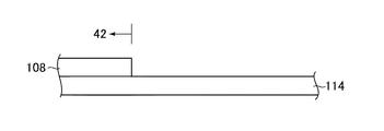
図4は、図2のI−I断面の一例を示す概略図であり、表示領域42と額縁領域44との境界部分の一例を拡大して示す図である。額縁領域44は、表示領域42を囲む領域であり、表示領域42と比較して、例えば、OLED6を含まない点で異なっている。なお、図4においては、図3に示す基材70から配線116までの層を基板114と、層間絶縁膜92から封止層106より下に配置される構造を下部構造層108と簡略化して示している。
FIG. 4 is a schematic view showing an example of the I-I cross section of FIG. 2, and is an enlarged view showing an example of the boundary portion between the
図4に示すように、例えば、封止層106内への水分の侵入を防止する観点から、樹脂材料層160の上面および端面は第3無機材料膜163に覆われており、封止層106の端部では、樹脂材料層160は存在せず、第1無機材料膜(SiNy膜)161と第3無機材料膜(SiNy膜)163とが直に接している。第2無機材料膜(SiOx膜)162の端部は樹脂材料層160よりも外方に延出しており、樹脂材料層160と第1無機材料膜161との接触を低減して、封止層106端部においても密着性を向上させている。
As shown in FIG. 4, for example, from the viewpoint of preventing the intrusion of moisture into the
第2無機材料膜162の端部(樹脂材料層160よりも外方に延び出た延出部)は、第3無機材料膜163に覆われており、第2無機材料膜162は封止層106内部に収容され、封止層106の表面には露出していない。このような構成によれば、例えば、封止層106内への水分の侵入を防止することができる。
The end portion of the second inorganic material film 162 (extending portion extending outward from the resin material layer 160) is covered with the third
第1無機材料膜161と第3無機材料膜163とが直に接触して積層された積層部の端面(封止層106の端面)の傾斜は、第2無機材料膜162の端面の傾斜よりも急峻である。
The inclination of the end face (end face of the sealing layer 106) of the laminated portion in which the first
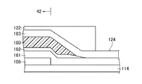
図5A〜図5Gは、実施形態に係る有機EL表示装置の製造工程例を示す図である。なお、図5においては、図3に示す基材70から配線116までの層を基板114と、層間絶縁膜92から封止層106より下に配置される構造を下部構造層108と簡略化して示している。
5A to 5G are diagrams showing an example of a manufacturing process of the organic EL display device according to the embodiment. In FIG. 5, the layer from the
図5Aは、基板114(基材70)上に、OLED6までを含む下部構造層108の形成が完了した状態を示している。次に、図5Bに示すように、基板114の表示領域42全体を覆うように第1無機材料膜161をCVD法により形成する。その際、所定の領域に第1無機材料膜161が形成されないようにマスクするマスク材は配置しない。したがって、第1無機材料膜161は、後に端子部118が形成される箇所にも形成される。
FIG. 5A shows a state in which the formation of the
図5Cは、第2無機材料膜162を形成する工程を示している。第1無機材料膜161とは異なり、後に端子部118が形成される箇所には第2無機材料膜162が形成されないように、マスク材120を所定の位置に配置し、第2無機材料膜162をCVD法により形成する。ここで、図示するように、マスク材120の内側に回り込んで第2無機材料膜162が形成され得るため、この回り込み量(例えば、内側に200μm程度)を考慮してマスク材120を配置する。第2無機材料膜162の端部は、マスク材120の内側への回り込み部に相当し、その上面は緩やかな傾斜を有している。
FIG. 5C shows a step of forming the second
図5Dは、樹脂材料層160を形成する工程を示している。樹脂材料層160は表示領域42において形成され、表示領域42において平坦化膜として機能し得る。ここでは、樹脂材料層160は、その外縁が、第2無機材料膜162の外縁よりも表示領域42側に位置するように形成されている。
FIG. 5D shows a process of forming the
図5Eは、第3無機材料膜163を形成する工程を示している。第3無機材料膜163は、基板114の表示領域42全体を覆うようにCVD法により形成する。第2無機材料膜162および樹脂材料層160は、第2無機材料膜162および樹脂材料層160の外縁よりも外側で第1無機材料膜161と第3無機材料膜163とが密着することによって封止されている。
FIG. 5E shows a step of forming the third
図5Fは、保護膜122を形成する工程を示している。ここで、保護膜122は表示領域42を覆うように形成され、保護膜122の外縁は、端子部118が形成される箇所よりも表示領域42側に位置している。保護膜122は、例えば、有機材料(代表的には、樹脂材料)で形成される。具体的には、感光性樹脂組成物を用いたパターン形成、インクジェット方式による樹脂組成物の塗布による形成、フィルムの貼付などにより保護膜122を設ける。保護膜122は、例えば、表示領域42における平坦度を向上させるとともに、次工程の周辺部124の除去に利用される。
FIG. 5F shows a step of forming the
図5Gは、周辺部124を除去する(端子出し)工程を示している。周辺部124の除去は、保護膜122をマスクとして、エッチング(例えば、ドライエッチング)により行われる。2層の無機材料膜161,163は、保護膜122の外縁の位置で切断され、端子部118が形成される。第1無機材料膜161と第3無機材料膜163とが直に接触して積層された積層部の端面1sの傾斜は、例えば、第2無機材料膜162の端面2sの傾斜よりも急峻となる。なお、周辺部124を除去した後、保護膜122を除去(図4に示す状態に)してもよいし、そのまま残して表示パネル40の保護層として用いてもよい。
FIG. 5G shows a step of removing the peripheral portion 124 (terminaling). The
図6は、図2のI−I断面の変形例を示す概略図である。上記実施形態に限られず、図6に示されるように、第2無機材料膜162は、その外縁が、樹脂材料層160の外縁よりも表示領域42側に位置するように形成されてもよい。端子部118(ドライエッチングを行う領域)と表示領域42との距離が短い設計の場合は、上述の第2無機材料膜162の形成時に用いるマスク材の内側への回り込み量を見込んで、このような形態が採用され得る。
FIG. 6 is a schematic view showing a modified example of the I-I cross section of FIG. Not limited to the above embodiment, as shown in FIG. 6, the second
本発明は、上記実施形態に限定されるものではなく、種々の変形が可能である。例えば、上記実施形態で示した構成と実質的に同一の構成、同一の作用効果を奏する構成または同一の目的を達成することができる構成で置き換えることができる。 The present invention is not limited to the above embodiment, and various modifications are possible. For example, it can be replaced with a configuration that is substantially the same as the configuration shown in the above embodiment, a configuration that exhibits the same action and effect, or a configuration that can achieve the same purpose.
本発明の思想の範疇において、当業者であれば、各種の変更例及び修正例に想到し得るものであり、それら変更例及び修正例についても本発明の範囲に属するものと了解される。例えば、前述の各実施形態に対して、当業者が適宜、構成要素の追加、削除若しくは設計変更を行ったもの、又は、工程の追加、省略若しくは条件変更を行ったものも、本発明の要旨を備えている限り、本発明の範囲に含まれる。 In the scope of the idea of the present invention, those skilled in the art can come up with various modified examples and modified examples, and it is understood that these modified examples and modified examples also belong to the scope of the present invention. For example, a person skilled in the art appropriately adds, deletes, or changes the design of each of the above-described embodiments, or adds, omits, or changes the conditions of the process, which is the gist of the present invention. Is included in the scope of the present invention as long as it is provided.
2 有機EL表示装置、4 画素アレイ部、6 OLED、8 画素回路、10 スイッチングTFT、12 駆動TFT、14 キャパシタ、20 走査線駆動回路、22 映像線駆動回路、24 駆動電源回路、26 制御装置、28 走査信号線、30 映像信号線、32 駆動電源線、40 表示パネル、42 表示領域、44 額縁領域、46 部品実装領域、48 ドライバIC、50 FPC、70 基材、72 TFT、74 回路層、80 下地層、82 半導体領域、84 ゲート絶縁膜、86 ゲート電極、88 層間絶縁層、90a ソース電極、90b ドレイン電極、92 層間絶縁膜、94 配線、96 平坦化膜、98 パッシベーション膜、100 下部電極、102 有機材料層、104 上部電極、106 封止層、108 下部構造層、110 コンタクトホール、112 バンク、114 基板、116 配線、118 端子部、120 マスク材、122 保護膜、124 周辺部、160 樹脂材料層、161 第1無機材料膜、162 第2無機材料膜、163 第3無機材料膜。 2 Organic EL display device, 4 pixel array section, 6 OLED, 8 pixel circuit, 10 switching TFT, 12 drive TFT, 14 capacitor, 20 scan line drive circuit, 22 video line drive circuit, 24 drive power supply circuit, 26 control device, 28 scanning signal line, 30 video signal line, 32 drive power supply line, 40 display panel, 42 display area, 44 frame area, 46 component mounting area, 48 driver IC, 50 FPC, 70 base material, 72 TFT, 74 circuit layer, 80 Underlayer, 82 Semiconductor Region, 84 Gate Insulating Film, 86 Gate Electrode, 88 Interlayer Insulation Layer, 90a Source Electrode, 90b Drain Electrode, 92 Interlayer Insulation Film, 94 Wiring, 96 Flattening Film, 98 Passion Film, 100 Bottom Electrode , 102 organic material layer, 104 upper electrode, 106 sealing layer, 108 lower structure layer, 110 contact hole, 112 bank, 114 substrate, 116 wiring, 118 terminal part, 120 mask material, 122 protective film, 124 peripheral part, 160 Resin material layer, 161 first inorganic material film, 162 second inorganic material film, 163 third inorganic material film.
Claims (11)
前記基板の前記表示領域に位置する複数の画素と、
前記複数の画素を覆う封止層と、を有し、
前記封止層は、前記画素が配置される側から、第1無機材料膜、第2無機材料膜、樹脂材料層および第3無機材料膜をこの順で含み、
前記第2無機材料膜は、前記樹脂材料層に接し、前記第1無機材料膜とは異なる組成を有し、前記第1無機材料膜よりも酸素元素の含有割合が高く、
前記第2無機材料膜は、前記表示領域を覆い、
前記第2無機材料膜の一部は、前記表示領域の外側に位置し、
前記第2無機材料膜の外縁は、前記樹脂材料層の外縁よりも前記表示領域側に位置する、
有機EL表示装置。 A board having a display area for displaying an image and
A plurality of pixels located in the display area of the substrate and
It has a sealing layer that covers the plurality of pixels, and has.
The sealing layer includes a first inorganic material film, a second inorganic material film, a resin material layer, and a third inorganic material film in this order from the side on which the pixels are arranged.
Said second inorganic material layer, the resin material layer in contact, have a different composition from that of the first inorganic material film, the content of oxygen element than the first inorganic material film is rather high,
The second inorganic material film covers the display area and covers the display area.
A part of the second inorganic material film is located outside the display area and is located outside the display area.
The outer edge of the second inorganic material film is located closer to the display region than the outer edge of the resin material layer.
Organic EL display device.
前記基板の前記表示領域に位置する複数の画素と、
前記複数の画素を覆う封止層と、を有し、
前記封止層は、前記画素が配置される側から、第1無機材料膜、第2無機材料膜、樹脂材料層および第3無機材料膜をこの順で含み、
前記第2無機材料膜は、前記樹脂材料層に接し、前記第1無機材料膜とは異なる組成を有し、前記第1無機材料膜よりも酸素元素の含有割合が高く、
前記第1無機材料膜、前記樹脂材料層および前記第3無機材料膜は、前記表示領域を覆い、
前記第1無機材料膜の一部は、前記表示領域の外側に位置し、
前記第3無機材料膜の一部は、前記表示領域の外側に位置し、
前記樹脂材料層の外縁及び前記第2無機材料膜の外縁よりも外側で前記第1無機材料膜と前記第3無機材料膜とが接して積層された積層部が形成されている、
有機EL表示装置。 A board having a display area for displaying an image and
A plurality of pixels located in the display area of the substrate and
It has a sealing layer that covers the plurality of pixels, and has.
The sealing layer includes a first inorganic material film, a second inorganic material film, a resin material layer, and a third inorganic material film in this order from the side on which the pixels are arranged.
The second inorganic material film is in contact with the resin material layer, has a composition different from that of the first inorganic material film, and has a higher oxygen element content than the first inorganic material film.
The first inorganic material film, the resin material layer, and the third inorganic material film cover the display area.
A part of the first inorganic material film is located outside the display area and is located outside the display area.
A part of the third inorganic material film is located outside the display area and is located outside the display area.
A laminated portion in which the first inorganic material film and the third inorganic material film are in contact with each other is formed outside the outer edge of the resin material layer and the outer edge of the second inorganic material film .
Organic EL display device.
前記第2無機材料膜の一部は、前記表示領域の外側に位置し、
前記第2無機材料膜の外縁は、前記樹脂材料層の外縁よりも外側に位置する、
請求項3に記載の有機EL表示装置。 The second inorganic material film covers the display area and covers the display area.
A part of the second inorganic material film is located outside the display area and is located outside the display area.
The outer edge of the second inorganic material film is located outside the outer edge of the resin material layer.
The organic EL display device according to claim 3.
前記第2無機材料膜の一部は、前記表示領域の外側に位置し、
前記第2無機材料膜の外縁は、前記樹脂材料層の外縁よりも前記表示領域側に位置する、
請求項3に記載の有機EL表示装置。 The second inorganic material film covers the display area and covers the display area.
A part of the second inorganic material film is located outside the display area and is located outside the display area.
The outer edge of the second inorganic material film is located closer to the display region than the outer edge of the resin material layer.
The organic EL display device according to claim 3.
請求項2から5のいずれかに記載の有機EL表示装置。 The inclination of the end face of the front miracle layer portion is steeper than the slope of the end face of the second inorganic material film,
The organic EL display device according to any one of claims 2 to 5.
請求項2から6のいずれかに記載の有機EL表示装置。 Adjacent the outer edge of the front miracle layer portion, a region where the wiring is exposed contained in the substrate is formed,
The organic EL display device according to any one of claims 2 to 6.
Priority Applications (4)
| Application Number | Priority Date | Filing Date | Title |
|---|---|---|---|
| JP2018020264A JP6983084B2 (en) | 2018-02-07 | 2018-02-07 | Organic EL display device |
| PCT/JP2018/042123 WO2019155711A1 (en) | 2018-02-07 | 2018-11-14 | Organic el display device |
| CN201880088823.0A CN111699757A (en) | 2018-02-07 | 2018-11-14 | Organic EL display device |
| US16/942,934 US11349098B2 (en) | 2018-02-07 | 2020-07-30 | Display device with an improved sealing layer |
Applications Claiming Priority (1)
| Application Number | Priority Date | Filing Date | Title |
|---|---|---|---|
| JP2018020264A JP6983084B2 (en) | 2018-02-07 | 2018-02-07 | Organic EL display device |
Publications (2)
| Publication Number | Publication Date |
|---|---|
| JP2019139884A JP2019139884A (en) | 2019-08-22 |
| JP6983084B2 true JP6983084B2 (en) | 2021-12-17 |
Family
ID=67549583
Family Applications (1)
| Application Number | Title | Priority Date | Filing Date |
|---|---|---|---|
| JP2018020264A Active JP6983084B2 (en) | 2018-02-07 | 2018-02-07 | Organic EL display device |
Country Status (4)
| Country | Link |
|---|---|
| US (1) | US11349098B2 (en) |
| JP (1) | JP6983084B2 (en) |
| CN (1) | CN111699757A (en) |
| WO (1) | WO2019155711A1 (en) |
Families Citing this family (3)
| Publication number | Priority date | Publication date | Assignee | Title |
|---|---|---|---|---|
| TW202110184A (en) | 2019-07-30 | 2021-03-01 | 日商索尼半導體解決方案公司 | Sending device, receiving device, and communication system |
| CN110518146B (en) * | 2019-08-30 | 2022-02-25 | 京东方科技集团股份有限公司 | Thin film packaging structure and display panel |
| JP7324676B2 (en) * | 2019-09-30 | 2023-08-10 | シチズンファインデバイス株式会社 | Method for manufacturing organic EL element |
Family Cites Families (28)
| Publication number | Priority date | Publication date | Assignee | Title |
|---|---|---|---|---|
| JP4624309B2 (en) * | 2006-01-24 | 2011-02-02 | 三星モバイルディスプレイ株式會社 | Organic electroluminescent display device and manufacturing method thereof |
| KR100838082B1 (en) * | 2007-03-16 | 2008-06-16 | 삼성에스디아이 주식회사 | Oled and method for fabricating the same |
| TWI420722B (en) * | 2008-01-30 | 2013-12-21 | Osram Opto Semiconductors Gmbh | Device with encapsulation unit |
| JP2010140980A (en) * | 2008-12-10 | 2010-06-24 | Sony Corp | Functional organic substance element, and functional organic substance apparatus |
| WO2011001573A1 (en) * | 2009-06-29 | 2011-01-06 | シャープ株式会社 | Organic el display device and method for manufacturing same |
| KR101990555B1 (en) * | 2012-12-24 | 2019-06-19 | 삼성디스플레이 주식회사 | Thin film encapsulation manufacturing device and manufacturing method of thin film encapsulation |
| KR102245511B1 (en) * | 2012-12-27 | 2021-04-28 | 엘지디스플레이 주식회사 | Flexible organic light emitting display device and method for manufacturing the same |
| JP6139196B2 (en) * | 2013-03-15 | 2017-05-31 | 株式会社ジャパンディスプレイ | ORGANIC ELECTROLUMINESCENT DISPLAY DEVICE AND METHOD FOR PRODUCING ORGANIC ELECTROLUMINESCENT DISPLAY DEVICE |
| KR102129035B1 (en) * | 2013-08-01 | 2020-07-02 | 삼성디스플레이 주식회사 | Organic light emitting display apparatus and the manufacturing method thereof |
| JP6374188B2 (en) | 2014-03-14 | 2018-08-15 | 東京エレクトロン株式会社 | Method for forming sealing structure, manufacturing apparatus for sealing structure, manufacturing method for organic EL element structure, and manufacturing apparatus therefor |
| JP6453579B2 (en) | 2014-08-08 | 2019-01-16 | 株式会社ジャパンディスプレイ | Organic EL display device |
| EP3002799B1 (en) * | 2014-09-30 | 2023-09-13 | LG Display Co., Ltd. | Flexible organic light emitting display device |
| KR102250584B1 (en) * | 2014-10-31 | 2021-05-10 | 엘지디스플레이 주식회사 | Organic light emitting display device |
| US20160322603A1 (en) * | 2015-04-30 | 2016-11-03 | EverDisplay Optonics (Shanghai) Limited | Display structure and manufacturing method of display device |
| JP2017083517A (en) * | 2015-10-23 | 2017-05-18 | 株式会社ジャパンディスプレイ | Display device and manufacturing method of the same |
| KR102461970B1 (en) * | 2015-11-27 | 2022-10-31 | 엘지디스플레이 주식회사 | Organic light emitting display device |
| CN105679961A (en) * | 2016-01-26 | 2016-06-15 | 京东方科技集团股份有限公司 | OLED packaging structure, display device and packaging method |
| JP6792950B2 (en) * | 2016-03-17 | 2020-12-02 | 株式会社ジャパンディスプレイ | Display device |
| JP2017174641A (en) | 2016-03-24 | 2017-09-28 | 株式会社ジャパンディスプレイ | Manufacturing method for display device |
| CN105895827B (en) * | 2016-06-28 | 2017-11-07 | 京东方科技集团股份有限公司 | A kind of organic light emitting display and its method for packing, display device |
| CN107565032A (en) * | 2016-06-30 | 2018-01-09 | 张家港保税区冠祥贸易有限公司 | A kind of organic light-emitting display device |
| JP2018014200A (en) | 2016-07-20 | 2018-01-25 | キヤノン株式会社 | Method for manufacturing organic electronics device |
| JP2018018740A (en) * | 2016-07-29 | 2018-02-01 | 株式会社ジャパンディスプレイ | Display device and manufacturing method of display device |
| JP6706999B2 (en) * | 2016-08-30 | 2020-06-10 | 株式会社ジャパンディスプレイ | Display device |
| CN106711176B (en) * | 2016-12-15 | 2019-08-23 | 上海天马有机发光显示技术有限公司 | A kind of organic light emitting display panel and preparation method thereof |
| CN106684259B (en) * | 2017-01-18 | 2018-08-14 | 深圳市华星光电技术有限公司 | OLED encapsulation method and OLED encapsulating structures |
| CN107369776B (en) * | 2017-08-18 | 2020-05-08 | 京东方科技集团股份有限公司 | Packaging structure of OLED device and OLED device |
| US10446790B2 (en) * | 2017-11-01 | 2019-10-15 | Shenzhen China Star Optoelectronics Semiconductor Display Technology Co., Ltd. | OLED encapsulating structure and manufacturing method thereof |
-
2018
- 2018-02-07 JP JP2018020264A patent/JP6983084B2/en active Active
- 2018-11-14 CN CN201880088823.0A patent/CN111699757A/en active Pending
- 2018-11-14 WO PCT/JP2018/042123 patent/WO2019155711A1/en active Application Filing
-
2020
- 2020-07-30 US US16/942,934 patent/US11349098B2/en active Active
Also Published As
| Publication number | Publication date |
|---|---|
| US11349098B2 (en) | 2022-05-31 |
| US20200381663A1 (en) | 2020-12-03 |
| CN111699757A (en) | 2020-09-22 |
| WO2019155711A1 (en) | 2019-08-15 |
| JP2019139884A (en) | 2019-08-22 |
Similar Documents
| Publication | Publication Date | Title |
|---|---|---|
| US10204846B2 (en) | Display device | |
| TWI546953B (en) | Flexible display device | |
| JP6397654B2 (en) | Organic EL light emitting device | |
| JP2016031499A (en) | Display device | |
| JP6872343B2 (en) | Display device and manufacturing method of display device | |
| US11349098B2 (en) | Display device with an improved sealing layer | |
| US10608070B2 (en) | Organic EL display device | |
| US10910464B2 (en) | Electronic device including an IC | |
| JP2020109452A (en) | Display device and manufacturing method for display device | |
| JP2018116236A (en) | Display divice | |
| JP2019179696A (en) | Organic el display and method for manufacturing organic el display | |
| KR20180003363A (en) | Organic light emitting display device | |
| JP2019003040A (en) | Display | |
| US11094759B2 (en) | Display device and method of manufacturing display device | |
| WO2019171878A1 (en) | Organic el display device | |
| JP2020027883A (en) | Organic el display and method for manufacturing organic el display | |
| WO2021053955A1 (en) | Display device and method of manufacturing display device | |
| JP6817862B2 (en) | Display device | |
| WO2019188116A1 (en) | Organic el display device and method for producing organic el display device | |
| JP2021060612A (en) | Element substrate | |
| JP2021057276A (en) | Display device | |
| KR20210085234A (en) | Organic light emitting displays device | |
| KR20190073059A (en) | Organic light emitting display device |
Legal Events
| Date | Code | Title | Description |
|---|---|---|---|
| A621 | Written request for application examination |
Free format text: JAPANESE INTERMEDIATE CODE: A621 Effective date: 20210202 |
|
| A131 | Notification of reasons for refusal |
Free format text: JAPANESE INTERMEDIATE CODE: A131 Effective date: 20210817 |
|
| A521 | Request for written amendment filed |
Free format text: JAPANESE INTERMEDIATE CODE: A523 Effective date: 20211011 |
|
| TRDD | Decision of grant or rejection written | ||
| A01 | Written decision to grant a patent or to grant a registration (utility model) |
Free format text: JAPANESE INTERMEDIATE CODE: A01 Effective date: 20211026 |
|
| A61 | First payment of annual fees (during grant procedure) |
Free format text: JAPANESE INTERMEDIATE CODE: A61 Effective date: 20211122 |
|
| R150 | Certificate of patent or registration of utility model |
Ref document number: 6983084 Country of ref document: JP Free format text: JAPANESE INTERMEDIATE CODE: R150 |