JP6981052B2 - 調光装置 - Google Patents
調光装置 Download PDFInfo
- Publication number
- JP6981052B2 JP6981052B2 JP2017113443A JP2017113443A JP6981052B2 JP 6981052 B2 JP6981052 B2 JP 6981052B2 JP 2017113443 A JP2017113443 A JP 2017113443A JP 2017113443 A JP2017113443 A JP 2017113443A JP 6981052 B2 JP6981052 B2 JP 6981052B2
- Authority
- JP
- Japan
- Prior art keywords
- voltage
- terminal
- period
- drive
- liquid crystal
- Prior art date
- Legal status (The legal status is an assumption and is not a legal conclusion. Google has not performed a legal analysis and makes no representation as to the accuracy of the status listed.)
- Active
Links
Images


Classifications
-
- G—PHYSICS
- G02—OPTICS
- G02F—OPTICAL DEVICES OR ARRANGEMENTS FOR THE CONTROL OF LIGHT BY MODIFICATION OF THE OPTICAL PROPERTIES OF THE MEDIA OF THE ELEMENTS INVOLVED THEREIN; NON-LINEAR OPTICS; FREQUENCY-CHANGING OF LIGHT; OPTICAL LOGIC ELEMENTS; OPTICAL ANALOGUE/DIGITAL CONVERTERS
- G02F1/00—Devices or arrangements for the control of the intensity, colour, phase, polarisation or direction of light arriving from an independent light source, e.g. switching, gating or modulating; Non-linear optics
- G02F1/01—Devices or arrangements for the control of the intensity, colour, phase, polarisation or direction of light arriving from an independent light source, e.g. switching, gating or modulating; Non-linear optics for the control of the intensity, phase, polarisation or colour
- G02F1/13—Devices or arrangements for the control of the intensity, colour, phase, polarisation or direction of light arriving from an independent light source, e.g. switching, gating or modulating; Non-linear optics for the control of the intensity, phase, polarisation or colour based on liquid crystals, e.g. single liquid crystal display cells
- G02F1/133—Constructional arrangements; Operation of liquid crystal cells; Circuit arrangements
- G02F1/13306—Circuit arrangements or driving methods for the control of single liquid crystal cells
-
- G—PHYSICS
- G02—OPTICS
- G02F—OPTICAL DEVICES OR ARRANGEMENTS FOR THE CONTROL OF LIGHT BY MODIFICATION OF THE OPTICAL PROPERTIES OF THE MEDIA OF THE ELEMENTS INVOLVED THEREIN; NON-LINEAR OPTICS; FREQUENCY-CHANGING OF LIGHT; OPTICAL LOGIC ELEMENTS; OPTICAL ANALOGUE/DIGITAL CONVERTERS
- G02F1/00—Devices or arrangements for the control of the intensity, colour, phase, polarisation or direction of light arriving from an independent light source, e.g. switching, gating or modulating; Non-linear optics
- G02F1/01—Devices or arrangements for the control of the intensity, colour, phase, polarisation or direction of light arriving from an independent light source, e.g. switching, gating or modulating; Non-linear optics for the control of the intensity, phase, polarisation or colour
- G02F1/13—Devices or arrangements for the control of the intensity, colour, phase, polarisation or direction of light arriving from an independent light source, e.g. switching, gating or modulating; Non-linear optics for the control of the intensity, phase, polarisation or colour based on liquid crystals, e.g. single liquid crystal display cells
- G02F1/133—Constructional arrangements; Operation of liquid crystal cells; Circuit arrangements
- G02F1/1333—Constructional arrangements; Manufacturing methods
- G02F1/1334—Constructional arrangements; Manufacturing methods based on polymer dispersed liquid crystals, e.g. microencapsulated liquid crystals
-
- G—PHYSICS
- G02—OPTICS
- G02F—OPTICAL DEVICES OR ARRANGEMENTS FOR THE CONTROL OF LIGHT BY MODIFICATION OF THE OPTICAL PROPERTIES OF THE MEDIA OF THE ELEMENTS INVOLVED THEREIN; NON-LINEAR OPTICS; FREQUENCY-CHANGING OF LIGHT; OPTICAL LOGIC ELEMENTS; OPTICAL ANALOGUE/DIGITAL CONVERTERS
- G02F1/00—Devices or arrangements for the control of the intensity, colour, phase, polarisation or direction of light arriving from an independent light source, e.g. switching, gating or modulating; Non-linear optics
- G02F1/01—Devices or arrangements for the control of the intensity, colour, phase, polarisation or direction of light arriving from an independent light source, e.g. switching, gating or modulating; Non-linear optics for the control of the intensity, phase, polarisation or colour
- G02F1/13—Devices or arrangements for the control of the intensity, colour, phase, polarisation or direction of light arriving from an independent light source, e.g. switching, gating or modulating; Non-linear optics for the control of the intensity, phase, polarisation or colour based on liquid crystals, e.g. single liquid crystal display cells
- G02F1/133—Constructional arrangements; Operation of liquid crystal cells; Circuit arrangements
- G02F1/1333—Constructional arrangements; Manufacturing methods
- G02F1/1343—Electrodes
- G02F1/13439—Electrodes characterised by their electrical, optical, physical properties; materials therefor; method of making
-
- G—PHYSICS
- G02—OPTICS
- G02F—OPTICAL DEVICES OR ARRANGEMENTS FOR THE CONTROL OF LIGHT BY MODIFICATION OF THE OPTICAL PROPERTIES OF THE MEDIA OF THE ELEMENTS INVOLVED THEREIN; NON-LINEAR OPTICS; FREQUENCY-CHANGING OF LIGHT; OPTICAL LOGIC ELEMENTS; OPTICAL ANALOGUE/DIGITAL CONVERTERS
- G02F1/00—Devices or arrangements for the control of the intensity, colour, phase, polarisation or direction of light arriving from an independent light source, e.g. switching, gating or modulating; Non-linear optics
- G02F1/01—Devices or arrangements for the control of the intensity, colour, phase, polarisation or direction of light arriving from an independent light source, e.g. switching, gating or modulating; Non-linear optics for the control of the intensity, phase, polarisation or colour
- G02F1/13—Devices or arrangements for the control of the intensity, colour, phase, polarisation or direction of light arriving from an independent light source, e.g. switching, gating or modulating; Non-linear optics for the control of the intensity, phase, polarisation or colour based on liquid crystals, e.g. single liquid crystal display cells
- G02F1/133—Constructional arrangements; Operation of liquid crystal cells; Circuit arrangements
- G02F1/1333—Constructional arrangements; Manufacturing methods
- G02F1/1345—Conductors connecting electrodes to cell terminals
-
- G—PHYSICS
- G02—OPTICS
- G02F—OPTICAL DEVICES OR ARRANGEMENTS FOR THE CONTROL OF LIGHT BY MODIFICATION OF THE OPTICAL PROPERTIES OF THE MEDIA OF THE ELEMENTS INVOLVED THEREIN; NON-LINEAR OPTICS; FREQUENCY-CHANGING OF LIGHT; OPTICAL LOGIC ELEMENTS; OPTICAL ANALOGUE/DIGITAL CONVERTERS
- G02F1/00—Devices or arrangements for the control of the intensity, colour, phase, polarisation or direction of light arriving from an independent light source, e.g. switching, gating or modulating; Non-linear optics
- G02F1/01—Devices or arrangements for the control of the intensity, colour, phase, polarisation or direction of light arriving from an independent light source, e.g. switching, gating or modulating; Non-linear optics for the control of the intensity, phase, polarisation or colour
- G02F1/13—Devices or arrangements for the control of the intensity, colour, phase, polarisation or direction of light arriving from an independent light source, e.g. switching, gating or modulating; Non-linear optics for the control of the intensity, phase, polarisation or colour based on liquid crystals, e.g. single liquid crystal display cells
- G02F1/137—Devices or arrangements for the control of the intensity, colour, phase, polarisation or direction of light arriving from an independent light source, e.g. switching, gating or modulating; Non-linear optics for the control of the intensity, phase, polarisation or colour based on liquid crystals, e.g. single liquid crystal display cells characterised by the electro-optical or magneto-optical effect, e.g. field-induced phase transition, orientation effect, guest-host interaction or dynamic scattering
- G02F1/139—Devices or arrangements for the control of the intensity, colour, phase, polarisation or direction of light arriving from an independent light source, e.g. switching, gating or modulating; Non-linear optics for the control of the intensity, phase, polarisation or colour based on liquid crystals, e.g. single liquid crystal display cells characterised by the electro-optical or magneto-optical effect, e.g. field-induced phase transition, orientation effect, guest-host interaction or dynamic scattering based on orientation effects in which the liquid crystal remains transparent
-
- G—PHYSICS
- G02—OPTICS
- G02F—OPTICAL DEVICES OR ARRANGEMENTS FOR THE CONTROL OF LIGHT BY MODIFICATION OF THE OPTICAL PROPERTIES OF THE MEDIA OF THE ELEMENTS INVOLVED THEREIN; NON-LINEAR OPTICS; FREQUENCY-CHANGING OF LIGHT; OPTICAL LOGIC ELEMENTS; OPTICAL ANALOGUE/DIGITAL CONVERTERS
- G02F1/00—Devices or arrangements for the control of the intensity, colour, phase, polarisation or direction of light arriving from an independent light source, e.g. switching, gating or modulating; Non-linear optics
- G02F1/01—Devices or arrangements for the control of the intensity, colour, phase, polarisation or direction of light arriving from an independent light source, e.g. switching, gating or modulating; Non-linear optics for the control of the intensity, phase, polarisation or colour
- G02F1/13—Devices or arrangements for the control of the intensity, colour, phase, polarisation or direction of light arriving from an independent light source, e.g. switching, gating or modulating; Non-linear optics for the control of the intensity, phase, polarisation or colour based on liquid crystals, e.g. single liquid crystal display cells
- G02F1/133—Constructional arrangements; Operation of liquid crystal cells; Circuit arrangements
- G02F1/1333—Constructional arrangements; Manufacturing methods
- G02F1/1339—Gaskets; Spacers; Sealing of cells
-
- G—PHYSICS
- G02—OPTICS
- G02F—OPTICAL DEVICES OR ARRANGEMENTS FOR THE CONTROL OF LIGHT BY MODIFICATION OF THE OPTICAL PROPERTIES OF THE MEDIA OF THE ELEMENTS INVOLVED THEREIN; NON-LINEAR OPTICS; FREQUENCY-CHANGING OF LIGHT; OPTICAL LOGIC ELEMENTS; OPTICAL ANALOGUE/DIGITAL CONVERTERS
- G02F1/00—Devices or arrangements for the control of the intensity, colour, phase, polarisation or direction of light arriving from an independent light source, e.g. switching, gating or modulating; Non-linear optics
- G02F1/01—Devices or arrangements for the control of the intensity, colour, phase, polarisation or direction of light arriving from an independent light source, e.g. switching, gating or modulating; Non-linear optics for the control of the intensity, phase, polarisation or colour
- G02F1/13—Devices or arrangements for the control of the intensity, colour, phase, polarisation or direction of light arriving from an independent light source, e.g. switching, gating or modulating; Non-linear optics for the control of the intensity, phase, polarisation or colour based on liquid crystals, e.g. single liquid crystal display cells
- G02F1/137—Devices or arrangements for the control of the intensity, colour, phase, polarisation or direction of light arriving from an independent light source, e.g. switching, gating or modulating; Non-linear optics for the control of the intensity, phase, polarisation or colour based on liquid crystals, e.g. single liquid crystal display cells characterised by the electro-optical or magneto-optical effect, e.g. field-induced phase transition, orientation effect, guest-host interaction or dynamic scattering
- G02F1/13706—Devices or arrangements for the control of the intensity, colour, phase, polarisation or direction of light arriving from an independent light source, e.g. switching, gating or modulating; Non-linear optics for the control of the intensity, phase, polarisation or colour based on liquid crystals, e.g. single liquid crystal display cells characterised by the electro-optical or magneto-optical effect, e.g. field-induced phase transition, orientation effect, guest-host interaction or dynamic scattering the liquid crystal having positive dielectric anisotropy
-
- G—PHYSICS
- G02—OPTICS
- G02F—OPTICAL DEVICES OR ARRANGEMENTS FOR THE CONTROL OF LIGHT BY MODIFICATION OF THE OPTICAL PROPERTIES OF THE MEDIA OF THE ELEMENTS INVOLVED THEREIN; NON-LINEAR OPTICS; FREQUENCY-CHANGING OF LIGHT; OPTICAL LOGIC ELEMENTS; OPTICAL ANALOGUE/DIGITAL CONVERTERS
- G02F1/00—Devices or arrangements for the control of the intensity, colour, phase, polarisation or direction of light arriving from an independent light source, e.g. switching, gating or modulating; Non-linear optics
- G02F1/01—Devices or arrangements for the control of the intensity, colour, phase, polarisation or direction of light arriving from an independent light source, e.g. switching, gating or modulating; Non-linear optics for the control of the intensity, phase, polarisation or colour
- G02F1/13—Devices or arrangements for the control of the intensity, colour, phase, polarisation or direction of light arriving from an independent light source, e.g. switching, gating or modulating; Non-linear optics for the control of the intensity, phase, polarisation or colour based on liquid crystals, e.g. single liquid crystal display cells
- G02F1/137—Devices or arrangements for the control of the intensity, colour, phase, polarisation or direction of light arriving from an independent light source, e.g. switching, gating or modulating; Non-linear optics for the control of the intensity, phase, polarisation or colour based on liquid crystals, e.g. single liquid crystal display cells characterised by the electro-optical or magneto-optical effect, e.g. field-induced phase transition, orientation effect, guest-host interaction or dynamic scattering
- G02F1/13756—Devices or arrangements for the control of the intensity, colour, phase, polarisation or direction of light arriving from an independent light source, e.g. switching, gating or modulating; Non-linear optics for the control of the intensity, phase, polarisation or colour based on liquid crystals, e.g. single liquid crystal display cells characterised by the electro-optical or magneto-optical effect, e.g. field-induced phase transition, orientation effect, guest-host interaction or dynamic scattering the liquid crystal selectively assuming a light-scattering state
Landscapes
- Physics & Mathematics (AREA)
- Nonlinear Science (AREA)
- Chemical & Material Sciences (AREA)
- Crystallography & Structural Chemistry (AREA)
- General Physics & Mathematics (AREA)
- Optics & Photonics (AREA)
- Mathematical Physics (AREA)
- Dispersion Chemistry (AREA)
- Liquid Crystal (AREA)
- Control Of Indicators Other Than Cathode Ray Tubes (AREA)
Description
[1] 調光装置10の構成
図1は、本発明の第1実施形態に係る調光装置10のブロック図である。調光装置10は、調光素子11、駆動回路12、電源回路13、及び制御回路14を備える。
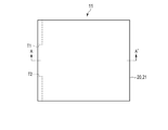
次に、調光素子11の構成について説明する。図2は、調光素子11の平面図である。図3は、図2のA−A´線に沿った調光素子11の断面図である。
次に、液晶層(調光層)24の大まかな動作について説明する。
次に、調光素子11の等価回路について説明する。図5は、調光素子11の等価回路図である。
次に、駆動回路12の構成について説明する。図6は、駆動回路12を主として示した回路図である。
上記のように構成された調光装置10の動作について説明する。図7は、制御回路14の動作を説明するタイミング図である。前述したように、制御回路14は、信号OVPOSIN、信号CONPOSIN、信号OVNEGIN、及び信号CONNEGINを生成する。
次に、比較例に係る調光装置について説明する。図10は、比較例に係る駆動回路の回路図である。
以上詳述したように第1実施形態では、調光装置10は、対向配置された基材20、21と、基材20、21にそれぞれ設けられた透明電極22、23と、透明電極22、23間に充填された液晶層24と、透明電極22、23に電気的に接続された端子T1、T2とを含む調光素子11と、端子T1に駆動電圧OUT1を印加し、端子T2に駆動電圧OUT1と極性が異なる駆動電圧OUT2を印加する駆動回路12とを具備する。駆動電圧OUT1は、第1期間において正側オーバードライブ電圧Vov+に設定され、前記第1期間に続く第2期間において正側制御電圧Vc+に設定され、第2期間に続く第3期間において負側オーバードライブ電圧Vov−に設定され、第3期間に続く第4期間において負側制御電圧Vc−に設定される。
第2実施形態は、駆動回路12、及び電源回路13の具体的な構成例である。第2実施形態は、トランジスタを用いてデジタル式に駆動回路12を構成した例である。
第3実施形態は、駆動回路12、及び電源回路13の具体的な構成例である。第3実施形態は、電力増幅器を用いてアナログ式に駆動回路12を構成した例である。
上記実施形態では、PDLC又はPNLCを用いた液晶素子(調光素子)を例示しているが、これに限定されるものではない。調光素子としての液晶素子は、偏光板及び配向膜を液晶層の両側に配置した構成でもよく、TN(Twisted Nematic)方式、VA(Vertical Alignment)方式、又はIPS(In-Plane Switching)方式などを用いることができる。また、調光素子として、液晶素子以外で、電圧により屈折率が変化する様々な種類の電気光学素子を用いることができる。
Claims (8)
- 第1及び第2基材と、前記第1基材上に平面状に設けられた第1電極と、前記第2基材上に平面状に設けられた第2電極と、前記第1及び第2電極間に充填されかつ高分子分散型又はポリマーネットワーク型の液晶層と、前記第1及び第2電極に電気的に接続された第1及び第2端子とを含む調光素子と、
前記第1端子に第1駆動電圧を印加し、前記第2端子に前記第1駆動電圧と極性が異なる第2駆動電圧を印加する駆動回路と
を具備し、
前記第1駆動電圧は、第1期間において第1電圧に設定され、前記第1期間に続く第2期間において前記第1電圧より低い第2電圧に設定され、前記第2期間に続く第3期間において前記第2電圧より低い第3電圧に設定され、前記第3期間に続く第4期間において前記第2電圧より低くかつ前記第3電圧より高い第4電圧に設定され、
前記第2駆動電圧は、前記第1期間において前記第3電圧に設定され、前記第2期間において前記第4電圧に設定され、前記第3期間において前記第1電圧に設定され、前記第4期間において前記第2電圧に設定され、
前記第1電圧と前記第3電圧との電圧差は、前記調光素子の耐圧より小さい
調光装置。 - 前記第2電圧と前記第4電圧との電圧差は、前記調光素子の飽和電圧以下である
請求項1に記載の調光装置。 - 前記第2電圧と前記第4電圧との電圧差は、前記液晶層の閾値電圧以上である
請求項1又は2に記載の調光装置。 - 前記第1期間は、前記第1電極のうち前記第1端子から最も離れた末端側の電圧が前記第4電圧から前記第2電圧に立ち上がる期間より短く設定され、
前記第3期間は、前記末端側の電圧が前記第2電圧から前記第4電圧に立ち下がる期間より短く設定される
請求項1乃至3のいずれかに記載の調光装置。 - 前記駆動回路は、第1乃至第8スイッチング素子を含み、
前記第1スイッチング素子は、前記第1電圧を発生する第1電圧源と前記第1端子との間に接続され、
前記第2スイッチング素子は、前記第3電圧を発生する第3電圧源と前記第1端子との間に接続され、
前記第3スイッチング素子は、前記第1電圧源と前記第2端子との間に接続され、
前記第4スイッチング素子は、前記第3電圧源と前記第2端子との間に接続され、
前記第5スイッチング素子は、前記第2電圧を発生する第2電圧源と前記第1端子との間に接続され、
前記第6スイッチング素子は、前記第4電圧を発生する第4電圧源と前記第1端子との間に接続され、
前記第7スイッチング素子は、前記第2電圧源と前記第2端子との間に接続され、
前記第8スイッチング素子は、前記第4電圧源と前記第2端子との間に接続される
請求項1乃至4のいずれかに記載の調光装置。 - 第1乃至第4制御信号を生成する制御回路をさらに具備し、
前記第1制御信号は、前記第1及び第4スイッチング素子に入力され、
前記第2制御信号は、前記第2及び第3スイッチング素子に入力され、
前記第3制御信号は、前記第5及び第8スイッチング素子に入力され、
前記第4制御信号は、前記第6及び第7スイッチング素子に入力される
請求項5に記載の調光装置。 - 前記第1乃至第4電圧源の各々は、定電圧素子を含む
請求項5又は6に記載の調光装置。 - 前記第1乃至第8スイッチング素子の各々は、トランジスタで構成される
請求項5乃至7のいずれかに記載の調光装置。
Priority Applications (6)
| Application Number | Priority Date | Filing Date | Title |
|---|---|---|---|
| JP2017113443A JP6981052B2 (ja) | 2017-06-08 | 2017-06-08 | 調光装置 |
| EP18812822.7A EP3637176B1 (en) | 2017-06-08 | 2018-05-31 | Light control device |
| CN201880035752.8A CN110678805B (zh) | 2017-06-08 | 2018-05-31 | 调光装置 |
| PCT/JP2018/021054 WO2018225625A1 (ja) | 2017-06-08 | 2018-05-31 | 調光装置 |
| US16/704,526 US10871668B2 (en) | 2017-06-08 | 2019-12-05 | Light control device |
| JP2021187781A JP7226510B2 (ja) | 2017-06-08 | 2021-11-18 | 調光装置 |
Applications Claiming Priority (1)
| Application Number | Priority Date | Filing Date | Title |
|---|---|---|---|
| JP2017113443A JP6981052B2 (ja) | 2017-06-08 | 2017-06-08 | 調光装置 |
Related Child Applications (1)
| Application Number | Title | Priority Date | Filing Date |
|---|---|---|---|
| JP2021187781A Division JP7226510B2 (ja) | 2017-06-08 | 2021-11-18 | 調光装置 |
Publications (3)
| Publication Number | Publication Date |
|---|---|
| JP2018205631A JP2018205631A (ja) | 2018-12-27 |
| JP2018205631A5 JP2018205631A5 (ja) | 2020-08-13 |
| JP6981052B2 true JP6981052B2 (ja) | 2021-12-15 |
Family
ID=64565864
Family Applications (1)
| Application Number | Title | Priority Date | Filing Date |
|---|---|---|---|
| JP2017113443A Active JP6981052B2 (ja) | 2017-06-08 | 2017-06-08 | 調光装置 |
Country Status (5)
| Country | Link |
|---|---|
| US (1) | US10871668B2 (ja) |
| EP (1) | EP3637176B1 (ja) |
| JP (1) | JP6981052B2 (ja) |
| CN (1) | CN110678805B (ja) |
| WO (1) | WO2018225625A1 (ja) |
Families Citing this family (3)
| Publication number | Priority date | Publication date | Assignee | Title |
|---|---|---|---|---|
| KR102018352B1 (ko) * | 2019-02-25 | 2019-10-21 | 주식회사 제이앤에스 | Haze 특성이 개선된 스마트 필름 장치 |
| JP7263938B2 (ja) * | 2019-06-20 | 2023-04-25 | 凸版印刷株式会社 | 調光シート駆動装置、調光装置、調光シートの駆動方法、および、調光シートの駆動プログラム |
| BR112023026207A2 (pt) * | 2021-06-23 | 2024-03-05 | Japan Display Inc | Dispositivo óptico |
Family Cites Families (15)
| Publication number | Priority date | Publication date | Assignee | Title |
|---|---|---|---|---|
| JPS6449924A (en) | 1987-08-20 | 1989-02-27 | Teraoka Seiko Kk | Strain gage type load cell |
| JPS6449924U (ja) * | 1987-09-24 | 1989-03-28 | ||
| JPH10197849A (ja) * | 1997-01-06 | 1998-07-31 | Matsushita Electric Ind Co Ltd | 反強誘電性液晶素子の駆動方法および駆動装置 |
| TWI259992B (en) * | 2003-05-22 | 2006-08-11 | Au Optronics Corp | Liquid crystal display device driver and method thereof |
| JP2005010202A (ja) * | 2003-06-16 | 2005-01-13 | Nec Corp | 液晶パネル、該液晶パネルを用いた液晶表示装置および該液晶表示装置を搭載した電子機器 |
| TWI329214B (en) * | 2003-12-18 | 2010-08-21 | Sharp Kk | Display element and display device, driving method of display element, and program |
| WO2006030388A2 (en) * | 2004-09-15 | 2006-03-23 | Koninklijke Philips Electronics N.V. | Display devices and methods of driving such |
| TWI282544B (en) * | 2005-01-21 | 2007-06-11 | Himax Tech Inc | Operation apparatus, operation method, operation apparatus for overdrive and operation method for overdrive |
| JP4661406B2 (ja) * | 2005-07-05 | 2011-03-30 | 富士ゼロックス株式会社 | 液晶デバイスの駆動方法、および液晶デバイス駆動装置 |
| JP2007304561A (ja) * | 2006-03-23 | 2007-11-22 | Toshiba Matsushita Display Technology Co Ltd | 液晶表示装置の駆動装置 |
| JP4645632B2 (ja) * | 2007-09-21 | 2011-03-09 | ソニー株式会社 | 液晶表示装置、液晶表示装置の駆動方法および電子機器 |
| WO2009063661A1 (ja) * | 2007-11-13 | 2009-05-22 | Sharp Kabushiki Kaisha | 電源回路およびそれを備える表示装置 |
| JP2013072895A (ja) * | 2011-09-26 | 2013-04-22 | Seiko Electric Co Ltd | 液晶調光装置及び液晶調光素子の駆動装置 |
| TWM494455U (zh) * | 2014-09-23 | 2015-01-21 | Unity Opto Technology Co Ltd | 改善led頻閃之驅動電路 |
| WO2018178043A1 (en) * | 2017-03-29 | 2018-10-04 | Merck Patent Gmbh | Method for electrically driving a switchable optical element |
-
2017
- 2017-06-08 JP JP2017113443A patent/JP6981052B2/ja active Active
-
2018
- 2018-05-31 CN CN201880035752.8A patent/CN110678805B/zh active Active
- 2018-05-31 EP EP18812822.7A patent/EP3637176B1/en active Active
- 2018-05-31 WO PCT/JP2018/021054 patent/WO2018225625A1/ja unknown
-
2019
- 2019-12-05 US US16/704,526 patent/US10871668B2/en active Active
Also Published As
| Publication number | Publication date |
|---|---|
| EP3637176B1 (en) | 2024-04-24 |
| CN110678805A (zh) | 2020-01-10 |
| CN110678805B (zh) | 2022-08-23 |
| US10871668B2 (en) | 2020-12-22 |
| JP2018205631A (ja) | 2018-12-27 |
| WO2018225625A1 (ja) | 2018-12-13 |
| EP3637176A1 (en) | 2020-04-15 |
| US20200110297A1 (en) | 2020-04-09 |
| EP3637176A4 (en) | 2020-06-10 |
Similar Documents
| Publication | Publication Date | Title |
|---|---|---|
| JP6733747B2 (ja) | 調光装置 | |
| US10871668B2 (en) | Light control device | |
| JP5188362B2 (ja) | バックライトユニットの光源駆動装置及び方法 | |
| KR20120110387A (ko) | 화소 회로 및 화소 회로의 구동 방법 | |
| CN110428785A (zh) | Tft面板控制电路 | |
| TW202145191A (zh) | 使用脈衝寬度調變產生器之畫素電路和顯示裝置 | |
| KR20100006320A (ko) | 백라이트 유닛의 광원 구동장치 및 방법 | |
| CN102930841A (zh) | 近晶态液晶多稳态电子纸显示器的像素电路 | |
| US10971106B2 (en) | Liquid crystal optical modulation device and liquid crystal optical modulation method | |
| WO2018186447A1 (ja) | 液晶調光装置及び液晶調光方法 | |
| JP6836010B2 (ja) | 直流電圧変換回路及び直流電圧変換方法並びに液晶表示装置 | |
| JP7226510B2 (ja) | 調光装置 | |
| US20090073156A1 (en) | Drive Circuits for Capacitive Loads | |
| KR101660979B1 (ko) | 액정표시장치 | |
| RU2653769C1 (ru) | Жидкокристаллическая 3d панель с технологией "невооруженным глазом" и способ управления такой панелью | |
| KR100600693B1 (ko) | 액정 표시 소자의 구동 방법 | |
| CN201765805U (zh) | 电流控制电路 | |
| KR100265782B1 (ko) | 박막트랜지스터형액정표시장치 | |
| TWI537929B (zh) | 液晶顯示器及其驅動控制電路 | |
| KR102029851B1 (ko) | 라이트 구동 장치 및 이를 구비한 액정 표시 장치 | |
| KR20070071338A (ko) | 평판표시장치용 인버터 구동방법 |
Legal Events
| Date | Code | Title | Description |
|---|---|---|---|
| A711 | Notification of change in applicant |
Free format text: JAPANESE INTERMEDIATE CODE: A712 Effective date: 20190425 |
|
| A621 | Written request for application examination |
Free format text: JAPANESE INTERMEDIATE CODE: A621 Effective date: 20200518 |
|
| A521 | Request for written amendment filed |
Free format text: JAPANESE INTERMEDIATE CODE: A523 Effective date: 20200630 |
|
| A131 | Notification of reasons for refusal |
Free format text: JAPANESE INTERMEDIATE CODE: A131 Effective date: 20210622 |
|
| A521 | Request for written amendment filed |
Free format text: JAPANESE INTERMEDIATE CODE: A523 Effective date: 20210812 |
|
| TRDD | Decision of grant or rejection written | ||
| A01 | Written decision to grant a patent or to grant a registration (utility model) |
Free format text: JAPANESE INTERMEDIATE CODE: A01 Effective date: 20211019 |
|
| A61 | First payment of annual fees (during grant procedure) |
Free format text: JAPANESE INTERMEDIATE CODE: A61 Effective date: 20211101 |
|
| R150 | Certificate of patent or registration of utility model |
Ref document number: 6981052 Country of ref document: JP Free format text: JAPANESE INTERMEDIATE CODE: R150 |