JP6981052B2 - Dimmer - Google Patents
Dimmer Download PDFInfo
- Publication number
- JP6981052B2 JP6981052B2 JP2017113443A JP2017113443A JP6981052B2 JP 6981052 B2 JP6981052 B2 JP 6981052B2 JP 2017113443 A JP2017113443 A JP 2017113443A JP 2017113443 A JP2017113443 A JP 2017113443A JP 6981052 B2 JP6981052 B2 JP 6981052B2
- Authority
- JP
- Japan
- Prior art keywords
- voltage
- terminal
- period
- drive
- liquid crystal
- Prior art date
- Legal status (The legal status is an assumption and is not a legal conclusion. Google has not performed a legal analysis and makes no representation as to the accuracy of the status listed.)
- Active
Links
Images


Classifications
-
- G—PHYSICS
- G02—OPTICS
- G02F—OPTICAL DEVICES OR ARRANGEMENTS FOR THE CONTROL OF LIGHT BY MODIFICATION OF THE OPTICAL PROPERTIES OF THE MEDIA OF THE ELEMENTS INVOLVED THEREIN; NON-LINEAR OPTICS; FREQUENCY-CHANGING OF LIGHT; OPTICAL LOGIC ELEMENTS; OPTICAL ANALOGUE/DIGITAL CONVERTERS
- G02F1/00—Devices or arrangements for the control of the intensity, colour, phase, polarisation or direction of light arriving from an independent light source, e.g. switching, gating or modulating; Non-linear optics
- G02F1/01—Devices or arrangements for the control of the intensity, colour, phase, polarisation or direction of light arriving from an independent light source, e.g. switching, gating or modulating; Non-linear optics for the control of the intensity, phase, polarisation or colour
- G02F1/13—Devices or arrangements for the control of the intensity, colour, phase, polarisation or direction of light arriving from an independent light source, e.g. switching, gating or modulating; Non-linear optics for the control of the intensity, phase, polarisation or colour based on liquid crystals, e.g. single liquid crystal display cells
- G02F1/133—Constructional arrangements; Operation of liquid crystal cells; Circuit arrangements
- G02F1/13306—Circuit arrangements or driving methods for the control of single liquid crystal cells
-
- G—PHYSICS
- G02—OPTICS
- G02F—OPTICAL DEVICES OR ARRANGEMENTS FOR THE CONTROL OF LIGHT BY MODIFICATION OF THE OPTICAL PROPERTIES OF THE MEDIA OF THE ELEMENTS INVOLVED THEREIN; NON-LINEAR OPTICS; FREQUENCY-CHANGING OF LIGHT; OPTICAL LOGIC ELEMENTS; OPTICAL ANALOGUE/DIGITAL CONVERTERS
- G02F1/00—Devices or arrangements for the control of the intensity, colour, phase, polarisation or direction of light arriving from an independent light source, e.g. switching, gating or modulating; Non-linear optics
- G02F1/01—Devices or arrangements for the control of the intensity, colour, phase, polarisation or direction of light arriving from an independent light source, e.g. switching, gating or modulating; Non-linear optics for the control of the intensity, phase, polarisation or colour
- G02F1/13—Devices or arrangements for the control of the intensity, colour, phase, polarisation or direction of light arriving from an independent light source, e.g. switching, gating or modulating; Non-linear optics for the control of the intensity, phase, polarisation or colour based on liquid crystals, e.g. single liquid crystal display cells
- G02F1/133—Constructional arrangements; Operation of liquid crystal cells; Circuit arrangements
- G02F1/1333—Constructional arrangements; Manufacturing methods
- G02F1/1334—Constructional arrangements; Manufacturing methods based on polymer dispersed liquid crystals, e.g. microencapsulated liquid crystals
-
- G—PHYSICS
- G02—OPTICS
- G02F—OPTICAL DEVICES OR ARRANGEMENTS FOR THE CONTROL OF LIGHT BY MODIFICATION OF THE OPTICAL PROPERTIES OF THE MEDIA OF THE ELEMENTS INVOLVED THEREIN; NON-LINEAR OPTICS; FREQUENCY-CHANGING OF LIGHT; OPTICAL LOGIC ELEMENTS; OPTICAL ANALOGUE/DIGITAL CONVERTERS
- G02F1/00—Devices or arrangements for the control of the intensity, colour, phase, polarisation or direction of light arriving from an independent light source, e.g. switching, gating or modulating; Non-linear optics
- G02F1/01—Devices or arrangements for the control of the intensity, colour, phase, polarisation or direction of light arriving from an independent light source, e.g. switching, gating or modulating; Non-linear optics for the control of the intensity, phase, polarisation or colour
- G02F1/13—Devices or arrangements for the control of the intensity, colour, phase, polarisation or direction of light arriving from an independent light source, e.g. switching, gating or modulating; Non-linear optics for the control of the intensity, phase, polarisation or colour based on liquid crystals, e.g. single liquid crystal display cells
- G02F1/133—Constructional arrangements; Operation of liquid crystal cells; Circuit arrangements
- G02F1/1333—Constructional arrangements; Manufacturing methods
- G02F1/1343—Electrodes
- G02F1/13439—Electrodes characterised by their electrical, optical, physical properties; materials therefor; method of making
-
- G—PHYSICS
- G02—OPTICS
- G02F—OPTICAL DEVICES OR ARRANGEMENTS FOR THE CONTROL OF LIGHT BY MODIFICATION OF THE OPTICAL PROPERTIES OF THE MEDIA OF THE ELEMENTS INVOLVED THEREIN; NON-LINEAR OPTICS; FREQUENCY-CHANGING OF LIGHT; OPTICAL LOGIC ELEMENTS; OPTICAL ANALOGUE/DIGITAL CONVERTERS
- G02F1/00—Devices or arrangements for the control of the intensity, colour, phase, polarisation or direction of light arriving from an independent light source, e.g. switching, gating or modulating; Non-linear optics
- G02F1/01—Devices or arrangements for the control of the intensity, colour, phase, polarisation or direction of light arriving from an independent light source, e.g. switching, gating or modulating; Non-linear optics for the control of the intensity, phase, polarisation or colour
- G02F1/13—Devices or arrangements for the control of the intensity, colour, phase, polarisation or direction of light arriving from an independent light source, e.g. switching, gating or modulating; Non-linear optics for the control of the intensity, phase, polarisation or colour based on liquid crystals, e.g. single liquid crystal display cells
- G02F1/133—Constructional arrangements; Operation of liquid crystal cells; Circuit arrangements
- G02F1/1333—Constructional arrangements; Manufacturing methods
- G02F1/1345—Conductors connecting electrodes to cell terminals
-
- G—PHYSICS
- G02—OPTICS
- G02F—OPTICAL DEVICES OR ARRANGEMENTS FOR THE CONTROL OF LIGHT BY MODIFICATION OF THE OPTICAL PROPERTIES OF THE MEDIA OF THE ELEMENTS INVOLVED THEREIN; NON-LINEAR OPTICS; FREQUENCY-CHANGING OF LIGHT; OPTICAL LOGIC ELEMENTS; OPTICAL ANALOGUE/DIGITAL CONVERTERS
- G02F1/00—Devices or arrangements for the control of the intensity, colour, phase, polarisation or direction of light arriving from an independent light source, e.g. switching, gating or modulating; Non-linear optics
- G02F1/01—Devices or arrangements for the control of the intensity, colour, phase, polarisation or direction of light arriving from an independent light source, e.g. switching, gating or modulating; Non-linear optics for the control of the intensity, phase, polarisation or colour
- G02F1/13—Devices or arrangements for the control of the intensity, colour, phase, polarisation or direction of light arriving from an independent light source, e.g. switching, gating or modulating; Non-linear optics for the control of the intensity, phase, polarisation or colour based on liquid crystals, e.g. single liquid crystal display cells
- G02F1/137—Devices or arrangements for the control of the intensity, colour, phase, polarisation or direction of light arriving from an independent light source, e.g. switching, gating or modulating; Non-linear optics for the control of the intensity, phase, polarisation or colour based on liquid crystals, e.g. single liquid crystal display cells characterised by the electro-optical or magneto-optical effect, e.g. field-induced phase transition, orientation effect, guest-host interaction or dynamic scattering
- G02F1/139—Devices or arrangements for the control of the intensity, colour, phase, polarisation or direction of light arriving from an independent light source, e.g. switching, gating or modulating; Non-linear optics for the control of the intensity, phase, polarisation or colour based on liquid crystals, e.g. single liquid crystal display cells characterised by the electro-optical or magneto-optical effect, e.g. field-induced phase transition, orientation effect, guest-host interaction or dynamic scattering based on orientation effects in which the liquid crystal remains transparent
-
- G—PHYSICS
- G02—OPTICS
- G02F—OPTICAL DEVICES OR ARRANGEMENTS FOR THE CONTROL OF LIGHT BY MODIFICATION OF THE OPTICAL PROPERTIES OF THE MEDIA OF THE ELEMENTS INVOLVED THEREIN; NON-LINEAR OPTICS; FREQUENCY-CHANGING OF LIGHT; OPTICAL LOGIC ELEMENTS; OPTICAL ANALOGUE/DIGITAL CONVERTERS
- G02F1/00—Devices or arrangements for the control of the intensity, colour, phase, polarisation or direction of light arriving from an independent light source, e.g. switching, gating or modulating; Non-linear optics
- G02F1/01—Devices or arrangements for the control of the intensity, colour, phase, polarisation or direction of light arriving from an independent light source, e.g. switching, gating or modulating; Non-linear optics for the control of the intensity, phase, polarisation or colour
- G02F1/13—Devices or arrangements for the control of the intensity, colour, phase, polarisation or direction of light arriving from an independent light source, e.g. switching, gating or modulating; Non-linear optics for the control of the intensity, phase, polarisation or colour based on liquid crystals, e.g. single liquid crystal display cells
- G02F1/133—Constructional arrangements; Operation of liquid crystal cells; Circuit arrangements
- G02F1/1333—Constructional arrangements; Manufacturing methods
- G02F1/1339—Gaskets; Spacers; Sealing of cells
-
- G—PHYSICS
- G02—OPTICS
- G02F—OPTICAL DEVICES OR ARRANGEMENTS FOR THE CONTROL OF LIGHT BY MODIFICATION OF THE OPTICAL PROPERTIES OF THE MEDIA OF THE ELEMENTS INVOLVED THEREIN; NON-LINEAR OPTICS; FREQUENCY-CHANGING OF LIGHT; OPTICAL LOGIC ELEMENTS; OPTICAL ANALOGUE/DIGITAL CONVERTERS
- G02F1/00—Devices or arrangements for the control of the intensity, colour, phase, polarisation or direction of light arriving from an independent light source, e.g. switching, gating or modulating; Non-linear optics
- G02F1/01—Devices or arrangements for the control of the intensity, colour, phase, polarisation or direction of light arriving from an independent light source, e.g. switching, gating or modulating; Non-linear optics for the control of the intensity, phase, polarisation or colour
- G02F1/13—Devices or arrangements for the control of the intensity, colour, phase, polarisation or direction of light arriving from an independent light source, e.g. switching, gating or modulating; Non-linear optics for the control of the intensity, phase, polarisation or colour based on liquid crystals, e.g. single liquid crystal display cells
- G02F1/137—Devices or arrangements for the control of the intensity, colour, phase, polarisation or direction of light arriving from an independent light source, e.g. switching, gating or modulating; Non-linear optics for the control of the intensity, phase, polarisation or colour based on liquid crystals, e.g. single liquid crystal display cells characterised by the electro-optical or magneto-optical effect, e.g. field-induced phase transition, orientation effect, guest-host interaction or dynamic scattering
- G02F1/13706—Devices or arrangements for the control of the intensity, colour, phase, polarisation or direction of light arriving from an independent light source, e.g. switching, gating or modulating; Non-linear optics for the control of the intensity, phase, polarisation or colour based on liquid crystals, e.g. single liquid crystal display cells characterised by the electro-optical or magneto-optical effect, e.g. field-induced phase transition, orientation effect, guest-host interaction or dynamic scattering the liquid crystal having positive dielectric anisotropy
-
- G—PHYSICS
- G02—OPTICS
- G02F—OPTICAL DEVICES OR ARRANGEMENTS FOR THE CONTROL OF LIGHT BY MODIFICATION OF THE OPTICAL PROPERTIES OF THE MEDIA OF THE ELEMENTS INVOLVED THEREIN; NON-LINEAR OPTICS; FREQUENCY-CHANGING OF LIGHT; OPTICAL LOGIC ELEMENTS; OPTICAL ANALOGUE/DIGITAL CONVERTERS
- G02F1/00—Devices or arrangements for the control of the intensity, colour, phase, polarisation or direction of light arriving from an independent light source, e.g. switching, gating or modulating; Non-linear optics
- G02F1/01—Devices or arrangements for the control of the intensity, colour, phase, polarisation or direction of light arriving from an independent light source, e.g. switching, gating or modulating; Non-linear optics for the control of the intensity, phase, polarisation or colour
- G02F1/13—Devices or arrangements for the control of the intensity, colour, phase, polarisation or direction of light arriving from an independent light source, e.g. switching, gating or modulating; Non-linear optics for the control of the intensity, phase, polarisation or colour based on liquid crystals, e.g. single liquid crystal display cells
- G02F1/137—Devices or arrangements for the control of the intensity, colour, phase, polarisation or direction of light arriving from an independent light source, e.g. switching, gating or modulating; Non-linear optics for the control of the intensity, phase, polarisation or colour based on liquid crystals, e.g. single liquid crystal display cells characterised by the electro-optical or magneto-optical effect, e.g. field-induced phase transition, orientation effect, guest-host interaction or dynamic scattering
- G02F1/13756—Devices or arrangements for the control of the intensity, colour, phase, polarisation or direction of light arriving from an independent light source, e.g. switching, gating or modulating; Non-linear optics for the control of the intensity, phase, polarisation or colour based on liquid crystals, e.g. single liquid crystal display cells characterised by the electro-optical or magneto-optical effect, e.g. field-induced phase transition, orientation effect, guest-host interaction or dynamic scattering the liquid crystal selectively assuming a light-scattering state
Landscapes
- Physics & Mathematics (AREA)
- Nonlinear Science (AREA)
- Chemical & Material Sciences (AREA)
- Crystallography & Structural Chemistry (AREA)
- General Physics & Mathematics (AREA)
- Optics & Photonics (AREA)
- Mathematical Physics (AREA)
- Dispersion Chemistry (AREA)
- Liquid Crystal (AREA)
- Control Of Indicators Other Than Cathode Ray Tubes (AREA)
Description
本発明は、液晶を用いた調光装置に関する。 The present invention relates to a dimming device using a liquid crystal display.
配向処理を必ずしも必要とせず、偏光板も不要で明るい表示が可能な高分子分散型液晶やポリマーネットワーク型液晶を用いた調光素子が知られている。液晶層(調光層)は、液晶材料と高分子材料とを含み、液晶材料の常光屈折率と高分子材料の屈折率とは概略同じに設定される。 A dimming element using a polymer-dispersed liquid crystal display or a polymer network-type liquid crystal display, which does not necessarily require an orientation treatment and does not require a polarizing plate and is capable of bright display, is known. The liquid crystal layer (light control layer) includes a liquid crystal material and a polymer material, and the normal light refractive index of the liquid crystal material and the refractive index of the polymer material are set to be substantially the same.
調光素子は、例えば、液晶層に電圧を印加しない場合に、散乱状態となり、液晶層に電圧を印加した場合に、透過状態となる。例えば、調光素子の駆動は、印加電圧に対する駆動効率を高くするために、パルス駆動が用いられる。 For example, the dimming element is in a scattered state when no voltage is applied to the liquid crystal layer, and is in a transmissive state when a voltage is applied to the liquid crystal layer. For example, as the drive of the dimming element, pulse drive is used in order to increase the drive efficiency with respect to the applied voltage.
家庭や会社内で調光素子を使用する場合、商用電源からAC/DCコンバータ等を使用してDC電源を生成し、このDC電源とスイッチング素子とを用いてパルス駆動を行う。また、自動車等で調光素子を使用する場合、バッテリー等の二次電池電源等から給電されるDC電源からDC/DCコンバータ等で所要の電圧を得た後、パルス駆動を行う。 When a dimming element is used in a home or a company, a DC power source is generated from a commercial power source using an AC / DC converter or the like, and pulse drive is performed using the DC power source and the switching element. When a dimming element is used in an automobile or the like, a pulse drive is performed after obtaining a required voltage from a DC power source supplied from a secondary battery power source such as a battery by a DC / DC converter or the like.
建物等に調光素子を固定する場合、及び自動車の窓等に調光素子を設置する場合、建物や窓の実装上、電源を印加する端子部を調光素子の一方にまとめることが要求される。しかし、平面形状を有する調光素子のうち端子部から離れた部分では、調光素子の持つ抵抗成分及び容量成分によって電圧降下が生じる。このため、端子部に耐圧以下の最大電圧を印加しても、端子部と逆の末端部に印加される電圧は、液晶を駆動する閾値電圧に達することができず、十分な透過モードへの移行ができない。 When fixing a dimming element to a building or the like, or when installing a dimming element on an automobile window or the like, it is required to combine the terminals to which power is applied into one of the dimming elements in order to mount the building or window. Ru. However, in the portion of the dimming element having a planar shape away from the terminal portion, a voltage drop occurs due to the resistance component and the capacitance component of the dimming element. Therefore, even if the maximum voltage equal to or lower than the withstand voltage is applied to the terminal portion, the voltage applied to the terminal portion opposite to the terminal portion cannot reach the threshold voltage for driving the liquid crystal display, and the transmission mode is sufficient. Cannot migrate.
また、容量成分により調光素子の末端部で生じる電圧降下の影響を低減するために、駆動周波数を下げ、末端部に印加される電圧が上昇するまで同極性の電圧を印加し続ける手法が考えられる。しかし、末端部に印加される電圧が上昇するまでの時間が長くなるため、末端部付近においてフリッカーが目立ってしまう。 In addition, in order to reduce the effect of the voltage drop that occurs at the end of the dimming element due to the capacitive component, a method of lowering the drive frequency and continuing to apply the voltage of the same polarity until the voltage applied to the end rises is considered. Be done. However, since it takes a long time for the voltage applied to the end portion to rise, flicker becomes conspicuous in the vicinity of the end portion.
本発明は、色ムラ及びフリッカーを低減することが可能な調光装置を提供する。 The present invention provides a dimming device capable of reducing color unevenness and flicker.
本発明の一態様に係る調光装置は、第1及び第2基材と、前記第1及び第2基材にそれぞれ設けられた第1及び第2電極と、前記第1及び第2電極間に充填された液晶層と、前記第1及び第2電極に電気的に接続された第1及び第2端子とを含む調光素子と、前記第1端子に第1駆動電圧を印加し、前記第2端子に前記第1駆動電圧と極性が異なる第2駆動電圧を印加する駆動回路とを具備する。前記第1駆動電圧は、第1期間において第1電圧に設定され、前記第1期間に続く第2期間において前記第1電圧より低い第2電圧に設定され、前記第2期間に続く第3期間において前記第2電圧より低い第3電圧に設定され、前記第3期間に続く第4期間において前記第2電圧より低くかつ前記第3電圧より高い第4電圧に設定される。 The dimming device according to one aspect of the present invention is between the first and second substrates, the first and second electrodes provided on the first and second substrates, respectively, and the first and second electrodes. A dimming element including a liquid crystal layer filled in the above, first and second terminals electrically connected to the first and second electrodes, and a first drive voltage is applied to the first terminal to obtain the above. The second terminal is provided with a drive circuit that applies a second drive voltage having a polarity different from that of the first drive voltage. The first drive voltage is set to the first voltage in the first period, set to a second voltage lower than the first voltage in the second period following the first period, and the third period following the second period. Is set to a third voltage lower than the second voltage, and is set to a fourth voltage lower than the second voltage and higher than the third voltage in the fourth period following the third period.
本発明によれば、色ムラ及びフリッカーを低減することが可能な調光装置を提供することができる。 According to the present invention, it is possible to provide a dimming device capable of reducing color unevenness and flicker.
以下、実施形態について図面を参照して説明する。ただし、図面は模式的または概念的なものであり、各図面の寸法および比率等は必ずしも現実のものと同一とは限らない。また、図面の相互間で同じ部分を表す場合においても、互いの寸法の関係や比率が異なって表される場合もある。特に、以下に示す幾つかの実施形態は、本発明の技術思想を具体化するための装置および方法を例示したものであって、構成部品の形状、構造、配置等によって、本発明の技術思想が特定されるものではない。なお、以下の説明において、同一の機能及び構成を有する要素については同一符号を付し、重複説明は必要な場合にのみ行う。 Hereinafter, embodiments will be described with reference to the drawings. However, the drawings are schematic or conceptual, and the dimensions and ratios of each drawing are not always the same as the actual ones. Further, even when the same part is represented between the drawings, the relationship and ratio of the dimensions of each other may be represented differently. In particular, some embodiments shown below exemplify devices and methods for embodying the technical idea of the present invention, and depending on the shape, structure, arrangement, etc. of the components, the technical idea of the present invention. Is not specified. In the following description, elements having the same function and configuration are designated by the same reference numerals, and duplicate explanations will be given only when necessary.
[第1実施形態]
[1] 調光装置10の構成
図1は、本発明の第1実施形態に係る調光装置10のブロック図である。調光装置10は、調光素子11、駆動回路12、電源回路13、及び制御回路14を備える。
[First Embodiment]
[1] Configuration of
調光素子11は、光の透過率を制御可能な素子である。調光素子11は、例えば調光フィルムから構成される。調光フィルムは、透明と不透明(白濁)とを切り替え可能な機能性フィルムである。例えば、調光フィルムに電圧(最大電圧)を印加することで、調光フィルムを透明状態に設定でき、一方、調光フィルムに0V(最小電圧)を印加することで、調光フィルムを白濁状態に設定できる。また、最大電圧と最小電圧との中間電圧を調光フィルムに印加することで、透明と白濁との間で段階的な階調表示が可能である。調光素子11の具体的な構成については後述する。
The
駆動回路12は、調光素子11に電圧(駆動電圧)を印加し、調光素子11を駆動する。駆動回路12の回路構成については後述する。
The
電源回路13は、外部から電源(外部電源)を受ける。外部電源は、商用電源、交流電圧(交流電源)、又は直流電圧(直流電源)である。電源回路13は、外部電源を用いて、調光素子11の動作に必要な複数レベルの電圧を生成する。電源回路13によって生成された電圧は、駆動回路12に供給される。
The
制御回路14は、駆動回路12及び電源回路13を制御する。制御回路14は、駆動回路12及び電源回路13が所望の動作を行うことが可能なように、駆動回路12及び電源回路13に制御信号を供給する。
The
[1−1] 調光素子11の構成
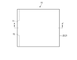
次に、調光素子11の構成について説明する。図2は、調光素子11の平面図である。図3は、図2のA−A´線に沿った調光素子11の断面図である。
[1-1] Configuration of
調光素子11の平面形状は、任意の形状とすることが可能であり、例えば四角形である。調光素子11が調光フィルムである場合、調光フィルムは、貼り付けられる領域の外形に合わせて加工される。
The planar shape of the dimming
調光素子11は、対向配置された基材20、21と、基材20、21間に配置された液晶層(調光層)24とを備える。基材20、21は、透明部材から構成され、例えば透明フィルムから構成される。基材20、21には、例えば、ポリエチレンテレフタレート(PET)フィルム、ポリエチレン(PE)フィルム、及びポリカーボネート(PC)フィルムなどを用いることができる。
The dimming
液晶層24は、液晶材料24A及び高分子材料24Bを備える。液晶層24は、高分子分散型液晶(PDLC:Polymer Dispersed Liquid Crystal)、又はポリマーネットワーク型液晶(PNLC:Polymer Network Liquid Crystal)から構成される。高分子分散型液晶は、高分子材料からなるマトリックス中に液晶材料を分散させた複合体からなり、すなわち、マトリックス中において液晶が相分離した構造を有する。ポリマーネットワーク型液晶は、高分子材料からなる3次元網目構造(ポリマーネットワーク)中に連続相を有する液晶材料を満たした複合体からなる。高分子材料としては光硬化樹脂を用いることができる。例えば、PDLCは、光重合型の高分子前駆体(モノマー)に液晶材料を混合させた溶液に紫外線を照射し、モノマーを重合させてポリマーを形成し、そのポリマーからなるマトリックス中に液晶が分散される。
The
透明電極22は、液晶層24に接するようにして、基材20上に設けられる。透明電極23は、液晶層24に接するようにして、基材21上に設けられる。透明電極22、23は、光透過性及び導電性を有する材料からなり、例えばITO(インジウム錫酸化物)から構成される。
The
調光素子11は、透明電極23に電気的に接続された端子T1と、透明電極22に電気的に接続された端子T2とを備える。端子T1、T2は、例えば、調光素子11の一側部にまとめて配置される。端子T1、T2は、駆動回路12に電気的に接続される。端子T1、T2は、金属(例えば、金、銀、銅、及びアルミニウムなど)から構成される。
The dimming
液晶層24は、シール材25によって透明電極22、23間に封止される。シール材25は、液晶層24を囲むように形成される。シール材25は、例えば光硬化樹脂から構成される。液晶層24の材料によっては、シール材25は必ずしも必要ではない。
The
[1−2] 液晶層24の動作
次に、液晶層(調光層)24の大まかな動作について説明する。
[1-2] Operation of the
液晶層24において、液晶材料の常光屈折率と高分子材料の屈折率とは概略同じに設定される。液晶材料としては、例えば、正の誘電率異方性を有するポジ型(P型)のネマティック液晶が用いられる。
In the
まず、オフ状態における液晶層24の動作について説明する。オフ状態とは、透明電極22と透明電極23とに同電圧(例えば0V)が印加された状態であり、液晶層24に電界が印加されていない状態である。図3は、オフ状態における液晶層24の様子を示している。
First, the operation of the
液晶層24に電圧(電界)が印加されない場合、液晶分子は、高分子マトリックス(又はポリマーネットワーク)の界面に対してランダムな状態になる。この場合、液晶材料の屈折率と高分子マトリックスの屈折率とが異なる状態となり、入射光は高分子マトリックスの界面で散乱する。すなわち、液晶分子が配向されていない状態において、液晶層24は高ヘイズ状態となる。このとき、液晶層24は白濁した状態となり、調光素子11は、不透明な状態となる。よって、調光素子11は、対象物を観察者から遮蔽することができる。ヘイズ値は、部材の透明性に関する指標であり、曇り度を表す。ヘイズ値が小さいほど、透明度が高い。
When no voltage (electric field) is applied to the
次に、オン状態における液晶層24の動作について説明する。オン状態とは、透明電極22と透明電極23とに異なる電圧(例えば0V及び正電圧)が印加された状態であり、液晶層24に電界が印加されている状態である。なお、透明電極22と透明電極23とには、交流電圧が印加される。図4は、オン状態における液晶層24の様子を示している。
Next, the operation of the
液晶層24に電圧が印加された場合、液晶分子の長軸(ダイレクタ)は、電極面に対して概略垂直方向に配向する。この場合、液晶材料の屈折率と高分子マトリックスの屈折率とが概略同じ状態になり、入射光は、液晶層24内でほとんど散乱されず、液晶層24を透過する。すなわち、液晶分子が配向されている状態において、液晶層24は低ヘイズ状態となる。このとき、調光素子11は、透明な状態となる。よって、観察者は、調光素子11越しに対象物を観察することができる。
When a voltage is applied to the
なお、本実施形態では、非通電時に不透明状態となり、通電時に透明状態となる調光素子について説明しているが、これに限定されるものではない。非通電時に透明状態となり、通電時に不透明状態となるリバースタイプにも適用可能である。 In this embodiment, a dimming element that becomes opaque when not energized and becomes transparent when energized is described, but the present invention is not limited to this. It can also be applied to the reverse type, which becomes transparent when not energized and opaque when energized.
[1−3] 調光素子11の等価回路
次に、調光素子11の等価回路について説明する。図5は、調光素子11の等価回路図である。
[1-3] Equivalent circuit of the dimming
透明電極22は、平面状に形成される。よって、透明電極22は、端子側(端子T1、T2が配置される側)から末端側(端子T1、T2と反対側)まで広がるように、複数の抵抗成分R1〜11を構成する。
The
同様に、透明電極23は、平面状に形成される。よって、透明電極23は、端子側から末端側まで広がるように、複数の抵抗成分R12〜22を構成する。
Similarly, the
液晶層24は、透明電極22と透明電極23との間に接続された複数の容量成分C1〜C4を構成する。
The
図4から理解できるように、調光素子11は、抵抗成分の電圧降下に起因して、端子側から末端側にいくにつれて、電圧が低くなる。すなわち、調光素子11は、端子側の電圧が高く、末端側の電圧が低くなる。末端側のノードをN1、N2と表記する。
As can be understood from FIG. 4, the voltage of the dimming
[1−4] 駆動回路12の構成
次に、駆動回路12の構成について説明する。図6は、駆動回路12を主として示した回路図である。
[1-4] Configuration of
制御回路14は、信号OVPOSIN、信号CONPOSIN、信号OVNEGIN、及び信号CONNEGINを生成し、これらの制御信号を駆動回路12に送る。信号OVPOSIN、信号CONPOSIN、信号OVNEGIN、及び信号CONNEGINの電圧波形については、後述する。
The
電源回路13は、オーバードライブ用の正側電圧源30、オーバードライブ用の負側電圧源31、液晶の配向を制御するための正側制御電圧を生成する電圧源32、及び負側制御電圧を生成する電圧源33を備える。電圧源30は、オーバードライブ電圧Vov+を生成する。電圧源31は、オーバードライブ電圧Vov−を生成する。電圧源32は、制御電圧Vc+を生成する。電圧源33は、制御電圧Vc−を生成する。“Vov+>Vc+>Vc−>Vov−”の関係を有する。
The
正側制御電圧Vc+、負側制御電圧Vc−は、最終的な液晶の配向を制御する電圧であり、使用される液晶材料に応じて決定される。すなわち、液晶材料に応じて液晶分子が垂直に配向する電圧(液晶の閾値電圧)が決定され、電圧“(Vc+)−(Vc−)”は、液晶の閾値電圧と同じか若干高く設定される。電圧“(Vov+)−(Vov−)”は、液晶の耐圧より小さく設定される。例えば、Vov+=70V、Vov−=0V、Vc+=55V、Vc−=15Vである。 The positive side control voltage Vc + and the negative side control voltage Vc− are voltages that control the final orientation of the liquid crystal, and are determined according to the liquid crystal material used. That is, the voltage at which the liquid crystal molecules are vertically oriented (the threshold voltage of the liquid crystal) is determined according to the liquid crystal material, and the voltage "(Vc +)-(Vc-)" is set to be the same as or slightly higher than the threshold voltage of the liquid crystal. .. The voltage "(Vov +)-(Vov-)" is set to be smaller than the withstand voltage of the liquid crystal display. For example, Vov + = 70V, Vov− = 0V, Vc += 55V, Vc− = 15V.
駆動回路12は、スイッチング素子40〜47を備える。スイッチング素子40の第1端子は、電圧源30に接続され、その第2端子は、端子T1に接続され、その制御端子には、信号OVPOSINが入力される。スイッチング素子40は、信号OVPOSINがハイレベル(例えば電圧Vdd=5V)の場合にオンし、信号OVPOSINがローレベル(例えば0V)の場合にオフする。
The
スイッチング素子41の第1端子は、電圧源31に接続され、その第2端子は、端子T1に接続され、その制御端子には、信号OVNEGINが入力される。スイッチング素子41は、信号OVNEGINがハイレベルの場合にオンし、信号OVNEGINがローレベルの場合にオフする。
The first terminal of the switching
スイッチング素子42の第1端子は、電圧源30に接続され、その第2端子は、端子T2に接続され、その制御端子には、信号OVNEGINが入力される。スイッチング素子42は、信号OVNEGINがハイレベルの場合にオンし、信号OVNEGINがローレベルの場合にオフする。
The first terminal of the switching
スイッチング素子43の第1端子は、電圧源31に接続され、その第2端子は、端子T2に接続され、その制御端子には、信号OVPOSINが入力される。スイッチング素子43は、信号OVPOSINがハイレベルの場合にオンし、信号OVPOSINがローレベルの場合にオフする。
The first terminal of the switching
スイッチング素子44の第1端子は、電圧源33に接続され、その第2端子は、端子T1に接続され、その制御端子には、信号CONNEGINが入力される。スイッチング素子44は、信号CONNEGINがハイレベルの場合にオンし、信号CONNEGINがローレベルの場合にオフする。
The first terminal of the switching
スイッチング素子45の第1端子は、電圧源32に接続され、その第2端子は、端子T1に接続され、その制御端子には、信号CONPOSINが入力される。スイッチング素子45は、信号CONPOSINがハイレベルの場合にオンし、信号CONPOSINがローレベルの場合にオフする。
The first terminal of the switching
スイッチング素子46の第1端子は、電圧源33に接続され、その第2端子は、端子T2に接続され、その制御端子には、信号CONPOSINが入力される。スイッチング素子46は、信号CONPOSINがハイレベルの場合にオンし、信号CONPOSINがローレベルの場合にオフする。
The first terminal of the switching
スイッチング素子47の第1端子は、電圧源32に接続され、その第2端子は、端子T2に接続され、その制御端子には、信号CONNEGINが入力される。スイッチング素子47は、信号CONNEGINがハイレベルの場合にオンし、信号CONNEGINがローレベルの場合にオフする。
The first terminal of the switching
[2] 調光装置10の動作
上記のように構成された調光装置10の動作について説明する。図7は、制御回路14の動作を説明するタイミング図である。前述したように、制御回路14は、信号OVPOSIN、信号CONPOSIN、信号OVNEGIN、及び信号CONNEGINを生成する。
[2] Operation of the dimming
時刻t0において、制御回路14は、信号OVPOSINをハイレベル(例えば電圧Vdd=5V)にする。時刻t1において、制御回路14は、信号OVPOSINをローレベル(例えば0V)にし、信号CONPOSINをハイレベルにする。
At time t0, the
時刻t2において、制御回路14は、信号CONPOSINをローレベルにし、信号OVNEGINをハイレベルにする。時刻t3において、制御回路14は、信号OVNEGINをローレベルにし、信号CONNEGINをハイレベルにする。
At time t2, the
時刻t4において、制御回路14は、信号CONNEGINをローレベルにし、信号OVPOSINをハイレベルにする。時刻t0〜t4が1つのサイクルであり、以後、同様のサイクルが繰り返される。
At time t4, the
図8は、駆動回路12の動作を説明するタイミング図である。図8の時刻t0〜t9は、図7の時刻t0〜t9に対応する。図8には、(1)駆動回路12が調光素子11の端子T1に印加する駆動電圧OUT1、(2)駆動回路12が調光素子11の端子T2に印加する駆動電圧OUT2、(3)調光素子11のノードN1の電圧V1out、及び(4)調光素子11のノードN2の電圧V2outを示している。駆動電圧OUT1が実線、駆動電圧OUT2が破線、電圧V1outが一点鎖線、電圧V2outが二点鎖線で示される。
FIG. 8 is a timing diagram illustrating the operation of the
期間t0〜t1において、スイッチング素子40がオンし、電圧OUT1=Vov+に設定される。また、期間t0〜t1において、スイッチング素子43がオンし、電圧OUT2=Vov−に設定される。これにより、末端側の電圧V1outは、端子T1に制御電圧Vc+を印加する場合に比べて、速く立ち上がる。また、末端側の電圧V2outは、端子T2に制御電圧Vc−を印加する場合に比べて、速く立ち下がる。
In the period t0 to t1, the switching
期間t1〜t2において、スイッチング素子45がオンし、電圧OUT1=Vc+に設定される。また、期間t1〜t2において、スイッチング素子46がオンし、電圧OUT2=Vc−に設定される。これにより、末端側の電圧V1outは、制御電圧Vc+に設定され、末端側の電圧V2outは、制御電圧Vc−に設定される。
In the periods t1 to t2, the switching
期間t2〜t3において、スイッチング素子41がオンし、電圧OUT1=Vov−に設定される。また、期間t2〜t3において、スイッチング素子42がオンし、電圧OUT2=Vov+に設定される。これにより、末端側の電圧V1outは、端子T1に制御電圧Vc−を印加する場合に比べて、速く立ち下がる。また、末端側の電圧V2outは、端子T2に制御電圧Vc+を印加する場合に比べて、速く立ち上がる。
In the period t2 to t3, the switching
期間t3〜t4において、スイッチング素子44がオンし、電圧OUT1=Vc−に設定される。また、期間t3〜t4において、スイッチング素子47がオンし、電圧OUT2=Vc+に設定される。これにより、末端側の電圧V1outは、制御電圧Vc−に設定され、末端側の電圧V2outは、制御電圧Vc+に設定される。
In the period t3 to t4, the switching
以後、サイクルt0〜t4と同じ動作が繰り返される。例えば、駆動周波数は、20Hzである。 After that, the same operation as in cycles t0 to t4 is repeated. For example, the drive frequency is 20 Hz.
なお、オーバードライブ期間、すなわち、期間t0〜t1、及び期間t2〜t3の各々は、調光素子11の負荷(抵抗及び容量)に応じて設定される。すなわち、オーバードライブ期間は、末端側の電圧V1outが制御電圧Vc−から制御電圧Vc+に立ち上がる期間より短く設定される。また、オーバードライブ期間は、末端側の電圧V2outが制御電圧Vc+から制御電圧Vc−に立ち下がる期間より短く設定される。
The overdrive period, that is, each of the periods t0 to t1 and the periods t2 to t3 is set according to the load (resistance and capacitance) of the dimming
図9は、調光素子11における電圧対透過率(V−T:voltage-transmittance)特性の一例を示すグラフである。図9の横軸が電圧(V)、縦軸が透過率(%)であり、図9の横軸及び縦軸ともに任意単位である。図9の電圧は、液晶層に印加される電圧、すなわち、電極22、23間の電圧である。
FIG. 9 is a graph showing an example of voltage-transmittance (VT) characteristics of the dimming
図9から理解できるように、調光素子11に印加する電圧(駆動電圧)を変化させることで、調光素子11の透過率を変化させることができる。また、調光素子11に飽和電圧以上の駆動電圧を印加しても、透過率は変わらない。飽和電圧とは、最大透過率を実現する電圧のうち最小電圧である。例えば、電圧“(Vc+)−(Vc−)”は、飽和電圧以下に設定される。よって、オーバードライブ電圧を液晶の耐圧を越えない範囲で、飽和電圧以上の電圧に設定した場合でも、オーバードライブ電圧を用いて、液晶の透過率に影響を及ぼすことなく、調光素子11を駆動できる。
As can be understood from FIG. 9, the transmittance of the dimming
端子側の実効電圧は、ほぼ制御電圧Vc+、Vc−となる。また、末端側の電圧がより速いタイミングで制御電圧Vc+、Vc−に到達するため、末端側の実効電圧も制御電圧Vc+、Vc−に近くなる。これにより、端子側と末端側との透過率の差が小さくなり、色ムラを低減することができる。 The effective voltage on the terminal side is approximately the control voltage Vc + or Vc−. Further, since the voltage on the terminal side reaches the control voltages Vc + and Vc− at a faster timing, the effective voltage on the terminal side also becomes close to the control voltages Vc + and Vc−. As a result, the difference in transmittance between the terminal side and the terminal side becomes small, and color unevenness can be reduced.
また、ゼロクロス点(電圧V1outと電圧V2outとが交差する点)を含む極性反転を行う期間(例えば、図8の期間t0〜t1)では、液晶に印加される実効電圧が低いため、液晶の透過率は、所望の透過率にならない。特に、ゼロクロス点では、液晶に印加される電圧は、0Vである。しかし、本実施形態では、オーバードライブ駆動を用いることで、末端側の電圧がより速いタイミングで上昇する。これにより、極性反転を行う期間を短くできるので、フリッカーを低減することができる。 Further, in the period during which the polarity is reversed including the zero cross point (the point where the voltage V1out and the voltage V2out intersect) (for example, the period t0 to t1 in FIG. 8), the effective voltage applied to the liquid crystal is low, so that the liquid crystal is transmitted. The rate does not reach the desired transmittance. In particular, at the zero cross point, the voltage applied to the liquid crystal is 0V. However, in the present embodiment, by using the overdrive drive, the voltage on the terminal side rises at a faster timing. As a result, the period for performing polarity reversal can be shortened, so that flicker can be reduced.
[3] 比較例
次に、比較例に係る調光装置について説明する。図10は、比較例に係る駆動回路の回路図である。
[3] Comparative Example Next, the dimming device according to the comparative example will be described. FIG. 10 is a circuit diagram of a drive circuit according to a comparative example.
電圧源32は、制御電圧Vc+を生成する。電圧源33は、制御電圧Vc−を生成する。例えば、Vc+=40V、Vc−=0Vである。
The
スイッチング素子44の第1端子は、電圧源33に接続され、その第2端子は、端子T1に接続され、その制御端子には、信号NEGINが入力される。スイッチング素子44は、信号NEGINがハイレベルの場合にオンし、信号NEGINがローレベルの場合にオフする。
The first terminal of the switching
スイッチング素子45の第1端子は、電圧源32に接続され、その第2端子は、端子T1に接続され、その制御端子には、信号POSINが入力される。スイッチング素子45は、信号POSINがハイレベルの場合にオンし、信号POSINがローレベルの場合にオフする。
The first terminal of the switching
スイッチング素子46の第1端子は、電圧源33に接続され、その第2端子は、端子T2に接続され、その制御端子には、信号POSINが入力される。スイッチング素子46は、信号POSINがハイレベルの場合にオンし、信号POSINがローレベルの場合にオフする。
The first terminal of the switching
スイッチング素子47の第1端子は、電圧源32に接続され、その第2端子は、端子T2に接続され、その制御端子には、信号NEGINが入力される。スイッチング素子47は、信号NEGINがハイレベルの場合にオンし、信号NEGINがローレベルの場合にオフする。
The first terminal of the switching
図11は、比較例に係る調光装置の動作を説明する図である。時刻t0において、信号POSINがハイレベルにされ、信号NEGINがローレベルにされる。時刻t1において、信号POSINがローレベルにされ、信号NEGINがハイレベルにされる。時刻t2において、信号POSINがハイレベルにされ、信号NEGINがローレベルにされる。 FIG. 11 is a diagram illustrating the operation of the dimming device according to the comparative example. At time t0, the signal POSIN is set to high level and the signal NEGIN is set to low level. At time t1, the signal POSIN is set to low level and the signal NEGIN is set to high level. At time t2, the signal POSIN is set to a high level and the signal NEGIN is set to a low level.
期間t0〜t1において、スイッチング素子45がオンし、電圧OUT1=Vc+に設定される。また、期間t0〜t1において、スイッチング素子46がオンし、電圧OUT2=Vc−に設定される。これにより、末端側の電圧V1outは、オーバードライブ駆動に比べて、緩やかに立ち上がる。また、末端側の電圧V2outは、オーバードライブ駆動に比べて、緩やかに立ち下がる。
In the period t0 to t1, the switching
期間t1〜t2において、スイッチング素子44がオンし、電圧OUT1=Vc−に設定される。また、期間t1〜t2において、スイッチング素子47がオンし、電圧OUT2=Vc+に設定される。これにより、末端側の電圧V1outは、オーバードライブ駆動に比べて、緩やかに立ち下がる。また、末端側の電圧V2outは、オーバードライブ駆動に比べて、緩やかに立ち上がる。
In the periods t1 to t2, the switching
比較例では、極性反転において、末端側の電圧V1out、電圧V2outが所望の電圧(Vc+、Vc−)になるまでの時間が長い。これにより、比較例では、フリッカーが大きくなってしまう。また、比較例では、端子側と末端側とで実効電圧が異なる期間が長くなるため、色ムラが発生してしまう。 In the comparative example, in the polarity inversion, it takes a long time for the voltage V1out and the voltage V2out on the terminal side to reach the desired voltage (Vc +, Vc−). As a result, in the comparative example, the flicker becomes large. Further, in the comparative example, since the period in which the effective voltage differs between the terminal side and the terminal side becomes long, color unevenness occurs.
[4] 第1実施形態の効果
以上詳述したように第1実施形態では、調光装置10は、対向配置された基材20、21と、基材20、21にそれぞれ設けられた透明電極22、23と、透明電極22、23間に充填された液晶層24と、透明電極22、23に電気的に接続された端子T1、T2とを含む調光素子11と、端子T1に駆動電圧OUT1を印加し、端子T2に駆動電圧OUT1と極性が異なる駆動電圧OUT2を印加する駆動回路12とを具備する。駆動電圧OUT1は、第1期間において正側オーバードライブ電圧Vov+に設定され、前記第1期間に続く第2期間において正側制御電圧Vc+に設定され、第2期間に続く第3期間において負側オーバードライブ電圧Vov−に設定され、第3期間に続く第4期間において負側制御電圧Vc−に設定される。
[4] Effect of First Embodiment As described in detail above, in the first embodiment, the dimming
従って第1実施形態によれば、端子側と反対側の電圧を、より速く制御電圧Vc+、Vc−に設定することができる。これにより、端子側と末端側との透過率の差が小さくなり、色ムラを低減することができる。 Therefore, according to the first embodiment, the voltage on the side opposite to the terminal side can be set to the control voltages Vc + and Vc− faster. As a result, the difference in transmittance between the terminal side and the terminal side becomes small, and color unevenness can be reduced.
また、ゼロクロス点(電圧V1outと電圧V2outとが交差する点)を含む極性反転を行う期間では、フリッカーが発生する原因となる。しかし、本実施形態では、極性反転を行う期間を短くできるので、フリッカーを低減することができる。 Further, in the period of performing polarity reversal including the zero cross point (the point where the voltage V1out and the voltage V2out intersect), flicker occurs. However, in the present embodiment, the period for performing polarity reversal can be shortened, so that flicker can be reduced.
図12は、第1例に係る消費される電荷量の模式図である。図12の横軸は、端子−末端間の位置を表し、縦軸は、液晶に印加される電圧(印加電圧)を表している。例えば、0V〜40Vの領域は、透過率を変化させることが可能な階調領域であり、40V〜70Vの領域は、透過率がほぼ変化しない飽和領域である。 FIG. 12 is a schematic diagram of the amount of electric charge consumed according to the first example. The horizontal axis of FIG. 12 represents the position between the terminal and the end, and the vertical axis represents the voltage (applied voltage) applied to the liquid crystal display. For example, the region of 0V to 40V is a gradation region in which the transmittance can be changed, and the region of 40V to 70V is a saturation region in which the transmittance hardly changes.
電荷量Aは、通常パルス駆動における電荷量である。第1例の通常パルス駆動は、印加電圧40Vを用い、かつ末端側の電圧が40Vになるまで周波数を低くして駆動する例である。通常パルス駆動では、末端側が最終的に40Vになるので、端子側と末端側との色ムラは低減できる。しかし、極性反転にかかる時間が長くなるので、フリッカーが大きくなる。 The amount of charge A is the amount of charge in a normal pulse drive. The normal pulse drive of the first example is an example in which an applied voltage of 40 V is used and the frequency is lowered until the voltage on the terminal side becomes 40 V. In the normal pulse drive, the terminal side finally becomes 40 V, so that the color unevenness between the terminal side and the terminal side can be reduced. However, since the time required for polarity reversal becomes long, flicker becomes large.
電荷量Bは、通常パルス駆動に対するオーバードライブ駆動で増加する電荷量である。オーバードライブ駆動は、オーバードライブ電圧70Vを用いて駆動する例である。端子側から末端側にいくにつれて電圧が低くなるので、電荷量Bは、端子側から末端側に向かって漸減する三角形で表される。オーバードライブ駆動を行う場合、電荷量Bの増加のみで、通常パルス駆動に比べて、フリッカーを低減できるとともに、色ムラが低減できる。 The charge amount B is a charge amount that increases due to overdrive drive with respect to normal pulse drive. The overdrive drive is an example of driving using an overdrive voltage of 70V. Since the voltage decreases from the terminal side to the terminal side, the charge amount B is represented by a triangle that gradually decreases from the terminal side to the terminal side. When the overdrive drive is performed, flicker can be reduced and color unevenness can be reduced as compared with the normal pulse drive only by increasing the charge amount B.
電荷量Cは、フル駆動に対するオーバードライブ駆動で減少する電荷量である。フル駆動は、70Vを用いて駆動する例である。すなわち、“電荷量A+電荷量B+電荷量C”がフル駆動の電荷量である。フル駆動では、フリッカーは低減されるが、消費される電荷量が大きくなる。オーバードライブ駆動では、フル駆動と同程度にフリッカーを低減できつつ、フル駆動に比べて消費される電荷量を低減できる。 The electric charge amount C is an electric charge amount that is reduced by the overdrive drive with respect to the full drive. Full drive is an example of driving using 70V. That is, "charge amount A + charge amount B + charge amount C" is the full drive charge amount. At full drive, flicker is reduced, but the amount of charge consumed is higher. In the overdrive drive, flicker can be reduced to the same extent as in the full drive, and the amount of charge consumed can be reduced as compared with the full drive.
図13は、第2例に係る消費される電荷量の模式図である。第2例は、中間調を実施した場合の例である。 FIG. 13 is a schematic diagram of the amount of electric charge consumed according to the second example. The second example is an example in which a halftone is performed.
電荷量Dは、通常パルス駆動における電荷量である。第2例の通常パルス駆動は、印加電圧20Vを用い、かつ末端側の電圧が20Vになるまで周波数を低くして駆動する例である。通常パルス駆動では、末端側が最終的に20Vになるので、端子側と末端側との色ムラは低減できる。しかし、極性反転にかかる時間が長くなるので、フリッカーが大きくなる。また、フリッカーを低減させるために、周波数を大きくすると、端子側と末端側との電位差が大きくなり、色ムラが発生する。周波数を大きくした場合の電荷量は、図13の破線で示した下の領域である。すなわち、色ムラとフリッカーとはトレードオフの関係にある。 The amount of charge D is the amount of charge in a normal pulse drive. The normal pulse drive of the second example is an example in which an applied voltage of 20 V is used and the frequency is lowered until the voltage on the terminal side becomes 20 V. In the normal pulse drive, the terminal side finally becomes 20 V, so that the color unevenness between the terminal side and the terminal side can be reduced. However, since the time required for polarity reversal becomes long, flicker becomes large. Further, when the frequency is increased in order to reduce flicker, the potential difference between the terminal side and the terminal side becomes large, and color unevenness occurs. The amount of charge when the frequency is increased is the lower region shown by the broken line in FIG. That is, there is a trade-off relationship between color unevenness and flicker.
電荷量Eは、通常パルス駆動に対するオーバードライブ駆動で増加する電荷量である。オーバードライブ駆動を用いて中間調を実施した場合でも、電荷量Eの増加のみで、通常パルス駆動に比べて、フリッカーを低減できるとともに、色ムラが低減できる。また、第2例の場合も、オーバードライブ駆動では、70Vのフル駆動と同程度にフリッカーを低減できる。 The charge amount E is a charge amount that increases due to overdrive drive with respect to normal pulse drive. Even when the halftone is performed by using the overdrive drive, the flicker can be reduced and the color unevenness can be reduced as compared with the normal pulse drive only by increasing the charge amount E. Further, also in the case of the second example, in the overdrive drive, flicker can be reduced to the same extent as in the full drive of 70V.
[第2実施形態]
第2実施形態は、駆動回路12、及び電源回路13の具体的な構成例である。第2実施形態は、トランジスタを用いてデジタル式に駆動回路12を構成した例である。
[Second Embodiment]
The second embodiment is a specific configuration example of the
図14は、本発明の第2実施形態に係る駆動回路12を主として示した回路図である。本実施形態では、駆動回路12を構成する複数のスイッチング素子の各々は、MOSトランジスタ、又はバイポーラトランジスタから構成される。本実施形態では、NチャネルMOSトランジスタ(又はパワーMOSトランジスタ)を用いる例について説明する。調光素子11は、等価回路として表現すると、図5から理解されるように、抵抗性負荷RLと、容量性負荷CLとを含む。
FIG. 14 is a circuit diagram mainly showing the
駆動回路12は、ゲートドライバ12Aを備える。ゲートドライバ12Aは、前述した信号OVPOSIN、信号CONPOSIN、信号OVNEGIN、及び信号CONNEGINを出力する。ゲートドライバ12Aは、信号OVPOSIN、信号CONPOSIN、信号OVNEGIN、及び信号CONNEGINを、トランジスタに最適なゲート電圧レベルに設定する。制御回路14は、タイミング発生回路14Aを備える。タイミング発生回路14Aは、信号OVPOSIN、信号CONPOSIN、信号OVNEGIN、及び信号CONNEGINのタイミングを制御する。
The
駆動回路12は、NチャネルMOSトランジスタ40〜43、44A、44B、45A、45B、46A、46B、47A、47Bを備える。
The
トランジスタ40のドレインは、オーバードライブ電圧Vov+を生成する電圧源30に接続され、そのソースは、端子T1に接続され、そのゲートには、信号OVPOSINが入力される。
The drain of the
トランジスタ41のドレインは、端子T1に接続され、そのソースは、オーバードライブ電圧Vov−を生成する電圧源31に接続され、そのゲートには、信号OVNEGINが入力される。
The drain of the
トランジスタ42のドレインは、電圧源30に接続され、そのソースは、端子T2に接続され、そのゲートには、信号OVNEGINが入力される。
The drain of the
トランジスタ43のドレインは、端子T2に接続され、そのソースは、電圧源31に接続され、そのゲートには、信号OVPOSINが入力される。
The drain of the
トランジスタ44A、44Bは、図6のスイッチング素子44を構成する。トランジスタ44Aのドレインは、端子T1に接続され、そのソースは、トランジスタ44Bのソースに接続され、そのゲートには、信号CONNEGINが入力される。トランジスタ44Bのドレインは、制御電圧Vc−を生成する電圧源33に接続され、そのゲートには、信号CONNEGINが入力される。
The
トランジスタ45A、45Bは、図6のスイッチング素子45を構成する。トランジスタ45Aのドレインは、端子T1に接続され、そのソースは、トランジスタ45Bのソースに接続され、そのゲートには、信号CONPOSINが入力される。トランジスタ45Bのドレインは、制御電圧Vc+を生成する電圧源32に接続され、そのゲートには、信号CONPOSINが入力される。
The
トランジスタ46A、46Bは、図6のスイッチング素子46を構成する。トランジスタ46Aのドレインは、端子T2に接続され、そのソースは、トランジスタ46Bのソースに接続され、そのゲートには、信号CONPOSINが入力される。トランジスタ46Bのドレインは、電圧源33に接続され、そのゲートには、信号CONPOSINが入力される。
The
トランジスタ47A、47Bは、図6のスイッチング素子47を構成する。トランジスタ47Aのドレインは、端子T2に接続され、そのソースは、トランジスタ47Bのソースに接続され、そのゲートには、信号CONNEGINが入力される。トランジスタ47Bのドレインは、電圧源32に接続され、そのゲートには、信号CONNEGINが入力される。
The
電源回路13は、電圧源13A、及び電圧源30〜33を備える。電圧源13Aは、電源電圧VCCから電圧Vinを生成する。
The
電圧源30は、定電圧素子としてのツェナーダイオード(定電圧ダイオード)30A、及び抵抗30Bを備える。ツェナーダイオード30Aのカソードは、電圧源13Aに接続され、そのアノードは、抵抗30Bの一端に接続される。抵抗30Bの他端は、接地端子GNDに接続される。電圧源30は、他の構成を用いてもよい。例えば、扱う電圧が大きい場合には、2個又はそれ以上のツェナーダイオードを直列接続してもよい。また、ツェナーダイオード30Aと抵抗30Bとの接続ノードに、電流増幅用のNPNトランジスタを追加してもよい。また、電圧源30は、電圧制御端子を備えたシリーズレギュレータで構成してもよい。また、電圧源30は、DC/DCコンバータで構成してもよい。
The
電圧源32は、ツェナーダイオード32A、及び抵抗32Bを備える。抵抗32Bの一端は、電圧源13Aに接続され、その他端は、ツェナーダイオード32Aのカソードに接続される。ツェナーダイオード32Aのアノードは、接地端子GNDに接続される。電圧源32には、電圧源30と同様の他の構成例を用いてもよい。
The
電圧源33は、ツェナーダイオード33A、及び抵抗33Bを備える。ツェナーダイオード33Aのカソードは、電圧源13Aに接続され、そのアノードは、抵抗33Bの一端に接続される。抵抗33Bの他端は、接地端子GNDに接続される。電圧源33には、電圧源30と同様の他の構成例を用いてもよい。
The
以上詳述したように第2実施形態では、トランジスタを用いて駆動回路12を構成することができる。第2実施形態の電圧制御は、第1実施形態の電圧制御と同じである。その他の効果は、第1実施形態と同じである。
As described in detail above, in the second embodiment, the
[第3実施形態]
第3実施形態は、駆動回路12、及び電源回路13の具体的な構成例である。第3実施形態は、電力増幅器を用いてアナログ式に駆動回路12を構成した例である。
[Third Embodiment]
The third embodiment is a specific configuration example of the
図15は、本発明の第3実施形態に係る駆動回路12を主として示した回路図である。駆動回路12は、オーバードライブ波形発生回路12B、及び電力増幅器12C、12Dを備える。オーバードライブ波形発生回路12Bは、タイミング発生回路14Aからの制御信号を用いて、正側電圧波形VP、及び負側電圧波形VNを生成する。
FIG. 15 is a circuit diagram mainly showing the
電力増幅器12C、12Dは、第1象限から第4象限までの動作が可能な4象限出力が可能である。すなわち、電力増幅器12C、12Dは、電圧の向きによらず、電流の供給(ソース)と吸収(シンク)とが可能である。
The
電力増幅器12Cは、オーバードライブ波形発生回路12Bから正極電圧波形VPを受け、この正極電圧波形VPを増幅する。電力増幅器12Cは、駆動電圧OUT1を出力する。駆動電圧OUT1は、調光素子11の端子T1に印加される。
The
電力増幅器12Dは、オーバードライブ波形発生回路12Bから負極電圧波形VNを受け、この負極電圧波形VNを増幅する。電力増幅器12Dは、駆動電圧OUT2を出力する。駆動電圧OUT2は、調光素子11の端子T2に印加される。
The
図16は、駆動回路12の動作を説明するタイミング図である。駆動電圧OUT1、OUT2は、第1実施形態の図8と同じ波形である。駆動電圧OUT1は、前段の正極電圧波形VPと波形は同じで、出力電流を増幅したものである。駆動電圧OUT2は、前段の負極電圧波形VNと波形は同じで、出力電流を増幅したものである。
FIG. 16 is a timing diagram illustrating the operation of the
第2実施形態によれば、アナログ式にオーバードライブ駆動を実現できる。その他の効果は、第1実施形態と同じである。 According to the second embodiment, the analog overdrive drive can be realized. Other effects are the same as in the first embodiment.
[実施例]
上記実施形態では、PDLC又はPNLCを用いた液晶素子(調光素子)を例示しているが、これに限定されるものではない。調光素子としての液晶素子は、偏光板及び配向膜を液晶層の両側に配置した構成でもよく、TN(Twisted Nematic)方式、VA(Vertical Alignment)方式、又はIPS(In-Plane Switching)方式などを用いることができる。また、調光素子として、液晶素子以外で、電圧により屈折率が変化する様々な種類の電気光学素子を用いることができる。
[Example]
In the above embodiment, a liquid crystal element (dimming element) using PDLC or PNLC is exemplified, but the present invention is not limited thereto. The liquid crystal element as a dimming element may be configured such that a polarizing plate and an alignment film are arranged on both sides of the liquid crystal layer, such as a TN (Twisted Nematic) method, a VA (Vertical Alignment) method, or an IPS (In-Plane Switching) method. Can be used. Further, as the dimming element, various types of electro-optical elements whose refractive index changes depending on the voltage can be used other than the liquid crystal element.
上記実施形態で示したスイッチング素子は、MOSトランジスタ、又はバイポーラトランジスタ以外に、炭化シリコン(SiC)を半導体層に用いたSiC−MOSFET、又は窒化ガリウム(GaN)を半導体層に用いたGaN−MOSFETなどで構成してもよい。 In addition to the MOS transistor or bipolar transistor, the switching element shown in the above embodiment includes a SiC- MOSFET in which silicon carbide (SiC) is used in the semiconductor layer, a GaN- MOSFET in which gallium nitride (GaN) is used in the semiconductor layer, and the like. It may be configured with.
上記実施形態で説明した調光装置は、住宅、オフィス、又は公共施設における窓や室内パーテーション、商業施設又はイベント会場における映像投影スクリーンやサイネージ、自動車又は航空機における窓やサンルーフなどに適用可能である。 The dimming device described in the above embodiment can be applied to windows and indoor partitions in houses, offices, or public facilities, image projection screens and signage in commercial facilities or event venues, windows and sunroofs in automobiles or aircraft, and the like.
上記実施形態では、液晶素子として調光素子を例に挙げて説明しているが、これに限定されず、本実施形態における駆動方法は、液晶を用いた様々な装置(液晶表示装置を含む)に適用可能である。 In the above embodiment, the dimming element is described as an example as the liquid crystal element, but the present invention is not limited to this, and the driving method in the present embodiment is various devices using a liquid crystal display (including a liquid crystal display device). Applicable to.
なお、本発明は、上記実施形態に限定されるものではなく、実施段階ではその要旨を逸脱しない範囲で種々に変形することが可能である。また、各実施形態は適宜組み合わせて実施してもよく、その場合組み合わせた効果が得られる。更に、上記実施形態には種々の発明が含まれており、開示される複数の構成要件から選択された組み合わせにより種々の発明が抽出され得る。例えば、実施形態に示される全構成要件からいくつかの構成要件が削除されても、課題が解決でき、効果が得られる場合には、この構成要件が削除された構成が発明として抽出され得る。 The present invention is not limited to the above embodiment, and can be variously modified at the implementation stage without departing from the gist thereof. In addition, each embodiment may be carried out in combination as appropriate, in which case the combined effect can be obtained. Further, the above-described embodiment includes various inventions, and various inventions can be extracted by a combination selected from a plurality of disclosed constituent requirements. For example, even if some constituent elements are deleted from all the constituent elements shown in the embodiment, if the problem can be solved and the effect is obtained, the configuration in which the constituent elements are deleted can be extracted as an invention.
10…調光装置、11…調光素子、12…駆動回路、13…電源回路、14…制御回路、20,21…基材、22,23…透明電極、24…液晶層、25…シール材、30〜33…電圧源、40〜47…スイッチング素子 10 ... dimming device, 11 ... dimming element, 12 ... drive circuit, 13 ... power supply circuit, 14 ... control circuit, 20, 21 ... base material, 22, 23 ... transparent electrode, 24 ... liquid crystal layer, 25 ... sealing material , 30-33 ... Voltage source, 40-47 ... Switching element
Claims (8)
前記第1端子に第1駆動電圧を印加し、前記第2端子に前記第1駆動電圧と極性が異なる第2駆動電圧を印加する駆動回路と
を具備し、
前記第1駆動電圧は、第1期間において第1電圧に設定され、前記第1期間に続く第2期間において前記第1電圧より低い第2電圧に設定され、前記第2期間に続く第3期間において前記第2電圧より低い第3電圧に設定され、前記第3期間に続く第4期間において前記第2電圧より低くかつ前記第3電圧より高い第4電圧に設定され、
前記第2駆動電圧は、前記第1期間において前記第3電圧に設定され、前記第2期間において前記第4電圧に設定され、前記第3期間において前記第1電圧に設定され、前記第4期間において前記第2電圧に設定され、
前記第1電圧と前記第3電圧との電圧差は、前記調光素子の耐圧より小さい
調光装置。 The first and second substrates, the first electrode provided in a plane on the first substrate, the second electrode provided in a plane on the second substrate, and the first and first electrodes. A dimming element including a polymer-dispersed or polymer network-type liquid crystal layer filled between two electrodes and first and second terminals electrically connected to the first and second electrodes.
A drive circuit for applying a first drive voltage to the first terminal and applying a second drive voltage having a polarity different from that of the first drive voltage is provided for the second terminal.
The first drive voltage is set to the first voltage in the first period, set to a second voltage lower than the first voltage in the second period following the first period, and the third period following the second period. Is set to a third voltage lower than the second voltage, and is set to a fourth voltage lower than the second voltage and higher than the third voltage in the fourth period following the third period .
The second drive voltage is set to the third voltage in the first period, set to the fourth voltage in the second period, set to the first voltage in the third period, and is set to the first voltage in the third period. Is set to the second voltage in
A dimming device in which the voltage difference between the first voltage and the third voltage is smaller than the withstand voltage of the dimming element.
請求項1に記載の調光装置。 The dimming device according to claim 1, wherein the voltage difference between the second voltage and the fourth voltage is equal to or less than the saturation voltage of the dimming element.
請求項1又は2に記載の調光装置。 The dimming device according to claim 1 or 2.
前記第3期間は、前記末端側の電圧が前記第2電圧から前記第4電圧に立ち下がる期間より短く設定される The third period is set shorter than the period during which the voltage on the terminal side drops from the second voltage to the fourth voltage.
請求項1乃至3のいずれかに記載の調光装置。 The dimming device according to any one of claims 1 to 3.
前記第1スイッチング素子は、前記第1電圧を発生する第1電圧源と前記第1端子との間に接続され、
前記第2スイッチング素子は、前記第3電圧を発生する第3電圧源と前記第1端子との間に接続され、
前記第3スイッチング素子は、前記第1電圧源と前記第2端子との間に接続され、
前記第4スイッチング素子は、前記第3電圧源と前記第2端子との間に接続され、
前記第5スイッチング素子は、前記第2電圧を発生する第2電圧源と前記第1端子との間に接続され、
前記第6スイッチング素子は、前記第4電圧を発生する第4電圧源と前記第1端子との間に接続され、
前記第7スイッチング素子は、前記第2電圧源と前記第2端子との間に接続され、
前記第8スイッチング素子は、前記第4電圧源と前記第2端子との間に接続される
請求項1乃至4のいずれかに記載の調光装置。 The drive circuit includes first to eighth switching elements.
The first switching element is connected between the first voltage source that generates the first voltage and the first terminal.
The second switching element is connected between the third voltage source that generates the third voltage and the first terminal.
The third switching element is connected between the first voltage source and the second terminal.
The fourth switching element is connected between the third voltage source and the second terminal.
The fifth switching element is connected between the second voltage source that generates the second voltage and the first terminal.
The sixth switching element is connected between the fourth voltage source that generates the fourth voltage and the first terminal.
The seventh switching element is connected between the second voltage source and the second terminal.
The dimming device according to any one of claims 1 to 4 , wherein the eighth switching element is connected between the fourth voltage source and the second terminal.
前記第1制御信号は、前記第1及び第4スイッチング素子に入力され、
前記第2制御信号は、前記第2及び第3スイッチング素子に入力され、
前記第3制御信号は、前記第5及び第8スイッチング素子に入力され、
前記第4制御信号は、前記第6及び第7スイッチング素子に入力される
請求項5に記載の調光装置。 Further provided with a control circuit for generating first to fourth control signals,
The first control signal is input to the first and fourth switching elements, and is input to the first and fourth switching elements.
The second control signal is input to the second and third switching elements, and is input to the second and third switching elements.
The third control signal is input to the fifth and eighth switching elements, and is input to the fifth and eighth switching elements.
The dimming device according to claim 5 , wherein the fourth control signal is input to the sixth and seventh switching elements.
請求項5又は6に記載の調光装置。 The dimming device according to claim 5 or 6 , wherein each of the first to fourth voltage sources includes a constant voltage element.
請求項5乃至7のいずれかに記載の調光装置。 The dimming device according to any one of claims 5 to 7 , wherein each of the first to eighth switching elements is composed of a transistor.
Priority Applications (6)
| Application Number | Priority Date | Filing Date | Title |
|---|---|---|---|
| JP2017113443A JP6981052B2 (en) | 2017-06-08 | 2017-06-08 | Dimmer |
| PCT/JP2018/021054 WO2018225625A1 (en) | 2017-06-08 | 2018-05-31 | Light control device |
| EP18812822.7A EP3637176B1 (en) | 2017-06-08 | 2018-05-31 | Light control device |
| CN201880035752.8A CN110678805B (en) | 2017-06-08 | 2018-05-31 | Light modulation device |
| US16/704,526 US10871668B2 (en) | 2017-06-08 | 2019-12-05 | Light control device |
| JP2021187781A JP7226510B2 (en) | 2017-06-08 | 2021-11-18 | dimmer |
Applications Claiming Priority (1)
| Application Number | Priority Date | Filing Date | Title |
|---|---|---|---|
| JP2017113443A JP6981052B2 (en) | 2017-06-08 | 2017-06-08 | Dimmer |
Related Child Applications (1)
| Application Number | Title | Priority Date | Filing Date |
|---|---|---|---|
| JP2021187781A Division JP7226510B2 (en) | 2017-06-08 | 2021-11-18 | dimmer |
Publications (3)
| Publication Number | Publication Date |
|---|---|
| JP2018205631A JP2018205631A (en) | 2018-12-27 |
| JP2018205631A5 JP2018205631A5 (en) | 2020-08-13 |
| JP6981052B2 true JP6981052B2 (en) | 2021-12-15 |
Family
ID=64565864
Family Applications (1)
| Application Number | Title | Priority Date | Filing Date |
|---|---|---|---|
| JP2017113443A Active JP6981052B2 (en) | 2017-06-08 | 2017-06-08 | Dimmer |
Country Status (5)
| Country | Link |
|---|---|
| US (1) | US10871668B2 (en) |
| EP (1) | EP3637176B1 (en) |
| JP (1) | JP6981052B2 (en) |
| CN (1) | CN110678805B (en) |
| WO (1) | WO2018225625A1 (en) |
Families Citing this family (3)
| Publication number | Priority date | Publication date | Assignee | Title |
|---|---|---|---|---|
| KR102018352B1 (en) * | 2019-02-25 | 2019-10-21 | 주식회사 제이앤에스 | A smart film device with improved specificity haze |
| JP7263938B2 (en) * | 2019-06-20 | 2023-04-25 | 凸版印刷株式会社 | Light control sheet driving device, light control device, light control sheet driving method, and light control sheet driving program |
| WO2022270298A1 (en) * | 2021-06-23 | 2022-12-29 | 株式会社ジャパンディスプレイ | Optical device |
Family Cites Families (15)
| Publication number | Priority date | Publication date | Assignee | Title |
|---|---|---|---|---|
| JPS6449924A (en) | 1987-08-20 | 1989-02-27 | Teraoka Seiko Kk | Strain gage type load cell |
| JPS6449924U (en) * | 1987-09-24 | 1989-03-28 | ||
| JPH10197849A (en) * | 1997-01-06 | 1998-07-31 | Matsushita Electric Ind Co Ltd | Method and device for driving antiferoelectric liquid crystal element |
| TWI259992B (en) * | 2003-05-22 | 2006-08-11 | Au Optronics Corp | Liquid crystal display device driver and method thereof |
| JP2005010202A (en) * | 2003-06-16 | 2005-01-13 | Nec Corp | Liquid crystal panel, liquid crystal display device using liquid crystal panel, and electronic device on which liquid crystal display is mounted |
| TWI329214B (en) * | 2003-12-18 | 2010-08-21 | Sharp Kk | Display element and display device, driving method of display element, and program |
| WO2006030388A2 (en) * | 2004-09-15 | 2006-03-23 | Koninklijke Philips Electronics N.V. | Display devices and methods of driving such |
| TWI282544B (en) * | 2005-01-21 | 2007-06-11 | Himax Tech Inc | Operation apparatus, operation method, operation apparatus for overdrive and operation method for overdrive |
| JP4661406B2 (en) * | 2005-07-05 | 2011-03-30 | 富士ゼロックス株式会社 | Liquid crystal device driving method and liquid crystal device driving apparatus |
| JP2007304561A (en) * | 2006-03-23 | 2007-11-22 | Toshiba Matsushita Display Technology Co Ltd | Driving device of liquid crystal display device |
| JP4645632B2 (en) * | 2007-09-21 | 2011-03-09 | ソニー株式会社 | Liquid crystal display device, driving method of liquid crystal display device, and electronic apparatus |
| US8665255B2 (en) * | 2007-11-13 | 2014-03-04 | Sharp Kabushiki Kaisha | Power supply circuit and display device including the same |
| JP2013072895A (en) * | 2011-09-26 | 2013-04-22 | Seiko Electric Co Ltd | Liquid crystal dimmer and driving device for liquid crystal dimming element |
| TWM494455U (en) * | 2014-09-23 | 2015-01-21 | Unity Opto Technology Co Ltd | Drive circuit for reducing LED flicker |
| CN110431478B (en) * | 2017-03-29 | 2022-07-05 | 默克专利股份有限公司 | Method of electrically driving a switchable optical element |
-
2017
- 2017-06-08 JP JP2017113443A patent/JP6981052B2/en active Active
-
2018
- 2018-05-31 EP EP18812822.7A patent/EP3637176B1/en active Active
- 2018-05-31 CN CN201880035752.8A patent/CN110678805B/en active Active
- 2018-05-31 WO PCT/JP2018/021054 patent/WO2018225625A1/en unknown
-
2019
- 2019-12-05 US US16/704,526 patent/US10871668B2/en active Active
Also Published As
| Publication number | Publication date |
|---|---|
| CN110678805A (en) | 2020-01-10 |
| EP3637176A4 (en) | 2020-06-10 |
| EP3637176A1 (en) | 2020-04-15 |
| EP3637176B1 (en) | 2024-04-24 |
| JP2018205631A (en) | 2018-12-27 |
| CN110678805B (en) | 2022-08-23 |
| WO2018225625A1 (en) | 2018-12-13 |
| US10871668B2 (en) | 2020-12-22 |
| US20200110297A1 (en) | 2020-04-09 |
Similar Documents
| Publication | Publication Date | Title |
|---|---|---|
| JP6733747B2 (en) | Dimmer | |
| US10871668B2 (en) | Light control device | |
| JP5188362B2 (en) | Light source driving apparatus and method for backlight unit | |
| KR20120110387A (en) | Pixel circuit and driving method of the same | |
| TW202145191A (en) | Pixel circuit and display device using pulse width modulator generator | |
| CN110428785A (en) | TFT panel control circuit | |
| KR20100006320A (en) | Apparatus and method for driving light source in back light unit | |
| CN102930841A (en) | Pixel circuit of smectic state liquid crystal multistable electronic paper display | |
| US10971106B2 (en) | Liquid crystal optical modulation device and liquid crystal optical modulation method | |
| WO2018186447A1 (en) | Liquid crystal dimming device and liquid crystal dimming method | |
| JP6836010B2 (en) | DC voltage conversion circuit, DC voltage conversion method, and liquid crystal display | |
| JP7226510B2 (en) | dimmer | |
| US20090073156A1 (en) | Drive Circuits for Capacitive Loads | |
| RU2653769C1 (en) | Liquid crystal 3d panel with "naked eye" technology and the panel control method | |
| KR101510885B1 (en) | Apparatus and Method for Driving Light Source in Back Light Unit | |
| KR20000006515A (en) | Method for driving a liquid crystal display | |
| CN201765805U (en) | Current control circuit | |
| JP3587101B2 (en) | Power supply circuit and electro-optical device | |
| KR100265782B1 (en) | Liquid crystal display apparatus of a thin-film transistor type | |
| TWI537929B (en) | Liquid crystal display device and driving control circuit thereof | |
| KR102029851B1 (en) | Light driving apparatus and aliquid crystal display device having the same | |
| KR20070071338A (en) | Inverter driving method for plat panel display |
Legal Events
| Date | Code | Title | Description |
|---|---|---|---|
| A711 | Notification of change in applicant |
Free format text: JAPANESE INTERMEDIATE CODE: A712 Effective date: 20190425 |
|
| A621 | Written request for application examination |
Free format text: JAPANESE INTERMEDIATE CODE: A621 Effective date: 20200518 |
|
| A521 | Request for written amendment filed |
Free format text: JAPANESE INTERMEDIATE CODE: A523 Effective date: 20200630 |
|
| A131 | Notification of reasons for refusal |
Free format text: JAPANESE INTERMEDIATE CODE: A131 Effective date: 20210622 |
|
| A521 | Request for written amendment filed |
Free format text: JAPANESE INTERMEDIATE CODE: A523 Effective date: 20210812 |
|
| TRDD | Decision of grant or rejection written | ||
| A01 | Written decision to grant a patent or to grant a registration (utility model) |
Free format text: JAPANESE INTERMEDIATE CODE: A01 Effective date: 20211019 |
|
| A61 | First payment of annual fees (during grant procedure) |
Free format text: JAPANESE INTERMEDIATE CODE: A61 Effective date: 20211101 |
|
| R150 | Certificate of patent or registration of utility model |
Ref document number: 6981052 Country of ref document: JP Free format text: JAPANESE INTERMEDIATE CODE: R150 |