JP6969586B2 - Semiconductor devices and their manufacturing methods - Google Patents
Semiconductor devices and their manufacturing methods Download PDFInfo
- Publication number
- JP6969586B2 JP6969586B2 JP2019082275A JP2019082275A JP6969586B2 JP 6969586 B2 JP6969586 B2 JP 6969586B2 JP 2019082275 A JP2019082275 A JP 2019082275A JP 2019082275 A JP2019082275 A JP 2019082275A JP 6969586 B2 JP6969586 B2 JP 6969586B2
- Authority
- JP
- Japan
- Prior art keywords
- insulating film
- layer
- gate electrode
- body region
- electrode layer
- Prior art date
- Legal status (The legal status is an assumption and is not a legal conclusion. Google has not performed a legal analysis and makes no representation as to the accuracy of the status listed.)
- Active
Links
- 239000004065 semiconductor Substances 0.000 title claims description 76
- 238000004519 manufacturing process Methods 0.000 title claims description 48
- 239000010410 layer Substances 0.000 claims description 157
- 239000012535 impurity Substances 0.000 claims description 56
- 210000000746 body region Anatomy 0.000 claims description 55
- 239000011229 interlayer Substances 0.000 claims description 23
- 239000000758 substrate Substances 0.000 claims description 16
- 238000009413 insulation Methods 0.000 claims description 15
- 238000000034 method Methods 0.000 claims description 14
- 239000002344 surface layer Substances 0.000 claims description 6
- 230000000149 penetrating effect Effects 0.000 claims 2
- 238000005530 etching Methods 0.000 description 11
- 229910021420 polycrystalline silicon Inorganic materials 0.000 description 8
- 229920005591 polysilicon Polymers 0.000 description 7
- 230000015572 biosynthetic process Effects 0.000 description 3
- XUIMIQQOPSSXEZ-UHFFFAOYSA-N Silicon Chemical compound [Si] XUIMIQQOPSSXEZ-UHFFFAOYSA-N 0.000 description 2
- 238000005229 chemical vapour deposition Methods 0.000 description 2
- 238000010586 diagram Methods 0.000 description 2
- 239000000463 material Substances 0.000 description 2
- 238000012986 modification Methods 0.000 description 2
- 230000004048 modification Effects 0.000 description 2
- 230000003647 oxidation Effects 0.000 description 2
- 238000007254 oxidation reaction Methods 0.000 description 2
- 229910052710 silicon Inorganic materials 0.000 description 2
- 239000010703 silicon Substances 0.000 description 2
- 240000007594 Oryza sativa Species 0.000 description 1
- 235000007164 Oryza sativa Nutrition 0.000 description 1
- 230000015556 catabolic process Effects 0.000 description 1
- 239000004020 conductor Substances 0.000 description 1
- 230000002950 deficient Effects 0.000 description 1
- 230000001747 exhibiting effect Effects 0.000 description 1
- 230000002093 peripheral effect Effects 0.000 description 1
- 238000005268 plasma chemical vapour deposition Methods 0.000 description 1
- 238000005498 polishing Methods 0.000 description 1
- 235000009566 rice Nutrition 0.000 description 1
- 238000012216 screening Methods 0.000 description 1
- WFKWXMTUELFFGS-UHFFFAOYSA-N tungsten Chemical compound [W] WFKWXMTUELFFGS-UHFFFAOYSA-N 0.000 description 1
- 229910052721 tungsten Inorganic materials 0.000 description 1
- 239000010937 tungsten Substances 0.000 description 1
Images


Classifications
-
- H—ELECTRICITY
- H01—ELECTRIC ELEMENTS
- H01L—SEMICONDUCTOR DEVICES NOT COVERED BY CLASS H10
- H01L29/00—Semiconductor devices adapted for rectifying, amplifying, oscillating or switching, or capacitors or resistors with at least one potential-jump barrier or surface barrier, e.g. PN junction depletion layer or carrier concentration layer; Details of semiconductor bodies or of electrodes thereof ; Multistep manufacturing processes therefor
- H01L29/40—Electrodes ; Multistep manufacturing processes therefor
- H01L29/402—Field plates
- H01L29/407—Recessed field plates, e.g. trench field plates, buried field plates
-
- H—ELECTRICITY
- H01—ELECTRIC ELEMENTS
- H01L—SEMICONDUCTOR DEVICES NOT COVERED BY CLASS H10
- H01L29/00—Semiconductor devices adapted for rectifying, amplifying, oscillating or switching, or capacitors or resistors with at least one potential-jump barrier or surface barrier, e.g. PN junction depletion layer or carrier concentration layer; Details of semiconductor bodies or of electrodes thereof ; Multistep manufacturing processes therefor
- H01L29/02—Semiconductor bodies ; Multistep manufacturing processes therefor
- H01L29/06—Semiconductor bodies ; Multistep manufacturing processes therefor characterised by their shape; characterised by the shapes, relative sizes, or dispositions of the semiconductor regions ; characterised by the concentration or distribution of impurities within semiconductor regions
- H01L29/10—Semiconductor bodies ; Multistep manufacturing processes therefor characterised by their shape; characterised by the shapes, relative sizes, or dispositions of the semiconductor regions ; characterised by the concentration or distribution of impurities within semiconductor regions with semiconductor regions connected to an electrode not carrying current to be rectified, amplified or switched and such electrode being part of a semiconductor device which comprises three or more electrodes
- H01L29/1095—Body region, i.e. base region, of DMOS transistors or IGBTs
-
- H—ELECTRICITY
- H01—ELECTRIC ELEMENTS
- H01L—SEMICONDUCTOR DEVICES NOT COVERED BY CLASS H10
- H01L29/00—Semiconductor devices adapted for rectifying, amplifying, oscillating or switching, or capacitors or resistors with at least one potential-jump barrier or surface barrier, e.g. PN junction depletion layer or carrier concentration layer; Details of semiconductor bodies or of electrodes thereof ; Multistep manufacturing processes therefor
- H01L29/40—Electrodes ; Multistep manufacturing processes therefor
- H01L29/41—Electrodes ; Multistep manufacturing processes therefor characterised by their shape, relative sizes or dispositions
- H01L29/423—Electrodes ; Multistep manufacturing processes therefor characterised by their shape, relative sizes or dispositions not carrying the current to be rectified, amplified or switched
- H01L29/42312—Gate electrodes for field effect devices
- H01L29/42316—Gate electrodes for field effect devices for field-effect transistors
- H01L29/4232—Gate electrodes for field effect devices for field-effect transistors with insulated gate
- H01L29/42372—Gate electrodes for field effect devices for field-effect transistors with insulated gate characterised by the conducting layer, e.g. the length, the sectional shape or the lay-out
- H01L29/42376—Gate electrodes for field effect devices for field-effect transistors with insulated gate characterised by the conducting layer, e.g. the length, the sectional shape or the lay-out characterised by the length or the sectional shape
-
- H—ELECTRICITY
- H01—ELECTRIC ELEMENTS
- H01L—SEMICONDUCTOR DEVICES NOT COVERED BY CLASS H10
- H01L29/00—Semiconductor devices adapted for rectifying, amplifying, oscillating or switching, or capacitors or resistors with at least one potential-jump barrier or surface barrier, e.g. PN junction depletion layer or carrier concentration layer; Details of semiconductor bodies or of electrodes thereof ; Multistep manufacturing processes therefor
- H01L29/40—Electrodes ; Multistep manufacturing processes therefor
- H01L29/41—Electrodes ; Multistep manufacturing processes therefor characterised by their shape, relative sizes or dispositions
- H01L29/423—Electrodes ; Multistep manufacturing processes therefor characterised by their shape, relative sizes or dispositions not carrying the current to be rectified, amplified or switched
- H01L29/42312—Gate electrodes for field effect devices
- H01L29/42316—Gate electrodes for field effect devices for field-effect transistors
- H01L29/4232—Gate electrodes for field effect devices for field-effect transistors with insulated gate
- H01L29/42372—Gate electrodes for field effect devices for field-effect transistors with insulated gate characterised by the conducting layer, e.g. the length, the sectional shape or the lay-out
- H01L29/4238—Gate electrodes for field effect devices for field-effect transistors with insulated gate characterised by the conducting layer, e.g. the length, the sectional shape or the lay-out characterised by the surface lay-out
-
- H—ELECTRICITY
- H01—ELECTRIC ELEMENTS
- H01L—SEMICONDUCTOR DEVICES NOT COVERED BY CLASS H10
- H01L29/00—Semiconductor devices adapted for rectifying, amplifying, oscillating or switching, or capacitors or resistors with at least one potential-jump barrier or surface barrier, e.g. PN junction depletion layer or carrier concentration layer; Details of semiconductor bodies or of electrodes thereof ; Multistep manufacturing processes therefor
- H01L29/66—Types of semiconductor device ; Multistep manufacturing processes therefor
- H01L29/66007—Multistep manufacturing processes
- H01L29/66075—Multistep manufacturing processes of devices having semiconductor bodies comprising group 14 or group 13/15 materials
- H01L29/66227—Multistep manufacturing processes of devices having semiconductor bodies comprising group 14 or group 13/15 materials the devices being controllable only by the electric current supplied or the electric potential applied, to an electrode which does not carry the current to be rectified, amplified or switched, e.g. three-terminal devices
- H01L29/66409—Unipolar field-effect transistors
- H01L29/66477—Unipolar field-effect transistors with an insulated gate, i.e. MISFET
- H01L29/66674—DMOS transistors, i.e. MISFETs with a channel accommodating body or base region adjoining a drain drift region
- H01L29/66712—Vertical DMOS transistors, i.e. VDMOS transistors
- H01L29/66734—Vertical DMOS transistors, i.e. VDMOS transistors with a step of recessing the gate electrode, e.g. to form a trench gate electrode
-
- H—ELECTRICITY
- H01—ELECTRIC ELEMENTS
- H01L—SEMICONDUCTOR DEVICES NOT COVERED BY CLASS H10
- H01L29/00—Semiconductor devices adapted for rectifying, amplifying, oscillating or switching, or capacitors or resistors with at least one potential-jump barrier or surface barrier, e.g. PN junction depletion layer or carrier concentration layer; Details of semiconductor bodies or of electrodes thereof ; Multistep manufacturing processes therefor
- H01L29/66—Types of semiconductor device ; Multistep manufacturing processes therefor
- H01L29/68—Types of semiconductor device ; Multistep manufacturing processes therefor controllable by only the electric current supplied, or only the electric potential applied, to an electrode which does not carry the current to be rectified, amplified or switched
- H01L29/76—Unipolar devices, e.g. field effect transistors
- H01L29/772—Field effect transistors
- H01L29/78—Field effect transistors with field effect produced by an insulated gate
- H01L29/7801—DMOS transistors, i.e. MISFETs with a channel accommodating body or base region adjoining a drain drift region
- H01L29/7802—Vertical DMOS transistors, i.e. VDMOS transistors
- H01L29/7811—Vertical DMOS transistors, i.e. VDMOS transistors with an edge termination structure
-
- H—ELECTRICITY
- H01—ELECTRIC ELEMENTS
- H01L—SEMICONDUCTOR DEVICES NOT COVERED BY CLASS H10
- H01L29/00—Semiconductor devices adapted for rectifying, amplifying, oscillating or switching, or capacitors or resistors with at least one potential-jump barrier or surface barrier, e.g. PN junction depletion layer or carrier concentration layer; Details of semiconductor bodies or of electrodes thereof ; Multistep manufacturing processes therefor
- H01L29/66—Types of semiconductor device ; Multistep manufacturing processes therefor
- H01L29/68—Types of semiconductor device ; Multistep manufacturing processes therefor controllable by only the electric current supplied, or only the electric potential applied, to an electrode which does not carry the current to be rectified, amplified or switched
- H01L29/76—Unipolar devices, e.g. field effect transistors
- H01L29/772—Field effect transistors
- H01L29/78—Field effect transistors with field effect produced by an insulated gate
- H01L29/7801—DMOS transistors, i.e. MISFETs with a channel accommodating body or base region adjoining a drain drift region
- H01L29/7802—Vertical DMOS transistors, i.e. VDMOS transistors
- H01L29/7813—Vertical DMOS transistors, i.e. VDMOS transistors with trench gate electrode, e.g. UMOS transistors
-
- H—ELECTRICITY
- H01—ELECTRIC ELEMENTS
- H01L—SEMICONDUCTOR DEVICES NOT COVERED BY CLASS H10
- H01L29/00—Semiconductor devices adapted for rectifying, amplifying, oscillating or switching, or capacitors or resistors with at least one potential-jump barrier or surface barrier, e.g. PN junction depletion layer or carrier concentration layer; Details of semiconductor bodies or of electrodes thereof ; Multistep manufacturing processes therefor
- H01L29/02—Semiconductor bodies ; Multistep manufacturing processes therefor
- H01L29/06—Semiconductor bodies ; Multistep manufacturing processes therefor characterised by their shape; characterised by the shapes, relative sizes, or dispositions of the semiconductor regions ; characterised by the concentration or distribution of impurities within semiconductor regions
- H01L29/0684—Semiconductor bodies ; Multistep manufacturing processes therefor characterised by their shape; characterised by the shapes, relative sizes, or dispositions of the semiconductor regions ; characterised by the concentration or distribution of impurities within semiconductor regions characterised by the shape, relative sizes or dispositions of the semiconductor regions or junctions between the regions
- H01L29/0692—Surface layout
- H01L29/0696—Surface layout of cellular field-effect devices, e.g. multicellular DMOS transistors or IGBTs
-
- H—ELECTRICITY
- H01—ELECTRIC ELEMENTS
- H01L—SEMICONDUCTOR DEVICES NOT COVERED BY CLASS H10
- H01L29/00—Semiconductor devices adapted for rectifying, amplifying, oscillating or switching, or capacitors or resistors with at least one potential-jump barrier or surface barrier, e.g. PN junction depletion layer or carrier concentration layer; Details of semiconductor bodies or of electrodes thereof ; Multistep manufacturing processes therefor
- H01L29/40—Electrodes ; Multistep manufacturing processes therefor
- H01L29/41—Electrodes ; Multistep manufacturing processes therefor characterised by their shape, relative sizes or dispositions
- H01L29/417—Electrodes ; Multistep manufacturing processes therefor characterised by their shape, relative sizes or dispositions carrying the current to be rectified, amplified or switched
- H01L29/41725—Source or drain electrodes for field effect devices
- H01L29/41766—Source or drain electrodes for field effect devices with at least part of the source or drain electrode having contact below the semiconductor surface, e.g. the source or drain electrode formed at least partially in a groove or with inclusions of conductor inside the semiconductor
-
- H—ELECTRICITY
- H01—ELECTRIC ELEMENTS
- H01L—SEMICONDUCTOR DEVICES NOT COVERED BY CLASS H10
- H01L29/00—Semiconductor devices adapted for rectifying, amplifying, oscillating or switching, or capacitors or resistors with at least one potential-jump barrier or surface barrier, e.g. PN junction depletion layer or carrier concentration layer; Details of semiconductor bodies or of electrodes thereof ; Multistep manufacturing processes therefor
- H01L29/66—Types of semiconductor device ; Multistep manufacturing processes therefor
- H01L29/68—Types of semiconductor device ; Multistep manufacturing processes therefor controllable by only the electric current supplied, or only the electric potential applied, to an electrode which does not carry the current to be rectified, amplified or switched
- H01L29/70—Bipolar devices
- H01L29/72—Transistor-type devices, i.e. able to continuously respond to applied control signals
- H01L29/739—Transistor-type devices, i.e. able to continuously respond to applied control signals controlled by field-effect, e.g. bipolar static induction transistors [BSIT]
- H01L29/7393—Insulated gate bipolar mode transistors, i.e. IGBT; IGT; COMFET
- H01L29/7395—Vertical transistors, e.g. vertical IGBT
- H01L29/7396—Vertical transistors, e.g. vertical IGBT with a non planar surface, e.g. with a non planar gate or with a trench or recess or pillar in the surface of the emitter, base or collector region for improving current density or short circuiting the emitter and base regions
- H01L29/7397—Vertical transistors, e.g. vertical IGBT with a non planar surface, e.g. with a non planar gate or with a trench or recess or pillar in the surface of the emitter, base or collector region for improving current density or short circuiting the emitter and base regions and a gate structure lying on a slanted or vertical surface or formed in a groove, e.g. trench gate IGBT
Description
本発明は、二層構造のトレンチゲート構造を有する半導体スイッチング素子を備えた半導体装置およびその製造方法に関するものである。 The present invention relates to a semiconductor device including a semiconductor switching element having a trench gate structure having a two-layer structure, and a method for manufacturing the same.
従来、例えば特許文献1に示されるような二層構造のトレンチゲート構造を有するMOSFETを備えた半導体装置が知られている。この半導体装置では、n+型基板の上にn−型ドリフト層を形成した半導体基板の表層部に、二層構造のトレンチゲートが形成される。トレンチゲート構造は、ゲートトレンチの底部側にシールド絶縁膜を介してソース電位とされるシールド電極が配置されると共に、トレンチ内におけるシールド電極の上側にゲート絶縁膜を介してゲート電極層が配置されることで二層構造とされる。シールド電極とゲート電極層との間には層間絶縁膜(以下、中間絶縁膜という)が形成され、中間絶縁膜によってシールド電極とゲート電極層とが絶縁されている。
Conventionally, a semiconductor device including a MOSFET having a trench gate structure having a two-layer structure as shown in
また、ゲートトレンチは、一方向を長手方向とするライン状で構成され、ゲートトレンチに沿ってシールド電極およびゲート電極層が形成されている。そして、シールド電極とのコンタクトが採れるように、ゲートトレンチの先端部ではシールド電極が半導体基板の表面まで形成されており、ゲート電極層よりもシールド電極の方がトレンチの先端部まで延設されている。 Further, the gate trench is formed in a line shape having one direction as the longitudinal direction, and a shield electrode and a gate electrode layer are formed along the gate trench. A shield electrode is formed up to the surface of the semiconductor substrate at the tip of the gate trench so that contact with the shield electrode can be obtained, and the shield electrode extends to the tip of the trench rather than the gate electrode layer. There is.
しかしながら、上記のような構造とする場合、ゲートトレンチの先端部において、シールド電極のうちのゲートトレンチの深さ方向に沿う側壁上への中間絶縁膜の付き周りが製造方法や工程バラツキによって変化する。このため、トレンチゲート構造の長手方向の先端において、該長手方向における内側の位置よりも中間絶縁膜の絶縁耐圧が低くなり、狙った信頼性が得られなくなることがある。 However, in the case of the above structure, at the tip of the gate trench, the circumference of the intermediate insulating film on the side wall of the shield electrode along the depth direction of the gate trench changes depending on the manufacturing method and process variation. .. Therefore, at the tip of the trench gate structure in the longitudinal direction, the dielectric strength of the intermediate insulating film may be lower than that of the inner position in the longitudinal direction, and the targeted reliability may not be obtained.
また、上記のように二層構造のトレンチゲート構造を有する半導体装置の場合、絶縁膜にバイアスが加わる構造体が多数存在する。このような構造の場合、例えば、スクリーニング用の電圧をそれぞれの絶縁膜、すなわちシールド絶縁膜や中間絶縁膜、ゲート絶縁膜などに対して印加し、所望する絶縁耐圧が得られないものを不良品として除外するという工程が行われる。このことからも、中間絶縁膜の絶縁耐圧が低くなることを抑制することが必要となる。 Further, in the case of a semiconductor device having a trench gate structure having a two-layer structure as described above, there are many structures in which a bias is applied to the insulating film. In the case of such a structure, for example, a defective product is one in which a screening voltage is applied to each insulating film, that is, a shield insulating film, an intermediate insulating film, a gate insulating film, etc., and the desired withstand voltage cannot be obtained. The process of excluding as is performed. For this reason as well, it is necessary to suppress the decrease in the withstand voltage of the intermediate insulating film.
本発明は上記点に鑑みて、二層構造のトレンチゲート構造における中間絶縁膜の絶縁耐圧を確保できる構造の半導体スイッチング素子を備えた半導体装置およびその製造方法を提供することを目的とする。 In view of the above points, it is an object of the present invention to provide a semiconductor device provided with a semiconductor switching element having a structure capable of ensuring the insulation withstand voltage of an intermediate insulating film in a trench gate structure having a two-layer structure, and a method for manufacturing the same.
上記目的を達成するため、請求項1または2に記載の半導体装置では、半導体スイッチング素子は、第1導電型のドリフト層(2)と、ドリフト層上に形成された第2導電型のボディ領域(3)と、ボディ領域内における該ボディ領域の表層部に形成され、ドリフト層より高不純物濃度とされた第1導電型の第1不純物領域(4)と、一方向を長手方向とすると共に第1不純物領域からボディ領域を貫通してドリフト層に達する複数のトレンチ(5)内それぞれに、絶縁膜(6)を介して、シールド電極(7)と中間絶縁膜(9)およびゲート電極層(8)が順に積層されて二層構造とされた複数のトレンチゲート構造と、ドリフト層を挟んでボディ領域と反対側に形成され、ドリフト層よりも高不純物濃度とされた第1または第2導電型の高濃度層(1)と、トレンチゲート構造とボディ領域および第1不純物領域の上に配置され、ボディ領域や第1不純物領域に繋がるコンタクトホール(11a)が形成された層間絶縁膜(11)と、コンタクトホールを通じて第1不純物領域およびボディ領域と電気的に接続される上部電極(10)と、高濃度層と電気的に接続された下部電極(15)と、を有している。
In order to achieve the above object, in the semiconductor device according to
そして、シールド電極がゲート電極層の先端部よりも外側まで延設されており、該シールド電極とゲート電極層の底面との間に加えてゲート電極層の先端部との間においても中間絶縁膜が形成されており、前記一方向において、ゲート電極層の先端部からシールド電極までの間において絶縁機能を発揮する部分の距離となる実効絶縁距離(Li)が、中間絶縁膜のうちゲート電極層の底部に位置している部分の厚み(Tb)よりも大きくなっている。 The shield electrode extends to the outside of the tip of the gate electrode layer, and an intermediate insulating film is formed between the shield electrode and the bottom surface of the gate electrode layer as well as between the tip of the gate electrode layer. Is formed, and the effective insulation distance (Li), which is the distance between the tip of the gate electrode layer and the shield electrode in one direction, which is the distance of the portion that exerts the insulating function, is the gate electrode layer of the intermediate insulating film. It is larger than the thickness (Tb) of the portion located at the bottom of the.
このような構成によれば、中間絶縁膜の形成され方が製造方法や工程バラツキによって変化したとしても、ゲート電極層のうちの先端部での中間絶縁膜の絶縁耐圧を確保することが可能となる。したがって、中間絶縁膜の絶縁耐圧が低下することを抑制でき、狙った信頼性を確保することができる。 With such a configuration, it is possible to secure the dielectric strength of the intermediate insulating film at the tip of the gate electrode layer even if the forming method of the intermediate insulating film changes depending on the manufacturing method and process variation. Become. Therefore, it is possible to suppress a decrease in the withstand voltage of the intermediate insulating film, and it is possible to secure the targeted reliability.
請求項3に記載の半導体装置の製造方法では、第1導電型または第2導電型の高濃度層(1)と、該高濃度層の一面側に形成され、該高濃度層よりも低不純物濃度とされた第1導電型のドリフト層(2)と、を有する基板(1、2)を用意することと、ドリフト層に対して、一方向を長手方向とする複数のトレンチ(5)を形成したのち、該複数のトレンチ内それぞれに、絶縁膜(6)を介して、シールド電極(7)と中間絶縁膜(9)およびゲート電極層(8)を順に積層して二層構造の複数のトレンチゲート構造を形成することと、複数のトレンチの間におけるドリフト層上に、第2導電型のボディ領域(3)を形成することと、ボディ領域内における該ボディ領域の一部の表面部に、ドリフト層より高不純物濃度とされた第1導電型の第1不純物領域(4)を形成することと、トレンチゲート構造とボディ領域および第1不純物領域の上に層間絶縁膜(11)を形成することと、層間絶縁膜に対してボディ領域や第1不純物領域に繋がるコンタクトホール(11a)を形成することと、コンタクトホールを通じて第1不純物領域およびボディ領域と電気的に接続される上部電極(10)を形成することと、高濃度層と電気的に接続される下部電極(15)を形成することと、を含んでいる。
In the method for manufacturing a semiconductor device according to
そして、トレンチゲート構造を形成することでは、絶縁膜を介して、複数のトレンチの底面および前記一方向における該複数のトレンチの先端部にシールド電極を形成することと、シールド電極の上に中間絶縁膜を形成することと、中間絶縁膜の上にゲート電極層を形成したのち、前記一方向における先端部においてゲート電極層を部分的に除去することと、複数のトレンチ内におけるゲート電極層が部分的に除去された部分を埋込絶縁膜(11d)で埋込むことと、を行う。 Then, in forming the trench gate structure, a shield electrode is formed on the bottom surface of the plurality of trenches and the tip of the plurality of trenches in the one direction via an insulating film, and intermediate insulation is provided on the shield electrode. After forming the film and forming the gate electrode layer on the intermediate insulating film, the gate electrode layer is partially removed at the tip portion in the one direction, and the gate electrode layer in the plurality of trenches is partially removed. The removed portion is embedded with an embedded insulating film (11d).
このように、レンチゲート構造の長手方向の両先端のゲート電極層が部分的に除去され、その除去された部分が埋込絶縁膜によって埋込まれている。これにより、前記一方向の両先端において、該一方向に沿うゲート電極層の先端からシールド電極までの実効絶縁距離(Li)が中間絶縁膜のうちのゲート電極層の底部に位置している部分の厚さ(Tb)より大きくなる。 In this way, the gate electrode layers at both ends in the longitudinal direction of the wrench gate structure are partially removed, and the removed portions are embedded by the embedded insulating film. As a result, at both tips in the one direction, the effective insulation distance (Li) from the tip of the gate electrode layer along the one direction to the shield electrode is located at the bottom of the gate electrode layer in the intermediate insulating film. It becomes larger than the thickness (Tb) of.
これにより、中間絶縁膜の形成され方が製造方法や工程バラツキによって変化したとしても、ゲート電極層のうちの先端部での中間絶縁膜の絶縁耐圧を確保することが可能となる。したがって、中間絶縁膜の絶縁耐圧が低下することを抑制でき、狙った信頼性を確保することができる。 As a result, even if the forming method of the intermediate insulating film changes depending on the manufacturing method or process variation, it is possible to secure the dielectric strength of the intermediate insulating film at the tip portion of the gate electrode layer. Therefore, it is possible to suppress a decrease in the withstand voltage of the intermediate insulating film, and it is possible to secure the targeted reliability.
なお、各構成要素等に付された括弧付きの参照符号は、その構成要素等と後述する実施形態に記載の具体的な構成要素等との対応関係の一例を示すものである。 The reference numerals in parentheses attached to each component or the like indicate an example of the correspondence between the component or the like and the specific component or the like described in the embodiment described later.
以下、本発明の実施形態について図に基づいて説明する。なお、以下の各実施形態相互において、互いに同一もしくは均等である部分には、同一符号を付して説明を行う。 Hereinafter, embodiments of the present invention will be described with reference to the drawings. In each of the following embodiments, the parts that are the same or equal to each other will be described with the same reference numerals.
(第1実施形態)
第1実施形態について説明する。本実施形態では、二層構造のトレンチゲート構造を有するnチャネルタイプのMOSFETが備えられた半導体装置を例に挙げて説明する。以下、図1〜図3に基づいて本実施形態にかかる半導体装置の構造について説明する。
(First Embodiment)
The first embodiment will be described. In this embodiment, a semiconductor device provided with an n-channel type MOSFET having a trench gate structure having a two-layer structure will be described as an example. Hereinafter, the structure of the semiconductor device according to the present embodiment will be described with reference to FIGS. 1 to 3.
なお、これらの図に示すMOSFETは、半導体装置のうちのセル領域に形成されている。実際には、半導体装置は、図1に示した部分を囲むように外周領域も設けられるが、ここではMOSFETのみ図示してある。以下では、図1〜図3に示すように、MOSFETの幅方向をx方向、x方向に対して交差するMOSFETの奥行方向をy方向、MOSFETの厚み方向もしくは深さ方向、つまりxy平面に対する法線方向をz方向として説明する。 The MOSFETs shown in these figures are formed in the cell region of the semiconductor device. Actually, the semiconductor device is provided with an outer peripheral region so as to surround the portion shown in FIG. 1, but only the MOSFET is shown here. In the following, as shown in FIGS. 1 to 3, the width direction of the MOSFET is the x direction, the depth direction of the MOSFET intersecting the x direction is the y direction, and the thickness direction or depth direction of the MOSFET, that is, the method with respect to the xy plane. The linear direction will be described as the z direction.
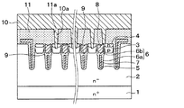
図2に示すように、本実施形態にかかる半導体装置は、不純物濃度が高濃度とされたシリコン等の半導体材料によって構成されたn+型の半導体基板1を用いて形成されている。n+型の半導体基板1の表面上には、n+型の半導体基板1よりも不純物濃度が低濃度とされたn−型ドリフト層2が形成されている。
As shown in FIG. 2, the semiconductor device according to the present embodiment is formed by using an n +
また、n−型ドリフト層2の表層部の所望位置には、比較的不純物濃度が低く設定されたp型ボディ領域3が形成されている。p型ボディ領域3は、例えばn−型ドリフト層2に対してp型不純物をイオン注入することなどによって形成され、チャネル領域を形成するチャネル層としても機能する。p型ボディ領域3は、図1に示すように、後述する複数のトレンチゲート構造の間において、y方向を長手方向として形成されている。
Further, n - the desired position of the surface portion of the
p型ボディ領域3の表層部には、n−型ドリフト層2よりも不純物濃度が高濃度とされたソース領域に相当するn型不純物領域4が備えられている。また、n型不純物領域4には、コンタクトトレンチ4aが形成されており、このコンタクトトレンチ4aの底面においてp型ボディ領域3が露出した状態となっている。なお、ここでは図示しないが、p型ボディ領域3のうちの露出した部分に、ボディコンタクトとなるp+型コンタクト領域を形成することもできる。さらに、n型不純物領域4のうちのコンタクトトレンチ4aの側面に、ソースコンタクトとなるn+型コンタクト領域を形成することもできる。
The surface layer portion of the p-
また、n−型ドリフト層2の表層部のうち各p型ボディ領域3や各n型不純物領域4の間には、一方向を長手方向とする複数本のゲートトレンチ5が形成されている。このゲートトレンチ5はトレンチゲート構造を形成するためのトレンチであり、本実施形態では、各ゲートトレンチ5が等間隔に並行に並べられることでストライプ状のレイアウトとされている。
Further, a plurality of
ゲートトレンチ5は、p型ボディ領域3よりも深い位置まで、つまり基板表面側からn型不純物領域4およびp型ボディ領域3を貫通してn−型ドリフト層2まで達する深さとされている。また、本実施形態では、ゲートトレンチ5は、底部に向かうほど徐々に幅が狭くなり、底部が丸まった形状とされている。
The
ゲートトレンチ5の内壁面は、絶縁膜6によって覆われている。絶縁膜6については、単独の膜で構成されていても良いが、本実施形態の場合は、ゲートトレンチ5のうちの下方部分を覆っているシールド絶縁膜6aと上方部分を覆っているゲート絶縁膜6bとによって構成している。シールド絶縁膜6aは、ゲートトレンチ5の底部から下方部分の側面を覆い、ゲート絶縁膜6bは、ゲートトレンチ5の上方部分の側面を覆っている。本実施形態では、シールド絶縁膜6aをゲート絶縁膜6bよりも厚く形成してある。
The inner wall surface of the
また、ゲートトレンチ5内には、絶縁膜6を介してドープトPoly−Siによって構成されたシールド電極7およびゲート電極層8が積層されて二層構造となっている。シールド電極7は、ソース電位に固定されることで、ゲート−ドレイン間の容量を小さくし、縦型MOSFETの電気特性の向上を図るために形成されている。ゲート電極層8は、縦型MOSFETのスイッチング動作を行うもので、ゲート電圧印加時にゲートトレンチ5の側面のp型ボディ領域3にチャネル領域を形成する。
Further, in the
シールド電極7とゲート電極層8との間には中間絶縁膜9が形成されており、中間絶縁膜9によってシールド電極7とゲート電極層8とが絶縁されている。これらゲートトレンチ5、絶縁膜6、シールド電極7、ゲート電極層8および中間絶縁膜9によってトレンチゲート構造が構成されている。このトレンチゲート構造は、例えば図1の紙面左右方向を長手方向として、図1の紙面上下方向、図2で言えば紙面左右方向に複数本が並べられることでストライプ状のレイアウトとされている。
An intermediate
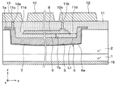
さらに、図3に示すように、ゲートトレンチ5の長手方向の両端部、すなわち図2の紙面手前側および紙面向こう側の端部において、シールド電極7は、ゲート電極層8よりも外側まで延設されている。そして、それらの部分がシールドライナー7aとしてp型ボディ領域3やn型不純物領域4の表面側から露出させられている。
Further, as shown in FIG. 3, the
また、ゲート電極層8を覆うように酸化膜などで構成された層間絶縁膜11が形成され、この層間絶縁膜11の上にソース電極に相当する上部電極10やゲート配線12およびシールド配線13が形成されている。上部電極10は、図2に示すように、層間絶縁膜11に形成されたコンタクトホール11a内に埋込まれたタングステン(W)プラグなどの接続部10aを通じてp型ボディ領域3やn型不純物領域4と接触させられている。これにより、上部電極10がn型不純物領域4およびp型ボディ領域3に電気的に接続されている。
Further, an
図3に示すように、ゲート配線12も、層間絶縁膜11に形成されたコンタクトホール11b内のWプラグなどの接続部12aを通じて、ゲート電極層8に電気的に接続されている。また、シールド配線13も、層間絶縁膜11に形成されたコンタクトホール11c内のWプラグなどの接続部13aを通じて、シールド電極7に電気的に接続されている。
As shown in FIG. 3, the
また、n+型の半導体基板1のうちn−型ドリフト層2とは反対側の面にドレイン電極に相当する下部電極15が形成されている。このような構成により、縦型MOSFETの基本構造が構成されている。そして、縦型MOSFETが複数セル集まって形成されることで、セル領域が構成されている。
Further, a
以上のようにして、縦型MOSFETを有する半導体装置が構成されている。そして、このように構成される縦型MOSFETにおいて、y方向、つまりトレンチゲート構造の長手方向の両先端のゲート電極層8が部分的に除去され、その除去された部分が酸化膜などの埋込絶縁膜11dによって埋込まれている。これにより、y方向の両先端において、該y方向に沿うゲート電極層8の先端からシールド電極7までの実効絶縁距離Liが中間絶縁膜9のうちのゲート電極層8の底部に位置している部分の厚さTbより大きくなる。
As described above, the semiconductor device having the vertical MOSFET is configured. Then, in the vertical MOSFET configured in this way, the
これにより、中間絶縁膜9の形成され方が製造方法や工程バラツキによって変化したとしても、ゲート電極層8のうちの先端部での中間絶縁膜9の絶縁耐圧を確保することが可能となる。したがって、中間絶縁膜9の絶縁耐圧が低下することを抑制でき、狙った信頼性を確保することができる。
As a result, even if the forming method of the intermediate
ここで、実効絶縁距離Liとは、y方向に沿うゲート電極層8の先端からシールド電極7までの間において絶縁機能を発揮する部分の距離である。
Here, the effective insulation distance Li is the distance of the portion that exerts the insulation function from the tip of the
例えば、図3においては、y方向において、ゲート電極層8のうちの先端部が完全に除去されている。この場合、ゲート電極層8の先端からシールド電極7までの間の距離、つまり絶縁機能を発揮する埋込絶縁膜11dおよび中間絶縁膜9のy方向寸法が実効絶縁距離Liとなる。これに対して、図4に示すように、ゲート電極層8の先端部が残渣部8aとして残る場合もある。残渣部8aが残っていても、埋込絶縁膜11dおよび中間絶縁膜9が絶縁機能を発揮することから、y方向におけるゲート電極層8とシールド電極7との間の絶縁耐圧を確保することはできる。ただし、残渣部8aについてはほぼ導電体として機能することから、この部分については絶縁機能を発揮しない。したがって、残渣部8aが存在する場合には、y方向におけるゲート電極層8の先端からシールド電極7までの距離より残渣部8aの寸法分を差し引いた値が実効絶縁距離Liとなる。
For example, in FIG. 3, the tip portion of the
実効絶縁距離Liについては、少なくとも中間絶縁膜9のうちゲート電極層8の底部に位置する部分の厚さTbよりも大きくなっていれば良いが、ほぼ厚さTbに対して埋込絶縁膜11dの幅Wを足した値になっている。すなわち、製造バラツキなどに起因して中間絶縁膜9のうちゲート電極層8の先端に位置している部分の厚みTaは、部分的に厚みTbよりも小さくなり得るが、厚みTbと同程度になる。このため、実効絶縁距離Liは、厚みTbと同程度の厚みTaに対して幅Wを足した値になる。
The effective insulating distance Li may be at least larger than the thickness Tb of the portion of the intermediate
例えば、厚みTa、厚みTbは、200nm程度に設定される。また、幅Wについては、1μm以上、例えば3.4μmに設定される。この幅Wは、後述するようにエッチングによりゲート電極層8の先端部を除去したときの幅として設定され、エッチング時のマスク開口幅と横方向エッチング量とによって設定される。このように、ゲート電極層8の先端からシールド電極7までの実効絶縁距離Liを中間絶縁膜9のうちのゲート電極層8の底部に位置している部分の厚さTbより大きくしているため、中間絶縁膜9の絶縁耐圧が低下することを抑制できる。
For example, the thickness Ta and the thickness Tb are set to about 200 nm. The width W is set to 1 μm or more, for example, 3.4 μm. This width W is set as the width when the tip portion of the
参考として、TZDB波形を調べた。具体的には、ゲート電極層8に対してゲート電圧Gを印加すると共にシールド電極7をソース電圧に相当する接地電位とし、ゲート電圧Gを変化させたときのゲート電極層8とシールド電極7との間に流れる電流の変化を調べた。図5Aは、従来構造、つまりゲート電極層8のうちの先端部を除去していない構造のTZDB波形、図5Bは、本実施形態の構造のTZDB波形を示している。これらの図より、従来構造と比較して、本実施形態の構造の方が、絶縁破壊されるゲート電圧値が大きくなっており、同じゲート電圧Gのときの電流Iを小さい値に抑えられていた。このため、中間絶縁膜9の絶縁耐圧の低下を抑制できていることが判る。
As a reference, the TZDB waveform was examined. Specifically, the
次に、本実施形態にかかる半導体装置の製造方法について図6A〜図6J、図7A〜図7Jおよび図8A〜図8Fを参照して説明する。図6A〜図6Jおよび図7A〜図7Jは、半導体装置の製造方法における各工程と対応する断面図である。図8A〜図8Fは、各工程と対応するセル部の上面レイアウト図であるが、一部の工程のみについてのみ示してある。 Next, a method of manufacturing the semiconductor device according to the present embodiment will be described with reference to FIGS. 6A to 6J, FIGS. 7A to 7J, and FIGS. 8A to 8F. 6A to 6J and FIGS. 7A to 7J are cross-sectional views corresponding to each step in the method for manufacturing a semiconductor device. 8A to 8F are top layout views of the cell portion corresponding to each process, but only a part of the processes are shown.
〔図6A、図7Aに示す工程〕
まず、半導体基板1を用意し、半導体基板1の表面上にn−型ドリフト層2をエピタキシャル成長させることで、高濃度層に相当する半導体基板1の一面側にn−型ドリフト層2が形成された基板を用意する。次に、ゲートトレンチ5の形成予定領域が開口するハードマスク20を配置する。このときのハードマスク20の上面レイアウトは図8Aのようになる。その後、ハードマスク20をマスクとして用いたエッチングによりゲートトレンチ5を形成する。
[Steps shown in FIGS. 6A and 7A]
First, a
〔図6B、図7Bに示す工程〕
続いて、ハードマスク20を除去した後、熱酸化などによってゲートトレンチ5の内壁面を含めてn−型ドリフト層2の表面にシールド絶縁膜6aを形成する。
[Steps shown in FIGS. 6B and 7B]
Subsequently, after removing the
〔図6C、図7Cに示す工程〕
シールド絶縁膜6aの上にドープトポリシリコンを積んでからエッチバックし、ゲートトレンチ5の底部やゲートトレンチ5の端部などにドープトポリシリコンを残すことでシールド電極7やシールドライナー7aを形成する。また、最も外側に位置するゲートトレンチ5については、ドープトポリシリコンで埋込まれたままとし、シールドライナー7aとして使用する。なお、このときの上面レイアウトは図8Bのようになる。
[Steps shown in FIGS. 6C and 7C]
The
〔図6D、図7Dに示す工程〕
シールド絶縁膜6aのうちゲートトレンチ5の上部の側面上やn−型ドリフト層2の表面上に形成された部分をエッチングして除去する。そして、プラズマCVD(chemical vapor deposition)などで絶縁膜をデポジションすることでシールド電極7の上やゲートトレンチ5の上部の側面を覆ったのち、マスクを用いてシールド電極7やシールドライナー7aの上に形成された部分のみが残るようにエッチングする。これにより、中間絶縁膜9が形成される。
[Steps shown in FIGS. 6D and 7D]
Side surfaces and n the upper portion of the
〔図6E、図7Eに示す工程〕
熱酸化などによってゲートトレンチ5の上部の側面上などに絶縁膜を形成することで、ゲート絶縁膜6bが形成される。
[Steps shown in FIGS. 6E and 7E]
The
〔図6F、図7Fに示す工程〕
再びドープトポリシリコンを積んでから、エッチバックすることでゲートトレンチ5内にゲート電極層8を形成する。これにより、トレンチゲート構造が形成される。ゲート電極層8のうちの一部については、ゲート配線12に接続されるため、部分的に上方に突出した状態で残される。なお、このときの上面レイアウトは図8Cのようになる。
[Steps shown in FIGS. 6F and 7F]
The
〔図6G、図7Gに示す工程〕
p型不純物をイオン注入することにより、p型ボディ領域3を形成する。そして、n型不純物領域4の形成予定領域が開口する図示しないマスクを配置したのち、n型不純物をイオン注入することでn型不純物領域4を形成する。
[Steps shown in FIGS. 6G and 7G]
The p-
〔図6H、図7Hに示す工程〕
ゲート電極層8やゲート絶縁膜6bなどの表面を覆うようにマスク30を形成したのち、マスク30のうちの埋込絶縁膜11dの形成予定領域を開口させる。そして、マスク30で覆った状態でドープトポリシリコンをエッチングすることで、ゲート電極層8のうちの先端部を除去する。このときの上面レイアウトは図8Dのようになる。
[Steps shown in FIGS. 6H and 7H]
After the
このとき、ドープトポリシリコンが確実に除去されるように、オーバエッチング量を50%増加している。例えば、ドープトポリシリコンの厚みを1μmとしていた場合には、1.5μm分の厚みを除去できるエッチング量としている。また、このようにした場合、例えばマスク30の開口幅を0.4μmとしたとき、横方向エッチング量が1.5μmとなり、ゲート電極層8のうちの先端部を3.4μm除去することができる。
At this time, the amount of overetching is increased by 50% so that the doped polysilicon is surely removed. For example, when the thickness of doped polysilicon is set to 1 μm, the etching amount is set so that the thickness of 1.5 μm can be removed. Further, in this case, for example, when the opening width of the
なお、マスク30の開口位置によっては、図4に示したようにゲート電極層8のうちの先端部が全て除去されずに残渣部8aとして残り得るが、残渣部8aが残っていたとしても、実効絶縁距離Liを設定できるため問題ない。
Depending on the opening position of the
〔図6I、図7Iに示す工程〕
続いて、CVD等によって酸化膜などで構成される層間絶縁膜11を形成したのち、平坦化研磨を行って層間絶縁膜11の表面の平坦化を行う。これにより、ゲート電極層8のうちの先端部が除去されることで開口した部分にも、層間絶縁膜11が埋込まれ、この部分が埋込絶縁膜11dとなる。なお、このときの上面レイアウトは図8Dのようになる。
[Steps shown in FIGS. 6I and 7I]
Subsequently, after forming the
〔図6J、図7Jに示す工程〕
図示しないハードマスクを配置したのち、ハードマスクで覆った状態で層間絶縁膜11をエッチングすることで、層間絶縁膜11に対してコンタクトホール11a〜11cを形成する。これにより、n型不純物領域4の表面の一部が露出させられる。
[Steps shown in FIGS. 6J and 7J]
After arranging a hard mask (not shown), the
さらに、ハードマスクを除去したのち、層間絶縁膜11をマスクとしてシリコンエッチングを行い、コンタクトホール11aと対応する位置にコンタクトトレンチ4aを形成する。これにより、コンタクトトレンチ4aの底面においてp型ボディ領域3が露出させられる。
Further, after removing the hard mask, silicon etching is performed using the
〔図6K、図7Kに示す工程〕
配線加工工程として、コンタクトホール11a〜11c内に接続部10a、12a、13aを形成する工程と行う。そして、さらに層間絶縁膜11の表面にAl等の配線材料を成膜し、それをパターニングすることで上部電極10やゲート配線12およびシールド配線13を形成する。
[Steps shown in FIGS. 6K and 7K]
As a wiring processing step, a step of forming
最後に、下部電極15の形成工程を行う。このようにして、本実施形態にかかる縦型MOSFETを有する半導体装置が完成する。
Finally, a step of forming the
以上説明したように、本実施形態の半導体装置では、ゲート電極層8の先端からシールド電極7までの実効絶縁距離Liを中間絶縁膜9のうちのゲート電極層8の底部に位置している部分の厚さTbより大きくしている。したがって、中間絶縁膜9の絶縁耐圧が低下することを抑制でき、狙った信頼性を確保することができる。
As described above, in the semiconductor device of the present embodiment, the effective insulation distance Li from the tip of the
(他の実施形態)
本開示は、上記した実施形態に準拠して記述されたが、当該実施形態に限定されるものではなく、様々な変形例や均等範囲内の変形をも包含する。加えて、様々な組み合わせや形態、さらには、それらに一要素のみ、それ以上、あるいはそれ以下、を含む他の組み合わせや形態をも、本開示の範疇や思想範囲に入るものである。
(Other embodiments)
Although the present disclosure has been described in accordance with the above-described embodiment, the present disclosure is not limited to the embodiment, and includes various modifications and modifications within a uniform range. In addition, various combinations and forms, as well as other combinations and forms that include only one element, more, or less, are within the scope and scope of the present disclosure.
(1)例えば、上記実施形態では、半導体基板1によって高濃度の不純物領域を形成し、その上にn−型ドリフト層2をエピタキシャル成長させることで、高濃度層とn−型ドリフト層2とが形成された基板を構成している。これは、ドリフト層を挟んでp型ボディ領域3と反対側に高濃度層を構成する場合の一例を示したに過ぎず、ドリフト層を半導体基板によって構成し、その一面側にイオン注入等を行うことで高濃度層を形成するようにしても良い。
(1) For example, in the above embodiment, the high-concentration layer and the n -
(2)また、上記実施形態では、トレンチゲート構造を形成してから、p型ボディ領域3やn型不純物領域4を形成したが、これらの形成順を逆にしても良い。すなわち、p型ボディ領域3やn型不純物領域4が最終的にトレンチゲート構造の間に位置する部分に形成されていれば良い。
(2) Further, in the above embodiment, the p-
(3)また、上記実施形態では、第1導電型をn型、第2導電型をp型としたnチャネルタイプのトレンチゲート構造のMOSFETを半導体スイッチング素子の一例として説明した。しかしながら、これは一例を示したに過ぎず、他の構造の半導体スイッチング素子、例えばnチャネルタイプに対して各構成要素の導電型を反転させたpチャネルタイプのトレンチゲート構造のMOSFETとしても良い。さらに、MOSFET以外に、同様の構造のIGBTに対しても本発明を適用することができる。IGBTの場合、半導体基板1の導電型をn型からp型に変更する以外は、上記実施形態で説明した縦型MOSFETと同様である。
(3) Further, in the above embodiment, a MOSFET having an n-channel type trench gate structure in which the first conductive type is n-type and the second conductive type is p-type has been described as an example of a semiconductor switching element. However, this is only an example, and a semiconductor switching element having another structure, for example, a MOSFET having a p-channel type trench gate structure in which the conductive type of each component is inverted with respect to the n-channel type may be used. Furthermore, the present invention can be applied to IGBTs having a similar structure other than MOSFETs. In the case of the IGBT, it is the same as the vertical MOSFET described in the above embodiment except that the conductive type of the
3 p型ボディ領域
4 n型不純物領域
6 絶縁膜
7 シールド電極
8 ゲート電極層
9 中間絶縁膜
10 上部電極
11 層間絶縁膜
11a 埋込絶縁膜
12 下部電極
3 p-type body region 4 n-
Claims (4)
前記半導体スイッチング素子は、
第1導電型のドリフト層(2)と、
前記ドリフト層上に形成された第2導電型のボディ領域(3)と、
前記ボディ領域内における該ボディ領域の表層部に形成され、前記ドリフト層より高不純物濃度とされた第1導電型の第1不純物領域(4)と、
一方向を長手方向とすると共に前記第1不純物領域から前記ボディ領域を貫通して前記ドリフト層に達する複数のトレンチ(5)内それぞれに、絶縁膜(6)を介して、シールド電極(7)と中間絶縁膜(9)およびゲート電極層(8)が順に積層されて二層構造とされた複数のトレンチゲート構造と、
前記ドリフト層を挟んで前記ボディ領域と反対側に形成され、前記ドリフト層よりも高不純物濃度とされた第1または第2導電型の高濃度層(1)と、
前記トレンチゲート構造と前記ボディ領域および前記第1不純物領域の上に配置され、前記ボディ領域や前記第1不純物領域に繋がるコンタクトホール(11a)が形成された層間絶縁膜(11)と、
前記コンタクトホールを通じて前記第1不純物領域および前記ボディ領域と電気的に接続される上部電極(10)と、
前記高濃度層と電気的に接続された下部電極(15)と、を有し、
前記シールド電極が前記ゲート電極層の先端部よりも外側まで延設されており、該シールド電極と前記ゲート電極層の底面との間に加えて前記ゲート電極層の先端部との間においても前記中間絶縁膜が形成されており、
前記一方向において、前記ゲート電極層の先端部から前記シールド電極までの間において絶縁機能を発揮する部分の距離となる実効絶縁距離(Li)が、前記中間絶縁膜のうち前記ゲート電極層の底部に位置している部分の厚み(Tb)よりも大きくなっていて、
前記一方向において、前記ゲート電極層の先端部と前記シールド電極との間に、前記中間絶縁膜および該中間絶縁膜と前記ゲート電極層の先端部との間に埋込まれた埋込絶縁膜(11d)のみが配置されており、
前記実効絶縁距離が、前記中間絶縁膜のうち前記ゲート電極層の先端部に位置している部分の厚さ(Ta)と前記埋込絶縁膜の幅(W)を足した値となっている、半導体装置。 A semiconductor device provided with a semiconductor switching element having a trench gate structure having a two-layer structure.
The semiconductor switching element is
The first conductive type drift layer (2) and
The second conductive type body region (3) formed on the drift layer and
A first conductive type first impurity region (4) formed on the surface layer portion of the body region in the body region and having a higher impurity concentration than the drift layer.
A shield electrode (7) is provided via an insulating film (6) in each of a plurality of trenches (5) having one direction as the longitudinal direction and penetrating the body region from the first impurity region to reach the drift layer. A plurality of trench gate structures in which the intermediate insulating film (9) and the gate electrode layer (8) are laminated in order to form a two-layer structure.
A first or second conductive type high-concentration layer (1) formed on the side opposite to the body region across the drift layer and having a higher impurity concentration than the drift layer.
An interlayer insulating film (11) arranged on the trench gate structure, the body region, and the first impurity region, and having a contact hole (11a) connected to the body region and the first impurity region.
An upper electrode (10) electrically connected to the first impurity region and the body region through the contact hole,
It has a lower electrode (15) electrically connected to the high concentration layer, and has.
The shield electrode extends to the outside of the tip of the gate electrode layer, and the shield electrode extends between the shield electrode and the bottom surface of the gate electrode layer as well as between the tip of the gate electrode layer. An intermediate insulating film is formed,
In the one direction, the effective insulation distance (Li), which is the distance between the tip of the gate electrode layer and the shield electrode, which is the distance of the portion that exerts the insulating function, is the bottom portion of the gate electrode layer in the intermediate insulating film. If you are greater than in that part of the thickness (Tb) located in,
In the one direction, the intermediate insulating film and the embedded insulating film embedded between the tip of the gate electrode layer and the shield electrode and the intermediate insulating film and the tip of the gate electrode layer are embedded. Only (11d) is arranged,
The effective insulating distance is a value obtained by adding the thickness (Ta) of the portion of the intermediate insulating film located at the tip of the gate electrode layer and the width (W) of the embedded insulating film. , Semiconductor device.
前記半導体スイッチング素子は、
第1導電型のドリフト層(2)と、
前記ドリフト層上に形成された第2導電型のボディ領域(3)と、
前記ボディ領域内における該ボディ領域の表層部に形成され、前記ドリフト層より高不純物濃度とされた第1導電型の第1不純物領域(4)と、
一方向を長手方向とすると共に前記第1不純物領域から前記ボディ領域を貫通して前記ドリフト層に達する複数のトレンチ(5)内それぞれに、絶縁膜(6)を介して、シールド電極(7)と中間絶縁膜(9)およびゲート電極層(8)が順に積層されて二層構造とされた複数のトレンチゲート構造と、
前記ドリフト層を挟んで前記ボディ領域と反対側に形成され、前記ドリフト層よりも高不純物濃度とされた第1または第2導電型の高濃度層(1)と、
前記トレンチゲート構造と前記ボディ領域および前記第1不純物領域の上に配置され、前記ボディ領域や前記第1不純物領域に繋がるコンタクトホール(11a)が形成された層間絶縁膜(11)と、
前記コンタクトホールを通じて前記第1不純物領域および前記ボディ領域と電気的に接続される上部電極(10)と、
前記高濃度層と電気的に接続された下部電極(15)と、を有し、
前記シールド電極が前記ゲート電極層の先端部よりも外側まで延設されており、該シールド電極と前記ゲート電極層の底面との間に加えて前記ゲート電極層の先端部との間においても前記中間絶縁膜が形成されており、
前記一方向において、前記ゲート電極層の先端部から前記シールド電極までの間において絶縁機能を発揮する部分の距離となる実効絶縁距離(Li)が、前記中間絶縁膜のうち前記ゲート電極層の底部に位置している部分の厚み(Tb)よりも大きくなっていて、
前記一方向において、前記ゲート電極層の先端部と前記シールド電極との間に、前記中間絶縁膜および該中間絶縁膜と前記ゲート電極層の先端部との間に埋込まれた埋込絶縁膜(11d)に加えて、前記ゲート電極層の一部で構成されかつ前記ゲート電極層から離れた残渣部(8a)が備えられており、
前記実効絶縁距離が、前記中間絶縁膜のうち前記ゲート電極層の先端部に位置している部分の厚さ(Ta)と前記埋込絶縁膜の幅(W)を足した値となっている、半導体装置。 A semiconductor device provided with a semiconductor switching element having a trench gate structure having a two-layer structure.
The semiconductor switching element is
The first conductive type drift layer (2) and
The second conductive type body region (3) formed on the drift layer and
A first conductive type first impurity region (4) formed on the surface layer portion of the body region in the body region and having a higher impurity concentration than the drift layer.
A shield electrode (7) is provided via an insulating film (6) in each of a plurality of trenches (5) having one direction as the longitudinal direction and penetrating the body region from the first impurity region to reach the drift layer. A plurality of trench gate structures in which the intermediate insulating film (9) and the gate electrode layer (8) are laminated in order to form a two-layer structure.
A first or second conductive type high-concentration layer (1) formed on the side opposite to the body region across the drift layer and having a higher impurity concentration than the drift layer.
An interlayer insulating film (11) arranged on the trench gate structure, the body region, and the first impurity region, and having a contact hole (11a) connected to the body region and the first impurity region.
An upper electrode (10) electrically connected to the first impurity region and the body region through the contact hole,
It has a lower electrode (15) electrically connected to the high concentration layer, and has.
The shield electrode extends to the outside of the tip of the gate electrode layer, and the shield electrode extends between the shield electrode and the bottom surface of the gate electrode layer as well as between the tip of the gate electrode layer. An intermediate insulating film is formed,
In the one direction, the effective insulation distance (Li), which is the distance between the tip of the gate electrode layer and the shield electrode, which is the distance of the portion that exerts the insulating function, is the bottom portion of the gate electrode layer in the intermediate insulating film. It is larger than the thickness (Tb) of the part located in
In the one direction, the intermediate insulating film and the embedded insulating film embedded between the tip of the gate electrode layer and the shield electrode and the intermediate insulating film and the tip of the gate electrode layer are embedded. In addition to (11d), a residue portion (8a) composed of a part of the gate electrode layer and separated from the gate electrode layer is provided.
The effective insulating distance is a value obtained by adding the thickness (Ta) of the portion of the intermediate insulating film located at the tip of the gate electrode layer and the width (W) of the embedded insulating film. , semi-conductor devices.
第1導電型または第2導電型の高濃度層(1)と、該高濃度層の一面側に形成され、該高濃度層よりも低不純物濃度とされた第1導電型のドリフト層(2)と、を有する基板(1、2)を用意することと、
前記ドリフト層に対して、一方向を長手方向とする複数のトレンチ(5)を形成したのち、該複数のトレンチ内それぞれに、絶縁膜(6)を介して、シールド電極(7)と中間絶縁膜(9)およびゲート電極層(8)を順に積層して二層構造の複数のトレンチゲート構造を形成することと、
前記複数のトレンチの間の位置における前記ドリフト層上に、第2導電型のボディ領域(3)を形成することと、
前記ボディ領域内における該ボディ領域の一部の表面部に、前記ドリフト層より高不純物濃度とされた第1導電型の第1不純物領域(4)を形成することと、
前記トレンチゲート構造と前記ボディ領域および前記第1不純物領域の上に層間絶縁膜(11)を形成することと、
前記層間絶縁膜に対して前記ボディ領域や前記第1不純物領域に繋がるコンタクトホール(11a)を形成することと、
前記コンタクトホールを通じて前記第1不純物領域および前記ボディ領域と電気的に接続される上部電極(10)を形成することと、
前記高濃度層と電気的に接続される下部電極(15)を形成することと、を含み、
前記トレンチゲート構造を形成することでは、
前記絶縁膜を介して、前記複数のトレンチの底面および前記一方向における該複数のトレンチの先端部に前記シールド電極を形成することと、
前記シールド電極の上に前記中間絶縁膜を形成することと、
前記中間絶縁膜の上に前記ゲート電極層を形成したのち、前記一方向における先端部において前記ゲート電極層を部分的に除去することと、
前記複数のトレンチ内における前記ゲート電極層が部分的に除去された部分を埋込絶縁膜(11d)で埋込むことと、を行う半導体装置の製造方法。 A method for manufacturing a semiconductor device including a semiconductor switching element having a trench gate structure.
A first conductive type or second conductive type high concentration layer (1) and a first conductive type drift layer (2) formed on one surface side of the high concentration layer and having a lower impurity concentration than the high concentration layer. ) And the substrate (1, 2) having
After forming a plurality of trenches (5) having a longitudinal direction in one direction with respect to the drift layer, intermediate insulation is provided with the shield electrode (7) in each of the plurality of trenches via an insulating film (6). The film (9) and the gate electrode layer (8) are laminated in order to form a plurality of trench gate structures having a two-layer structure.
Forming a second conductive type body region (3) on the drift layer at a position between the plurality of trenches, and
Forming a first conductive type first impurity region (4) having a higher impurity concentration than the drift layer on the surface portion of a part of the body region in the body region.
Forming an interlayer insulating film (11) on the trench gate structure, the body region, and the first impurity region,
By forming a contact hole (11a) connected to the body region and the first impurity region with respect to the interlayer insulating film,
Forming the upper electrode (10) electrically connected to the first impurity region and the body region through the contact hole, and
Including forming a lower electrode (15) that is electrically connected to the high concentration layer.
By forming the trench gate structure,
To form the shield electrode on the bottom surface of the plurality of trenches and the tip end portions of the plurality of trenches in one direction via the insulating film.
Forming the intermediate insulating film on the shield electrode and
After forming the gate electrode layer on the intermediate insulating film, the gate electrode layer is partially removed at the tip portion in the one direction.
A method for manufacturing a semiconductor device, wherein a portion of the plurality of trenches from which the gate electrode layer has been partially removed is embedded with an embedded insulating film (11d).
前記層間絶縁膜を形成することの際に、前記複数のトレンチ内における前記ゲート電極層が部分的に除去された部分に前記層間絶縁膜の一部を前記埋込絶縁膜として埋込むことである、請求項3に記載の半導体装置の製造方法。 Embedding with the embedded insulating film is
When forming the interlayer insulating film, a part of the interlayer insulating film is embedded as the embedded insulating film in a portion of the plurality of trenches from which the gate electrode layer is partially removed. , The method for manufacturing a semiconductor device according to claim 3.
Priority Applications (4)
| Application Number | Priority Date | Filing Date | Title |
|---|---|---|---|
| JP2019082275A JP6969586B2 (en) | 2019-04-23 | 2019-04-23 | Semiconductor devices and their manufacturing methods |
| PCT/JP2020/017393 WO2020218378A1 (en) | 2019-04-23 | 2020-04-22 | Semiconductor device, and manufacturing method therefor |
| CN202080030293.1A CN113767478B (en) | 2019-04-23 | 2020-04-22 | Semiconductor device and method for manufacturing the same |
| US17/505,747 US20220037523A1 (en) | 2019-04-23 | 2021-10-20 | Semiconductor device and method for manufacturing same |
Applications Claiming Priority (1)
| Application Number | Priority Date | Filing Date | Title |
|---|---|---|---|
| JP2019082275A JP6969586B2 (en) | 2019-04-23 | 2019-04-23 | Semiconductor devices and their manufacturing methods |
Publications (3)
| Publication Number | Publication Date |
|---|---|
| JP2020181854A JP2020181854A (en) | 2020-11-05 |
| JP2020181854A5 JP2020181854A5 (en) | 2021-05-06 |
| JP6969586B2 true JP6969586B2 (en) | 2021-11-24 |
Family
ID=72942609
Family Applications (1)
| Application Number | Title | Priority Date | Filing Date |
|---|---|---|---|
| JP2019082275A Active JP6969586B2 (en) | 2019-04-23 | 2019-04-23 | Semiconductor devices and their manufacturing methods |
Country Status (4)
| Country | Link |
|---|---|
| US (1) | US20220037523A1 (en) |
| JP (1) | JP6969586B2 (en) |
| CN (1) | CN113767478B (en) |
| WO (1) | WO2020218378A1 (en) |
Families Citing this family (3)
| Publication number | Priority date | Publication date | Assignee | Title |
|---|---|---|---|---|
| KR20220075811A (en) * | 2020-11-30 | 2022-06-08 | 현대자동차주식회사 | Semiconductor device and method manufacturing the same |
| CN114242765A (en) * | 2021-11-08 | 2022-03-25 | 深圳深爱半导体股份有限公司 | Semiconductor device structure and preparation method thereof |
| CN116895691A (en) * | 2023-05-31 | 2023-10-17 | 海信家电集团股份有限公司 | Semiconductor device and method for manufacturing the same |
Family Cites Families (13)
| Publication number | Priority date | Publication date | Assignee | Title |
|---|---|---|---|---|
| JP2005093773A (en) * | 2003-09-18 | 2005-04-07 | Fuji Electric Device Technology Co Ltd | Trench gate type semiconductor device and its manufacturing method |
| JP4039376B2 (en) * | 2004-03-09 | 2008-01-30 | 日産自動車株式会社 | Semiconductor device |
| JP2008218711A (en) * | 2007-03-05 | 2008-09-18 | Renesas Technology Corp | Semiconductor device, its manufacturing method, and power supply device |
| JP5580150B2 (en) * | 2010-09-09 | 2014-08-27 | 株式会社東芝 | Semiconductor device |
| JP5720582B2 (en) * | 2012-01-12 | 2015-05-20 | トヨタ自動車株式会社 | Switching element |
| US9293376B2 (en) * | 2012-07-11 | 2016-03-22 | Taiwan Semiconductor Manufacturing Company, Ltd. | Apparatus and method for power MOS transistor |
| WO2014168171A1 (en) * | 2013-04-11 | 2014-10-16 | 富士電機株式会社 | Semiconductor device and semiconductor device manufacturing method |
| JP6218423B2 (en) * | 2013-04-25 | 2017-10-25 | 三菱電機株式会社 | Silicon carbide semiconductor device and manufacturing method thereof |
| WO2016042738A1 (en) * | 2014-09-16 | 2016-03-24 | 株式会社デンソー | Silicon carbide semiconductor device and method for manufacturing same |
| JP2016062981A (en) * | 2014-09-16 | 2016-04-25 | 株式会社東芝 | Semiconductor device and manufacturing method of the same |
| JP6416056B2 (en) * | 2015-08-26 | 2018-10-31 | 株式会社東芝 | Semiconductor device |
| JP6528640B2 (en) * | 2015-10-22 | 2019-06-12 | 三菱電機株式会社 | Semiconductor device and method of manufacturing the same |
| JP6683083B2 (en) * | 2016-09-21 | 2020-04-15 | 株式会社デンソー | Semiconductor device and manufacturing method thereof |
-
2019
- 2019-04-23 JP JP2019082275A patent/JP6969586B2/en active Active
-
2020
- 2020-04-22 CN CN202080030293.1A patent/CN113767478B/en active Active
- 2020-04-22 WO PCT/JP2020/017393 patent/WO2020218378A1/en active Application Filing
-
2021
- 2021-10-20 US US17/505,747 patent/US20220037523A1/en active Pending
Also Published As
| Publication number | Publication date |
|---|---|
| WO2020218378A1 (en) | 2020-10-29 |
| JP2020181854A (en) | 2020-11-05 |
| US20220037523A1 (en) | 2022-02-03 |
| CN113767478B (en) | 2023-12-05 |
| CN113767478A (en) | 2021-12-07 |
Similar Documents
| Publication | Publication Date | Title |
|---|---|---|
| JP5587535B2 (en) | Semiconductor device | |
| WO2020218378A1 (en) | Semiconductor device, and manufacturing method therefor | |
| JP6666671B2 (en) | Semiconductor device | |
| US20110260241A1 (en) | Semiconductor Power Device Having a Top-side Drain Using a Sinker Trench | |
| CN101740622A (en) | Trench shielding structure for semiconductor device and method | |
| US9614073B2 (en) | Semiconductor device, and manufacturing method for same | |
| US20220165878A1 (en) | Semiconductor device | |
| CN101740612A (en) | Contact structure for semiconductor device having trench shield electrode and method | |
| JP4735235B2 (en) | Insulated gate semiconductor device and manufacturing method thereof | |
| JP2008501235A (en) | Semiconductor device and manufacturing method | |
| US20210242342A1 (en) | Semiconductor device and method for manufacturing same | |
| CN108962993A (en) | Semiconductor device and its manufacturing method | |
| US7005678B2 (en) | Silicon carbide semiconductor device having junction field effect transistor and method for manufacturing the same | |
| JP5616720B2 (en) | Semiconductor device and manufacturing method thereof | |
| JP6257525B2 (en) | Semiconductor device | |
| US20200312997A1 (en) | Semiconductor device | |
| JP6602698B2 (en) | Semiconductor device and manufacturing method thereof | |
| CN113410302A (en) | Semiconductor device with a plurality of semiconductor chips | |
| US20180366575A1 (en) | Semiconductor device | |
| JP7268514B2 (en) | semiconductor equipment | |
| TWI708342B (en) | Semiconductor structure and manufacturing method thereof and terminal area structure of semiconductor device | |
| JP2007067249A (en) | Semiconductor device and its manufacturing method | |
| US20230042721A1 (en) | Semiconductor device and manufacturing method of semiconductor device | |
| US20240113218A1 (en) | Semiconductor device and method of manufacturing the same | |
| JP2018081949A (en) | Semiconductor device and manufacturing method thereof |
Legal Events
| Date | Code | Title | Description |
|---|---|---|---|
| A521 | Request for written amendment filed |
Free format text: JAPANESE INTERMEDIATE CODE: A523 Effective date: 20210326 |
|
| A621 | Written request for application examination |
Free format text: JAPANESE INTERMEDIATE CODE: A621 Effective date: 20210326 |
|
| TRDD | Decision of grant or rejection written | ||
| A01 | Written decision to grant a patent or to grant a registration (utility model) |
Free format text: JAPANESE INTERMEDIATE CODE: A01 Effective date: 20210928 |
|
| A61 | First payment of annual fees (during grant procedure) |
Free format text: JAPANESE INTERMEDIATE CODE: A61 Effective date: 20211011 |
|
| R151 | Written notification of patent or utility model registration |
Ref document number: 6969586 Country of ref document: JP Free format text: JAPANESE INTERMEDIATE CODE: R151 |