JP6969586B2 - 半導体装置およびその製造方法 - Google Patents
半導体装置およびその製造方法 Download PDFInfo
- Publication number
- JP6969586B2 JP6969586B2 JP2019082275A JP2019082275A JP6969586B2 JP 6969586 B2 JP6969586 B2 JP 6969586B2 JP 2019082275 A JP2019082275 A JP 2019082275A JP 2019082275 A JP2019082275 A JP 2019082275A JP 6969586 B2 JP6969586 B2 JP 6969586B2
- Authority
- JP
- Japan
- Prior art keywords
- insulating film
- layer
- gate electrode
- body region
- electrode layer
- Prior art date
- Legal status (The legal status is an assumption and is not a legal conclusion. Google has not performed a legal analysis and makes no representation as to the accuracy of the status listed.)
- Active
Links
- 239000004065 semiconductor Substances 0.000 title claims description 76
- 238000004519 manufacturing process Methods 0.000 title claims description 48
- 239000010410 layer Substances 0.000 claims description 157
- 239000012535 impurity Substances 0.000 claims description 56
- 210000000746 body region Anatomy 0.000 claims description 55
- 239000011229 interlayer Substances 0.000 claims description 23
- 239000000758 substrate Substances 0.000 claims description 16
- 238000009413 insulation Methods 0.000 claims description 15
- 238000000034 method Methods 0.000 claims description 14
- 239000002344 surface layer Substances 0.000 claims description 6
- 230000000149 penetrating effect Effects 0.000 claims 2
- 238000005530 etching Methods 0.000 description 11
- 229910021420 polycrystalline silicon Inorganic materials 0.000 description 8
- 229920005591 polysilicon Polymers 0.000 description 7
- 230000015572 biosynthetic process Effects 0.000 description 3
- XUIMIQQOPSSXEZ-UHFFFAOYSA-N Silicon Chemical compound [Si] XUIMIQQOPSSXEZ-UHFFFAOYSA-N 0.000 description 2
- 238000005229 chemical vapour deposition Methods 0.000 description 2
- 238000010586 diagram Methods 0.000 description 2
- 239000000463 material Substances 0.000 description 2
- 238000012986 modification Methods 0.000 description 2
- 230000004048 modification Effects 0.000 description 2
- 230000003647 oxidation Effects 0.000 description 2
- 238000007254 oxidation reaction Methods 0.000 description 2
- 229910052710 silicon Inorganic materials 0.000 description 2
- 239000010703 silicon Substances 0.000 description 2
- 240000007594 Oryza sativa Species 0.000 description 1
- 235000007164 Oryza sativa Nutrition 0.000 description 1
- 230000015556 catabolic process Effects 0.000 description 1
- 239000004020 conductor Substances 0.000 description 1
- 230000002950 deficient Effects 0.000 description 1
- 230000001747 exhibiting effect Effects 0.000 description 1
- 230000002093 peripheral effect Effects 0.000 description 1
- 238000005268 plasma chemical vapour deposition Methods 0.000 description 1
- 238000005498 polishing Methods 0.000 description 1
- 235000009566 rice Nutrition 0.000 description 1
- 238000012216 screening Methods 0.000 description 1
- WFKWXMTUELFFGS-UHFFFAOYSA-N tungsten Chemical compound [W] WFKWXMTUELFFGS-UHFFFAOYSA-N 0.000 description 1
- 229910052721 tungsten Inorganic materials 0.000 description 1
- 239000010937 tungsten Substances 0.000 description 1
Images


Classifications
-
- H—ELECTRICITY
- H01—ELECTRIC ELEMENTS
- H01L—SEMICONDUCTOR DEVICES NOT COVERED BY CLASS H10
- H01L29/00—Semiconductor devices adapted for rectifying, amplifying, oscillating or switching, or capacitors or resistors with at least one potential-jump barrier or surface barrier, e.g. PN junction depletion layer or carrier concentration layer; Details of semiconductor bodies or of electrodes thereof ; Multistep manufacturing processes therefor
- H01L29/40—Electrodes ; Multistep manufacturing processes therefor
- H01L29/402—Field plates
- H01L29/407—Recessed field plates, e.g. trench field plates, buried field plates
-
- H—ELECTRICITY
- H01—ELECTRIC ELEMENTS
- H01L—SEMICONDUCTOR DEVICES NOT COVERED BY CLASS H10
- H01L29/00—Semiconductor devices adapted for rectifying, amplifying, oscillating or switching, or capacitors or resistors with at least one potential-jump barrier or surface barrier, e.g. PN junction depletion layer or carrier concentration layer; Details of semiconductor bodies or of electrodes thereof ; Multistep manufacturing processes therefor
- H01L29/02—Semiconductor bodies ; Multistep manufacturing processes therefor
- H01L29/06—Semiconductor bodies ; Multistep manufacturing processes therefor characterised by their shape; characterised by the shapes, relative sizes, or dispositions of the semiconductor regions ; characterised by the concentration or distribution of impurities within semiconductor regions
- H01L29/10—Semiconductor bodies ; Multistep manufacturing processes therefor characterised by their shape; characterised by the shapes, relative sizes, or dispositions of the semiconductor regions ; characterised by the concentration or distribution of impurities within semiconductor regions with semiconductor regions connected to an electrode not carrying current to be rectified, amplified or switched and such electrode being part of a semiconductor device which comprises three or more electrodes
- H01L29/1095—Body region, i.e. base region, of DMOS transistors or IGBTs
-
- H—ELECTRICITY
- H01—ELECTRIC ELEMENTS
- H01L—SEMICONDUCTOR DEVICES NOT COVERED BY CLASS H10
- H01L29/00—Semiconductor devices adapted for rectifying, amplifying, oscillating or switching, or capacitors or resistors with at least one potential-jump barrier or surface barrier, e.g. PN junction depletion layer or carrier concentration layer; Details of semiconductor bodies or of electrodes thereof ; Multistep manufacturing processes therefor
- H01L29/40—Electrodes ; Multistep manufacturing processes therefor
- H01L29/41—Electrodes ; Multistep manufacturing processes therefor characterised by their shape, relative sizes or dispositions
- H01L29/423—Electrodes ; Multistep manufacturing processes therefor characterised by their shape, relative sizes or dispositions not carrying the current to be rectified, amplified or switched
- H01L29/42312—Gate electrodes for field effect devices
- H01L29/42316—Gate electrodes for field effect devices for field-effect transistors
- H01L29/4232—Gate electrodes for field effect devices for field-effect transistors with insulated gate
- H01L29/42372—Gate electrodes for field effect devices for field-effect transistors with insulated gate characterised by the conducting layer, e.g. the length, the sectional shape or the lay-out
- H01L29/42376—Gate electrodes for field effect devices for field-effect transistors with insulated gate characterised by the conducting layer, e.g. the length, the sectional shape or the lay-out characterised by the length or the sectional shape
-
- H—ELECTRICITY
- H01—ELECTRIC ELEMENTS
- H01L—SEMICONDUCTOR DEVICES NOT COVERED BY CLASS H10
- H01L29/00—Semiconductor devices adapted for rectifying, amplifying, oscillating or switching, or capacitors or resistors with at least one potential-jump barrier or surface barrier, e.g. PN junction depletion layer or carrier concentration layer; Details of semiconductor bodies or of electrodes thereof ; Multistep manufacturing processes therefor
- H01L29/40—Electrodes ; Multistep manufacturing processes therefor
- H01L29/41—Electrodes ; Multistep manufacturing processes therefor characterised by their shape, relative sizes or dispositions
- H01L29/423—Electrodes ; Multistep manufacturing processes therefor characterised by their shape, relative sizes or dispositions not carrying the current to be rectified, amplified or switched
- H01L29/42312—Gate electrodes for field effect devices
- H01L29/42316—Gate electrodes for field effect devices for field-effect transistors
- H01L29/4232—Gate electrodes for field effect devices for field-effect transistors with insulated gate
- H01L29/42372—Gate electrodes for field effect devices for field-effect transistors with insulated gate characterised by the conducting layer, e.g. the length, the sectional shape or the lay-out
- H01L29/4238—Gate electrodes for field effect devices for field-effect transistors with insulated gate characterised by the conducting layer, e.g. the length, the sectional shape or the lay-out characterised by the surface lay-out
-
- H—ELECTRICITY
- H01—ELECTRIC ELEMENTS
- H01L—SEMICONDUCTOR DEVICES NOT COVERED BY CLASS H10
- H01L29/00—Semiconductor devices adapted for rectifying, amplifying, oscillating or switching, or capacitors or resistors with at least one potential-jump barrier or surface barrier, e.g. PN junction depletion layer or carrier concentration layer; Details of semiconductor bodies or of electrodes thereof ; Multistep manufacturing processes therefor
- H01L29/66—Types of semiconductor device ; Multistep manufacturing processes therefor
- H01L29/66007—Multistep manufacturing processes
- H01L29/66075—Multistep manufacturing processes of devices having semiconductor bodies comprising group 14 or group 13/15 materials
- H01L29/66227—Multistep manufacturing processes of devices having semiconductor bodies comprising group 14 or group 13/15 materials the devices being controllable only by the electric current supplied or the electric potential applied, to an electrode which does not carry the current to be rectified, amplified or switched, e.g. three-terminal devices
- H01L29/66409—Unipolar field-effect transistors
- H01L29/66477—Unipolar field-effect transistors with an insulated gate, i.e. MISFET
- H01L29/66674—DMOS transistors, i.e. MISFETs with a channel accommodating body or base region adjoining a drain drift region
- H01L29/66712—Vertical DMOS transistors, i.e. VDMOS transistors
- H01L29/66734—Vertical DMOS transistors, i.e. VDMOS transistors with a step of recessing the gate electrode, e.g. to form a trench gate electrode
-
- H—ELECTRICITY
- H01—ELECTRIC ELEMENTS
- H01L—SEMICONDUCTOR DEVICES NOT COVERED BY CLASS H10
- H01L29/00—Semiconductor devices adapted for rectifying, amplifying, oscillating or switching, or capacitors or resistors with at least one potential-jump barrier or surface barrier, e.g. PN junction depletion layer or carrier concentration layer; Details of semiconductor bodies or of electrodes thereof ; Multistep manufacturing processes therefor
- H01L29/66—Types of semiconductor device ; Multistep manufacturing processes therefor
- H01L29/68—Types of semiconductor device ; Multistep manufacturing processes therefor controllable by only the electric current supplied, or only the electric potential applied, to an electrode which does not carry the current to be rectified, amplified or switched
- H01L29/76—Unipolar devices, e.g. field effect transistors
- H01L29/772—Field effect transistors
- H01L29/78—Field effect transistors with field effect produced by an insulated gate
- H01L29/7801—DMOS transistors, i.e. MISFETs with a channel accommodating body or base region adjoining a drain drift region
- H01L29/7802—Vertical DMOS transistors, i.e. VDMOS transistors
- H01L29/7811—Vertical DMOS transistors, i.e. VDMOS transistors with an edge termination structure
-
- H—ELECTRICITY
- H01—ELECTRIC ELEMENTS
- H01L—SEMICONDUCTOR DEVICES NOT COVERED BY CLASS H10
- H01L29/00—Semiconductor devices adapted for rectifying, amplifying, oscillating or switching, or capacitors or resistors with at least one potential-jump barrier or surface barrier, e.g. PN junction depletion layer or carrier concentration layer; Details of semiconductor bodies or of electrodes thereof ; Multistep manufacturing processes therefor
- H01L29/66—Types of semiconductor device ; Multistep manufacturing processes therefor
- H01L29/68—Types of semiconductor device ; Multistep manufacturing processes therefor controllable by only the electric current supplied, or only the electric potential applied, to an electrode which does not carry the current to be rectified, amplified or switched
- H01L29/76—Unipolar devices, e.g. field effect transistors
- H01L29/772—Field effect transistors
- H01L29/78—Field effect transistors with field effect produced by an insulated gate
- H01L29/7801—DMOS transistors, i.e. MISFETs with a channel accommodating body or base region adjoining a drain drift region
- H01L29/7802—Vertical DMOS transistors, i.e. VDMOS transistors
- H01L29/7813—Vertical DMOS transistors, i.e. VDMOS transistors with trench gate electrode, e.g. UMOS transistors
-
- H—ELECTRICITY
- H01—ELECTRIC ELEMENTS
- H01L—SEMICONDUCTOR DEVICES NOT COVERED BY CLASS H10
- H01L29/00—Semiconductor devices adapted for rectifying, amplifying, oscillating or switching, or capacitors or resistors with at least one potential-jump barrier or surface barrier, e.g. PN junction depletion layer or carrier concentration layer; Details of semiconductor bodies or of electrodes thereof ; Multistep manufacturing processes therefor
- H01L29/02—Semiconductor bodies ; Multistep manufacturing processes therefor
- H01L29/06—Semiconductor bodies ; Multistep manufacturing processes therefor characterised by their shape; characterised by the shapes, relative sizes, or dispositions of the semiconductor regions ; characterised by the concentration or distribution of impurities within semiconductor regions
- H01L29/0684—Semiconductor bodies ; Multistep manufacturing processes therefor characterised by their shape; characterised by the shapes, relative sizes, or dispositions of the semiconductor regions ; characterised by the concentration or distribution of impurities within semiconductor regions characterised by the shape, relative sizes or dispositions of the semiconductor regions or junctions between the regions
- H01L29/0692—Surface layout
- H01L29/0696—Surface layout of cellular field-effect devices, e.g. multicellular DMOS transistors or IGBTs
-
- H—ELECTRICITY
- H01—ELECTRIC ELEMENTS
- H01L—SEMICONDUCTOR DEVICES NOT COVERED BY CLASS H10
- H01L29/00—Semiconductor devices adapted for rectifying, amplifying, oscillating or switching, or capacitors or resistors with at least one potential-jump barrier or surface barrier, e.g. PN junction depletion layer or carrier concentration layer; Details of semiconductor bodies or of electrodes thereof ; Multistep manufacturing processes therefor
- H01L29/40—Electrodes ; Multistep manufacturing processes therefor
- H01L29/41—Electrodes ; Multistep manufacturing processes therefor characterised by their shape, relative sizes or dispositions
- H01L29/417—Electrodes ; Multistep manufacturing processes therefor characterised by their shape, relative sizes or dispositions carrying the current to be rectified, amplified or switched
- H01L29/41725—Source or drain electrodes for field effect devices
- H01L29/41766—Source or drain electrodes for field effect devices with at least part of the source or drain electrode having contact below the semiconductor surface, e.g. the source or drain electrode formed at least partially in a groove or with inclusions of conductor inside the semiconductor
-
- H—ELECTRICITY
- H01—ELECTRIC ELEMENTS
- H01L—SEMICONDUCTOR DEVICES NOT COVERED BY CLASS H10
- H01L29/00—Semiconductor devices adapted for rectifying, amplifying, oscillating or switching, or capacitors or resistors with at least one potential-jump barrier or surface barrier, e.g. PN junction depletion layer or carrier concentration layer; Details of semiconductor bodies or of electrodes thereof ; Multistep manufacturing processes therefor
- H01L29/66—Types of semiconductor device ; Multistep manufacturing processes therefor
- H01L29/68—Types of semiconductor device ; Multistep manufacturing processes therefor controllable by only the electric current supplied, or only the electric potential applied, to an electrode which does not carry the current to be rectified, amplified or switched
- H01L29/70—Bipolar devices
- H01L29/72—Transistor-type devices, i.e. able to continuously respond to applied control signals
- H01L29/739—Transistor-type devices, i.e. able to continuously respond to applied control signals controlled by field-effect, e.g. bipolar static induction transistors [BSIT]
- H01L29/7393—Insulated gate bipolar mode transistors, i.e. IGBT; IGT; COMFET
- H01L29/7395—Vertical transistors, e.g. vertical IGBT
- H01L29/7396—Vertical transistors, e.g. vertical IGBT with a non planar surface, e.g. with a non planar gate or with a trench or recess or pillar in the surface of the emitter, base or collector region for improving current density or short circuiting the emitter and base regions
- H01L29/7397—Vertical transistors, e.g. vertical IGBT with a non planar surface, e.g. with a non planar gate or with a trench or recess or pillar in the surface of the emitter, base or collector region for improving current density or short circuiting the emitter and base regions and a gate structure lying on a slanted or vertical surface or formed in a groove, e.g. trench gate IGBT
Description
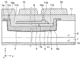
第1実施形態について説明する。本実施形態では、二層構造のトレンチゲート構造を有するnチャネルタイプのMOSFETが備えられた半導体装置を例に挙げて説明する。以下、図1〜図3に基づいて本実施形態にかかる半導体装置の構造について説明する。
まず、半導体基板1を用意し、半導体基板1の表面上にn−型ドリフト層2をエピタキシャル成長させることで、高濃度層に相当する半導体基板1の一面側にn−型ドリフト層2が形成された基板を用意する。次に、ゲートトレンチ5の形成予定領域が開口するハードマスク20を配置する。このときのハードマスク20の上面レイアウトは図8Aのようになる。その後、ハードマスク20をマスクとして用いたエッチングによりゲートトレンチ5を形成する。
続いて、ハードマスク20を除去した後、熱酸化などによってゲートトレンチ5の内壁面を含めてn−型ドリフト層2の表面にシールド絶縁膜6aを形成する。
シールド絶縁膜6aの上にドープトポリシリコンを積んでからエッチバックし、ゲートトレンチ5の底部やゲートトレンチ5の端部などにドープトポリシリコンを残すことでシールド電極7やシールドライナー7aを形成する。また、最も外側に位置するゲートトレンチ5については、ドープトポリシリコンで埋込まれたままとし、シールドライナー7aとして使用する。なお、このときの上面レイアウトは図8Bのようになる。
シールド絶縁膜6aのうちゲートトレンチ5の上部の側面上やn−型ドリフト層2の表面上に形成された部分をエッチングして除去する。そして、プラズマCVD(chemical vapor deposition)などで絶縁膜をデポジションすることでシールド電極7の上やゲートトレンチ5の上部の側面を覆ったのち、マスクを用いてシールド電極7やシールドライナー7aの上に形成された部分のみが残るようにエッチングする。これにより、中間絶縁膜9が形成される。
熱酸化などによってゲートトレンチ5の上部の側面上などに絶縁膜を形成することで、ゲート絶縁膜6bが形成される。
再びドープトポリシリコンを積んでから、エッチバックすることでゲートトレンチ5内にゲート電極層8を形成する。これにより、トレンチゲート構造が形成される。ゲート電極層8のうちの一部については、ゲート配線12に接続されるため、部分的に上方に突出した状態で残される。なお、このときの上面レイアウトは図8Cのようになる。
p型不純物をイオン注入することにより、p型ボディ領域3を形成する。そして、n型不純物領域4の形成予定領域が開口する図示しないマスクを配置したのち、n型不純物をイオン注入することでn型不純物領域4を形成する。
ゲート電極層8やゲート絶縁膜6bなどの表面を覆うようにマスク30を形成したのち、マスク30のうちの埋込絶縁膜11dの形成予定領域を開口させる。そして、マスク30で覆った状態でドープトポリシリコンをエッチングすることで、ゲート電極層8のうちの先端部を除去する。このときの上面レイアウトは図8Dのようになる。
続いて、CVD等によって酸化膜などで構成される層間絶縁膜11を形成したのち、平坦化研磨を行って層間絶縁膜11の表面の平坦化を行う。これにより、ゲート電極層8のうちの先端部が除去されることで開口した部分にも、層間絶縁膜11が埋込まれ、この部分が埋込絶縁膜11dとなる。なお、このときの上面レイアウトは図8Dのようになる。
図示しないハードマスクを配置したのち、ハードマスクで覆った状態で層間絶縁膜11をエッチングすることで、層間絶縁膜11に対してコンタクトホール11a〜11cを形成する。これにより、n型不純物領域4の表面の一部が露出させられる。
配線加工工程として、コンタクトホール11a〜11c内に接続部10a、12a、13aを形成する工程と行う。そして、さらに層間絶縁膜11の表面にAl等の配線材料を成膜し、それをパターニングすることで上部電極10やゲート配線12およびシールド配線13を形成する。
本開示は、上記した実施形態に準拠して記述されたが、当該実施形態に限定されるものではなく、様々な変形例や均等範囲内の変形をも包含する。加えて、様々な組み合わせや形態、さらには、それらに一要素のみ、それ以上、あるいはそれ以下、を含む他の組み合わせや形態をも、本開示の範疇や思想範囲に入るものである。
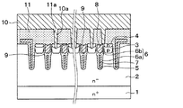
4 n型不純物領域
6 絶縁膜
7 シールド電極
8 ゲート電極層
9 中間絶縁膜
10 上部電極
11 層間絶縁膜
11a 埋込絶縁膜
12 下部電極
Claims (4)
- 二層構造のトレンチゲート構造を有する半導体スイッチング素子を備えた半導体装置であって、
前記半導体スイッチング素子は、
第1導電型のドリフト層(2)と、
前記ドリフト層上に形成された第2導電型のボディ領域(3)と、
前記ボディ領域内における該ボディ領域の表層部に形成され、前記ドリフト層より高不純物濃度とされた第1導電型の第1不純物領域(4)と、
一方向を長手方向とすると共に前記第1不純物領域から前記ボディ領域を貫通して前記ドリフト層に達する複数のトレンチ(5)内それぞれに、絶縁膜(6)を介して、シールド電極(7)と中間絶縁膜(9)およびゲート電極層(8)が順に積層されて二層構造とされた複数のトレンチゲート構造と、
前記ドリフト層を挟んで前記ボディ領域と反対側に形成され、前記ドリフト層よりも高不純物濃度とされた第1または第2導電型の高濃度層(1)と、
前記トレンチゲート構造と前記ボディ領域および前記第1不純物領域の上に配置され、前記ボディ領域や前記第1不純物領域に繋がるコンタクトホール(11a)が形成された層間絶縁膜(11)と、
前記コンタクトホールを通じて前記第1不純物領域および前記ボディ領域と電気的に接続される上部電極(10)と、
前記高濃度層と電気的に接続された下部電極(15)と、を有し、
前記シールド電極が前記ゲート電極層の先端部よりも外側まで延設されており、該シールド電極と前記ゲート電極層の底面との間に加えて前記ゲート電極層の先端部との間においても前記中間絶縁膜が形成されており、
前記一方向において、前記ゲート電極層の先端部から前記シールド電極までの間において絶縁機能を発揮する部分の距離となる実効絶縁距離(Li)が、前記中間絶縁膜のうち前記ゲート電極層の底部に位置している部分の厚み(Tb)よりも大きくなっていて、
前記一方向において、前記ゲート電極層の先端部と前記シールド電極との間に、前記中間絶縁膜および該中間絶縁膜と前記ゲート電極層の先端部との間に埋込まれた埋込絶縁膜(11d)のみが配置されており、
前記実効絶縁距離が、前記中間絶縁膜のうち前記ゲート電極層の先端部に位置している部分の厚さ(Ta)と前記埋込絶縁膜の幅(W)を足した値となっている、半導体装置。 - 二層構造のトレンチゲート構造を有する半導体スイッチング素子を備えた半導体装置であって、
前記半導体スイッチング素子は、
第1導電型のドリフト層(2)と、
前記ドリフト層上に形成された第2導電型のボディ領域(3)と、
前記ボディ領域内における該ボディ領域の表層部に形成され、前記ドリフト層より高不純物濃度とされた第1導電型の第1不純物領域(4)と、
一方向を長手方向とすると共に前記第1不純物領域から前記ボディ領域を貫通して前記ドリフト層に達する複数のトレンチ(5)内それぞれに、絶縁膜(6)を介して、シールド電極(7)と中間絶縁膜(9)およびゲート電極層(8)が順に積層されて二層構造とされた複数のトレンチゲート構造と、
前記ドリフト層を挟んで前記ボディ領域と反対側に形成され、前記ドリフト層よりも高不純物濃度とされた第1または第2導電型の高濃度層(1)と、
前記トレンチゲート構造と前記ボディ領域および前記第1不純物領域の上に配置され、前記ボディ領域や前記第1不純物領域に繋がるコンタクトホール(11a)が形成された層間絶縁膜(11)と、
前記コンタクトホールを通じて前記第1不純物領域および前記ボディ領域と電気的に接続される上部電極(10)と、
前記高濃度層と電気的に接続された下部電極(15)と、を有し、
前記シールド電極が前記ゲート電極層の先端部よりも外側まで延設されており、該シールド電極と前記ゲート電極層の底面との間に加えて前記ゲート電極層の先端部との間においても前記中間絶縁膜が形成されており、
前記一方向において、前記ゲート電極層の先端部から前記シールド電極までの間において絶縁機能を発揮する部分の距離となる実効絶縁距離(Li)が、前記中間絶縁膜のうち前記ゲート電極層の底部に位置している部分の厚み(Tb)よりも大きくなっていて、
前記一方向において、前記ゲート電極層の先端部と前記シールド電極との間に、前記中間絶縁膜および該中間絶縁膜と前記ゲート電極層の先端部との間に埋込まれた埋込絶縁膜(11d)に加えて、前記ゲート電極層の一部で構成されかつ前記ゲート電極層から離れた残渣部(8a)が備えられており、
前記実効絶縁距離が、前記中間絶縁膜のうち前記ゲート電極層の先端部に位置している部分の厚さ(Ta)と前記埋込絶縁膜の幅(W)を足した値となっている、半導体装置。 - トレンチゲート構造を有する半導体スイッチング素子を備えた半導体装置の製造方法であって、
第1導電型または第2導電型の高濃度層(1)と、該高濃度層の一面側に形成され、該高濃度層よりも低不純物濃度とされた第1導電型のドリフト層(2)と、を有する基板(1、2)を用意することと、
前記ドリフト層に対して、一方向を長手方向とする複数のトレンチ(5)を形成したのち、該複数のトレンチ内それぞれに、絶縁膜(6)を介して、シールド電極(7)と中間絶縁膜(9)およびゲート電極層(8)を順に積層して二層構造の複数のトレンチゲート構造を形成することと、
前記複数のトレンチの間の位置における前記ドリフト層上に、第2導電型のボディ領域(3)を形成することと、
前記ボディ領域内における該ボディ領域の一部の表面部に、前記ドリフト層より高不純物濃度とされた第1導電型の第1不純物領域(4)を形成することと、
前記トレンチゲート構造と前記ボディ領域および前記第1不純物領域の上に層間絶縁膜(11)を形成することと、
前記層間絶縁膜に対して前記ボディ領域や前記第1不純物領域に繋がるコンタクトホール(11a)を形成することと、
前記コンタクトホールを通じて前記第1不純物領域および前記ボディ領域と電気的に接続される上部電極(10)を形成することと、
前記高濃度層と電気的に接続される下部電極(15)を形成することと、を含み、
前記トレンチゲート構造を形成することでは、
前記絶縁膜を介して、前記複数のトレンチの底面および前記一方向における該複数のトレンチの先端部に前記シールド電極を形成することと、
前記シールド電極の上に前記中間絶縁膜を形成することと、
前記中間絶縁膜の上に前記ゲート電極層を形成したのち、前記一方向における先端部において前記ゲート電極層を部分的に除去することと、
前記複数のトレンチ内における前記ゲート電極層が部分的に除去された部分を埋込絶縁膜(11d)で埋込むことと、を行う半導体装置の製造方法。 - 前記埋込絶縁膜で埋込むことは、
前記層間絶縁膜を形成することの際に、前記複数のトレンチ内における前記ゲート電極層が部分的に除去された部分に前記層間絶縁膜の一部を前記埋込絶縁膜として埋込むことである、請求項3に記載の半導体装置の製造方法。
Priority Applications (4)
| Application Number | Priority Date | Filing Date | Title |
|---|---|---|---|
| JP2019082275A JP6969586B2 (ja) | 2019-04-23 | 2019-04-23 | 半導体装置およびその製造方法 |
| CN202080030293.1A CN113767478B (zh) | 2019-04-23 | 2020-04-22 | 半导体装置及其制造方法 |
| PCT/JP2020/017393 WO2020218378A1 (ja) | 2019-04-23 | 2020-04-22 | 半導体装置およびその製造方法 |
| US17/505,747 US20220037523A1 (en) | 2019-04-23 | 2021-10-20 | Semiconductor device and method for manufacturing same |
Applications Claiming Priority (1)
| Application Number | Priority Date | Filing Date | Title |
|---|---|---|---|
| JP2019082275A JP6969586B2 (ja) | 2019-04-23 | 2019-04-23 | 半導体装置およびその製造方法 |
Publications (3)
| Publication Number | Publication Date |
|---|---|
| JP2020181854A JP2020181854A (ja) | 2020-11-05 |
| JP2020181854A5 JP2020181854A5 (ja) | 2021-05-06 |
| JP6969586B2 true JP6969586B2 (ja) | 2021-11-24 |
Family
ID=72942609
Family Applications (1)
| Application Number | Title | Priority Date | Filing Date |
|---|---|---|---|
| JP2019082275A Active JP6969586B2 (ja) | 2019-04-23 | 2019-04-23 | 半導体装置およびその製造方法 |
Country Status (4)
| Country | Link |
|---|---|
| US (1) | US20220037523A1 (ja) |
| JP (1) | JP6969586B2 (ja) |
| CN (1) | CN113767478B (ja) |
| WO (1) | WO2020218378A1 (ja) |
Families Citing this family (3)
| Publication number | Priority date | Publication date | Assignee | Title |
|---|---|---|---|---|
| KR20220075811A (ko) * | 2020-11-30 | 2022-06-08 | 현대자동차주식회사 | 반도체 소자 및 그 제조 방법 |
| CN114242765A (zh) * | 2021-11-08 | 2022-03-25 | 深圳深爱半导体股份有限公司 | 半导体器件结构及其制备方法 |
| CN116895691A (zh) * | 2023-05-31 | 2023-10-17 | 海信家电集团股份有限公司 | 半导体装置及其制作方法 |
Family Cites Families (13)
| Publication number | Priority date | Publication date | Assignee | Title |
|---|---|---|---|---|
| JP2005093773A (ja) * | 2003-09-18 | 2005-04-07 | Fuji Electric Device Technology Co Ltd | トレンチゲート型半導体装置およびその製造方法 |
| JP4039376B2 (ja) * | 2004-03-09 | 2008-01-30 | 日産自動車株式会社 | 半導体装置 |
| JP2008218711A (ja) * | 2007-03-05 | 2008-09-18 | Renesas Technology Corp | 半導体装置およびその製造方法、ならびに電源装置 |
| JP5580150B2 (ja) * | 2010-09-09 | 2014-08-27 | 株式会社東芝 | 半導体装置 |
| JP5720582B2 (ja) * | 2012-01-12 | 2015-05-20 | トヨタ自動車株式会社 | スイッチング素子 |
| US9293376B2 (en) * | 2012-07-11 | 2016-03-22 | Taiwan Semiconductor Manufacturing Company, Ltd. | Apparatus and method for power MOS transistor |
| EP2985790B1 (en) * | 2013-04-11 | 2021-06-09 | Fuji Electric Co., Ltd. | Semiconductor device and semiconductor device manufacturing method |
| JP6218423B2 (ja) * | 2013-04-25 | 2017-10-25 | 三菱電機株式会社 | 炭化珪素半導体装置およびその製造方法 |
| WO2016042738A1 (ja) * | 2014-09-16 | 2016-03-24 | 株式会社デンソー | 炭化珪素半導体装置およびその製造方法 |
| JP2016062981A (ja) * | 2014-09-16 | 2016-04-25 | 株式会社東芝 | 半導体装置及びその製造方法 |
| JP6416056B2 (ja) * | 2015-08-26 | 2018-10-31 | 株式会社東芝 | 半導体装置 |
| JP6528640B2 (ja) * | 2015-10-22 | 2019-06-12 | 三菱電機株式会社 | 半導体装置及びその製造方法 |
| JP6683083B2 (ja) * | 2016-09-21 | 2020-04-15 | 株式会社デンソー | 半導体装置およびその製造方法 |
-
2019
- 2019-04-23 JP JP2019082275A patent/JP6969586B2/ja active Active
-
2020
- 2020-04-22 CN CN202080030293.1A patent/CN113767478B/zh active Active
- 2020-04-22 WO PCT/JP2020/017393 patent/WO2020218378A1/ja active Application Filing
-
2021
- 2021-10-20 US US17/505,747 patent/US20220037523A1/en active Pending
Also Published As
| Publication number | Publication date |
|---|---|
| WO2020218378A1 (ja) | 2020-10-29 |
| CN113767478B (zh) | 2023-12-05 |
| US20220037523A1 (en) | 2022-02-03 |
| CN113767478A (zh) | 2021-12-07 |
| JP2020181854A (ja) | 2020-11-05 |
Similar Documents
| Publication | Publication Date | Title |
|---|---|---|
| JP5587535B2 (ja) | 半導体装置 | |
| WO2020218378A1 (ja) | 半導体装置およびその製造方法 | |
| JP6666671B2 (ja) | 半導体装置 | |
| US20110260241A1 (en) | Semiconductor Power Device Having a Top-side Drain Using a Sinker Trench | |
| CN101740622A (zh) | 用于半导体器件的屏蔽电极结构和方法 | |
| US9614073B2 (en) | Semiconductor device, and manufacturing method for same | |
| US20220165878A1 (en) | Semiconductor device | |
| CN101740612A (zh) | 用于具有槽屏蔽电极的半导体器件的接触结构和方法 | |
| JP4735235B2 (ja) | 絶縁ゲート型半導体装置およびその製造方法 | |
| JP2008501235A (ja) | 半導体装置及び製造方法 | |
| US20210242342A1 (en) | Semiconductor device and method for manufacturing same | |
| CN108962993A (zh) | 半导体装置及其制造方法 | |
| US7005678B2 (en) | Silicon carbide semiconductor device having junction field effect transistor and method for manufacturing the same | |
| JP5616720B2 (ja) | 半導体装置およびその製造方法 | |
| JP6257525B2 (ja) | 半導体装置 | |
| JP6602698B2 (ja) | 半導体装置及びその製造方法 | |
| US20200312997A1 (en) | Semiconductor device | |
| CN113410302A (zh) | 半导体装置 | |
| US20180366575A1 (en) | Semiconductor device | |
| JP7268514B2 (ja) | 半導体装置 | |
| TWI708342B (zh) | 半導體結構及其製造方法以及半導體元件的終端區結構 | |
| JP2007067249A (ja) | 半導体装置およびその製造方法 | |
| US20230042721A1 (en) | Semiconductor device and manufacturing method of semiconductor device | |
| US20240113218A1 (en) | Semiconductor device and method of manufacturing the same | |
| JP2016054324A (ja) | 半導体装置 |
Legal Events
| Date | Code | Title | Description |
|---|---|---|---|
| A521 | Request for written amendment filed |
Free format text: JAPANESE INTERMEDIATE CODE: A523 Effective date: 20210326 |
|
| A621 | Written request for application examination |
Free format text: JAPANESE INTERMEDIATE CODE: A621 Effective date: 20210326 |
|
| TRDD | Decision of grant or rejection written | ||
| A01 | Written decision to grant a patent or to grant a registration (utility model) |
Free format text: JAPANESE INTERMEDIATE CODE: A01 Effective date: 20210928 |
|
| A61 | First payment of annual fees (during grant procedure) |
Free format text: JAPANESE INTERMEDIATE CODE: A61 Effective date: 20211011 |
|
| R151 | Written notification of patent or utility model registration |
Ref document number: 6969586 Country of ref document: JP Free format text: JAPANESE INTERMEDIATE CODE: R151 |