JP6528640B2 - Semiconductor device and method of manufacturing the same - Google Patents
Semiconductor device and method of manufacturing the same Download PDFInfo
- Publication number
- JP6528640B2 JP6528640B2 JP2015208171A JP2015208171A JP6528640B2 JP 6528640 B2 JP6528640 B2 JP 6528640B2 JP 2015208171 A JP2015208171 A JP 2015208171A JP 2015208171 A JP2015208171 A JP 2015208171A JP 6528640 B2 JP6528640 B2 JP 6528640B2
- Authority
- JP
- Japan
- Prior art keywords
- base region
- trench
- conductivity type
- region
- corner
- Prior art date
- Legal status (The legal status is an assumption and is not a legal conclusion. Google has not performed a legal analysis and makes no representation as to the accuracy of the status listed.)
- Active
Links
- 239000004065 semiconductor Substances 0.000 title claims description 40
- 238000004519 manufacturing process Methods 0.000 title claims description 19
- 239000010410 layer Substances 0.000 claims description 43
- 239000012535 impurity Substances 0.000 claims description 37
- HBMJWWWQQXIZIP-UHFFFAOYSA-N silicon carbide Chemical compound [Si+]#[C-] HBMJWWWQQXIZIP-UHFFFAOYSA-N 0.000 claims description 17
- 229910010271 silicon carbide Inorganic materials 0.000 claims description 17
- 239000000758 substrate Substances 0.000 claims description 16
- 238000005530 etching Methods 0.000 claims description 9
- 238000000034 method Methods 0.000 claims description 9
- 230000000149 penetrating effect Effects 0.000 claims description 4
- 239000002344 surface layer Substances 0.000 claims description 4
- 239000011229 interlayer Substances 0.000 description 9
- 230000005684 electric field Effects 0.000 description 8
- 238000010586 diagram Methods 0.000 description 7
- 238000005468 ion implantation Methods 0.000 description 7
- VYPSYNLAJGMNEJ-UHFFFAOYSA-N Silicium dioxide Chemical compound O=[Si]=O VYPSYNLAJGMNEJ-UHFFFAOYSA-N 0.000 description 4
- 229910052814 silicon oxide Inorganic materials 0.000 description 4
- 238000002513 implantation Methods 0.000 description 3
- 239000000463 material Substances 0.000 description 3
- 238000001020 plasma etching Methods 0.000 description 3
- 229910000838 Al alloy Inorganic materials 0.000 description 2
- XKRFYHLGVUSROY-UHFFFAOYSA-N Argon Chemical compound [Ar] XKRFYHLGVUSROY-UHFFFAOYSA-N 0.000 description 2
- IJGRMHOSHXDMSA-UHFFFAOYSA-N Atomic nitrogen Chemical compound N#N IJGRMHOSHXDMSA-UHFFFAOYSA-N 0.000 description 2
- 229910052782 aluminium Inorganic materials 0.000 description 2
- 238000000137 annealing Methods 0.000 description 2
- 230000015572 biosynthetic process Effects 0.000 description 2
- 238000005229 chemical vapour deposition Methods 0.000 description 2
- 230000000694 effects Effects 0.000 description 2
- 239000007772 electrode material Substances 0.000 description 2
- 238000004518 low pressure chemical vapour deposition Methods 0.000 description 2
- 229910052757 nitrogen Inorganic materials 0.000 description 2
- 229910021420 polycrystalline silicon Inorganic materials 0.000 description 2
- 229920005591 polysilicon Polymers 0.000 description 2
- XAGFODPZIPBFFR-UHFFFAOYSA-N aluminium Chemical compound [Al] XAGFODPZIPBFFR-UHFFFAOYSA-N 0.000 description 1
- 229910052786 argon Inorganic materials 0.000 description 1
- 238000000151 deposition Methods 0.000 description 1
- 239000002019 doping agent Substances 0.000 description 1
- 230000005669 field effect Effects 0.000 description 1
- 239000007789 gas Substances 0.000 description 1
- 238000010438 heat treatment Methods 0.000 description 1
- 239000011261 inert gas Substances 0.000 description 1
- 150000002500 ions Chemical class 0.000 description 1
- 230000007257 malfunction Effects 0.000 description 1
- 229910044991 metal oxide Inorganic materials 0.000 description 1
- 150000004706 metal oxides Chemical class 0.000 description 1
- 230000003647 oxidation Effects 0.000 description 1
- 238000007254 oxidation reaction Methods 0.000 description 1
- 230000001590 oxidative effect Effects 0.000 description 1
- 238000000059 patterning Methods 0.000 description 1
- 238000000206 photolithography Methods 0.000 description 1
Images


Classifications
-
- H—ELECTRICITY
- H01—ELECTRIC ELEMENTS
- H01L—SEMICONDUCTOR DEVICES NOT COVERED BY CLASS H10
- H01L29/00—Semiconductor devices adapted for rectifying, amplifying, oscillating or switching, or capacitors or resistors with at least one potential-jump barrier or surface barrier, e.g. PN junction depletion layer or carrier concentration layer; Details of semiconductor bodies or of electrodes thereof ; Multistep manufacturing processes therefor
- H01L29/66—Types of semiconductor device ; Multistep manufacturing processes therefor
- H01L29/68—Types of semiconductor device ; Multistep manufacturing processes therefor controllable by only the electric current supplied, or only the electric potential applied, to an electrode which does not carry the current to be rectified, amplified or switched
- H01L29/76—Unipolar devices, e.g. field effect transistors
- H01L29/772—Field effect transistors
- H01L29/78—Field effect transistors with field effect produced by an insulated gate
- H01L29/7801—DMOS transistors, i.e. MISFETs with a channel accommodating body or base region adjoining a drain drift region
- H01L29/7802—Vertical DMOS transistors, i.e. VDMOS transistors
- H01L29/7813—Vertical DMOS transistors, i.e. VDMOS transistors with trench gate electrode, e.g. UMOS transistors
-
- H—ELECTRICITY
- H01—ELECTRIC ELEMENTS
- H01L—SEMICONDUCTOR DEVICES NOT COVERED BY CLASS H10
- H01L29/00—Semiconductor devices adapted for rectifying, amplifying, oscillating or switching, or capacitors or resistors with at least one potential-jump barrier or surface barrier, e.g. PN junction depletion layer or carrier concentration layer; Details of semiconductor bodies or of electrodes thereof ; Multistep manufacturing processes therefor
- H01L29/02—Semiconductor bodies ; Multistep manufacturing processes therefor
- H01L29/06—Semiconductor bodies ; Multistep manufacturing processes therefor characterised by their shape; characterised by the shapes, relative sizes, or dispositions of the semiconductor regions ; characterised by the concentration or distribution of impurities within semiconductor regions
- H01L29/0684—Semiconductor bodies ; Multistep manufacturing processes therefor characterised by their shape; characterised by the shapes, relative sizes, or dispositions of the semiconductor regions ; characterised by the concentration or distribution of impurities within semiconductor regions characterised by the shape, relative sizes or dispositions of the semiconductor regions or junctions between the regions
- H01L29/0692—Surface layout
- H01L29/0696—Surface layout of cellular field-effect devices, e.g. multicellular DMOS transistors or IGBTs
-
- H—ELECTRICITY
- H01—ELECTRIC ELEMENTS
- H01L—SEMICONDUCTOR DEVICES NOT COVERED BY CLASS H10
- H01L29/00—Semiconductor devices adapted for rectifying, amplifying, oscillating or switching, or capacitors or resistors with at least one potential-jump barrier or surface barrier, e.g. PN junction depletion layer or carrier concentration layer; Details of semiconductor bodies or of electrodes thereof ; Multistep manufacturing processes therefor
- H01L29/02—Semiconductor bodies ; Multistep manufacturing processes therefor
- H01L29/06—Semiconductor bodies ; Multistep manufacturing processes therefor characterised by their shape; characterised by the shapes, relative sizes, or dispositions of the semiconductor regions ; characterised by the concentration or distribution of impurities within semiconductor regions
- H01L29/10—Semiconductor bodies ; Multistep manufacturing processes therefor characterised by their shape; characterised by the shapes, relative sizes, or dispositions of the semiconductor regions ; characterised by the concentration or distribution of impurities within semiconductor regions with semiconductor regions connected to an electrode not carrying current to be rectified, amplified or switched and such electrode being part of a semiconductor device which comprises three or more electrodes
- H01L29/1095—Body region, i.e. base region, of DMOS transistors or IGBTs
Description
この発明は、トレンチゲート構造の絶縁ゲート型半導体装置に関するものである。 The present invention relates to an insulated gate semiconductor device having a trench gate structure.
パワーエレクトロニクス分野において、モータ等の負荷への電力供給を制御するスイッチング素子として、IGBT(Insulated Gate Bipolar Transistor)やMOSFET(Metal Oxide Semiconductor Field Effect Transistor)などの半導体装置が広く使用されている。電力制御用の絶縁ゲート型半導体装置の一つに、ゲート電極が半導体層に埋め込まれて形成されたトレンチゲート型MOSFETがある。 In the field of power electronics, semiconductor devices such as IGBTs (Insulated Gate Bipolar Transistors) and MOSFETs (Metal Oxide Semiconductor Field Effect Transistors) are widely used as switching elements for controlling power supply to loads such as motors. One of the insulated gate semiconductor devices for power control is a trench gate MOSFET formed by embedding a gate electrode in a semiconductor layer.
トレンチゲート型MOSFETでは、チャネル密度を向上させることによって低抵抗化を実現することが可能であり、特許文献1に記載のトレンチゲート型MOSFETではトレンチを格子状に形成し、低抵抗化を実現している。
ここで、トレンチゲート型MOSFETでは、トレンチ内にゲート絶縁膜を介して、ポリシリコン等からなるゲート電極を埋め込む構造となっており、トレンチに接するベース領域にチャネルを形成する。このトレンチゲート型MOSFETをオンさせるために、ゲート電極にベース領域が反転する電圧を印加し、ゲート電極に印加された電圧がゲート絶縁膜を介してベース領域に印加する。この電圧によって発生する電界によって、ベース領域内にチャネルが形成される。
In the trench gate type MOSFET, it is possible to realize low resistance by improving the channel density, and in the trench gate type MOSFET described in
Here, in the trench gate type MOSFET, a gate electrode made of polysilicon or the like is embedded in the trench via the gate insulating film, and a channel is formed in a base region in contact with the trench. In order to turn on this trench gate type MOSFET, a voltage that inverts the base region is applied to the gate electrode, and a voltage applied to the gate electrode is applied to the base region through the gate insulating film. The electric field generated by this voltage forms a channel in the base region.
トレンチを格子状に形成したトレンチゲート型MOSFETでは、格子によって交差部が発生する。交差部のチャネルには角部が存在する。ゲート電極に電圧を印加した場合、チャネルの角部には電界が集中することとなり、角部以外のゲート絶縁膜よりも大きな電界が印加される。したがって、角部のチャネルはそれ以外の箇所と比べて先にオン状態になってしまう。素子全体の閾値電圧は最も早くオン状態になった箇所で決まるため、結果として、素子全体の閾値電圧が低下してしまい、オン抵抗と閾値電圧のトレードオフの関係が悪化するとともに、低閾値電圧化によってシステムの誤動作を誘発する場合があった。 In a trench gate type MOSFET in which trenches are formed in a lattice, intersections are generated by the lattice. There are corners in the channel at the intersection. When a voltage is applied to the gate electrode, an electric field is concentrated at the corner of the channel, and an electric field larger than the gate insulating film other than the corner is applied. Therefore, the corner channel is turned on earlier than in the other places. Since the threshold voltage of the entire device is determined at the place where the device is turned on most quickly, as a result, the threshold voltage of the entire device is lowered, and the tradeoff relationship between the on resistance and the threshold voltage is deteriorated. Could lead to a malfunction of the system.
本発明は、上述のような問題を解決するためになされたもので、チャネル密度の大きな格子状のトレンチ構造を保持したまま、交差部の角部が先にオン状態となり、閾値電圧が低下するのを防ぎ、オン抵抗と閾値電圧のトレードオフの関係を改善した半導体装置を提供することを目的とする。 The present invention has been made to solve the above-mentioned problems, and the corner of the intersection is first turned on while the lattice trench structure having a large channel density is maintained, and the threshold voltage is lowered. To provide a semiconductor device in which the trade-off relationship between on-resistance and threshold voltage is improved.
本発明にかかる半導体装置は、半導体基板と、半導体基板上に設けられた第1導電型のドリフト層と、ドリフト層の表面側に位置する第2導電型の第1のベース領域と、第1のベース領域内に位置する第1導電型のソース領域と、第1のベース領域とソース領域を貫通し、複数の面からなるトレンチ側壁を有し、格子状に形成されたトレンチと、トレンチ内のトレンチ側壁に接して形成されたゲート絶縁膜と、トレンチ内にゲート絶縁膜を介して埋め込まれたゲート電極と、トレンチの交差部における角部に接する箇所には、角部以外のトレンチ側壁に接する箇所に形成された第1のベース領域の不純物濃度よりも高い不
純物濃度を有する、第2導電型の第2のベース領域とを備え、前記第2のベース領域は前記トレンチ側壁から0.1μm〜0.5μmの幅を持って形成されることを特徴とするものである。
A semiconductor device according to the present invention includes a semiconductor substrate, a drift layer of a first conductivity type provided on the semiconductor substrate, a first base region of a second conductivity type located on the surface side of the drift layer, and A source region of a first conductivity type located in the base region of the gate, a trench sidewall formed of a plurality of planes penetrating the first base region and the source region, and formed in a lattice shape; The gate insulating film formed in contact with the side wall of the trench, the gate electrode embedded in the trench via the gate insulating film, and the side wall of the trench other than the corner portion having a higher impurity concentration than the impurity concentration of the first base region formed in a portion in contact, and a second base region of a second conductivity type, said second base region 0.1μm from the trench sidewalls It is characterized in that is formed with a width of 0.5 [mu] m.
本発明にかかる半導体装置によれば、角部のゲート絶縁膜に接するベース領域の不純物濃度を角部以外より高くしているため、角部近傍に形成されるチャネルの部分的な閾値電圧を高くすることができ、角部が先にオン状態になるのを防ぐことができる。また、角部以外のチャネルを適切な閾値電圧に設定することができ、オン抵抗と閾値電圧のトレードオフを改善することができる。 According to the semiconductor device of the present invention, the impurity concentration of the base region in contact with the gate insulating film at the corner is made higher than that at other than the corner, so that the partial threshold voltage of the channel formed near the corner is high. It is possible to prevent the corner from turning on first. In addition, channels other than the corner can be set to appropriate threshold voltages, and the trade-off between on-resistance and threshold voltage can be improved.
実施の形態1.
まず、本発明の実施の形態1にかかる半導体装置の構成を説明する。
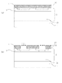
図1は、実施の形態1にかかる半導体装置であるトレンチゲート型MOSFETの活性領域の一部を模式的に示す上面図である。図1に示すように、本実施の形態のトレンチゲート型MOSFETの活性領域には、上面から見て正方形のセルが9個並んで配置されている部分がある。また、図2は、実施の形態1に係るトレンチゲート型MOSFETの活性領域の一部を模式的に示す断面図であり、図1の一点鎖線で示されるA−A断面図が図2(a)に対応し、図1の二点鎖線で示されるB−B断面図が図2(b)に対応する。ここで、B−B断面図は格子状に並ぶトレンチの交差部の特に角部を含む断面図となっている。
なお、図1においては、トレンチゲート型MOSFETのセルの構成が分かりやすいように、ソース電極、層間絶縁膜及びコンタクトホールは省略して示している。
First, the configuration of the semiconductor device according to the first embodiment of the present invention will be described.
FIG. 1 is a top view schematically showing a part of an active region of a trench gate type MOSFET which is a semiconductor device according to a first embodiment. As shown in FIG. 1, in the active region of the trench gate type MOSFET of the present embodiment, there is a portion in which nine square cells are arranged side by side as viewed from the top. 2 is a cross-sectional view schematically showing a part of the active region of the trench gate type MOSFET according to the first embodiment, and an AA cross-sectional view shown by an alternate long and short dash line in FIG. 1B corresponds to FIG. 2B, and a B-B cross-sectional view shown by a two-dot chain line in FIG. Here, the B-B cross-sectional view is a cross-sectional view including, in particular, corner portions of the intersections of the trenches arranged in a lattice.
In FIG. 1, the source electrode, the interlayer insulating film, and the contact hole are not shown so that the cell configuration of the trench gate type MOSFET can be easily understood.
本実施の形態にかかるトレンチ型MOSFETのセルの構成を、図1及び図2を参照して説明する。
本発明の実施の形態1に係る半導体装置であるトレンチ型MOSFETにおいては、低抵抗でn型の炭化珪素半導体基板1の第1の主面上に炭化珪素からなるn型のエピタキシャル層2が形成されている。エピタキシャル層2の表層部の一部には、炭化珪素からなるp型の第1のベース領域3が形成されている。エピタキシャル層2のうち、第1のベース領域3が形成されていない第1のベース領域3の下方の領域がドリフト層2aとなる。
The configuration of the cell of the trench MOSFET according to the present embodiment will be described with reference to FIGS. 1 and 2. FIG.
In the trench type MOSFET which is a semiconductor device according to the first embodiment of the present invention, n type
第1のベース領域3の表層部の一部にはn型のソース領域4が形成されている。第1のベース領域3およびソース領域4が形成された箇所のエピタキシャル層2に、ソース領域4と第1のベース領域3を貫通するように、トレンチ5が形成されている。トレンチ5は、上面から見て縦横に交差して、格子状に形成されている。隣接するトレンチ5との間は等間隔である。トレンチ5の底部は、第1のベース領域3より下方のドリフト層2aに達している。トレンチの内部には、底部と側壁を含む内壁を覆うように内壁に接してゲート絶縁膜6が形成されている。ゲート絶縁膜6のトレンチ内壁と反対側である内側には、ゲート電極7が形成されている。
An n-
エピタキシャル層2の表面には、ゲート電極7を覆うように層間絶縁膜8が形成されている。層間絶縁膜8には、ソース領域4および第1のベース領域3に達するコンタクトホール81が形成されている。層間絶縁膜8上に設けられたソース電極9はこのコンタクトホール81を埋めるように形成され、ソース領域4及び第1のベース領域3に接続される。なお、上述したとおり、図1ではエピタキシャル層2上の層間絶縁膜8、ソース電極9、コンタクトホール81を省略しているので、図1ではコンタクトホール81が示されていないが、図2に断面が示されたコンタクトホール81は、上面視で矩形の空間となっている。
また、炭化珪素半導体基板1の第1の主面の反対側の面である第2の主面には、ドレイン電極10が形成されている。
An
In addition,
図1に示すように、ゲート電極7は、上面視で格子状に配設されている。トレンチゲートMOSFETの活性領域内に設けられるセルでは、ゲート電極7で区切られた区画のそれぞれがトレンチゲート型MOSFETとして機能する。
また、図示はしないが、上面から見て活性領域の外側には終端領域が設けられており、トレンチゲート型MOSFETは、活性領域と終端領域とから構成されている。
As shown in FIG. 1, the
Although not shown, a termination region is provided outside the active region as viewed from the top, and the trench gate type MOSFET is composed of an active region and a termination region.
ここで、本実施の形態のトレンチゲート型MOSFETでは、図2(b)に示すように、格子状に形成されたトレンチの交差部に形成された角部に面して、p型の第2のベース領域14が形成されている。角部以外のトレンチ側壁に接する箇所には第2のベース領域14は形成されず、第1のベース領域3が形成されている。第2のベース領域の不純物濃度は第1のベース領域3の不純物濃度よりも高く設定している。
第2のベース領域14の幅、すなわち、トレンチ側壁からの距離は、チャネルが形成される幅以上であることが望ましく、例えば、0.1μm以上、0.5μm以下などであれば良い。
Here, in the trench gate type MOSFET according to the present embodiment, as shown in FIG. 2B, the p-type second MOSFET is faced to the corner portion formed at the intersection of the lattice-shaped trenches.
The width of the
次に、本実施の形態の半導体装置であるトレンチゲートMOSFETの動作について、説明する。
トレンチゲート型MOSFETにおいて、ゲート電極7に電圧が印加されると、ゲート絶縁膜6と接するベース領域3に電流が流れるチャネルが形成される。チャネルが形成されると、ドレイン電流が流れだす。一般的に、ある一定のドレイン電流が流れた時のゲート電圧を閾値電圧と定義している。
Next, the operation of the trench gate MOSFET which is the semiconductor device of the present embodiment will be described.
In the trench gate type MOSFET, when a voltage is applied to the
図3は、本実施の形態のトレンチゲート型MOSFETのゲート電圧に対するドレイン電流28を従来構造のトレンチゲート型MOSFETのドレイン電流29と比較して示したものである。ここで、従来構造のトレンチゲート型MOSFETとは、トレンチの交差部に第1のベース領域3の不純物濃度よりも高い第2のベース領域14が形成されていないもののことを言う。また、図3中、破線直線は閾値電圧を判定するドレイン電流値30である。
FIG. 3 shows the drain current 28 with respect to the gate voltage of the trench gate type MOSFET of the present embodiment in comparison with the drain current 29 of the trench gate type MOSFET of the conventional structure. Here, the conventional trench gate type MOSFET means that the
図3に示すように、従来構造のトレンチゲート型MOSFETでは、トレンチゲート型MOSFETの格子状に形成されたトレンチ5の交差部における角部に印加される電界が角部以外の箇所と比較して大きくなるため、角部近傍はそれ以外より先にオン状態となり、ドレイン電流29にこぶが発生してしまう。閾値電圧は、第1のベース領域3の不純物濃度にも依存し、第1のベース領域3の不純物濃度が高くなると、閾値電圧も高くなる。
As shown in FIG. 3, in the trench gate type MOSFET of the conventional structure, the electric field applied to the corner of the intersection of the
ここで、第2のベース領域14を形成するために注入するAlの不純物濃度及び第2のベース領域14の幅と効果の関係について説明しておく。
第2のベース領域14のp型(第2導電型)不純物濃度は、第1のベース領域3のp型(第2導電型)不純物濃度より高くする。この場合、トレンチ型MOSFETがオン状態になる際にチャネルが一定の幅を持って形成される。第2のベース領域14の幅が小さすぎると十分に閾値電圧を高くすることができず、角部のチャネルが先にオン状態となってしまうため、第2のベース領域14はチャネルによって反転する幅以上にする必要がある。さらに、第2のベース領域14のp型(第2導電型)不純物濃度が低いと、角部以外の閾値電圧よりも低くなってしまうため、角部に印加される電界において、オンしない不純物濃度以上にする必要がある。
Here, the relationship between the impurity concentration of Al implanted to form the
The p-type (second conductivity type) impurity concentration of the
第2のベース領域14のp型(第2導電型)不純物濃度と第1のベース領域3のp型(第2導電型)不純物濃度との関係については、その相対関係が重要である。例えば、第2のベース領域14のp型不純物濃度と第1のベース領域3の不純物濃度とは、その部分のMOSFETの局所的なVthが0.5V以上異なればよい。そのためには、例えば、第2のベース領域14の第2導電型不純物濃度が第1のベース領域3の第2導電型不純物濃度より5×1016cm−3以上高ければよい。このようにすれば、角部で先にチャネルがオンすることを防止できる。
The relationship between the p-type (second conductivity type) impurity concentration of the
本実施の形態のトレンチゲート型MOSFETでは、トレンチ5の交差部の角部近傍の第2のベース領域14のp型(第2導電型)不純物の濃度を第1のベース領域3のそれより高くしている。このため、トレンチ5の交差部の角部で角部以外と同じゲート電圧がゲート電極7に印加され、角部のゲート絶縁膜6に印加される電界が角部以外の箇所より大きくなった場合であっても、角部近傍の部分的な閾値電圧を高く設定できるため、角部が角部以外に対して先にオン状態となることがなく、閾値電圧の低下を防ぐことができる。したがって、図3に示すように、こぶが無く高い閾値電圧のドレイン電流−ゲート電圧特性を有するトレンチゲート型MOSFETを得ることができる。
In the trench gate type MOSFET according to the present embodiment, the concentration of the p-type (second conductivity type) impurity in the
つづいて、本実施の形態のトレンチゲート型MOSFETの製造方法を図4〜図10を用いて順次説明する。図4〜図10は、本実施の形態のトレンチゲート型MOSFETの製造方法を説明するための各工程のMOSFETの断面模式図である。また、図11は、図5の工程で第2のベース領域14を形成するためのイオン注入マスクの形状を示す平面図である。図4〜図10の各図の(a)および(b)は、それぞれ図1のA−A断面及びB−B断面に対応する断面図である。
Subsequently, a method of manufacturing the trench gate type MOSFET according to the present embodiment will be sequentially described with reference to FIGS. 4 to 10 are schematic cross-sectional views of the MOSFET in each step for illustrating the method of manufacturing the trench gate type MOSFET according to the present embodiment. FIG. 11 is a plan view showing the shape of an ion implantation mask for forming the
まず、図4に示すように、炭化珪素基板1上にエピタキシャル層2を形成する。ここでは4Hのポリタイプを有するn型(第1導電型)で低抵抗の炭化珪素基板1を用意し、その上に化学気相堆積(CVD:Chemical Vapor Deposition)法によりn型(第1導電型)の炭化珪素エピタキシャル層2をエピタキシャル成長させた。エピタキシャル層2のn型(第1導電型)不純物濃度は1×1015cm−3〜1×1017cm−3、厚さは5〜50μmとした。
First, as shown in FIG. 4,
つづいて、エピタキシャル層2の表面に所定のドーパントをイオン注入することにより、p型(第2導電型)の第1のベース領域3およびn型の(第1導電型)ソース領域4を形成する。ここでは、p型(第2導電型)の第1のベース領域3をp型(第2導電型)不純物であるアルミニウム(Al)のイオン注入により形成する。Alのイオン注入の深さは、エピタキシャル層2の厚さを超えない範囲で、0.5〜3μm程度とする。注入するAlの不純物濃度は、エピタキシャル層2のn型(第1導電型)不純物濃度より高くする。このとき、Alの注入深さよりも深いエピタキシャル層2の領域がドリフト層2aとなる。つまり、p型(第2導電型)の第1のベース領域3が形成されないエピタキシャル層2内の領域がドリフト層2aである。
Subsequently, p-type (second conductivity type)
n型(第1導電型)のソース領域4は、n型(第1導電型)不純物である窒素(N)を第1のベース領域3の表面にイオン注入することにより形成する。ソース領域4は、図1のように、この後形成されるゲート電極7(トレンチ5)のレイアウトに対応する格子状のパターンで形成される。従って、ゲート電極7が形成されたとき、ゲート電極7の両側にソース領域4が配設される。Nのイオン注入深さは、第1のベース領域3の厚さより浅くする。注入するNの不純物濃度は、第1のベース領域3のp型(第2導電型)不純物濃度よりも高くし、1×1018cm−3〜1×1021cm−3の範囲とする。
The n-type (first conductivity type)
次に、図5に示すように、第1の注入マスク16を介してp型(第2導電型)不純物であるAlをエピタキシャル層2の表面にイオン注入することにより、ソース領域4の下部にp型(第2導電型)の第2のベース領域14を形成する。第2のベース領域14はこの後形成されるトレンチの交差部における角部近傍に形成される。
図11は、本実施の形態に係るトレンチ型MOSFETの製造方法を説明するための上面図である。本実施の形態では、図5に示されるように、角部近傍が開口した第1の注入マスク16を介してイオン注入が行われて第2のベース領域14が形成される。
Next, as shown in FIG. 5, Al, which is a p-type (second conductivity type) impurity, is ion-implanted into the surface of the
FIG. 11 is a top view for illustrating the method for manufacturing the trench MOSFET according to the present embodiment. In the present embodiment, as shown in FIG. 5, the
第2のベース領域14は、この後形成されるトレンチ5のレイアウトに対応して、図5に示されるように、第2のベース領域14が形成される角部をまたぐように形成され、セルの配置に合わせて矩形状のパターンで形成される。また、第2のベース領域14の幅は第2のベース領域14を形成する角部のトレンチ側壁から同心円状に外側へ0.1μm以上0.5μm以下の幅を有するように形成する。
The
つづいて、図6に示すように、エピタキシャル層2の表面にシリコン酸化膜からなるエッチングマスク11を1〜2μm程度の厚さで堆積し、その上にレジスト材からなるレジストマスク12を形成する。レジストマスク12は、フォトリソグラフィー技術により、トレンチ5の形成領域を開口したパターンに形成される。トレンチ5が格子状なので、レジストマスク12はそれを反転したマトリクス状のパターンとなる。
Subsequently, as shown in FIG. 6, an
次に、図7に示すように、レジストマスク12をマスクとする反応性イオンエッチング(RIE:Reactive Ion Etching)処理により、エッチングマスク11をパターニングする。つまりレジストマスク12のパターンがシリコン酸化膜でできたエッチングマスク11に転写される。パターニングされたエッチングマスク11は次のトレンチ5を形成するエッチング工程におけるマスクとなる。
Next, as shown in FIG. 7, the
つづいて、図8に示すように、パターニングされたエッチングマスク11をマスクとするRIEにより、エピタキシャル層2にソース領域4および第1のベース領域3を貫通するトレンチ5を形成する。第1のベース領域3の一部には第2のベース領域14が形成されている。トレンチ5の深さは、ドリフト層2aに達するように第2のベース領域14が形成されている箇所より深くなるものとし、0.5〜3μm程度とする。
Subsequently, as shown in FIG. 8, a
次に、図8に示したレジストマスク12、および、エッチングマスク11を除去した後、熱処理装置を用いて、上記の工程でイオン注入したNおよびAlを活性化させるアニールを行う。このアニールは、アルゴン(Ar)ガスなどの不活性ガス雰囲気中で、1300〜1900℃、30秒〜1時間の条件で行なう。
Next, after removing the resist
つづいて、図9に示すように、トレンチ5の内側を含むエピタキシャル層2の全面にゲート絶縁膜6を形成した後、ゲート電極7となる低抵抗ポリシリコンを減圧CVD法により堆積し、それらをパターニングまたはエッチバックすることにより、トレンチ5内部にゲート絶縁膜6およびゲート電極7を形成する。ゲート絶縁膜6となるシリコン酸化膜は、エピタキシャル層2の表面を熱酸化法により熱酸化して形成してもよいし、エピタキシャル層2上及びトレンチ5の内側に堆積法により形成してもよい。
Subsequently, as shown in FIG. 9, after forming the
次に、図10に示すように、減圧CVD法により、エピタキシャル層2の表面全面にシリコン酸化膜からなる層間絶縁膜8を形成し、ゲート電極7を覆う。次に、層間絶縁膜8をパターニングすることで、ソース領域4および第1のベース領域3に達するコンタクトホール81を形成する。図10中、点線で囲まれた領域がコンタクトホール81に相当する。
Next, as shown in FIG. 10, an
そして、エピタキシャル層2上にAl合金等の電極材を堆積することで、層間絶縁膜8上並びにコンタクトホール81内に、ソース電極9を形成する。さらに、炭化珪素基板1の下面にAl合金等の電極材を堆積してドレイン電極10を形成することにより、図1、図2に示した構成のトレンチゲート型MOSFETを得ることができる。
Then, an electrode material such as an Al alloy is deposited on the
本実施の形態の半導体装置によれば、角部近傍の第2のベース領域14の不純物濃度を第1のベース領域3の不純物濃度よりも高くしているため、ゲート電極7に電圧を印加した際に格子状に配列されたトレンチの交差部における角部のゲート絶縁膜6に印加される電界がそれ以外の箇所より大きくなった場合であっても、角部近傍のチャネルの閾値電圧が角部以外のチャネルの閾値電圧より高くなるので、角部が角部以外に対して先にオン状態となることがなく、閾値電圧の低下を防ぐことができる。
According to the semiconductor device of the present embodiment, since the impurity concentration of the
なお、本実施の形態では、エピタキシャル層2と炭化珪素基板1とが同じ第1導電型を有する構造のトレンチ型MOSFETについて説明してきたが、本発明は、エピタキシャル層2と炭化珪素基板1とが異なる導電型を有する構造のトレンチゲート型IGBTに対しても適用可能である。例えば、図1に示したエピタキシャル層2が第1導電型のn型である構成に対し、炭化珪素基板1を第2導電型のp型にすればトレンチ型IGBTの構成となる。その場合、トレンチ型MOSFETのソース領域4およびソース電極9は、それぞれトレンチゲート型IGBTのエミッタ領域およびエミッタ電極に対応し、ドレイン電極10はコレクタ電極に対応することになる。
In the present embodiment, the trench type MOSFET having a structure in which
本実施の形態においては、炭化珪素半導体で構成された半導体装置を例として説明したが、半導体の材料は、他の材料であっても良く、また、他のワイドバンドギャップ半導体装置であっても良い。
また、本実施の形態では、第1導電型をn型、第2導電型をp型としたが、第1導電型をp型、第2導電型をn型としても良い。
In the present embodiment, the semiconductor device made of a silicon carbide semiconductor has been described as an example, but the material of the semiconductor may be another material, and even if it is another wide band gap semiconductor device good.
Further, in the present embodiment, although the first conductivity type is n-type and the second conductivity type is p-type, the first conductivity type may be p-type and the second conductivity type may be n-type.
さらに、本実施の形態においては、上面から見て正方形のセルを持つ活性領域の例について説明したが、セルは他の構造であってもよく、基本セルが長方形や六角形などであっても良い。また、セルの配置についても、縦横方向に規則正しく配置された例を用いて説明したが、隣接する列のセルがずれた配置であって、セルの角部に第2のベース領域が形成されていれば、同様の効果を奏する。また、第1のベース領域3と第2のベース領域の境界は、急峻でなくても良く、ある幅で連続的に不純物濃度が変化するものであってもよい。
Furthermore, in the present embodiment, an example of the active region having a square cell as viewed from the upper surface has been described, but the cell may have another structure, and the basic cell may be rectangular or hexagonal. good. Also, the arrangement of cells has been described using an example in which the cells are regularly arranged in the vertical and horizontal directions. However, the arrangement is such that the cells in adjacent columns are shifted, and the second base region is formed at the corner of the cells. Then, the same effect is achieved. Further, the boundary between the
また、製造方法においては、第1のベース領域3をエピタキシャル成長法によって形成してもよい。その場合も第1のベース領域3の不純物濃度および厚さは、イオン注入によって形成する場合と同等であれば良い。
In addition, in the manufacturing method, the
実施の形態2.
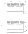
本発明の実施の形態2における炭化珪素半導体装置であるトレンチゲート型MOSFETの構成を説明する。図12と図13は、それぞれ本発明の実施の形態2に係る半導体装置であるトレンチゲート型MOSFETの活性領域の一部の上面図、活性領域の一部の断面模式図である。図12の一点鎖線で示されるA−A断面図が図13(a)に対応し、図1の二点鎖線で示されるB−B断面図が図13(b)に対応する。ここで、B−B断面図は格子状に並ぶトレンチの交差部の特に角部を含む断面図となっている。
Second Embodiment
The configuration of a trench gate type MOSFET which is a silicon carbide semiconductor device in a second embodiment of the present invention will be described. 12 and 13 are respectively a top view of a part of an active region of a trench gate type MOSFET which is a semiconductor device according to a second embodiment of the present invention, and a schematic sectional view of a part of the active region. An AA sectional view shown by an alternate long and short dash line in FIG. 12 corresponds to FIG. 13 (a), and a BB sectional view shown by an alternate long and two short dashes line in FIG. 1 corresponds to FIG. Here, the B-B cross-sectional view is a cross-sectional view including, in particular, corner portions of the intersections of the trenches arranged in a lattice.
図12と図13に示すように、本実施の形態のトレンチゲート型MOSFETは、格子状に形成されたトレンチの交差部において、実施の形態1で説明した第2のベース領域14を設ける代わりにソース領域4をトレンチ側壁から離して形成し、交差部以外の箇所ではソース領域4をトレンチ側壁に接するように形成している。その他の点については、実施の形態1と同様であるので、詳しい説明を省略する。
As shown in FIGS. 12 and 13, in the trench gate type MOSFET of the present embodiment, the
図12と図13に示すように、本実施の形態のトレンチゲート型MOSFETにおいては、トレンチの交差部で、ソース領域4をトレンチ側壁から離して形成しているが、その距離は、0.1μm以上などであれば良い。
As shown in FIGS. 12 and 13, in the trench gate type MOSFET of the present embodiment,
本実施の形態における半導体装置によれば、角部から離れた箇所にソース領域4が形成されているため、角部近傍のチャネル長が長くなり、閾値電圧が上昇し、かつ、チャネル抵抗が上昇する。つまり、角部近傍のチャネルがオンしにくくなる。したがって、ゲート電極7に電圧を印加した際に格子状に配列されたトレンチの交差部における角部のゲート絶縁膜6に印加される電界がそれ以外の箇所より大きくなった場合であっても、角部近傍のチャネルの部分的な閾値電圧が高くなり、チャネル抵抗が高くなるため、この部分による閾値電圧への影響を小さくなり、素子全体の閾値電圧が低下することを防ぐことができる。
According to the semiconductor device in the present embodiment, since
また、本実施の形態の半導体装置は、実施の形態1において第2のベース領域14を製造する工程を削除し、ソース領域4の形成領域を本実施の形態に示す形状にすれば製造できる。その他の点については、実施の形態1の半導体装置の製造方法と同様である。
The semiconductor device of the present embodiment can be manufactured by eliminating the step of manufacturing the
本発明の実施の形態2における半導体装置の製造方法によれば、本発明の実施の形態1における第2のベース領域14を形成工程が必要無くなるため、実施の形態1と比較してイオン注入工程を削減することができ、製造コストを低減した低コストの半導体装置を得ることができる。
According to the method for manufacturing a semiconductor device in the second embodiment of the present invention, the step of forming the
1 炭化珪素基板、2 エピタキシャル層、2a ドリフト層、3 第1のベース領域、4 ソース領域、5 トレンチ、6 ゲート絶縁膜、7 ゲート電極、8 層間絶縁膜、9 ソース電極、10 ドレイン電極、11 エッチングマスク、12 レジストマスク、14 第2のベース領域、81 コンタクトホール。 1 silicon carbide substrate, 2 epitaxial layer, 2a drift layer, 3 first base region, 4 source region, 5 trench, 6 gate insulating film, 7 gate electrode, 8 interlayer insulating film, 9 source electrode, 10 drain electrode, 11 Etch mask, 12 resist mask, 14 second base region, 81 contact holes.
Claims (5)
前記半導体基板上に設けられた第1導電型のドリフト層と、
前記ドリフト層の表面側に位置する第2導電型の第1のベース領域と、
前記第1のベース領域内に位置する第1導電型のソース領域と、
前記第1のベース領域と前記ソース領域を貫通し、複数の面からなるトレンチ側壁を有し、格子状に形成されたトレンチと、
前記トレンチ内の前記トレンチ側壁に接して形成されたゲート絶縁膜と、
前記トレンチ内に前記ゲート絶縁膜を介して埋め込まれたゲート電極と、
前記トレンチの交差部における角部に接する箇所に、前記角部以外の前記トレンチ側壁に接する箇所に形成された前記第1のベース領域の不純物濃度よりも高い不純物濃度を有する、第2導電型の第2のベース領域とを備え、
前記第2のベース領域は前記トレンチ側壁から0.1μm〜0.5μmの幅を持って形成されることを特徴とする半導体装置。 A semiconductor substrate,
A drift layer of the first conductivity type provided on the semiconductor substrate;
A first base region of the second conductivity type located on the surface side of the drift layer;
A source region of a first conductivity type located in the first base region;
A trench formed in a lattice shape, having a trench sidewall consisting of a plurality of planes penetrating the first base region and the source region;
A gate insulating film formed in contact with the side wall of the trench in the trench;
A gate electrode embedded in the trench via the gate insulating film;
The second conductivity type, having an impurity concentration higher than the impurity concentration of the first base region formed at a location in contact with the trench sidewall other than the corner at a location in contact with a corner in the intersection of the trench And a second base area ,
The semiconductor device characterized in that the second base region is formed with a width of 0.1 μm to 0.5 μm from the trench sidewall .
前記エピタキシャル層の表層部に第2導電型の第1のベース領域を形成する工程と、
前記第1のベース領域の表層部に第1導電型のソース領域を形成する工程と、
前記ドリフト層内に第1のベース領域より不純物濃度が高い、第2導電型の第2のベース領域を形成する工程と、
前記第1のベース領域と前記ソース領域を貫通するトレンチを、格子状に、前記トレンチの交差部における角部が前記第2のベース領域に接するように、前記第2のベース領域よりも深く、エッチングにより形成する工程と、
前記トレンチ内のトレンチ側壁に接するようにゲート絶縁膜を形成する工程と、
前記トレンチ内に前記ゲート絶縁膜を介してゲート電極を埋め込む工程と、
を備え、
前記第2のベース領域は前記トレンチ側壁から0.1μm〜0.5μmの幅を持って形成される半導体装置の製造方法。 Growing an epitaxial layer of a first conductivity type to be a drift layer of a first conductivity type on a semiconductor substrate;
Forming a first base region of the second conductivity type in a surface layer portion of the epitaxial layer;
Forming a source region of a first conductivity type in a surface layer portion of the first base region;
Forming in the drift layer a second base region of a second conductivity type, the impurity concentration of which is higher than that of the first base region;
The trench penetrating the first base region and the source region is formed in a grid shape, and is deeper than the second base region such that a corner at the intersection of the trenches contacts the second base region, Forming by etching;
Forming a gate insulating film in contact with a trench sidewall in the trench;
Embedding a gate electrode in the trench via the gate insulating film;
Equipped with
The method of manufacturing a semiconductor device, wherein the second base region is formed with a width of 0.1 μm to 0.5 μm from the trench sidewall .
Priority Applications (1)
| Application Number | Priority Date | Filing Date | Title |
|---|---|---|---|
| JP2015208171A JP6528640B2 (en) | 2015-10-22 | 2015-10-22 | Semiconductor device and method of manufacturing the same |
Applications Claiming Priority (1)
| Application Number | Priority Date | Filing Date | Title |
|---|---|---|---|
| JP2015208171A JP6528640B2 (en) | 2015-10-22 | 2015-10-22 | Semiconductor device and method of manufacturing the same |
Publications (3)
| Publication Number | Publication Date |
|---|---|
| JP2017084839A JP2017084839A (en) | 2017-05-18 |
| JP2017084839A5 JP2017084839A5 (en) | 2018-03-08 |
| JP6528640B2 true JP6528640B2 (en) | 2019-06-12 |
Family
ID=58713185
Family Applications (1)
| Application Number | Title | Priority Date | Filing Date |
|---|---|---|---|
| JP2015208171A Active JP6528640B2 (en) | 2015-10-22 | 2015-10-22 | Semiconductor device and method of manufacturing the same |
Country Status (1)
| Country | Link |
|---|---|
| JP (1) | JP6528640B2 (en) |
Cited By (1)
| Publication number | Priority date | Publication date | Assignee | Title |
|---|---|---|---|---|
| JP2022529411A (en) * | 2019-12-13 | 2022-06-22 | 華潤微電子(重慶)有限公司 | Structure of trench type field effect transistor and its manufacturing method |
Families Citing this family (2)
| Publication number | Priority date | Publication date | Assignee | Title |
|---|---|---|---|---|
| JP6969586B2 (en) * | 2019-04-23 | 2021-11-24 | 株式会社デンソー | Semiconductor devices and their manufacturing methods |
| US20230055891A1 (en) * | 2020-02-07 | 2023-02-23 | Infineon Technologies Austria Ag | Transistor Device and Method of Fabricating a Transistor Device |
Family Cites Families (4)
| Publication number | Priority date | Publication date | Assignee | Title |
|---|---|---|---|---|
| WO2000038244A1 (en) * | 1998-12-18 | 2000-06-29 | Infineon Technologies Ag | Field effect transistor arrangement with a trench gate electrode and an additional highly doped layer in the body region |
| JP3552208B2 (en) * | 2000-05-26 | 2004-08-11 | 株式会社東芝 | Semiconductor device |
| JP2004055976A (en) * | 2002-07-23 | 2004-02-19 | Toyota Industries Corp | Semiconductor device having trench structure |
| JP2013232533A (en) * | 2012-04-27 | 2013-11-14 | Rohm Co Ltd | Semiconductor device and semiconductor device manufacturing method |
-
2015
- 2015-10-22 JP JP2015208171A patent/JP6528640B2/en active Active
Cited By (3)
| Publication number | Priority date | Publication date | Assignee | Title |
|---|---|---|---|---|
| JP2022529411A (en) * | 2019-12-13 | 2022-06-22 | 華潤微電子(重慶)有限公司 | Structure of trench type field effect transistor and its manufacturing method |
| EP3933895A4 (en) * | 2019-12-13 | 2022-08-24 | China Resources Microelectronics (Chongqing) Co., Ltd | Trench field effect transistor structure, and manufacturing method for same |
| JP7368493B2 (en) | 2019-12-13 | 2023-10-24 | 華潤微電子(重慶)有限公司 | Structure of trench field effect transistor and manufacturing method thereof |
Also Published As
| Publication number | Publication date |
|---|---|
| JP2017084839A (en) | 2017-05-18 |
Similar Documents
| Publication | Publication Date | Title |
|---|---|---|
| US9985093B2 (en) | Trench-gate type semiconductor device and manufacturing method therefor | |
| JP6400778B2 (en) | Insulated gate type silicon carbide semiconductor device and method of manufacturing the same | |
| JP6115678B1 (en) | Silicon carbide semiconductor device and method for manufacturing silicon carbide semiconductor device | |
| JP4980663B2 (en) | Semiconductor device and manufacturing method | |
| JP5569162B2 (en) | Semiconductor device and manufacturing method of semiconductor device | |
| JP6855793B2 (en) | Semiconductor device | |
| JP6038391B2 (en) | Semiconductor device | |
| JP6099749B2 (en) | Silicon carbide semiconductor device and manufacturing method thereof | |
| JP6109444B1 (en) | Semiconductor device | |
| JP2001250947A (en) | Power semiconductor element and its manufacturing method | |
| JP6766512B2 (en) | Semiconductor devices and methods for manufacturing semiconductor devices | |
| JP2019003967A (en) | Semiconductor device and method of manufacturing the same | |
| JP6528640B2 (en) | Semiconductor device and method of manufacturing the same | |
| JP2015023115A (en) | Fet incorporating schottky diode | |
| JP6207627B2 (en) | Semiconductor device | |
| JP6922535B2 (en) | Semiconductor devices and methods for manufacturing semiconductor devices | |
| JP5059989B1 (en) | Semiconductor device and manufacturing method thereof | |
| JP2019003966A (en) | Silicon carbide semiconductor device, and method of manufacturing the same | |
| JP2019102556A (en) | Semiconductor device and semiconductor device manufacturing method | |
| WO2022118976A1 (en) | Superjunction semiconductor apparatus | |
| JP2021150405A (en) | Silicon carbide semiconductor device | |
| JP2003142691A (en) | Semiconductor device and manufacturing method thereof | |
| JP2007158223A (en) | Semiconductor device and its manufacturing method |
Legal Events
| Date | Code | Title | Description |
|---|---|---|---|
| RD01 | Notification of change of attorney |
Free format text: JAPANESE INTERMEDIATE CODE: A7421 Effective date: 20180110 |
|
| A521 | Request for written amendment filed |
Free format text: JAPANESE INTERMEDIATE CODE: A523 Effective date: 20180122 |
|
| A621 | Written request for application examination |
Free format text: JAPANESE INTERMEDIATE CODE: A621 Effective date: 20180122 |
|
| A977 | Report on retrieval |
Free format text: JAPANESE INTERMEDIATE CODE: A971007 Effective date: 20181105 |
|
| A131 | Notification of reasons for refusal |
Free format text: JAPANESE INTERMEDIATE CODE: A131 Effective date: 20181113 |
|
| A521 | Request for written amendment filed |
Free format text: JAPANESE INTERMEDIATE CODE: A523 Effective date: 20190107 |
|
| TRDD | Decision of grant or rejection written | ||
| A01 | Written decision to grant a patent or to grant a registration (utility model) |
Free format text: JAPANESE INTERMEDIATE CODE: A01 Effective date: 20190416 |
|
| A61 | First payment of annual fees (during grant procedure) |
Free format text: JAPANESE INTERMEDIATE CODE: A61 Effective date: 20190429 |
|
| R150 | Certificate of patent or registration of utility model |
Ref document number: 6528640 Country of ref document: JP Free format text: JAPANESE INTERMEDIATE CODE: R150 |
|
| R250 | Receipt of annual fees |
Free format text: JAPANESE INTERMEDIATE CODE: R250 |
|
| R250 | Receipt of annual fees |
Free format text: JAPANESE INTERMEDIATE CODE: R250 |
|
| R250 | Receipt of annual fees |
Free format text: JAPANESE INTERMEDIATE CODE: R250 |