JP4039376B2 - Semiconductor device - Google Patents
Semiconductor device Download PDFInfo
- Publication number
- JP4039376B2 JP4039376B2 JP2004065474A JP2004065474A JP4039376B2 JP 4039376 B2 JP4039376 B2 JP 4039376B2 JP 2004065474 A JP2004065474 A JP 2004065474A JP 2004065474 A JP2004065474 A JP 2004065474A JP 4039376 B2 JP4039376 B2 JP 4039376B2
- Authority
- JP
- Japan
- Prior art keywords
- region
- semiconductor
- hetero
- semiconductor region
- hetero semiconductor
- Prior art date
- Legal status (The legal status is an assumption and is not a legal conclusion. Google has not performed a legal analysis and makes no representation as to the accuracy of the status listed.)
- Expired - Lifetime
Links
- 239000004065 semiconductor Substances 0.000 title claims abstract description 322
- HBMJWWWQQXIZIP-UHFFFAOYSA-N silicon carbide Chemical compound [Si+]#[C-] HBMJWWWQQXIZIP-UHFFFAOYSA-N 0.000 claims abstract description 73
- 229910010271 silicon carbide Inorganic materials 0.000 claims abstract description 72
- 230000005684 electric field Effects 0.000 claims abstract description 71
- 239000000463 material Substances 0.000 claims abstract description 60
- 229910021420 polycrystalline silicon Inorganic materials 0.000 claims abstract description 25
- 125000005842 heteroatom Chemical group 0.000 claims description 149
- 239000000758 substrate Substances 0.000 claims description 57
- 239000002184 metal Substances 0.000 claims description 11
- 229910052751 metal Inorganic materials 0.000 claims description 11
- 229910021421 monocrystalline silicon Inorganic materials 0.000 claims description 5
- 229910021417 amorphous silicon Inorganic materials 0.000 claims description 4
- 239000010410 layer Substances 0.000 description 19
- 230000000694 effects Effects 0.000 description 9
- 230000004888 barrier function Effects 0.000 description 8
- 230000015556 catabolic process Effects 0.000 description 8
- 239000011229 interlayer Substances 0.000 description 5
- 230000005669 field effect Effects 0.000 description 4
- 239000012535 impurity Substances 0.000 description 4
- PXHVJJICTQNCMI-UHFFFAOYSA-N Nickel Chemical compound [Ni] PXHVJJICTQNCMI-UHFFFAOYSA-N 0.000 description 3
- XUIMIQQOPSSXEZ-UHFFFAOYSA-N Silicon Chemical compound [Si] XUIMIQQOPSSXEZ-UHFFFAOYSA-N 0.000 description 3
- 238000009825 accumulation Methods 0.000 description 3
- BASFCYQUMIYNBI-UHFFFAOYSA-N platinum Chemical compound [Pt] BASFCYQUMIYNBI-UHFFFAOYSA-N 0.000 description 3
- 229910052710 silicon Inorganic materials 0.000 description 3
- 239000010703 silicon Substances 0.000 description 3
- 230000000903 blocking effect Effects 0.000 description 2
- 239000013078 crystal Substances 0.000 description 2
- 229910002601 GaN Inorganic materials 0.000 description 1
- JMASRVWKEDWRBT-UHFFFAOYSA-N Gallium nitride Chemical compound [Ga]#N JMASRVWKEDWRBT-UHFFFAOYSA-N 0.000 description 1
- 229910000577 Silicon-germanium Inorganic materials 0.000 description 1
- LEVVHYCKPQWKOP-UHFFFAOYSA-N [Si].[Ge] Chemical compound [Si].[Ge] LEVVHYCKPQWKOP-UHFFFAOYSA-N 0.000 description 1
- 238000003763 carbonization Methods 0.000 description 1
- 230000008859 change Effects 0.000 description 1
- 238000006243 chemical reaction Methods 0.000 description 1
- 239000004020 conductor Substances 0.000 description 1
- 230000008021 deposition Effects 0.000 description 1
- 238000010586 diagram Methods 0.000 description 1
- 238000005530 etching Methods 0.000 description 1
- 230000002349 favourable effect Effects 0.000 description 1
- 230000010354 integration Effects 0.000 description 1
- 238000000034 method Methods 0.000 description 1
- 230000004048 modification Effects 0.000 description 1
- 238000012986 modification Methods 0.000 description 1
- 229910052759 nickel Inorganic materials 0.000 description 1
- 230000003647 oxidation Effects 0.000 description 1
- 238000007254 oxidation reaction Methods 0.000 description 1
- 238000000059 patterning Methods 0.000 description 1
- 229910052697 platinum Inorganic materials 0.000 description 1
- 230000008569 process Effects 0.000 description 1
- 230000002040 relaxant effect Effects 0.000 description 1
Images


Classifications
-
- H—ELECTRICITY
- H01—ELECTRIC ELEMENTS
- H01L—SEMICONDUCTOR DEVICES NOT COVERED BY CLASS H10
- H01L29/00—Semiconductor devices adapted for rectifying, amplifying, oscillating or switching, or capacitors or resistors with at least one potential-jump barrier or surface barrier, e.g. PN junction depletion layer or carrier concentration layer; Details of semiconductor bodies or of electrodes thereof ; Multistep manufacturing processes therefor
- H01L29/66—Types of semiconductor device ; Multistep manufacturing processes therefor
- H01L29/68—Types of semiconductor device ; Multistep manufacturing processes therefor controllable by only the electric current supplied, or only the electric potential applied, to an electrode which does not carry the current to be rectified, amplified or switched
- H01L29/76—Unipolar devices, e.g. field effect transistors
- H01L29/772—Field effect transistors
- H01L29/78—Field effect transistors with field effect produced by an insulated gate
- H01L29/7827—Vertical transistors
- H01L29/7828—Vertical transistors without inversion channel, e.g. vertical ACCUFETs, normally-on vertical MISFETs
-
- H—ELECTRICITY
- H01—ELECTRIC ELEMENTS
- H01L—SEMICONDUCTOR DEVICES NOT COVERED BY CLASS H10
- H01L29/00—Semiconductor devices adapted for rectifying, amplifying, oscillating or switching, or capacitors or resistors with at least one potential-jump barrier or surface barrier, e.g. PN junction depletion layer or carrier concentration layer; Details of semiconductor bodies or of electrodes thereof ; Multistep manufacturing processes therefor
- H01L29/66—Types of semiconductor device ; Multistep manufacturing processes therefor
- H01L29/68—Types of semiconductor device ; Multistep manufacturing processes therefor controllable by only the electric current supplied, or only the electric potential applied, to an electrode which does not carry the current to be rectified, amplified or switched
- H01L29/76—Unipolar devices, e.g. field effect transistors
- H01L29/772—Field effect transistors
- H01L29/78—Field effect transistors with field effect produced by an insulated gate
- H01L29/7801—DMOS transistors, i.e. MISFETs with a channel accommodating body or base region adjoining a drain drift region
- H01L29/7802—Vertical DMOS transistors, i.e. VDMOS transistors
- H01L29/7813—Vertical DMOS transistors, i.e. VDMOS transistors with trench gate electrode, e.g. UMOS transistors
-
- H—ELECTRICITY
- H01—ELECTRIC ELEMENTS
- H01L—SEMICONDUCTOR DEVICES NOT COVERED BY CLASS H10
- H01L29/00—Semiconductor devices adapted for rectifying, amplifying, oscillating or switching, or capacitors or resistors with at least one potential-jump barrier or surface barrier, e.g. PN junction depletion layer or carrier concentration layer; Details of semiconductor bodies or of electrodes thereof ; Multistep manufacturing processes therefor
- H01L29/66—Types of semiconductor device ; Multistep manufacturing processes therefor
- H01L29/68—Types of semiconductor device ; Multistep manufacturing processes therefor controllable by only the electric current supplied, or only the electric potential applied, to an electrode which does not carry the current to be rectified, amplified or switched
- H01L29/76—Unipolar devices, e.g. field effect transistors
- H01L29/772—Field effect transistors
- H01L29/78—Field effect transistors with field effect produced by an insulated gate
- H01L29/7827—Vertical transistors
-
- H—ELECTRICITY
- H01—ELECTRIC ELEMENTS
- H01L—SEMICONDUCTOR DEVICES NOT COVERED BY CLASS H10
- H01L29/00—Semiconductor devices adapted for rectifying, amplifying, oscillating or switching, or capacitors or resistors with at least one potential-jump barrier or surface barrier, e.g. PN junction depletion layer or carrier concentration layer; Details of semiconductor bodies or of electrodes thereof ; Multistep manufacturing processes therefor
- H01L29/02—Semiconductor bodies ; Multistep manufacturing processes therefor
- H01L29/06—Semiconductor bodies ; Multistep manufacturing processes therefor characterised by their shape; characterised by the shapes, relative sizes, or dispositions of the semiconductor regions ; characterised by the concentration or distribution of impurities within semiconductor regions
- H01L29/0603—Semiconductor bodies ; Multistep manufacturing processes therefor characterised by their shape; characterised by the shapes, relative sizes, or dispositions of the semiconductor regions ; characterised by the concentration or distribution of impurities within semiconductor regions characterised by particular constructional design considerations, e.g. for preventing surface leakage, for controlling electric field concentration or for internal isolations regions
- H01L29/0607—Semiconductor bodies ; Multistep manufacturing processes therefor characterised by their shape; characterised by the shapes, relative sizes, or dispositions of the semiconductor regions ; characterised by the concentration or distribution of impurities within semiconductor regions characterised by particular constructional design considerations, e.g. for preventing surface leakage, for controlling electric field concentration or for internal isolations regions for preventing surface leakage or controlling electric field concentration
- H01L29/0611—Semiconductor bodies ; Multistep manufacturing processes therefor characterised by their shape; characterised by the shapes, relative sizes, or dispositions of the semiconductor regions ; characterised by the concentration or distribution of impurities within semiconductor regions characterised by particular constructional design considerations, e.g. for preventing surface leakage, for controlling electric field concentration or for internal isolations regions for preventing surface leakage or controlling electric field concentration for increasing or controlling the breakdown voltage of reverse biased devices
- H01L29/0615—Semiconductor bodies ; Multistep manufacturing processes therefor characterised by their shape; characterised by the shapes, relative sizes, or dispositions of the semiconductor regions ; characterised by the concentration or distribution of impurities within semiconductor regions characterised by particular constructional design considerations, e.g. for preventing surface leakage, for controlling electric field concentration or for internal isolations regions for preventing surface leakage or controlling electric field concentration for increasing or controlling the breakdown voltage of reverse biased devices by the doping profile or the shape or the arrangement of the PN junction, or with supplementary regions, e.g. junction termination extension [JTE]
- H01L29/0619—Semiconductor bodies ; Multistep manufacturing processes therefor characterised by their shape; characterised by the shapes, relative sizes, or dispositions of the semiconductor regions ; characterised by the concentration or distribution of impurities within semiconductor regions characterised by particular constructional design considerations, e.g. for preventing surface leakage, for controlling electric field concentration or for internal isolations regions for preventing surface leakage or controlling electric field concentration for increasing or controlling the breakdown voltage of reverse biased devices by the doping profile or the shape or the arrangement of the PN junction, or with supplementary regions, e.g. junction termination extension [JTE] with a supplementary region doped oppositely to or in rectifying contact with the semiconductor containing or contacting region, e.g. guard rings with PN or Schottky junction
-
- H—ELECTRICITY
- H01—ELECTRIC ELEMENTS
- H01L—SEMICONDUCTOR DEVICES NOT COVERED BY CLASS H10
- H01L29/00—Semiconductor devices adapted for rectifying, amplifying, oscillating or switching, or capacitors or resistors with at least one potential-jump barrier or surface barrier, e.g. PN junction depletion layer or carrier concentration layer; Details of semiconductor bodies or of electrodes thereof ; Multistep manufacturing processes therefor
- H01L29/02—Semiconductor bodies ; Multistep manufacturing processes therefor
- H01L29/12—Semiconductor bodies ; Multistep manufacturing processes therefor characterised by the materials of which they are formed
- H01L29/26—Semiconductor bodies ; Multistep manufacturing processes therefor characterised by the materials of which they are formed including, apart from doping materials or other impurities, elements provided for in two or more of the groups H01L29/16, H01L29/18, H01L29/20, H01L29/22, H01L29/24, e.g. alloys
- H01L29/267—Semiconductor bodies ; Multistep manufacturing processes therefor characterised by the materials of which they are formed including, apart from doping materials or other impurities, elements provided for in two or more of the groups H01L29/16, H01L29/18, H01L29/20, H01L29/22, H01L29/24, e.g. alloys in different semiconductor regions, e.g. heterojunctions
-
- H—ELECTRICITY
- H01—ELECTRIC ELEMENTS
- H01L—SEMICONDUCTOR DEVICES NOT COVERED BY CLASS H10
- H01L29/00—Semiconductor devices adapted for rectifying, amplifying, oscillating or switching, or capacitors or resistors with at least one potential-jump barrier or surface barrier, e.g. PN junction depletion layer or carrier concentration layer; Details of semiconductor bodies or of electrodes thereof ; Multistep manufacturing processes therefor
- H01L29/40—Electrodes ; Multistep manufacturing processes therefor
- H01L29/43—Electrodes ; Multistep manufacturing processes therefor characterised by the materials of which they are formed
- H01L29/47—Schottky barrier electrodes
Landscapes
- Engineering & Computer Science (AREA)
- Microelectronics & Electronic Packaging (AREA)
- Power Engineering (AREA)
- Physics & Mathematics (AREA)
- Ceramic Engineering (AREA)
- Condensed Matter Physics & Semiconductors (AREA)
- General Physics & Mathematics (AREA)
- Computer Hardware Design (AREA)
- Electrodes Of Semiconductors (AREA)
- Insulated Gate Type Field-Effect Transistor (AREA)
- Junction Field-Effect Transistors (AREA)
- Thin Film Transistor (AREA)
Abstract
Description
本発明は半導体装置に関する。 The present invention relates to a semiconductor device.
炭化珪素は、シリコンと比較して絶縁破壊電界強度がひと桁大きく、またシリコンと同様に熱酸化が行えることから、次世代の半導体材料として注目されている。中でも電力変換用素子への応用への期待が高く、近年、炭化珪素を材料に用いた高耐圧かつ低損失のパワートランジスタが提案されている。パワートランジスタの低損失化には、低オン抵抗化が必須であり、効果的にオン抵抗を低減可能なパワートランジスタとしての電界効果トランジスタが提案されている(例えば下記特許文献1参照)。
Silicon carbide is attracting attention as a next-generation semiconductor material because it has a dielectric breakdown electric field strength that is an order of magnitude higher than silicon and can be thermally oxidized in the same way as silicon. In particular, there are high expectations for application to power conversion elements, and in recent years, power transistors with high breakdown voltage and low loss using silicon carbide as a material have been proposed. In order to reduce the loss of the power transistor, it is essential to reduce the on-resistance, and a field effect transistor as a power transistor capable of effectively reducing the on-resistance has been proposed (for example, see
この電界効果トランジスタは、ヘテロ半導体領域と炭化珪素エピタキシャル層とによって形成されるヘテロ接合の障壁の高さを、ゲート電極からの電界によって変化させることでスイッチ動作を行うため、MOS型電界効果トランジスタなどにおけるチャネル領域が存在せず、チャネル領域における電圧降下がない分、オン抵抗の低減が可能となる。また、ソース電極・ドレイン電極間に高電圧が印加された場合、ヘテロ接合界面のヘテロ半導体領域側に形成される蓄積層に電界が終端されてヘテロ半導体領域には電界が殆ど及ばず、ヘテロ半導体領域はブレークダウンを生じないため、高いソース電極・ドレイン電極間の耐圧を確保できるとされている。 Since this field effect transistor performs a switching operation by changing the height of the barrier of the heterojunction formed by the hetero semiconductor region and the silicon carbide epitaxial layer by the electric field from the gate electrode, the MOS type field effect transistor, etc. The on-resistance can be reduced by the absence of the channel region at and the absence of a voltage drop in the channel region. Further, when a high voltage is applied between the source electrode and the drain electrode, the electric field is terminated in the accumulation layer formed on the hetero semiconductor region side of the heterojunction interface, and the electric field hardly reaches the hetero semiconductor region. Since the region does not cause breakdown, it is said that a high breakdown voltage between the source electrode and the drain electrode can be secured.
しかしながら、上記の電界効果トランジスタの場合、トランジスタの駆動力を向上するためにヘテロ接合の障壁高さを小さく設定すると、ソース電極・ドレイン電極間に高電圧が印加された場合にヘテロ接合界面からのリーク電流が増加するというトレードオフの関係がある。そのため、ヘテロ接合の障壁高さの最適化のみで高耐圧化と低オン抵抗化の両立を図るには限界があった。 However, in the case of the above-mentioned field effect transistor, if the barrier height of the heterojunction is set small in order to improve the driving capability of the transistor, when a high voltage is applied between the source electrode and the drain electrode, There is a trade-off relationship that leakage current increases. For this reason, there is a limit to achieving both high withstand voltage and low on-resistance only by optimizing the barrier height of the heterojunction.
本発明は上記点に鑑みて成されたものであり、本発明の目的は、低オン抵抗で且つリーク電流の少ない高耐圧の半導体装置を提供することにある。 The present invention has been made in view of the above points, and an object of the present invention is to provide a high breakdown voltage semiconductor device having low on-resistance and low leakage current.
上記目的を達成するために、本発明においては、第1導電型の第1の半導体材料からなる半導体基体とヘテロ接合し前記第1の半導体材料とはバンドギャップの異なる第2の半導体材料からなるヘテロ半導体領域と、前記半導体基体と前記へテロ半導体領域との接合部に隣接して第1のゲート絶縁膜を介して配設された第1のゲート電極と、前記ヘテロ半導体領域に接触するソース電極と、前記半導体基体に接触するドレイン電極とを有し、前記第1のゲート絶縁膜及びヘテロ半導体領域を介して前記第1のゲート電極の少なくとも一部と対向する部位に前記ヘテロ半導体領域に対してビルトイン電界を及ぼす領域とを有する半導体装置を構成する。 In order to achieve the above object, in the present invention, the first semiconductor material is heterojunctioned with a semiconductor substrate made of a first semiconductor material of the first conductivity type, and is made of a second semiconductor material having a different band gap. A hetero semiconductor region, a first gate electrode disposed via a first gate insulating film adjacent to a junction between the semiconductor substrate and the hetero semiconductor region, and a source in contact with the hetero semiconductor region An electrode and a drain electrode in contact with the semiconductor substrate, wherein the hetero semiconductor region is disposed at a portion facing at least a part of the first gate electrode through the first gate insulating film and the hetero semiconductor region. On the other hand, a semiconductor device having a region that exerts a built-in electric field is formed.
本発明の実施により、低オン抵抗で且つリーク電流の少ない高耐圧の半導体装置を提供することが可能となる。 By implementing the present invention, it is possible to provide a high breakdown voltage semiconductor device with low on-resistance and low leakage current.
以下、本発明の実施の形態について図面に従って説明する。 Hereinafter, embodiments of the present invention will be described with reference to the drawings.
(第1の実施形態)
図1は本発明の第1の実施形態における半導体装置の断面図を示したものである。本実施形態においては、特許請求の範囲に記載の第1導電型はN型であり、第1の半導体材料は炭化珪素であり、第2の半導体材料は多結晶シリコンである。
(First embodiment)
FIG. 1 shows a cross-sectional view of a semiconductor device according to a first embodiment of the present invention. In the present embodiment, the first conductivity type described in the claims is N-type, the first semiconductor material is silicon carbide, and the second semiconductor material is polycrystalline silicon.
図1において、N型の炭化珪素基板1と炭化珪素基板1より不純物濃度が低いN型の炭化珪素エピタキシャル層2とからなる、第1導電型の第1の半導体材料からなる半導体基体である炭化珪素半導体基体100と、炭化珪素半導体基体100とヘテロ接合する、炭化珪素とはバンドギャップの異なる第2の半導体材料であるN型の多結晶シリコンからなるヘテロ半導体領域3と、炭化珪素エピタキシャル層2とヘテロ半導体領域3とによって形成されるヘテロ接合部に隣接して第1のゲート絶縁膜4を介して配設された第1のゲート電極5と、第1のゲート絶縁膜4及びヘテロ半導体領域3を介して第1のゲート電極5と対向する部分を有し且つヘテロ半導体領域3に接触するように配設された第2導電型であるP型の炭化珪素6と、ヘテロ半導体領域3に接触するソース電極8と、炭化珪素半導体基体100に接触するドレイン電極9とが形成されている。
In FIG. 1, a carbonization is a semiconductor substrate made of a first semiconductor material of a first conductivity type, comprising an N-type
P型の炭化珪素6の、第1のゲート電極5と対向する部分が、ヘテロ半導体領域3に対してビルトイン電界を及ぼす領域となっており、この領域はヘテロ半導体領域3に接触している。すなわち、ヘテロ半導体領域3に対してビルトイン電界を及ぼす領域が、第2導電型であるP型の、第1の半導体材料である炭化珪素によって構成され且つへテロ半導体領域3に接触している。なお、ここで、ヘテロ半導体領域3に対してビルトイン電界を及ぼす領域は、ヘテロ半導体領域3が形成される半導体基体100が、ヘテロ半導体領域3に対して及ぼすビルトイン電界より、大きいビルトイン電界をヘテロ半導体領域3に対して及ぼす領域であると定義される。
A portion of the P-
ソース電極8と第1のゲート電極5は層間絶縁膜11によって電気的に絶縁されている。また、図示はしていないが、P型の炭化珪素6中の、ヘテロ半導体領域3に対してビルトイン電界を及ぼす領域は、図1の奥行き方向でソース電極8と接触している。
The
次に、本実施形態における半導体装置の動作について、図面に従って説明する。 Next, the operation of the semiconductor device in the present embodiment will be described with reference to the drawings.
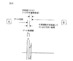
図2は、ソース電極8、ドレイン電極9、第1のゲート電極6の何れも接地状態の場合における図1中に示したA・B間のバンド構造を示した模式図である。なお、以後に図示する全ての多結晶シリコンのバンド構造は単純化のため、単結晶シリコンのバンド構造を用いている。
FIG. 2 is a schematic diagram showing the band structure between A and B shown in FIG. 1 when all of the
第1のゲート電極5と、P型の炭化珪素6中の、ヘテロ半導体領域3に対してビルトイン電界を及ぼす領域とに挟まれたヘテロ半導体領域3の一部が、上記ヘテロ半導体領域3に対してビルトイン電界を及ぼす領域からのビルトイン電界と、第1のゲート絶縁膜4を介した第1のゲート電極5からのビルトイン電界とによって、図2中に示したように空乏化する。この状態においては、ヘテロ半導体領域3がP型の炭化珪素6中の、ヘテロ半導体領域3に対してビルトイン電界を及ぼす領域からのビルトイン電界の影響によって空乏化した分、キャリアの通路が狭くなり、P型の炭化珪素6中の、ヘテロ半導体領域3に対してビルトイン電界を及ぼす領域が存在していない場合と比較すると、ソース電極8・ヘテロ接合間の抵抗が高くなっている。
A part of the
図2の状態から、第1のゲート電極5とP型の炭化珪素6中の、ヘテロ半導体領域3に対してビルトイン電界を及ぼす領域とに挟まれたヘテロ半導体領域3の幅を、第1のゲート絶縁膜4とヘテロ半導体領域3との接合界面からヘテロ半導体領域3へ伸びる第1のゲート電極5からの電界の及ぶ距離と、ヘテロ半導体領域3に対してビルトイン電界を及ぼす領域とヘテロ半導体領域3との接合界面からヘテロ半導体領域3へ伸びるP型の炭化珪素6中の、ヘテロ半導体領域3に対してビルトイン電界を及ぼす領域からの電界の及ぶ距離との和よりも小さくすると、バンド構造は図3に示すようになり、第1のゲート電極5とP型の炭化珪素6中の、ヘテロ半導体領域3に対してビルトイン電界を及ぼす領域とに挟まれたヘテロ半導体領域3は完全に空乏化した状態になる。この場合、ソース電極8・ヘテロ接合間は電気的に完全に遮断された状態になる。この状態における、図1中に示したC・D間のバンド構造は図4の(a)に示すようになる。
From the state of FIG. 2, the width of the
ここで、ソース電極8と第1のゲート電極5を接地にした状態で、ドレイン電極9に然るべき電圧を印加すると、ソース電極8・ドレイン電極9間はヘテロ接合の障壁30によって、電気的に遮断された状態であるため、ソース電極8・ドレイン電極9間に電流は流れない。すなわちオフ状態となる。第1のゲート電極5とヘテロ半導体領域3に対してビルトイン電界を及ぼす領域とに挟まれたヘテロ半導体領域3は、完全に空乏化し、ピンチオフ状態になる。そのため、ソース電極・ヘテロ接合間は電気的に遮断された状態になり、ソース電極・ドレイン電極間に高電圧が印加された場合のヘテロ接合からのリーク電流をさらに低減することができる。
Here, when an appropriate voltage is applied to the
次に、ソース電極8を接地、ドレイン電極9に然るべき電圧を印加した状態で、第1のゲート電極5に然るべき電圧を印加すると、第1のゲート絶縁膜4を介してヘテロ半導体領域3に印加されるゲート電界によって、ヘテロ接合の障壁30の高さが変化するとともに、ヘテロ半導体領域3内部に形成された空乏化領域には電子31が蓄積し、蓄積層が形成される。この状態における図1中に示したC・D間のバンド構造は図4の(b)に示すようになり、ドレイン電極9からの電界によりソース電極8からドレイン電極9へと電子31が流れる。すなわち、オンの状態になる。オン時には、絶縁型の第1のゲート電極5からの電界によって、空乏化したヘテロ半導体領域3に蓄積層が形成されて抵抗が下がるので、オン抵抗の増大を招くことなく、オフ時のリーク電流を低減できる。
Next, when an appropriate voltage is applied to the
次に、ソース電極8を接地、ドレイン電極9に然るべき電圧を印加した状態で、第1のゲート電極5を接地して第1のゲート電極5に印加しているゲート電圧を取り除くと、図1中に示したC・D間のバンド構造は図4の(a)の状態に戻り、オフ状態となる。
Next, when the
このように、本実施形態における半導体装置はスイッチング動作をする。 Thus, the semiconductor device in this embodiment performs a switching operation.
また、ソース電極8と第1のゲート電極5とを接地した状態で、ドレイン電極9に高電圧が印加されると、図1中に示したC・D間のバンド構造は図4の(c)に示すようになる。この場合、ヘテロ接合界面のヘテロ半導体領域3側に蓄積した電子31によって電界が終端されるため、ヘテロ半導体領域3には殆ど電界が及ばず、ヘテロ半導体領域3が先にブレークダウンすることはない。また、ここで、ヘテロ接合の障壁30高さによっては、ヘテロ接合界面のヘテロ半導体領域3側に蓄積した電子31がヘテロ接合の障壁30を乗り越える或いはトンネリングすることで炭化珪素エピタキシャル層2側に流れようとするが、ヘテロ半導体領域3内部に形成された空乏化領域によってソース電極8・ヘテロ接合間は電気的に遮断されているため、電子31は炭化珪素エピタキシャル層2側には流れない。すなわち、ソース電極8・ドレイン電極9間に高電圧が印加された場合においても、本実施形態における半導体装置は高い遮断性を有している。
When a high voltage is applied to the
さらにP型の炭化珪素6中の、ヘテロ半導体領域3に対してビルトイン電界を及ぼす領域は、ソース電極8・ドレイン電極9間に高電圧が印加された場合において、電界緩和層としても作用し、ヘテロ接合界面近傍のドレイン電界を緩和するという効果も併せ持つ。
Further, the region of the P-
なお、本実施形態における半導体装置は、オフ時にはソース電極8・ヘテロ接合間に高抵抗層が挿入された状態、或いはソース電極8・ヘテロ接合間が電気的に遮断された状態になっているが、オン時には前述のように第1のゲート電極5から第1のゲート絶縁膜4を介してヘテロ半導体領域3に印加されるゲート電界によって、空乏化領域に蓄積層が形成されるため、オン時は、ヘテロ半導体領域3に対してビルトイン電界を及ぼす領域が存在しない場合と同等の特性を実現できる。すなわち、低オン抵抗と高耐圧の両立を図ることができる。
In the semiconductor device according to the present embodiment, the high resistance layer is inserted between the
このように、ヘテロ半導体領域3に対して電界を及ぼす領域に、第2導電型の第1の半導体材料(この場合にはP型の炭化珪素)を用いると、効果的に電界がヘテロ半導体領域3に伸延するので、ヘテロ半導体領域3がより空乏化しやすくなり、ソース電極・ヘテロ接合間の遮断性が向上することに加えて、第2導電型の半導体から第1導電型の半導体基体側へも空乏層が効率良く伸長するので、ヘテロ接合に印加される電界を効果的に緩和することができる。
As described above, when the second conductive type first semiconductor material (in this case, P-type silicon carbide) is used for the region that exerts an electric field on the
本実施形態における半導体装置は、ヘテロ半導体領域3に対してビルトイン電界を及ぼす領域がP型の炭化珪素6の一部分に形成されている場合について説明したが、P型の炭化珪素6ではなく、第2のゲート絶縁膜と第2のゲート電極からなる絶縁型のゲート領域、或いは仕事関数が第1導電型の第1の半導体材料の仕事関数、第2の半導体材料の仕事関数のいずれよりも大きい金属で構成されていても同様の効果を得ることができる。以下、その実施の形態について説明する。
In the semiconductor device according to the present embodiment, the case where the region that exerts the built-in electric field on the
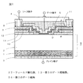
(第2の実施形態)
図5は本発明の第2の実施形態における半導体装置の断面図を示したものである。本実施形態においても、特許請求の範囲に記載の第1導電型はN型であり、第1の半導体材料は炭化珪素であり、第2の半導体材料は多結晶シリコンである。
(Second Embodiment)
FIG. 5 is a sectional view of a semiconductor device according to the second embodiment of the present invention. Also in the present embodiment, the first conductivity type described in the claims is N-type, the first semiconductor material is silicon carbide, and the second semiconductor material is polycrystalline silicon.
図5において、第1導電型であるN型の炭化珪素基板1と炭化珪素基板1より不純物濃度が低いN型の炭化珪素エピタキシャル層2とからなる、第1導電型の第1の半導体材料からなる半導体基体である炭化珪素半導体基体100と、炭化珪素半導体基体100とヘテロ接合する炭化珪素とはバンドギャップの異なる第2の半導体材料である多結晶シリコンからなるヘテロ半導体領域3と、炭化珪素エピタキシャル層2とヘテロ半導体領域3とによって形成されるヘテロ接合部に隣接して第1のゲート絶縁膜4を介して配設された第1のゲート電極5と、ヘテロ半導体領域3を介して第1のゲート電極5と対向するように配設され且つヘテロ半導体領域3に接触するように配設された、仕事関数がN型の炭化珪素の仕事関数、多結晶シリコンの仕事関数のいずれよりも大きい金属7と、ヘテロ半導体領域3に接触するソース電極8と、炭化珪素半導体基体100に接触するドレイン電極9とが形成されている。なお、半導体材料の仕事関数とは、電子親和力:χと伝導帯からフェルミレベルまでのエネルギー差:Ec−Efとの和を指している。
In FIG. 5, an N-type
金属7の、第1のゲート電極5と対向する部分が、ヘテロ半導体領域3に対してビルトイン電界を及ぼす領域となっており、この領域はヘテロ半導体領域3に接触している。すなわち、ヘテロ半導体領域3に対してビルトイン電界を及ぼす領域は、ヘテロ半導体領域3に接して配設され、N型の炭化珪素の仕事関数、多結晶シリコンの仕事関数のいずれよりも大きい仕事関数を有する金属7の、第1のゲート電極5と対向する部分からなり且つへテロ半導体領域3に接触している。
A portion of the
ソース電極8と第1のゲート電極5は層間絶縁膜11によって電気的に絶縁されている。また、図示はしていないが、仕事関数が炭化珪素より大きい金属7中の、ヘテロ半導体領域3に対してビルトイン電界を及ぼす領域は、図5の奥行き方向でソース電極8と接触している。
The
本実施形態における半導体装置は、図5中に示したA・B間のバンド構造は、図6に示すようになり、図3に示したP型の炭化珪素を用いた場合と同様にヘテロ半導体領域3は完全に空乏化した状態になる。そのため、図5中に示したC・D間のバンド構造は、図4の(a)と同様になり、本実施形態における半導体装置は、本発明の第1の実施形態における半導体装置と同様の素子特性を示す。
In the semiconductor device according to the present embodiment, the band structure between A and B shown in FIG. 5 is as shown in FIG. 6, and the hetero semiconductor is the same as in the case of using the P-type silicon carbide shown in FIG.
ここで、仕事関数がN型の炭化珪素の仕事関数、多結晶シリコンの仕事関数のいずれよりも大きい金属7に、たとえばニッケル(Ni)や白金(Pt)などを用いると、多結晶シリコンと金属との接合界面に形成されるショットキー障壁が高くなるため、効果的にヘテロ半導体領域3にビルトイン電界を伸長することができる。
Here, if, for example, nickel (Ni) or platinum (Pt) is used for the
(第3の実施形態)
図7は本発明の第3の実施形態における半導体装置の断面図を示したものである。本実施形態においても、特許請求の範囲に記載の第1導電型はN型であり、第1の半導体材料は炭化珪素であり、第2の半導体材料は多結晶シリコンである。
(Third embodiment)
FIG. 7 is a sectional view of a semiconductor device according to the third embodiment of the present invention. Also in the present embodiment, the first conductivity type described in the claims is N-type, the first semiconductor material is silicon carbide, and the second semiconductor material is polycrystalline silicon.
図7において、N型の炭化珪素基板1と炭化珪素基板1より不純物濃度が低いN型の炭化珪素エピタキシャル層2とからなる炭化珪素半導体基体100と、炭化珪素半導体基体100とヘテロ接合する炭化珪素とはバンドギャップの異なる第2の半導体材料である多結晶シリコンからなるヘテロ半導体領域3と、炭化珪素エピタキシャル層2とヘテロ半導体領域3とによって形成されるヘテロ接合部に隣接して第1のゲート絶縁膜4を介して配設された第1のゲート電極5と、ヘテロ半導体領域3を介して第1のゲート電極5と対向するように配設された第2のゲート絶縁膜13と第2のゲート電極14とからなる絶縁型のゲート領域と、ヘテロ半導体領域3に接触するソース電極8と、炭化珪素半導体基体100に接触するドレイン電極9とが形成されている。
In FIG. 7, a silicon
なお、第2のゲート絶縁膜13は厚いフィールド酸化膜12上に形成されている。ソース電極8とゲート電極5は層間絶縁膜11によって電気的に絶縁されている。また、図示はしていないが、絶縁型ゲート領域における第2のゲート電極14は、図7の奥行き方向でゲート電極5と接触している。
The second
ヘテロ半導体領域3に対してビルトイン電界を及ぼす領域は、第2のゲート絶縁膜13及び第2のゲート電極14の、第1のゲート電極5と対向する部分からなる。
A region that exerts a built-in electric field on the
本実施形態における半導体装置は、図7中に示したA・B間のバンド構造は、図8に示すようになり、図3に示したP型の炭化珪素を用いた場合と同様にヘテロ半導体領域3は完全に空乏化した状態になる。そのため、図7中に示したC・D間のバンド構造は、図4の(a)と同様になり、本実施形態における半導体装置は、本発明の第1の実施形態における半導体装置や本発明の第2の実施形態における半導体装置と同様の素子特性を示す。
In the semiconductor device of this embodiment, the band structure between A and B shown in FIG. 7 is as shown in FIG. 8, and the hetero semiconductor is the same as in the case of using P-type silicon carbide shown in FIG.
このように、第1のゲート絶縁膜4と第1のゲート電極5とからなる第1のゲート領域と、第2のゲート絶縁膜13と第2のゲート電極14はからなる第2のゲート領域とによってヘテロ半導体領域3を挟むことで、ヘテロ半導体領域3を効率良く空乏化できる。さらに、第2のゲート電極14は絶縁型のゲート電極であるため、オフ時には負の電圧を印加して、よりよく遮断性を向上することもできる。
Thus, the first gate region composed of the first
以上、これまでに説明してきた本発明の第1の実施形態、第2の実施形態及び第3の実施形態における半導体装置はプレーナ型構造であり、ヘテロ半導体領域3が多結晶シリコンからなるため、ゲート電極5とヘテロ半導体領域3に対してビルトイン電界を及ぼす領域とに挟まれたヘテロ半導体領域3の幅を、ゲート絶縁膜4とヘテロ半導体領域3との接合界面からヘテロ半導体領域3へ伸びるゲート電極5からの電界の及ぶ距離と、ヘテロ半導体領域3に対してビルトイン電界を及ぼす領域とヘテロ半導体領域3との接合界面からヘテロ半導体領域3へ伸びるヘテロ半導体領域3に対してビルトイン電界を及ぼす領域からの電界の及ぶ距離との和よりも小さくする、すなわち多結晶シリコンの厚さを薄くすることが容易であるという製造上のメリットも併せ持っている。
As described above, the semiconductor devices in the first embodiment, the second embodiment, and the third embodiment of the present invention described so far have a planar structure, and the
(第4の実施形態)
図9は本発明の第4の実施形態における半導体装置の断面図を示したものである。本実施形態においても、特許請求の範囲に記載の第1導電型はN型であり、第1の半導体材料は炭化珪素であり、第2の半導体材料は多結晶シリコンである。
(Fourth embodiment)
FIG. 9 is a sectional view of a semiconductor device according to the fourth embodiment of the present invention. Also in the present embodiment, the first conductivity type described in the claims is N-type, the first semiconductor material is silicon carbide, and the second semiconductor material is polycrystalline silicon.
図9において、N型の炭化珪素基板1と炭化珪素基板1より不純物濃度が低いN型の炭化珪素エピタキシャル層2とからなる炭化珪素半導体基体100と、炭化珪素半導体基体100とヘテロ接合する炭化珪素とはバンドギャップの異なる第2の半導体材料である多結晶シリコンからなるヘテロ半導体領域3と、ヘテロ半導体領域3を深さ方向に貫通して炭化珪素半導体基体100に達するように形成された溝10と、溝10内に形成され且つ炭化珪素エピタキシャル層2とヘテロ半導体領域3とによって形成されるヘテロ接合部に隣接してゲート絶縁膜4を介して配設されたゲート電極5と、ヘテロ半導体領域3を介してゲート電極5と対向するように配設され且つヘテロ半導体領域3に接触するように配設されたP型の炭化珪素6の一部分からなる、ヘテロ半導体領域3に対してビルトイン電界を及ぼす領域と、ヘテロ半導体領域3に接触するソース電極8と、炭化珪素半導体基体100に接触するドレイン電極9とが形成されている。
In FIG. 9, silicon
ソース電極8とゲート電極5は層間絶縁膜11によって電気的に絶縁されている。また、図示はしていないが、P型の炭化珪素6中の、ヘテロ半導体領域3に対してビルトイン電界を及ぼす領域は、図9の奥行き方向でソース電極8と接触している。
The
図9に示す半導体装置は、上記の効果に加えて、溝10内部にゲート絶縁膜4及びゲート電極5を形成したトレンチゲート構造になっているため、単一セルあたりの素子面積を小さくすることができる。すなわち高集積化を図ることができ、オン抵抗をより低減することができる。
In addition to the above effects, the semiconductor device shown in FIG. 9 has a trench gate structure in which the
なお、本実施形態における半導体装置においては、ヘテロ半導体領域3に対してビルトイン電界を及ぼす領域にP型の炭化珪素6の一部分を用いているが、このP型の炭化珪素6に代えて、本発明の第2の実施形態における半導体装置或いは第3の実施形態における半導体装置と同様に、第2のゲート絶縁膜13と第2のゲート電極14からなる絶縁型のゲート領域、或いは仕事関数がN型の炭化珪素の仕事関数、多結晶シリコンの仕事関数のいずれよりも大きい金属7を用いても同様の効果を得ることができる。
In the semiconductor device according to the present embodiment, a part of P-
上記の実施形態においては、第1の半導体材料として炭化珪素を用いているが、これにより、高耐圧な半導体装置を実現させることができる。 In the above embodiment, silicon carbide is used as the first semiconductor material, but this makes it possible to realize a semiconductor device with a high breakdown voltage.
また、上記の実施形態においては、第2の半導体材料として多結晶シリコンを用いているが、これにより、良好なヘテロ接合が形成できるので、上記記載の本発明の効果が得られやすい。 In the above-described embodiment, polycrystalline silicon is used as the second semiconductor material. However, this makes it possible to form a favorable heterojunction, so that the effects of the present invention described above can be easily obtained.
さらに、多結晶シリコンに代えて、単結晶シリコンまたはアモルファスシリコンを用いても、良好なヘテロ接合が形成できるので、上記記載の本発明の効果が得られやすい。すなわち、第2の半導体材料が、多結晶シリコン、単結晶シリコン、アモルファスシリコンのうちの少なくとも1つからなることによっても、本発明の効果が得られる。また、多結晶シリコン、単結晶シリコンまたはアモルファスシリコンにおいては、半導体基体上への堆積、酸化、パターニング、選択的エッチング、選択的伝導度制御等のプロセスが容易になり、好都合である。 Further, even when single crystal silicon or amorphous silicon is used in place of polycrystalline silicon, a good heterojunction can be formed, so that the effects of the present invention described above can be easily obtained. That is, the effect of the present invention can also be obtained when the second semiconductor material is made of at least one of polycrystalline silicon, single crystal silicon, and amorphous silicon. Polycrystalline silicon, single crystal silicon, or amorphous silicon is advantageous because it facilitates processes such as deposition on a semiconductor substrate, oxidation, patterning, selective etching, and selective conductivity control.
以上、説明してきた実施形態においては、第1の半導体材料を炭化珪素、第2の半導体材料を多結晶シリコンとした例で説明したが、半導体基体を構成する半導体材料及びヘテロ半導体領域を形成する半導体材料についてはこの限りではない。例えば、第1の半導体材料には、窒化ガリウムなどを用いてもよいし、第2の半導体材料にはシリコンゲルマニウムなどを用いてもよい。さらに、ここで用いられている炭化珪素(SiC)の結晶系は4Hが代表的であるが、6H、3C等その他の結晶系でも構わない。 In the embodiment described above, the example in which the first semiconductor material is silicon carbide and the second semiconductor material is polycrystalline silicon has been described. However, the semiconductor material constituting the semiconductor substrate and the hetero semiconductor region are formed. This does not apply to semiconductor materials. For example, gallium nitride or the like may be used for the first semiconductor material, and silicon germanium or the like may be used for the second semiconductor material. Further, the crystal system of silicon carbide (SiC) used here is typically 4H, but other crystal systems such as 6H and 3C may be used.
また、上記本発明の全ての実施形態において、ヘテロ半導体領域を構成する第2の半導体材料第1導電型であるN型の多結晶シリコンを用いた蓄積型の半導体装置について説明しているが、第2導電型であるP型の多結晶シリコンを用いた場合、すなわち反転型の半導体装置においても同様の効果を得ることができる。 Moreover, in all the embodiments of the present invention, the storage type semiconductor device using the N-type polycrystalline silicon which is the second semiconductor material first conductivity type constituting the hetero semiconductor region has been described. The same effect can be obtained even when P-type polycrystalline silicon, which is the second conductivity type, is used, that is, in an inversion type semiconductor device.
なお、上記実施形態においては第1導電型をN型、第2導電型をP型としているが、第1導電型をP型、第2導電型をN型とした場合においても同様の効果を得ることができる。 In the above embodiment, the first conductivity type is N-type and the second conductivity type is P-type. However, the same effect can be obtained when the first conductivity type is P-type and the second conductivity type is N-type. Obtainable.
さらには、本発明の主旨を逸脱しない範囲での変形を含むことは言うまでもない。 Furthermore, it goes without saying that modifications are included within the scope not departing from the gist of the present invention.
1…炭化珪素基板、2…炭化珪素エピタキシャル層、3…ヘテロ半導体領域、4…第1のゲート絶縁膜、5…第1のゲート電極、6…P型の炭化珪素、7…金属、8…ソース電極、9…ドレイン電極、10…溝、11…層間絶縁膜、12…フィールド酸化膜、13…第2のゲート絶縁膜、14…第2のゲート電極、30…障壁、31…電子、100…炭化珪素半導体基体。
DESCRIPTION OF
Claims (9)
前記第1のゲート絶縁膜及びヘテロ半導体領域を介して前記第1のゲート電極の少なくとも一部と対向する部位に前記ヘテロ半導体領域に対してビルトイン電界を及ぼす領域を有し、
前記ヘテロ半導体領域に対してビルトイン電界を及ぼす領域が、前記ヘテロ半導体領域に接して配設された第2のゲート絶縁膜及び該第2のゲート絶縁膜に接して配設された第2のゲート電極からなることを特徴とする半導体装置。 A semiconductor substrate made of a first semiconductor material of a first conductivity type, a hetero semiconductor region heterojunctioned with the semiconductor substrate and made of a second semiconductor material having a band gap different from that of the first semiconductor material, and the semiconductor substrate A first gate electrode disposed through a first gate insulating film adjacent to a junction between the hetero semiconductor region, a source electrode in contact with the hetero semiconductor region, and a contact with the semiconductor substrate In a semiconductor device having a drain electrode to be
Have a region on the built-in field to the hetero semiconductor region in a portion that faces at least a portion of said first gate electrode through the first gate insulating film and the hetero semiconductor region,
A second gate insulating film disposed in contact with the hetero semiconductor region, and a second gate disposed in contact with the second gate insulating film, wherein the region that exerts a built-in electric field on the hetero semiconductor region A semiconductor device comprising an electrode .
前記第1のゲート絶縁膜及びヘテロ半導体領域を介して前記第1のゲート電極の少なくとも一部と対向する部位に前記ヘテロ半導体領域に対してビルトイン電界を及ぼす領域を有し、 A region that exerts a built-in electric field on the hetero semiconductor region at a portion facing at least a part of the first gate electrode via the first gate insulating film and the hetero semiconductor region;
前記ヘテロ半導体領域に対してビルトイン電界を及ぼす領域が、前記ヘテロ半導体領域に接して配設され、前記第1導電型の第1の半導体材料の仕事関数、前記第2の半導体材料の仕事関数のいずれよりも大きい仕事関数を有する金属からなり且つ前記へテロ半導体領域に接触していることを特徴とする半導体装置。 A region that exerts a built-in electric field on the hetero semiconductor region is disposed in contact with the hetero semiconductor region, and the work function of the first semiconductor material of the first conductivity type and the work function of the second semiconductor material are A semiconductor device comprising a metal having a work function larger than any of the above and contacting the hetero semiconductor region.
前記第1のゲート絶縁膜及びヘテロ半導体領域を介して前記第1のゲート電極の少なくとも一部と対向する部位に前記ヘテロ半導体領域に対してビルトイン電界を及ぼす領域を有し、
前記ヘテロ半導体領域に対してビルトイン電界を及ぼす領域が、前記ヘテロ半導体領域に接して配設された第2導電型の前記第1の半導体材料からなり且つ前記へテロ半導体領域に接触していることを特徴とする半導体装置。 A semiconductor substrate made of a first semiconductor material of a first conductivity type, a hetero semiconductor region heterojunctioned with the semiconductor substrate and made of a second semiconductor material having a band gap different from that of the first semiconductor material, and the semiconductor substrate A first gate electrode disposed through a first gate insulating film adjacent to a junction between the hetero semiconductor region, a source electrode in contact with the hetero semiconductor region, and a contact with the semiconductor substrate In a semiconductor device having a drain electrode to be
A region that exerts a built-in electric field on the hetero semiconductor region at a portion facing at least a part of the first gate electrode via the first gate insulating film and the hetero semiconductor region;
The region that exerts a built-in electric field on the hetero semiconductor region is made of the first semiconductor material of the second conductivity type disposed in contact with the hetero semiconductor region and is in contact with the hetero semiconductor region. A semiconductor device characterized by the above.
前記第1のゲート絶縁膜及びヘテロ半導体領域を介して前記第1のゲート電極の少なくとも一部と対向する部位に前記ヘテロ半導体領域に対してビルトイン電界を及ぼす領域を有し、
前記ヘテロ半導体領域に対してビルトイン電界を及ぼす領域が、前記ヘテロ半導体領域に接して配設された第2のゲート絶縁膜及び該第2のゲート絶縁膜に接して配設された第2のゲート電極からなることを特徴とする半導体装置。 A semiconductor substrate made of a first semiconductor material of a first conductivity type, a hetero semiconductor region made of a second semiconductor material heterojunction with the semiconductor substrate and having a band gap different from that of the first semiconductor material, and the hetero semiconductor A trench formed so as to penetrate the region in the depth direction and reach the semiconductor substrate, a first gate electrode disposed in the trench via a first gate insulating film, and the hetero semiconductor region In a semiconductor device having a source electrode that contacts the drain electrode and a drain electrode that contacts the semiconductor substrate,
A region that exerts a built-in electric field on the hetero semiconductor region at a portion facing at least a part of the first gate electrode via the first gate insulating film and the hetero semiconductor region ;
A second gate insulating film disposed in contact with the hetero semiconductor region, and a second gate disposed in contact with the second gate insulating film, wherein the region that exerts a built-in electric field on the hetero semiconductor region A semiconductor device comprising an electrode .
前記第1のゲート絶縁膜及びヘテロ半導体領域を介して前記第1のゲート電極の少なくとも一部と対向する部位に前記ヘテロ半導体領域に対してビルトイン電界を及ぼす領域を有し、 A region that exerts a built-in electric field on the hetero semiconductor region at a portion facing at least a part of the first gate electrode via the first gate insulating film and the hetero semiconductor region;
前記ヘテロ半導体領域に対してビルトイン電界を及ぼす領域が、前記ヘテロ半導体領域に接して配設され、前記第1導電型の第1の半導体材料の仕事関数、前記第2の半導体材料の仕事関数のいずれよりも大きい仕事関数を有する金属からなり且つ前記へテロ半導体領域に接触していることを特徴とする半導体装置。 A region that exerts a built-in electric field on the hetero semiconductor region is disposed in contact with the hetero semiconductor region, and the work function of the first semiconductor material of the first conductivity type and the work function of the second semiconductor material are A semiconductor device comprising a metal having a work function larger than any of the above and contacting the hetero semiconductor region.
前記第1のゲート絶縁膜及びヘテロ半導体領域を介して前記第1のゲート電極の少なくとも一部と対向する部位に前記ヘテロ半導体領域に対してビルトイン電界を及ぼす領域を有し、 A region that exerts a built-in electric field on the hetero semiconductor region at a portion facing at least a part of the first gate electrode via the first gate insulating film and the hetero semiconductor region;
前記ヘテロ半導体領域に対してビルトイン電界を及ぼす領域が、前記ヘテロ半導体領域に接して配設された第2導電型の前記第1の半導体材料からなり且つ前記へテロ半導体領域に接触していることを特徴とする半導体装置。 The region that exerts a built-in electric field on the hetero semiconductor region is made of the first semiconductor material of the second conductivity type disposed in contact with the hetero semiconductor region and is in contact with the hetero semiconductor region. A semiconductor device characterized by the above.
Priority Applications (4)
| Application Number | Priority Date | Filing Date | Title |
|---|---|---|---|
| JP2004065474A JP4039376B2 (en) | 2004-03-09 | 2004-03-09 | Semiconductor device |
| US11/068,803 US7061027B2 (en) | 2004-03-09 | 2005-03-02 | Semiconductor device with heterojunction |
| EP20050004690 EP1575097B1 (en) | 2004-03-09 | 2005-03-03 | Semiconductor device with heterojunction |
| EP13181557.3A EP2672518B1 (en) | 2004-03-09 | 2005-03-03 | Semiconductor device with heterojunction |
Applications Claiming Priority (1)
| Application Number | Priority Date | Filing Date | Title |
|---|---|---|---|
| JP2004065474A JP4039376B2 (en) | 2004-03-09 | 2004-03-09 | Semiconductor device |
Publications (2)
| Publication Number | Publication Date |
|---|---|
| JP2005259766A JP2005259766A (en) | 2005-09-22 |
| JP4039376B2 true JP4039376B2 (en) | 2008-01-30 |
Family
ID=34824551
Family Applications (1)
| Application Number | Title | Priority Date | Filing Date |
|---|---|---|---|
| JP2004065474A Expired - Lifetime JP4039376B2 (en) | 2004-03-09 | 2004-03-09 | Semiconductor device |
Country Status (3)
| Country | Link |
|---|---|
| US (1) | US7061027B2 (en) |
| EP (2) | EP2672518B1 (en) |
| JP (1) | JP4039376B2 (en) |
Families Citing this family (18)
| Publication number | Priority date | Publication date | Assignee | Title |
|---|---|---|---|---|
| JP4018641B2 (en) | 2002-04-12 | 2007-12-05 | ナショナル・ペイントボール・サプライ・インコーポレイテッド | A difference detection system for controlling the feed of a paintball loader |
| US7282739B2 (en) * | 2002-04-26 | 2007-10-16 | Nissan Motor Co., Ltd. | Silicon carbide semiconductor device |
| US7355207B2 (en) * | 2004-05-24 | 2008-04-08 | Denso Corporation | Silicon carbide semiconductor device and method for manufacturing the same |
| JP5087818B2 (en) * | 2005-03-25 | 2012-12-05 | 日亜化学工業株式会社 | Field effect transistor |
| JP5017877B2 (en) * | 2006-02-09 | 2012-09-05 | 日産自動車株式会社 | Semiconductor device |
| US7714352B2 (en) * | 2006-02-09 | 2010-05-11 | Nissan Motor Co., Ltd. | Hetero junction semiconductor device |
| JP2007234942A (en) * | 2006-03-02 | 2007-09-13 | Nissan Motor Co Ltd | Method of manufacturing semiconductor device |
| JP5034278B2 (en) * | 2006-03-10 | 2012-09-26 | 日産自動車株式会社 | Manufacturing method of semiconductor device |
| EP1850396A3 (en) * | 2006-04-28 | 2008-09-17 | Nissan Motor Co., Ltd. | Semiconductor device and manufacturing method thereof |
| JP5055945B2 (en) * | 2006-10-18 | 2012-10-24 | 日産自動車株式会社 | Semiconductor device and manufacturing method of semiconductor device |
| US8067776B2 (en) * | 2007-06-08 | 2011-11-29 | Nissan Motor Co., Ltd. | Method of manufacturing semiconductor device and semiconductor device manufactured thereof |
| US7825465B2 (en) * | 2007-12-13 | 2010-11-02 | Fairchild Semiconductor Corporation | Structure and method for forming field effect transistor with low resistance channel region |
| FR2934716B1 (en) * | 2008-07-31 | 2010-09-10 | Commissariat Energie Atomique | SEMICONDUCTOR MATERIAL ELECTROLUMINESCENT DIODE AND MANUFACTURING METHOD THEREOF |
| JP5588670B2 (en) * | 2008-12-25 | 2014-09-10 | ローム株式会社 | Semiconductor device |
| JP5588671B2 (en) | 2008-12-25 | 2014-09-10 | ローム株式会社 | Manufacturing method of semiconductor device |
| JP2011134910A (en) | 2009-12-24 | 2011-07-07 | Rohm Co Ltd | Sic field effect transistor |
| CN109119463B (en) * | 2018-08-29 | 2020-07-31 | 电子科技大学 | Transverse groove type MOSFET device and preparation method thereof |
| JP6969586B2 (en) * | 2019-04-23 | 2021-11-24 | 株式会社デンソー | Semiconductor devices and their manufacturing methods |
Family Cites Families (15)
| Publication number | Priority date | Publication date | Assignee | Title |
|---|---|---|---|---|
| US5396085A (en) * | 1993-12-28 | 1995-03-07 | North Carolina State University | Silicon carbide switching device with rectifying-gate |
| US5581100A (en) * | 1994-08-30 | 1996-12-03 | International Rectifier Corporation | Trench depletion MOSFET |
| JPH08204179A (en) * | 1995-01-26 | 1996-08-09 | Fuji Electric Co Ltd | Silicon carbide trench mosfet |
| US5895951A (en) * | 1996-04-05 | 1999-04-20 | Megamos Corporation | MOSFET structure and fabrication process implemented by forming deep and narrow doping regions through doping trenches |
| US5923051A (en) * | 1996-04-24 | 1999-07-13 | Abb Research Ltd. | Field controlled semiconductor device of SiC and a method for production thereof |
| US5719409A (en) * | 1996-06-06 | 1998-02-17 | Cree Research, Inc. | Silicon carbide metal-insulator semiconductor field effect transistor |
| JP3461274B2 (en) * | 1996-10-16 | 2003-10-27 | 株式会社東芝 | Semiconductor device |
| US6194741B1 (en) * | 1998-11-03 | 2001-02-27 | International Rectifier Corp. | MOSgated trench type power semiconductor with silicon carbide substrate and increased gate breakdown voltage and reduced on-resistance |
| JP2003533889A (en) * | 2000-05-13 | 2003-11-11 | コーニンクレッカ フィリップス エレクトロニクス エヌ ヴィ | Trench gate semiconductor device |
| US6552363B2 (en) * | 2001-09-18 | 2003-04-22 | International Rectifier Corporation | Polysilicon FET built on silicon carbide diode substrate |
| JP2003218398A (en) | 2002-01-18 | 2003-07-31 | Citizen Electronics Co Ltd | Surface mount type light emitting diode and its manufacturing method |
| US7282739B2 (en) * | 2002-04-26 | 2007-10-16 | Nissan Motor Co., Ltd. | Silicon carbide semiconductor device |
| JP3620513B2 (en) * | 2002-04-26 | 2005-02-16 | 日産自動車株式会社 | Silicon carbide semiconductor device |
| US7217950B2 (en) * | 2002-10-11 | 2007-05-15 | Nissan Motor Co., Ltd. | Insulated gate tunnel-injection device having heterojunction and method for manufacturing the same |
| JP4066946B2 (en) * | 2003-12-18 | 2008-03-26 | 日産自動車株式会社 | Semiconductor device |
-
2004
- 2004-03-09 JP JP2004065474A patent/JP4039376B2/en not_active Expired - Lifetime
-
2005
- 2005-03-02 US US11/068,803 patent/US7061027B2/en active Active
- 2005-03-03 EP EP13181557.3A patent/EP2672518B1/en active Active
- 2005-03-03 EP EP20050004690 patent/EP1575097B1/en active Active
Also Published As
| Publication number | Publication date |
|---|---|
| EP1575097A3 (en) | 2010-01-20 |
| EP2672518B1 (en) | 2021-05-05 |
| EP2672518A3 (en) | 2014-01-22 |
| US20050199873A1 (en) | 2005-09-15 |
| US7061027B2 (en) | 2006-06-13 |
| EP2672518A2 (en) | 2013-12-11 |
| EP1575097A2 (en) | 2005-09-14 |
| EP1575097B1 (en) | 2015-05-06 |
| JP2005259766A (en) | 2005-09-22 |
Similar Documents
| Publication | Publication Date | Title |
|---|---|---|
| JP4900662B2 (en) | Silicon carbide MOS field effect transistor with built-in Schottky diode and manufacturing method thereof | |
| JP4039376B2 (en) | Semiconductor device | |
| JP5940235B1 (en) | Semiconductor device | |
| JP5992094B2 (en) | Semiconductor device | |
| JP4066946B2 (en) | Semiconductor device | |
| JP3620513B2 (en) | Silicon carbide semiconductor device | |
| US8217419B2 (en) | Semiconductor device | |
| JP2007013058A (en) | Semiconductor device | |
| JP2005011846A (en) | Semiconductor device | |
| JP2017069551A (en) | Semiconductor element | |
| JP2018022852A (en) | Semiconductor device and manufacturing method of the same | |
| JP3826828B2 (en) | Field effect transistor using silicon carbide semiconductor | |
| CN112447857A (en) | Silicon carbide field effect transistor | |
| JP4948784B2 (en) | Semiconductor device and manufacturing method thereof | |
| JP4742539B2 (en) | Semiconductor device | |
| JP5092244B2 (en) | Semiconductor device | |
| JP5098293B2 (en) | Insulated gate type semiconductor device using wide band gap semiconductor and manufacturing method thereof | |
| JP4131193B2 (en) | Semiconductor device | |
| JP3975992B2 (en) | Semiconductor device and manufacturing method thereof | |
| JP2023500880A (en) | Vertical field effect transistor and method for its formation | |
| JP4687041B2 (en) | Manufacturing method of semiconductor device | |
| JPH09246545A (en) | Semiconductor element for power | |
| JP2006086397A (en) | Semiconductor device and its manufacturing method | |
| JP7411465B2 (en) | semiconductor equipment | |
| JP2006093545A (en) | Semiconductor device |
Legal Events
| Date | Code | Title | Description |
|---|---|---|---|
| A977 | Report on retrieval |
Free format text: JAPANESE INTERMEDIATE CODE: A971007 Effective date: 20070626 |
|
| A131 | Notification of reasons for refusal |
Free format text: JAPANESE INTERMEDIATE CODE: A131 Effective date: 20070703 |
|
| A521 | Written amendment |
Free format text: JAPANESE INTERMEDIATE CODE: A523 Effective date: 20070831 |
|
| A521 | Written amendment |
Free format text: JAPANESE INTERMEDIATE CODE: A523 Effective date: 20070912 |
|
| TRDD | Decision of grant or rejection written | ||
| A01 | Written decision to grant a patent or to grant a registration (utility model) |
Free format text: JAPANESE INTERMEDIATE CODE: A01 Effective date: 20071016 |
|
| A61 | First payment of annual fees (during grant procedure) |
Free format text: JAPANESE INTERMEDIATE CODE: A61 Effective date: 20071029 |
|
| FPAY | Renewal fee payment (event date is renewal date of database) |
Free format text: PAYMENT UNTIL: 20101116 Year of fee payment: 3 |
|
| R150 | Certificate of patent or registration of utility model |
Free format text: JAPANESE INTERMEDIATE CODE: R150 Ref document number: 4039376 Country of ref document: JP Free format text: JAPANESE INTERMEDIATE CODE: R150 |
|
| FPAY | Renewal fee payment (event date is renewal date of database) |
Free format text: PAYMENT UNTIL: 20111116 Year of fee payment: 4 |
|
| FPAY | Renewal fee payment (event date is renewal date of database) |
Free format text: PAYMENT UNTIL: 20121116 Year of fee payment: 5 |
|
| FPAY | Renewal fee payment (event date is renewal date of database) |
Free format text: PAYMENT UNTIL: 20121116 Year of fee payment: 5 |
|
| FPAY | Renewal fee payment (event date is renewal date of database) |
Free format text: PAYMENT UNTIL: 20131116 Year of fee payment: 6 |