JP6779211B2 - 基材導波光学装置 - Google Patents
基材導波光学装置 Download PDFInfo
- Publication number
- JP6779211B2 JP6779211B2 JP2017534237A JP2017534237A JP6779211B2 JP 6779211 B2 JP6779211 B2 JP 6779211B2 JP 2017534237 A JP2017534237 A JP 2017534237A JP 2017534237 A JP2017534237 A JP 2017534237A JP 6779211 B2 JP6779211 B2 JP 6779211B2
- Authority
- JP
- Japan
- Prior art keywords
- substrate
- loe
- base material
- light
- optical
- Prior art date
- Legal status (The legal status is an assumption and is not a legal conclusion. Google has not performed a legal analysis and makes no representation as to the accuracy of the status listed.)
- Active
Links
- 239000000758 substrate Substances 0.000 title claims description 54
- 230000003287 optical effect Effects 0.000 title claims description 50
- 239000000463 material Substances 0.000 claims description 29
- 238000000576 coating method Methods 0.000 claims description 20
- 239000011248 coating agent Substances 0.000 claims description 19
- 238000012546 transfer Methods 0.000 claims description 6
- 230000008878 coupling Effects 0.000 claims 2
- 238000010168 coupling process Methods 0.000 claims 2
- 238000005859 coupling reaction Methods 0.000 claims 2
- 238000000034 method Methods 0.000 description 9
- 239000010410 layer Substances 0.000 description 7
- 239000000853 adhesive Substances 0.000 description 6
- 230000001070 adhesive effect Effects 0.000 description 6
- 230000003667 anti-reflective effect Effects 0.000 description 3
- 238000010586 diagram Methods 0.000 description 3
- 239000012790 adhesive layer Substances 0.000 description 2
- 230000004075 alteration Effects 0.000 description 2
- 238000013459 approach Methods 0.000 description 2
- 238000012937 correction Methods 0.000 description 2
- 239000003989 dielectric material Substances 0.000 description 2
- 230000009977 dual effect Effects 0.000 description 2
- 238000003384 imaging method Methods 0.000 description 2
- 230000010287 polarization Effects 0.000 description 2
- 239000007787 solid Substances 0.000 description 2
- 238000001228 spectrum Methods 0.000 description 2
- 239000010409 thin film Substances 0.000 description 2
- 201000009310 astigmatism Diseases 0.000 description 1
- 230000008021 deposition Effects 0.000 description 1
- 238000011161 development Methods 0.000 description 1
- 238000005516 engineering process Methods 0.000 description 1
- 230000004424 eye movement Effects 0.000 description 1
- 239000004973 liquid crystal related substance Substances 0.000 description 1
- 239000002184 metal Substances 0.000 description 1
- 239000002991 molded plastic Substances 0.000 description 1
- 208000001491 myopia Diseases 0.000 description 1
- 230000004379 myopia Effects 0.000 description 1
- ORQBXQOJMQIAOY-UHFFFAOYSA-N nobelium Chemical compound [No] ORQBXQOJMQIAOY-UHFFFAOYSA-N 0.000 description 1
- 239000013307 optical fiber Substances 0.000 description 1
- 230000000644 propagated effect Effects 0.000 description 1
- 230000001681 protective effect Effects 0.000 description 1
- 210000001747 pupil Anatomy 0.000 description 1
- 230000001179 pupillary effect Effects 0.000 description 1
- 238000005482 strain hardening Methods 0.000 description 1
- 239000012780 transparent material Substances 0.000 description 1
Images


Classifications
-
- G—PHYSICS
- G02—OPTICS
- G02B—OPTICAL ELEMENTS, SYSTEMS OR APPARATUS
- G02B27/00—Optical systems or apparatus not provided for by any of the groups G02B1/00 - G02B26/00, G02B30/00
- G02B27/01—Head-up displays
- G02B27/0101—Head-up displays characterised by optical features
-
- G—PHYSICS
- G02—OPTICS
- G02B—OPTICAL ELEMENTS, SYSTEMS OR APPARATUS
- G02B27/00—Optical systems or apparatus not provided for by any of the groups G02B1/00 - G02B26/00, G02B30/00
- G02B27/0081—Optical systems or apparatus not provided for by any of the groups G02B1/00 - G02B26/00, G02B30/00 with means for altering, e.g. enlarging, the entrance or exit pupil
-
- G—PHYSICS
- G02—OPTICS
- G02B—OPTICAL ELEMENTS, SYSTEMS OR APPARATUS
- G02B27/00—Optical systems or apparatus not provided for by any of the groups G02B1/00 - G02B26/00, G02B30/00
- G02B27/01—Head-up displays
-
- G—PHYSICS
- G02—OPTICS
- G02B—OPTICAL ELEMENTS, SYSTEMS OR APPARATUS
- G02B27/00—Optical systems or apparatus not provided for by any of the groups G02B1/00 - G02B26/00, G02B30/00
- G02B27/01—Head-up displays
- G02B27/017—Head mounted
- G02B27/0172—Head mounted characterised by optical features
-
- G—PHYSICS
- G02—OPTICS
- G02B—OPTICAL ELEMENTS, SYSTEMS OR APPARATUS
- G02B27/00—Optical systems or apparatus not provided for by any of the groups G02B1/00 - G02B26/00, G02B30/00
- G02B27/01—Head-up displays
- G02B27/017—Head mounted
- G02B27/0176—Head mounted characterised by mechanical features
-
- G—PHYSICS
- G02—OPTICS
- G02B—OPTICAL ELEMENTS, SYSTEMS OR APPARATUS
- G02B27/00—Optical systems or apparatus not provided for by any of the groups G02B1/00 - G02B26/00, G02B30/00
- G02B27/10—Beam splitting or combining systems
- G02B27/14—Beam splitting or combining systems operating by reflection only
-
- G—PHYSICS
- G02—OPTICS
- G02B—OPTICAL ELEMENTS, SYSTEMS OR APPARATUS
- G02B27/00—Optical systems or apparatus not provided for by any of the groups G02B1/00 - G02B26/00, G02B30/00
- G02B27/42—Diffraction optics, i.e. systems including a diffractive element being designed for providing a diffractive effect
- G02B27/4205—Diffraction optics, i.e. systems including a diffractive element being designed for providing a diffractive effect having a diffractive optical element [DOE] contributing to image formation, e.g. whereby modulation transfer function MTF or optical aberrations are relevant
-
- G—PHYSICS
- G02—OPTICS
- G02B—OPTICAL ELEMENTS, SYSTEMS OR APPARATUS
- G02B6/00—Light guides; Structural details of arrangements comprising light guides and other optical elements, e.g. couplings
- G02B6/0001—Light guides; Structural details of arrangements comprising light guides and other optical elements, e.g. couplings specially adapted for lighting devices or systems
- G02B6/0011—Light guides; Structural details of arrangements comprising light guides and other optical elements, e.g. couplings specially adapted for lighting devices or systems the light guides being planar or of plate-like form
- G02B6/0013—Means for improving the coupling-in of light from the light source into the light guide
- G02B6/0023—Means for improving the coupling-in of light from the light source into the light guide provided by one optical element, or plurality thereof, placed between the light guide and the light source, or around the light source
- G02B6/0031—Reflecting element, sheet or layer
-
- G—PHYSICS
- G02—OPTICS
- G02B—OPTICAL ELEMENTS, SYSTEMS OR APPARATUS
- G02B6/00—Light guides; Structural details of arrangements comprising light guides and other optical elements, e.g. couplings
- G02B6/0001—Light guides; Structural details of arrangements comprising light guides and other optical elements, e.g. couplings specially adapted for lighting devices or systems
- G02B6/0011—Light guides; Structural details of arrangements comprising light guides and other optical elements, e.g. couplings specially adapted for lighting devices or systems the light guides being planar or of plate-like form
- G02B6/0033—Means for improving the coupling-out of light from the light guide
- G02B6/0035—Means for improving the coupling-out of light from the light guide provided on the surface of the light guide or in the bulk of it
-
- G—PHYSICS
- G02—OPTICS
- G02B—OPTICAL ELEMENTS, SYSTEMS OR APPARATUS
- G02B6/00—Light guides; Structural details of arrangements comprising light guides and other optical elements, e.g. couplings
- G02B6/0001—Light guides; Structural details of arrangements comprising light guides and other optical elements, e.g. couplings specially adapted for lighting devices or systems
- G02B6/0011—Light guides; Structural details of arrangements comprising light guides and other optical elements, e.g. couplings specially adapted for lighting devices or systems the light guides being planar or of plate-like form
- G02B6/0033—Means for improving the coupling-out of light from the light guide
- G02B6/005—Means for improving the coupling-out of light from the light guide provided by one optical element, or plurality thereof, placed on the light output side of the light guide
-
- G—PHYSICS
- G02—OPTICS
- G02B—OPTICAL ELEMENTS, SYSTEMS OR APPARATUS
- G02B6/00—Light guides; Structural details of arrangements comprising light guides and other optical elements, e.g. couplings
- G02B6/0001—Light guides; Structural details of arrangements comprising light guides and other optical elements, e.g. couplings specially adapted for lighting devices or systems
- G02B6/0011—Light guides; Structural details of arrangements comprising light guides and other optical elements, e.g. couplings specially adapted for lighting devices or systems the light guides being planar or of plate-like form
- G02B6/0065—Manufacturing aspects; Material aspects
-
- G—PHYSICS
- G02—OPTICS
- G02B—OPTICAL ELEMENTS, SYSTEMS OR APPARATUS
- G02B1/00—Optical elements characterised by the material of which they are made; Optical coatings for optical elements
- G02B1/10—Optical coatings produced by application to, or surface treatment of, optical elements
- G02B1/11—Anti-reflection coatings
-
- G—PHYSICS
- G02—OPTICS
- G02B—OPTICAL ELEMENTS, SYSTEMS OR APPARATUS
- G02B27/00—Optical systems or apparatus not provided for by any of the groups G02B1/00 - G02B26/00, G02B30/00
- G02B27/01—Head-up displays
- G02B27/0101—Head-up displays characterised by optical features
- G02B2027/0123—Head-up displays characterised by optical features comprising devices increasing the field of view
- G02B2027/0125—Field-of-view increase by wavefront division
-
- G—PHYSICS
- G02—OPTICS
- G02B—OPTICAL ELEMENTS, SYSTEMS OR APPARATUS
- G02B27/00—Optical systems or apparatus not provided for by any of the groups G02B1/00 - G02B26/00, G02B30/00
- G02B27/01—Head-up displays
- G02B27/0149—Head-up displays characterised by mechanical features
- G02B2027/015—Head-up displays characterised by mechanical features involving arrangement aiming to get less bulky devices
-
- G—PHYSICS
- G02—OPTICS
- G02B—OPTICAL ELEMENTS, SYSTEMS OR APPARATUS
- G02B27/00—Optical systems or apparatus not provided for by any of the groups G02B1/00 - G02B26/00, G02B30/00
- G02B27/01—Head-up displays
- G02B27/017—Head mounted
- G02B2027/0178—Eyeglass type
-
- G—PHYSICS
- G02—OPTICS
- G02B—OPTICAL ELEMENTS, SYSTEMS OR APPARATUS
- G02B6/00—Light guides; Structural details of arrangements comprising light guides and other optical elements, e.g. couplings
- G02B6/0001—Light guides; Structural details of arrangements comprising light guides and other optical elements, e.g. couplings specially adapted for lighting devices or systems
- G02B6/0011—Light guides; Structural details of arrangements comprising light guides and other optical elements, e.g. couplings specially adapted for lighting devices or systems the light guides being planar or of plate-like form
- G02B6/0013—Means for improving the coupling-in of light from the light source into the light guide
- G02B6/0015—Means for improving the coupling-in of light from the light source into the light guide provided on the surface of the light guide or in the bulk of it
Description
[外1]

a) 実線は、非接合、すなわち、外部の物質が空気であり、その外表面が共通の反射防止(AR)被覆を用いて被覆されているLOEの反射率曲線を表す。図示されているように、臨界角は38.7°であり、その値よりも下では、反射率は急速に低下する。
b) 点線は、1.1の屈折率を有するLIMの基材に接合されており、インターフェイス面は共通のAR被覆を用いて被覆されているLOEの反射率曲線を表示する。ここで、臨界角は43.4°に増大される。LOEの中に結合され得る潜在的なFOVは減少するが、それは、依然として合理的であり、臨界角が41.8°であるBK7で作製された非接合LOEと類似している。
c) 破線は、1.1の屈折率を有するLIMの基材に接合されたLOEの反射率曲線を表す。しかしながら、インターフェイス面は、ここで、特別なASR被覆を用いて被覆されている。43.4°よりも低い入射角度における、インターフェイス面からのLOEの内側の捕捉された光線の反射の光学配置は、もはや全内部反射ではなく、むしろASRからの被覆である。34.7°よりも高い入射角度でインターフェイス面に突き当たる光線の反射率は、99%よりも高く、光線は、インターフェイス面からほとんど全反射される。一つの結果として、このLOEの内側に捕捉され得る潜在的なFOVは、グラフ(a)に示される非接合LOEのそれよりもかなり高い。
Claims (2)
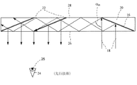
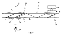
- 光学システムであって、
少なくとも二つの外部の主要面(26,28)及び端を有する、光伝達基材(20)、
全内部反射によって前記基材の中に光波を結合させるための、光学素子(16,102)、
前記基材の外に光波を結合させるための、前記基材(20)内に位置する少なくとも一つの部分反射面(22,104)、及び
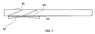
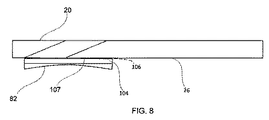
前記基材の前記主要面のうちの少なくとも一つに光学的に取り付けられており、インターフェイス平面を規定する、少なくとも一つの透明層(100,104,108)、
を有し、
前記少なくとも一つの透明層(100,104,108)は、臨界角よりも大きな角度で前記基材(20)の内側に結合された光波が、前記インターフェイス平面から、前記基材の前記主要面と前記透明層との間で、全内部反射によって前記基材の中に捕捉されるような臨界角を規定するように、前記光伝達基材の屈折率よりも低い屈折率を有し、
反射防止被覆が前記インターフェイス平面に塗布されている、光学システム。 - 光学システムであって、
少なくとも二つの外部の主要面(26,28)及び端を有する、光伝達基材(20)、
全内部反射によって前記基材の中に光波を結合させるための、光学素子(16,102)、
前記基材の外に光波を結合させるための、前記基材(20)内に位置する少なくとも一つの部分反射面(22,104)、及び
前記基材の前記主要面のうちの少なくとも一つに光学的に取り付けられており、インターフェイス平面を規定する、少なくとも一つの透明層(100,104,108)、
を有し、
前記少なくとも一つの透明層(100,104,108)は、臨界角よりも大きな角度で前記基材(20)の内側に結合された光波が、前記インターフェイス平面から、前記基材の前記主要面と前記透明層との間で、全内部反射によって前記基材の中に捕捉されるような臨界角を規定するように、前記光伝達基材の屈折率よりも低い屈折率を有し、
角度選択的反射被覆が前記インターフェイス平面に塗布されている、光学システム。
Priority Applications (2)
| Application Number | Priority Date | Filing Date | Title |
|---|---|---|---|
| JP2020030352A JP6966104B2 (ja) | 2014-12-25 | 2020-02-26 | 基材導波光学装置 |
| JP2021168461A JP2022009123A (ja) | 2014-12-25 | 2021-10-14 | 基材導波光学装置 |
Applications Claiming Priority (3)
| Application Number | Priority Date | Filing Date | Title |
|---|---|---|---|
| IL236490 | 2014-12-25 | ||
| IL236490A IL236490B (en) | 2014-12-25 | 2014-12-25 | Optical component on a conductive substrate |
| PCT/IL2015/051222 WO2016103251A1 (en) | 2014-12-25 | 2015-12-16 | Substrate-guided optical device |
Related Child Applications (1)
| Application Number | Title | Priority Date | Filing Date |
|---|---|---|---|
| JP2020030352A Division JP6966104B2 (ja) | 2014-12-25 | 2020-02-26 | 基材導波光学装置 |
Publications (3)
| Publication Number | Publication Date |
|---|---|
| JP2018503865A JP2018503865A (ja) | 2018-02-08 |
| JP2018503865A5 JP2018503865A5 (ja) | 2019-01-17 |
| JP6779211B2 true JP6779211B2 (ja) | 2020-11-04 |
Family
ID=54347971
Family Applications (3)
| Application Number | Title | Priority Date | Filing Date |
|---|---|---|---|
| JP2017534237A Active JP6779211B2 (ja) | 2014-12-25 | 2015-12-16 | 基材導波光学装置 |
| JP2020030352A Active JP6966104B2 (ja) | 2014-12-25 | 2020-02-26 | 基材導波光学装置 |
| JP2021168461A Pending JP2022009123A (ja) | 2014-12-25 | 2021-10-14 | 基材導波光学装置 |
Family Applications After (2)
| Application Number | Title | Priority Date | Filing Date |
|---|---|---|---|
| JP2020030352A Active JP6966104B2 (ja) | 2014-12-25 | 2020-02-26 | 基材導波光学装置 |
| JP2021168461A Pending JP2022009123A (ja) | 2014-12-25 | 2021-10-14 | 基材導波光学装置 |
Country Status (11)
| Country | Link |
|---|---|
| US (3) | US20180067315A1 (ja) |
| EP (2) | EP3237954A1 (ja) |
| JP (3) | JP6779211B2 (ja) |
| KR (2) | KR102292535B1 (ja) |
| CN (2) | CN111240019B (ja) |
| BR (1) | BR112017013680B1 (ja) |
| CA (1) | CA2969822C (ja) |
| IL (1) | IL236490B (ja) |
| RU (1) | RU2721661C2 (ja) |
| SG (2) | SG11201704276TA (ja) |
| WO (1) | WO2016103251A1 (ja) |
Families Citing this family (74)
| Publication number | Priority date | Publication date | Assignee | Title |
|---|---|---|---|---|
| IL166799A (en) | 2005-02-10 | 2014-09-30 | Lumus Ltd | Aluminum shale surfaces for use in a conductive substrate |
| US10073264B2 (en) | 2007-08-03 | 2018-09-11 | Lumus Ltd. | Substrate-guide optical device |
| US10048499B2 (en) | 2005-11-08 | 2018-08-14 | Lumus Ltd. | Polarizing optical system |
| IL219907A (en) | 2012-05-21 | 2017-08-31 | Lumus Ltd | Integrated head display system with eye tracking |
| IL232197B (en) | 2014-04-23 | 2018-04-30 | Lumus Ltd | Compact head-up display system |
| IL235642B (en) | 2014-11-11 | 2021-08-31 | Lumus Ltd | A compact head-up display system is protected by an element with a super-thin structure |
| IL237337B (en) | 2015-02-19 | 2020-03-31 | Amitai Yaakov | A compact head-up display system with a uniform image |
| DE102016105060B3 (de) * | 2016-03-18 | 2017-07-06 | Carl Zeiss Smart Optics Gmbh | Brillenglas für eine Abbildungsoptik, Abbildungsoptik und Datenbrille |
| US10133070B2 (en) | 2016-10-09 | 2018-11-20 | Lumus Ltd. | Aperture multiplier using a rectangular waveguide |
| JP6829482B2 (ja) * | 2016-11-08 | 2021-02-10 | ルムス エルティーディー. | 光学遮断端部を備えた光ガイド装置およびその製造方法 |
| WO2018138714A1 (en) * | 2017-01-28 | 2018-08-02 | Lumus Ltd. | Augmented reality imaging system |
| TWI754010B (zh) | 2017-02-22 | 2022-02-01 | 以色列商魯姆斯有限公司 | 導光光學組件 |
| KR20180106624A (ko) * | 2017-03-21 | 2018-10-01 | 주식회사 파노비젼 | 수평 및 수직 출사동 확장수단을 갖는 투과형 hmd 광학계 |
| KR20230025946A (ko) | 2017-03-22 | 2023-02-23 | 루머스 리미티드 | 중첩 파셋 |
| IL251645B (en) | 2017-04-06 | 2018-08-30 | Lumus Ltd | Waveguide and method of production |
| US20200183079A1 (en) * | 2017-05-19 | 2020-06-11 | Seereal Technologies S.A. | Display device comprising a light guide |
| TWI770234B (zh) | 2017-07-19 | 2022-07-11 | 以色列商魯姆斯有限公司 | 通過光導光學元件的矽基液晶照明器 |
| US11513352B2 (en) | 2017-09-29 | 2022-11-29 | Lumus Ltd. | Augmented reality display |
| CN115826239A (zh) * | 2017-10-16 | 2023-03-21 | 奥里姆光学有限公司 | 高效紧凑型头戴式显示系统 |
| JP7228584B2 (ja) | 2017-10-22 | 2023-02-24 | ラマス リミテッド | 光学ベンチを用いるヘッドマウント拡張現実デバイス |
| MX2020005226A (es) | 2017-11-21 | 2020-08-24 | Lumus Ltd | Dispositivo de expansion de apertura optica para pantallas de vision directa. |
| IL275013B (en) | 2017-12-03 | 2022-08-01 | Lumus Ltd | Method and device for testing an optics device |
| US11762169B2 (en) | 2017-12-03 | 2023-09-19 | Lumus Ltd. | Optical device alignment methods |
| CN107966819A (zh) * | 2017-12-27 | 2018-04-27 | 北京灵犀微光科技有限公司 | 波导显示装置 |
| CN110915210B (zh) | 2018-01-02 | 2021-10-15 | 鲁姆斯有限公司 | 具有主动对准的增强现实显示器及相应方法 |
| US10506220B2 (en) | 2018-01-02 | 2019-12-10 | Lumus Ltd. | Augmented reality displays with active alignment and corresponding methods |
| US10551544B2 (en) | 2018-01-21 | 2020-02-04 | Lumus Ltd. | Light-guide optical element with multiple-axis internal aperture expansion |
| CN112005091B (zh) | 2018-04-08 | 2023-08-11 | 鲁姆斯有限公司 | 用于对光学材料的样品进行光学测试的设备和方法、以及操作性地连接至该设备的控制器 |
| EP4339656A2 (en) | 2018-05-14 | 2024-03-20 | Lumus Ltd. | Projector configuration with subdivided optical aperture for near-eye displays, and corresponding optical systems |
| JP7446620B2 (ja) | 2018-05-17 | 2024-03-11 | ルムス エルティーディー. | オーバーラップするプロジェクター組立体を有するニアアイディスプレイ |
| IL259518B2 (en) | 2018-05-22 | 2023-04-01 | Lumus Ltd | Optical system and method for improving light field uniformity |
| JP7417234B2 (ja) | 2018-05-23 | 2024-01-18 | ルムス エルティーディー. | 部分的に反射する内部表面を備えた導光光学素子を含む光学システム |
| JP7381090B2 (ja) | 2018-06-21 | 2023-11-15 | ルムス エルティーディー. | 導光光学素子(loe)のプレート間の屈折率の不均一性の測定技法 |
| US11415812B2 (en) | 2018-06-26 | 2022-08-16 | Lumus Ltd. | Compact collimating optical device and system |
| US11409103B2 (en) | 2018-07-16 | 2022-08-09 | Lumus Ltd. | Light-guide optical element employing polarized internal reflectors |
| JP7183611B2 (ja) * | 2018-07-30 | 2022-12-06 | セイコーエプソン株式会社 | 虚像表示装置 |
| CN116184666A (zh) | 2018-09-09 | 2023-05-30 | 鲁姆斯有限公司 | 包括具有二维扩展的光导光学元件的光学系统 |
| US11803056B2 (en) | 2018-09-14 | 2023-10-31 | Apple Inc. | Waveguided display systems |
| CN111077670B (zh) | 2018-10-18 | 2022-02-18 | 中强光电股份有限公司 | 光传递模块以及头戴式显示装置 |
| US11947130B2 (en) | 2018-11-08 | 2024-04-02 | Lumus Ltd. | Optical devices and systems with dichroic beamsplitter color combiner |
| TWM642752U (zh) | 2018-11-08 | 2023-06-21 | 以色列商魯姆斯有限公司 | 用於將圖像顯示到觀察者的眼睛中的顯示器 |
| KR20200001026U (ko) | 2018-11-11 | 2020-05-21 | 루머스 리미티드 | 인터미디어트 윈도우를 구비한 근거리 디스플레이 장치 |
| CN109445109A (zh) * | 2018-12-26 | 2019-03-08 | 深圳珑璟光电技术有限公司 | 一种透光板 |
| CN109683317A (zh) * | 2018-12-28 | 2019-04-26 | 北京灵犀微光科技有限公司 | 增强现实目镜装置和增强现实显示装置 |
| CN110146980A (zh) * | 2018-12-29 | 2019-08-20 | 深圳珑璟光电技术有限公司 | 一种基板引导光学器件 |
| CN113272694B (zh) * | 2019-01-20 | 2023-05-26 | 鲁姆斯有限公司 | 光学器件测试方法和装置 |
| AU2020211092B2 (en) | 2019-01-24 | 2023-05-11 | Lumus Ltd. | Optical systems including LOE with three stage expansion |
| IL264551A (en) | 2019-01-29 | 2020-07-30 | Amitai Yaakov | A compact head-up display system with high efficiency and a small entry key |
| US10942320B2 (en) * | 2019-02-11 | 2021-03-09 | Facebook Technologies, Llc | Dispersion compensation for light coupling through slanted facet of optical waveguide |
| JP7398131B2 (ja) | 2019-03-12 | 2023-12-14 | ルムス エルティーディー. | 画像プロジェクタ |
| US11048087B2 (en) | 2019-06-10 | 2021-06-29 | Facebook Technologies, Llc | Optical assemblies having polarization volume gratings for projecting augmented reality content |
| US11181815B1 (en) | 2019-06-11 | 2021-11-23 | Facebook Technologies, Llc | Optical devices including reflective spatial light modulators for projecting augmented reality content |
| WO2020261279A1 (en) * | 2019-06-27 | 2020-12-30 | Lumus Ltd. | Apparatus and methods for eye tracking based on eye imaging via a light-guide optical element |
| JP2021071604A (ja) * | 2019-10-31 | 2021-05-06 | セイコーエプソン株式会社 | 導光装置、表示装置及び導光装置の製法方法 |
| EP4041491B1 (en) | 2019-11-25 | 2023-07-26 | Lumus Ltd. | Method of polishing a surface of a waveguide |
| IL270991B (en) * | 2019-11-27 | 2020-07-30 | Lumus Ltd | A light guide with an optical element to perform polarization mixing |
| BR112022009872A2 (pt) | 2019-12-05 | 2022-08-09 | Lumus Ltd | Dispositivo óptico e método para fabricar um dispositivo óptico |
| IL290719B2 (en) | 2019-12-08 | 2023-09-01 | Lumus Ltd | Optical systems with a compact image projector |
| US11029564B1 (en) * | 2019-12-19 | 2021-06-08 | Lumileds Llc | Polarizing edge coupled light in backlight |
| TWI718054B (zh) * | 2020-04-23 | 2021-02-01 | 宏碁股份有限公司 | 結合眼鏡功能與擴增實境功能的光學裝置及擴增實境裝置 |
| US11526016B1 (en) * | 2020-07-02 | 2022-12-13 | Meta Platforms Technologies, Llc | Spatial light modulator displays with divergence correction lens |
| US11330091B2 (en) * | 2020-07-02 | 2022-05-10 | Dylan Appel-Oudenaar | Apparatus with handheld form factor and transparent display with virtual content rendering |
| US11539929B1 (en) | 2020-07-02 | 2022-12-27 | Meta Platforms Technologies, Llc. | Spatial light modulator displays with diffractive optical elements |
| US11726365B1 (en) | 2020-07-10 | 2023-08-15 | Meta Platforms Technologies, Llc | Optical assembly for providing koehller illumination to a display |
| DE202021104723U1 (de) | 2020-09-11 | 2021-10-18 | Lumus Ltd. | An ein optisches Lichtleiterelement gekoppelter Bildprojektor |
| DE102020006442B3 (de) * | 2020-10-13 | 2021-10-28 | Sioptica Gmbh | Optisches Element mit variabler Transmission, Verfahren zur Herstellung eines solchenoptischen Elements und Verwendung eines solchen optischen Elements in einem Bildschirm |
| TW202223465A (zh) | 2020-11-18 | 2022-06-16 | 以色列商魯姆斯有限公司 | 內部小平面的取向的基於光學的驗證 |
| KR102620208B1 (ko) | 2021-02-25 | 2023-12-29 | 루머스 리미티드 | 직사각형 도파관을 갖는 광 개구 증배기 |
| IL305555A (en) | 2021-03-01 | 2023-10-01 | Lumus Ltd | An optical system with a compact coupling from a projector into a waveguide |
| IL309966B1 (en) | 2021-07-04 | 2024-03-01 | Lumus Ltd | Display with stacked light guide elements providing different parts of the field of view |
| CN116413911A (zh) * | 2021-12-31 | 2023-07-11 | 北京耐德佳显示技术有限公司 | 一种超薄型镜片、使用其的虚像成像装置和近眼显示器 |
| CN115453678B (zh) * | 2022-01-30 | 2023-08-29 | 珠海莫界科技有限公司 | 一种光组合器及显示装置 |
| DE102022117022A1 (de) | 2022-07-07 | 2024-01-18 | Carl Zeiss Ag | Verfahren zum Herstellen einer optischen Anordnung umfassend einen Lichtwellenleiter und ein optisches Bauteil |
| WO2024043515A1 (ko) * | 2022-08-25 | 2024-02-29 | 삼성전자 주식회사 | 몰입감 있는 영상을 제공하는 디스플레이 장치 |
Family Cites Families (53)
| Publication number | Priority date | Publication date | Assignee | Title |
|---|---|---|---|---|
| AT390677B (de) * | 1986-10-10 | 1990-06-11 | Avl Verbrennungskraft Messtech | Sensorelement zur bestimmung von stoffkonzentrationen |
| EP0867747A3 (en) * | 1997-03-25 | 1999-03-03 | Sony Corporation | Reflective display device |
| IL121067A0 (en) * | 1997-06-12 | 1997-11-20 | Yeda Res & Dev | Compact planar optical correlator |
| JP2001242412A (ja) * | 2000-02-28 | 2001-09-07 | Sony Corp | 虚像視光学系 |
| JP2001264683A (ja) * | 2000-03-17 | 2001-09-26 | Minolta Co Ltd | 情報表示光学系及び光学素子又は光学系及び情報表示装置 |
| WO2001095027A2 (en) | 2000-06-05 | 2001-12-13 | Lumus Ltd. | Substrate-guided optical beam expander |
| US20040176488A1 (en) * | 2000-06-06 | 2004-09-09 | Shyama Mukherjee | Low dielectric materials and methods of producing same |
| KR20020083737A (ko) * | 2001-04-30 | 2002-11-04 | 삼성전자 주식회사 | 착용형 디스플레이 시스템 |
| JP2003149643A (ja) * | 2001-11-16 | 2003-05-21 | Goyo Paper Working Co Ltd | 液晶表示用フロントライト |
| IL148804A (en) | 2002-03-21 | 2007-02-11 | Yaacov Amitai | Optical device |
| JP2004178708A (ja) * | 2002-11-27 | 2004-06-24 | Tdk Corp | 磁気記録媒体及び磁気記録装置 |
| IL157837A (en) * | 2003-09-10 | 2012-12-31 | Yaakov Amitai | Substrate-guided optical device particularly for three-dimensional displays |
| IL157836A (en) | 2003-09-10 | 2009-08-03 | Yaakov Amitai | Optical devices particularly for remote viewing applications |
| JP4605152B2 (ja) * | 2004-03-12 | 2011-01-05 | 株式会社ニコン | 画像表示光学系及び画像表示装置 |
| JP4373286B2 (ja) * | 2004-05-06 | 2009-11-25 | オリンパス株式会社 | 頭部装着型表示装置 |
| CN1957269A (zh) * | 2004-05-17 | 2007-05-02 | 株式会社尼康 | 光学元件、合成器光学系统以及图像显示单元 |
| EP1748305A4 (en) * | 2004-05-17 | 2009-01-14 | Nikon Corp | OPTICAL ELEMENT, COMBINER OPTICAL SYSTEM, AND IMAGE DISPLAY UNIT |
| JP4609160B2 (ja) * | 2004-05-17 | 2011-01-12 | 株式会社ニコン | 光学素子、コンバイナ光学系、及び情報表示装置 |
| IL162572A (en) | 2004-06-17 | 2013-02-28 | Lumus Ltd | High brightness optical device |
| IL163361A (en) * | 2004-08-05 | 2011-06-30 | Lumus Ltd | Optical device for light coupling into a guiding substrate |
| WO2006061927A1 (ja) * | 2004-12-06 | 2006-06-15 | Nikon Corporation | 画像表示光学系、画像表示装置、照明光学系、及び液晶表示装置 |
| US7751122B2 (en) | 2005-02-10 | 2010-07-06 | Lumus Ltd. | Substrate-guided optical device particularly for vision enhanced optical systems |
| US7724443B2 (en) | 2005-02-10 | 2010-05-25 | Lumus Ltd. | Substrate-guided optical device utilizing thin transparent layer |
| EP1848966A1 (en) | 2005-02-17 | 2007-10-31 | Lumus Ltd | Personal navigation system |
| FR2883078B1 (fr) * | 2005-03-10 | 2008-02-22 | Essilor Int | Imageur optique destine a la realisation d'un afficheur optique |
| IL171820A (en) | 2005-11-08 | 2014-04-30 | Lumus Ltd | A polarizing optical component for light coupling within a conductive substrate |
| IL173715A0 (en) | 2006-02-14 | 2007-03-08 | Lumus Ltd | Substrate-guided imaging lens |
| IL177618A (en) | 2006-08-22 | 2015-02-26 | Lumus Ltd | Optical component in conductive substrate |
| JP2008107521A (ja) * | 2006-10-25 | 2008-05-08 | Seiko Epson Corp | 光源装置、照明装置及び画像表示装置 |
| US8643948B2 (en) | 2007-04-22 | 2014-02-04 | Lumus Ltd. | Collimating optical device and system |
| IL183637A (en) | 2007-06-04 | 2013-06-27 | Zvi Lapidot | Head display system |
| JP2009021914A (ja) * | 2007-07-13 | 2009-01-29 | Sony Corp | 撮像表示システム、撮像表示装置、撮像表示装置の制御方法 |
| JP4395802B2 (ja) * | 2007-11-29 | 2010-01-13 | ソニー株式会社 | 画像表示装置 |
| JP5022312B2 (ja) * | 2008-06-18 | 2012-09-12 | 株式会社ジャパンディスプレイイースト | 液晶表示装置の製造方法 |
| JP4246254B2 (ja) * | 2008-07-15 | 2009-04-02 | オリンパス株式会社 | プリズム光学素子及び像観察装置 |
| JP4858512B2 (ja) * | 2008-08-21 | 2012-01-18 | ソニー株式会社 | 頭部装着型ディスプレイ |
| KR101114646B1 (ko) * | 2008-12-08 | 2012-03-05 | 삼성전자주식회사 | 터치 스크린 |
| US8654420B2 (en) * | 2008-12-12 | 2014-02-18 | Bae Systems Plc | Waveguides |
| JP5545076B2 (ja) * | 2009-07-22 | 2014-07-09 | ソニー株式会社 | 画像表示装置及び光学装置 |
| JP5499854B2 (ja) * | 2010-04-08 | 2014-05-21 | ソニー株式会社 | 頭部装着型ディスプレイにおける光学的位置調整方法 |
| KR101207852B1 (ko) * | 2010-05-07 | 2012-12-04 | 한국광기술원 | 평판형 고집광 태양전지 모듈 및 이를 이용한 태양광 트랙커 |
| JP5459150B2 (ja) * | 2010-09-03 | 2014-04-02 | セイコーエプソン株式会社 | 導光板及びこれを備える虚像表示装置 |
| JP5471986B2 (ja) * | 2010-09-07 | 2014-04-16 | 株式会社島津製作所 | 光学部品及びそれを用いた表示装置 |
| US9116261B2 (en) * | 2010-11-08 | 2015-08-25 | 3M Innovative Properties Company | Illumination converter |
| JP5747538B2 (ja) * | 2011-02-04 | 2015-07-15 | セイコーエプソン株式会社 | 虚像表示装置 |
| US8665178B1 (en) * | 2012-03-01 | 2014-03-04 | Google, Inc. | Partially-reflective waveguide stack and heads-up display using same |
| US8848289B2 (en) * | 2012-03-15 | 2014-09-30 | Google Inc. | Near-to-eye display with diffractive lens |
| IL219907A (en) | 2012-05-21 | 2017-08-31 | Lumus Ltd | Integrated head display system with eye tracking |
| US20140168260A1 (en) * | 2012-12-13 | 2014-06-19 | Paul M. O'Brien | Waveguide spacers within an ned device |
| JP6264734B2 (ja) * | 2013-03-13 | 2018-01-24 | セイコーエプソン株式会社 | 虚像表示装置 |
| US9946069B2 (en) * | 2013-03-28 | 2018-04-17 | Bae Systems Plc | Displays |
| WO2014176251A1 (en) * | 2013-04-23 | 2014-10-30 | Lumenco, Llc | Multi-layered waveguide for capturing solar energy |
| DE102013106392B4 (de) * | 2013-06-19 | 2017-06-08 | Fraunhofer-Gesellschaft zur Förderung der angewandten Forschung e.V. | Verfahren zur Herstellung einer Entspiegelungsschicht |
-
2014
- 2014-12-25 IL IL236490A patent/IL236490B/en unknown
-
2015
- 2015-12-16 JP JP2017534237A patent/JP6779211B2/ja active Active
- 2015-12-16 BR BR112017013680-5A patent/BR112017013680B1/pt active IP Right Grant
- 2015-12-16 US US15/537,269 patent/US20180067315A1/en not_active Abandoned
- 2015-12-16 EP EP15831162.1A patent/EP3237954A1/en not_active Ceased
- 2015-12-16 SG SG11201704276TA patent/SG11201704276TA/en unknown
- 2015-12-16 WO PCT/IL2015/051222 patent/WO2016103251A1/en active Application Filing
- 2015-12-16 CA CA2969822A patent/CA2969822C/en active Active
- 2015-12-16 EP EP20156833.4A patent/EP3715935A1/en active Pending
- 2015-12-16 RU RU2017122204A patent/RU2721661C2/ru active
- 2015-12-16 KR KR1020177016925A patent/KR102292535B1/ko active IP Right Grant
- 2015-12-16 KR KR1020207005021A patent/KR102578625B1/ko active IP Right Grant
- 2015-12-16 CN CN202010173104.8A patent/CN111240019B/zh active Active
- 2015-12-16 SG SG10202001056XA patent/SG10202001056XA/en unknown
- 2015-12-16 CN CN201580070553.7A patent/CN107111129B/zh active Active
-
2020
- 2020-02-12 US US16/788,375 patent/US20200183170A1/en not_active Abandoned
- 2020-02-26 JP JP2020030352A patent/JP6966104B2/ja active Active
- 2020-04-27 US US16/858,757 patent/US20200326545A1/en not_active Abandoned
-
2021
- 2021-10-14 JP JP2021168461A patent/JP2022009123A/ja active Pending
Also Published As
| Publication number | Publication date |
|---|---|
| IL236490A0 (en) | 2015-04-30 |
| SG10202001056XA (en) | 2020-04-29 |
| CN111240019A (zh) | 2020-06-05 |
| US20200326545A1 (en) | 2020-10-15 |
| KR102292535B1 (ko) | 2021-08-23 |
| CA2969822A1 (en) | 2016-06-30 |
| CN107111129A (zh) | 2017-08-29 |
| RU2017122204A3 (ja) | 2019-04-12 |
| JP2018503865A (ja) | 2018-02-08 |
| US20200183170A1 (en) | 2020-06-11 |
| JP2020106855A (ja) | 2020-07-09 |
| KR20200021001A (ko) | 2020-02-26 |
| CN111240019B (zh) | 2022-06-24 |
| JP2022009123A (ja) | 2022-01-14 |
| IL236490B (en) | 2021-10-31 |
| JP6966104B2 (ja) | 2021-11-10 |
| CN107111129B (zh) | 2021-04-09 |
| KR20170097661A (ko) | 2017-08-28 |
| KR102578625B1 (ko) | 2023-09-13 |
| EP3715935A1 (en) | 2020-09-30 |
| US20180067315A1 (en) | 2018-03-08 |
| SG11201704276TA (en) | 2017-07-28 |
| EP3237954A1 (en) | 2017-11-01 |
| BR112017013680A2 (pt) | 2018-03-13 |
| RU2017122204A (ru) | 2018-12-24 |
| BR112017013680B1 (pt) | 2022-07-26 |
| CA2969822C (en) | 2023-07-04 |
| WO2016103251A1 (en) | 2016-06-30 |
| RU2721661C2 (ru) | 2020-05-21 |
Similar Documents
| Publication | Publication Date | Title |
|---|---|---|
| JP6966104B2 (ja) | 基材導波光学装置 | |
| JP6759224B2 (ja) | 超微細構造によって保護されたコンパクトなヘッドマウントディスプレイシステム | |
| WO2019154430A1 (zh) | 穿戴式ar系统、ar显示设备及其投射源模组 | |
| US9104036B2 (en) | Collimating optical device and system | |
| JP5457033B2 (ja) | 偏光光学系 | |
| KR20200023966A (ko) | 전반사 구조를 갖는 투과형 hmd 광학시스템 |
Legal Events
| Date | Code | Title | Description |
|---|---|---|---|
| A521 | Request for written amendment filed |
Free format text: JAPANESE INTERMEDIATE CODE: A523 Effective date: 20181128 |
|
| A621 | Written request for application examination |
Free format text: JAPANESE INTERMEDIATE CODE: A621 Effective date: 20181128 |
|
| A977 | Report on retrieval |
Free format text: JAPANESE INTERMEDIATE CODE: A971007 Effective date: 20190918 |
|
| A131 | Notification of reasons for refusal |
Free format text: JAPANESE INTERMEDIATE CODE: A131 Effective date: 20190924 |
|
| A601 | Written request for extension of time |
Free format text: JAPANESE INTERMEDIATE CODE: A601 Effective date: 20191218 |
|
| A601 | Written request for extension of time |
Free format text: JAPANESE INTERMEDIATE CODE: A601 Effective date: 20200225 |
|
| A521 | Request for written amendment filed |
Free format text: JAPANESE INTERMEDIATE CODE: A523 Effective date: 20200226 |
|
| A131 | Notification of reasons for refusal |
Free format text: JAPANESE INTERMEDIATE CODE: A131 Effective date: 20200324 |
|
| A521 | Request for written amendment filed |
Free format text: JAPANESE INTERMEDIATE CODE: A523 Effective date: 20200623 |
|
| TRDD | Decision of grant or rejection written | ||
| A01 | Written decision to grant a patent or to grant a registration (utility model) |
Free format text: JAPANESE INTERMEDIATE CODE: A01 Effective date: 20201006 |
|
| A61 | First payment of annual fees (during grant procedure) |
Free format text: JAPANESE INTERMEDIATE CODE: A61 Effective date: 20201013 |
|
| R150 | Certificate of patent or registration of utility model |
Ref document number: 6779211 Country of ref document: JP Free format text: JAPANESE INTERMEDIATE CODE: R150 |
|
| R250 | Receipt of annual fees |
Free format text: JAPANESE INTERMEDIATE CODE: R250 |