JP6725854B2 - 増幅回路、受信回路、及び半導体集積回路 - Google Patents
増幅回路、受信回路、及び半導体集積回路 Download PDFInfo
- Publication number
- JP6725854B2 JP6725854B2 JP2018503960A JP2018503960A JP6725854B2 JP 6725854 B2 JP6725854 B2 JP 6725854B2 JP 2018503960 A JP2018503960 A JP 2018503960A JP 2018503960 A JP2018503960 A JP 2018503960A JP 6725854 B2 JP6725854 B2 JP 6725854B2
- Authority
- JP
- Japan
- Prior art keywords
- circuit
- variable resistance
- power supply
- section
- resistance
- Prior art date
- Legal status (The legal status is an assumption and is not a legal conclusion. Google has not performed a legal analysis and makes no representation as to the accuracy of the status listed.)
- Active
Links
- 239000004065 semiconductor Substances 0.000 title claims description 7
- 238000006243 chemical reaction Methods 0.000 claims description 3
- 238000005070 sampling Methods 0.000 claims 2
- 229960001716 benzalkonium Drugs 0.000 claims 1
- CYDRXTMLKJDRQH-UHFFFAOYSA-N benzododecinium Chemical compound CCCCCCCCCCCC[N+](C)(C)CC1=CC=CC=C1 CYDRXTMLKJDRQH-UHFFFAOYSA-N 0.000 claims 1
- 230000003321 amplification Effects 0.000 description 12
- 238000003199 nucleic acid amplification method Methods 0.000 description 12
- 238000010586 diagram Methods 0.000 description 11
- 238000000034 method Methods 0.000 description 5
- 230000007423 decrease Effects 0.000 description 3
- 230000005540 biological transmission Effects 0.000 description 2
- 238000011084 recovery Methods 0.000 description 2
- 230000035945 sensitivity Effects 0.000 description 2
- 230000002238 attenuated effect Effects 0.000 description 1
- 230000001419 dependent effect Effects 0.000 description 1
- 238000005516 engineering process Methods 0.000 description 1
- 230000007613 environmental effect Effects 0.000 description 1
- 230000003071 parasitic effect Effects 0.000 description 1
Images


Classifications
-
- H—ELECTRICITY
- H03—ELECTRONIC CIRCUITRY
- H03F—AMPLIFIERS
- H03F1/00—Details of amplifiers with only discharge tubes, only semiconductor devices or only unspecified devices as amplifying elements
- H03F1/30—Modifications of amplifiers to reduce influence of variations of temperature or supply voltage or other physical parameters
- H03F1/303—Modifications of amplifiers to reduce influence of variations of temperature or supply voltage or other physical parameters using a switching device
- H03F1/304—Modifications of amplifiers to reduce influence of variations of temperature or supply voltage or other physical parameters using a switching device and using digital means
-
- H—ELECTRICITY
- H03—ELECTRONIC CIRCUITRY
- H03F—AMPLIFIERS
- H03F1/00—Details of amplifiers with only discharge tubes, only semiconductor devices or only unspecified devices as amplifying elements
- H03F1/30—Modifications of amplifiers to reduce influence of variations of temperature or supply voltage or other physical parameters
-
- H—ELECTRICITY
- H03—ELECTRONIC CIRCUITRY
- H03F—AMPLIFIERS
- H03F3/00—Amplifiers with only discharge tubes or only semiconductor devices as amplifying elements
- H03F3/45—Differential amplifiers
- H03F3/45071—Differential amplifiers with semiconductor devices only
- H03F3/45076—Differential amplifiers with semiconductor devices only characterised by the way of implementation of the active amplifying circuit in the differential amplifier
- H03F3/45179—Differential amplifiers with semiconductor devices only characterised by the way of implementation of the active amplifying circuit in the differential amplifier using MOSFET transistors as the active amplifying circuit
- H03F3/45183—Long tailed pairs
-
- H—ELECTRICITY
- H03—ELECTRONIC CIRCUITRY
- H03F—AMPLIFIERS
- H03F3/00—Amplifiers with only discharge tubes or only semiconductor devices as amplifying elements
- H03F3/45—Differential amplifiers
- H03F3/45071—Differential amplifiers with semiconductor devices only
- H03F3/45479—Differential amplifiers with semiconductor devices only characterised by the way of common mode signal rejection
- H03F3/45632—Differential amplifiers with semiconductor devices only characterised by the way of common mode signal rejection in differential amplifiers with FET transistors as the active amplifying circuit
- H03F3/45744—Differential amplifiers with semiconductor devices only characterised by the way of common mode signal rejection in differential amplifiers with FET transistors as the active amplifying circuit by offset reduction
- H03F3/45766—Differential amplifiers with semiconductor devices only characterised by the way of common mode signal rejection in differential amplifiers with FET transistors as the active amplifying circuit by offset reduction by using balancing means
- H03F3/45771—Differential amplifiers with semiconductor devices only characterised by the way of common mode signal rejection in differential amplifiers with FET transistors as the active amplifying circuit by offset reduction by using balancing means using switching means
-
- H—ELECTRICITY
- H03—ELECTRONIC CIRCUITRY
- H03G—CONTROL OF AMPLIFICATION
- H03G1/00—Details of arrangements for controlling amplification
- H03G1/0005—Circuits characterised by the type of controlling devices operated by a controlling current or voltage signal
- H03G1/0017—Circuits characterised by the type of controlling devices operated by a controlling current or voltage signal the device being at least one of the amplifying solid state elements of the amplifier
- H03G1/0029—Circuits characterised by the type of controlling devices operated by a controlling current or voltage signal the device being at least one of the amplifying solid state elements of the amplifier using FETs
-
- H—ELECTRICITY
- H03—ELECTRONIC CIRCUITRY
- H03G—CONTROL OF AMPLIFICATION
- H03G1/00—Details of arrangements for controlling amplification
- H03G1/0005—Circuits characterised by the type of controlling devices operated by a controlling current or voltage signal
- H03G1/0088—Circuits characterised by the type of controlling devices operated by a controlling current or voltage signal using discontinuously variable devices, e.g. switch-operated
-
- H—ELECTRICITY
- H03—ELECTRONIC CIRCUITRY
- H03G—CONTROL OF AMPLIFICATION
- H03G3/00—Gain control in amplifiers or frequency changers
- H03G3/001—Digital control of analog signals
-
- H—ELECTRICITY
- H03—ELECTRONIC CIRCUITRY
- H03G—CONTROL OF AMPLIFICATION
- H03G3/00—Gain control in amplifiers or frequency changers
- H03G3/20—Automatic control
- H03G3/30—Automatic control in amplifiers having semiconductor devices
-
- H—ELECTRICITY
- H03—ELECTRONIC CIRCUITRY
- H03K—PULSE TECHNIQUE
- H03K5/00—Manipulating of pulses not covered by one of the other main groups of this subclass
- H03K5/22—Circuits having more than one input and one output for comparing pulses or pulse trains with each other according to input signal characteristics, e.g. slope, integral
- H03K5/24—Circuits having more than one input and one output for comparing pulses or pulse trains with each other according to input signal characteristics, e.g. slope, integral the characteristic being amplitude
-
- H—ELECTRICITY
- H03—ELECTRONIC CIRCUITRY
- H03F—AMPLIFIERS
- H03F2200/00—Indexing scheme relating to amplifiers
- H03F2200/447—Indexing scheme relating to amplifiers the amplifier being protected to temperature influence
-
- H—ELECTRICITY
- H03—ELECTRONIC CIRCUITRY
- H03F—AMPLIFIERS
- H03F2200/00—Indexing scheme relating to amplifiers
- H03F2200/453—Controlling being realised by adding a replica circuit or by using one among multiple identical circuits as a replica circuit
-
- H—ELECTRICITY
- H03—ELECTRONIC CIRCUITRY
- H03F—AMPLIFIERS
- H03F2203/00—Indexing scheme relating to amplifiers with only discharge tubes or only semiconductor devices as amplifying elements covered by H03F3/00
- H03F2203/45—Indexing scheme relating to differential amplifiers
- H03F2203/45208—Indexing scheme relating to differential amplifiers the dif amp being of the long tail pair type, one current source being coupled to the common emitter of the amplifying transistors
-
- H—ELECTRICITY
- H03—ELECTRONIC CIRCUITRY
- H03F—AMPLIFIERS
- H03F2203/00—Indexing scheme relating to amplifiers with only discharge tubes or only semiconductor devices as amplifying elements covered by H03F3/00
- H03F2203/45—Indexing scheme relating to differential amplifiers
- H03F2203/45624—Indexing scheme relating to differential amplifiers the LC comprising balancing means, e.g. trimming means
-
- H—ELECTRICITY
- H03—ELECTRONIC CIRCUITRY
- H03F—AMPLIFIERS
- H03F2203/00—Indexing scheme relating to amplifiers with only discharge tubes or only semiconductor devices as amplifying elements covered by H03F3/00
- H03F2203/45—Indexing scheme relating to differential amplifiers
- H03F2203/45726—Indexing scheme relating to differential amplifiers the LC comprising more than one switch, which are not cross coupled
Landscapes
- Engineering & Computer Science (AREA)
- Power Engineering (AREA)
- Physics & Mathematics (AREA)
- Nonlinear Science (AREA)
- Amplifiers (AREA)
- Semiconductor Integrated Circuits (AREA)
Description
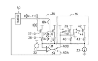
図1は、本発明の一実施形態における増幅回路の構成例を示す図である。本実施形態における増幅回路は、増幅部10、補正回路部30、及び制御部50を有する。増幅部10は、入力信号を受ける入力回路部と、負荷として用いられ所望の抵抗値に制御される可変抵抗回路で構成される負荷回路部とを有し、差動の入力信号を特定のゲイン(倍率)で増幅し出力する。
Claims (10)
- 第1の電源線と第2の電源線との間に設けられ、入力信号を受ける入力回路部と、
前記第1の電源線と前記第2の電源線との間に前記入力回路部と直列に設けられた負荷回路部と、
前記第1の電源線と前記第2の電源線との間に前記負荷回路部と並列に設けられ、前記負荷回路部の抵抗値を補正する補正回路部と、
を備える増幅回路であって、
前記負荷回路部は、
制御回路によって生成されるデジタルコードにより抵抗値が制御される第1の可変抵抗部、及び、前記第1の可変抵抗部と並列に設けられ、前記補正回路部によって生成されたアナログ制御電圧により抵抗値が制御される第2の可変抵抗部を有し、
前記補正回路部は、
前記第1の可変抵抗部に対応する回路構成を有し、前記デジタルコードにより抵抗値が制御される第3の可変抵抗部、及び、前記第3の可変抵抗部と並列に設けられ、前記第2の可変抵抗部に対応する回路構成を有し、前記アナログ制御電圧により抵抗値が制御される第4の可変抵抗部を有する
ことを特徴とする増幅回路。 - 前記補正回路部は、前記第3の可変抵抗部及び前記第4の可変抵抗部により生成される電圧とリファレンス電圧とが入力されるオペアンプを有し、
前記制御回路は、前記オペアンプの出力に基づいて、前記デジタルコードを生成することを特徴とする請求項1記載の増幅回路。 - 第1の状態では、前記オペアンプの出力に基づいて前記制御回路が前記デジタルコードを生成し、
第2の状態では、前記オペアンプの出力を前記アナログ制御電圧として出力することを特徴とする請求項2記載の増幅回路。 - 前記補正回路部の前記第3の可変抵抗部を用いて第1の抵抗値に対応する前記デジタルコードを決定し、
決定された前記第1の抵抗値に対応する前記デジタルコードを前記第3の可変抵抗部に供給して、前記第3の可変抵抗部及び前記第4の可変抵抗部を用いて、前記第3の可変抵抗部及び前記第4の可変抵抗部による合成抵抗値が前記第1の抵抗値になる前記アナログ制御電圧を生成することを特徴とする請求項1〜3の何れか1項に記載の増幅回路。 - 前記第1の抵抗値に対応する前記デジタルコードは、前記デジタルコードを逐次変化させて前記第3の可変抵抗部及び前記第4の可変抵抗部により生成される電圧とリファレンス電圧とを比較することにより、比較結果に基づいて1ビットずつ決定され、
前記第3の可変抵抗部及び前記第4の可変抵抗部による合成抵抗値が前記第1の抵抗値になる前記アナログ制御電圧は、前記第3の可変抵抗部及び前記第4の可変抵抗部により生成される電圧とリファレンス電圧との比較結果を前記第4の可変抵抗部に負帰還させることにより生成されることを特徴とする請求項4記載の増幅回路。 - 前記第1の可変抵抗部及び前記第3の可変抵抗部はそれぞれ、並列に設けられた複数の抵抗と、前記抵抗に電流を流すか否かを前記デジタルコードに応じて制御するトランジスタを有し、
前記第2の可変抵抗部及び前記第4の可変抵抗部はそれぞれ、並列に設けられゲートに前記アナログ制御電圧が供給される複数のトランジスタを有することを特徴とする請求項1〜5の何れか1項に記載の増幅回路。 - 前記第1の可変抵抗部及び前記第3の可変抵抗部はそれぞれ、並列に設けられた複数の抵抗と、前記抵抗に電流を流すか否かを前記デジタルコードに応じて制御するトランジスタを有し、
前記第2の可変抵抗部及び前記第4の可変抵抗部はそれぞれ、並列に設けられゲートに前記アナログ制御電圧が供給される複数のトランジスタを有し、
前記第1の抵抗値に対応する前記デジタルコードを決定するとき、前記第4の可変抵抗部が有する前記複数のトランジスタのゲートにそれぞれ、一定の電圧を供給することを特徴とする請求項4記載の増幅回路。 - 前記第4の可変抵抗部が有する前記複数のトランジスタの内の少なくとも1つのトランジスタのゲートには電源電位を供給し、他の少なくとも1つのトランジスタのゲートには基準電位を供給することを特徴とする請求項7記載の増幅回路。
- 入力シリアル信号を増幅する増幅回路と、
前記増幅回路により増幅された前記入力シリアル信号をサンプリングするコンパレータと、
前記コンパレータの出力に対してシリアル−パラレル変換を行いパラレル信号を出力するデマルチプレクサ回路とを備え、
前記増幅回路は、
第1の電源線と第2の電源線との間に設けられ、前記入力シリアル信号を受ける入力回路部と、
前記第1の電源線と前記第2の電源線との間に前記入力回路部と直列に設けられた負荷回路部と、
前記第1の電源線と前記第2の電源線との間に前記負荷回路部と並列に設けられ、前記負荷回路部の抵抗値を補正する補正回路部と、
を備え、
前記負荷回路部は、
制御回路によって生成されるデジタルコードにより抵抗値が制御される第1の可変抵抗部、及び、前記第1の可変抵抗部と並列に設けられ、前記補正回路部によって生成されたアナログ制御電圧により抵抗値が制御される第2の可変抵抗部を有し、
前記補正回路部は、
前記第1の可変抵抗部に対応する回路構成を有し、前記デジタルコードにより抵抗値が制御される第3の可変抵抗部、及び、前記第3の可変抵抗部と並列に設けられ、前記第2の可変抵抗部に対応する回路構成を有し、前記アナログ制御電圧により抵抗値が制御される第4の可変抵抗部を有する
ことを特徴とする受信回路。 - 入力シリアル信号を増幅する増幅回路と、
前記増幅回路により増幅された前記入力シリアル信号をサンプリングするコンパレータと、
前記コンパレータの出力に対してシリアル−パラレル変換を行いパラレル信号を出力するデマルチプレクサ回路と、
前記デマルチプレクサ回路からの前記パラレル信号を受けて処理動作を行う内部回路とを備え、
前記増幅回路は、
第1の電源線と第2の電源線との間に設けられ、前記入力シリアル信号を受ける入力回路部と、
前記第1の電源線と前記第2の電源線との間に前記入力回路部と直列に設けられた負荷回路部と、
前記第1の電源線と前記第2の電源線との間に前記負荷回路部と並列に設けられ、前記負荷回路部の抵抗値を補正する補正回路部と、
を備え、
前記負荷回路部は、
制御回路によって生成されるデジタルコードにより抵抗値が制御される第1の可変抵抗部、及び、前記第1の可変抵抗部と並列に設けられ、前記補正回路部によって生成されたアナログ制御電圧により抵抗値が制御される第2の可変抵抗部を有し、
前記補正回路部は、
前記第1の可変抵抗部に対応する回路構成を有し、前記デジタルコードにより抵抗値が制御される第3の可変抵抗部、及び、前記第3の可変抵抗部と並列に設けられ、前記第2の可変抵抗部に対応する回路構成を有し、前記アナログ制御電圧により抵抗値が制御される第4の可変抵抗部を有する
ことを特徴とする半導体集積回路。
Applications Claiming Priority (1)
| Application Number | Priority Date | Filing Date | Title |
|---|---|---|---|
| PCT/JP2016/057748 WO2017154194A1 (ja) | 2016-03-11 | 2016-03-11 | 増幅回路、受信回路、及び半導体集積回路 |
Publications (2)
| Publication Number | Publication Date |
|---|---|
| JPWO2017154194A1 JPWO2017154194A1 (ja) | 2019-01-17 |
| JP6725854B2 true JP6725854B2 (ja) | 2020-07-22 |
Family
ID=59790175
Family Applications (1)
| Application Number | Title | Priority Date | Filing Date |
|---|---|---|---|
| JP2018503960A Active JP6725854B2 (ja) | 2016-03-11 | 2016-03-11 | 増幅回路、受信回路、及び半導体集積回路 |
Country Status (5)
| Country | Link |
|---|---|
| US (1) | US10742175B2 (ja) |
| EP (1) | EP3429079B1 (ja) |
| JP (1) | JP6725854B2 (ja) |
| CN (1) | CN108781061B (ja) |
| WO (1) | WO2017154194A1 (ja) |
Families Citing this family (3)
| Publication number | Priority date | Publication date | Assignee | Title |
|---|---|---|---|---|
| CN112019171A (zh) * | 2019-05-31 | 2020-12-01 | 华邦电子股份有限公司 | 差动放大器 |
| KR20220057159A (ko) * | 2020-10-29 | 2022-05-09 | 에스케이하이닉스 주식회사 | 차동 입력 회로를 포함하는 반도체 장치 및 그의 캘리브레이션 방법 |
| US11881969B2 (en) * | 2022-04-22 | 2024-01-23 | Samsung Display Co., Ltd. | Real-time DC-balance aware AFE offset cancellation |
Family Cites Families (21)
| Publication number | Priority date | Publication date | Assignee | Title |
|---|---|---|---|---|
| JPH04135304A (ja) * | 1990-09-27 | 1992-05-08 | Nec Corp | 半導体集積回路 |
| JP4135304B2 (ja) * | 2000-09-25 | 2008-08-20 | コニカミノルタオプト株式会社 | 光学素子成形用金型の製造方法 |
| US6278325B1 (en) * | 2000-12-13 | 2001-08-21 | Industrial Technology Research Institute | Programmable gain amplifier with a large extent for the variation of gains |
| US6583660B2 (en) * | 2001-05-25 | 2003-06-24 | Infineon Technologies Ag | Active auto zero circuit for time continuous open loop amplifiers |
| US6621343B2 (en) | 2001-08-07 | 2003-09-16 | Infineon Technologies Ag | Open loop variable gain amplifier using replica gain cell |
| JP2003084728A (ja) | 2001-09-17 | 2003-03-19 | Citizen Watch Co Ltd | 液晶表示装置の電極駆動電圧発生回路 |
| US6958651B2 (en) * | 2002-12-03 | 2005-10-25 | Semiconductor Energy Laboratory Co., Ltd. | Analog circuit and display device using the same |
| US7034606B2 (en) * | 2004-05-07 | 2006-04-25 | Broadcom Corporation | VGA-CTF combination cell for 10 Gb/s serial data receivers |
| US20070103235A1 (en) * | 2005-11-04 | 2007-05-10 | Motorola, Inc. | Inductorless broadband RF low noise amplifier |
| US7403071B2 (en) * | 2006-03-14 | 2008-07-22 | Freescale Semiconductor, Inc. | High linearity and low noise amplifier with continuously variable gain control |
| JP2007248288A (ja) | 2006-03-16 | 2007-09-27 | Fujitsu Ltd | 温度特性補正方法及びセンサ用増幅回路 |
| JP2007303986A (ja) * | 2006-05-12 | 2007-11-22 | Advantest Corp | 直流試験装置 |
| US7417500B2 (en) * | 2006-06-19 | 2008-08-26 | Tzero Technologies, Inc. | Control of an adjustable gain amplifier |
| KR100952666B1 (ko) * | 2008-02-01 | 2010-04-13 | (주)에프씨아이 | 커패시터 피드백을 이용한 재구성 가능 저잡음 증폭기 |
| JP2009225205A (ja) * | 2008-03-18 | 2009-10-01 | Yokogawa Electric Corp | Cml回路 |
| JP2011055055A (ja) * | 2009-08-31 | 2011-03-17 | Texas Instr Japan Ltd | 増幅回路及び信号強度検出回路並びにオフセット電圧調整方法 |
| US8384465B2 (en) * | 2010-06-15 | 2013-02-26 | Aeroflex Colorado Springs Inc. | Amplitude-stabilized even order pre-distortion circuit |
| CN102195583B (zh) * | 2011-05-24 | 2016-01-20 | 中兴通讯股份有限公司 | 一种铌酸锂调制器跨阻放大器增益控制装置及方法 |
| CN102969990A (zh) * | 2011-09-01 | 2013-03-13 | 联咏科技股份有限公司 | 具动态转导补偿的多输入差动放大器 |
| US8878608B2 (en) * | 2011-11-03 | 2014-11-04 | Mediatek Inc. | Comparator and amplifier |
| US9325287B2 (en) * | 2014-01-24 | 2016-04-26 | Applied Micro Circuits Corporation | Programmable gain amplifier with controlled gain steps |
-
2016
- 2016-03-11 CN CN201680083314.XA patent/CN108781061B/zh active Active
- 2016-03-11 JP JP2018503960A patent/JP6725854B2/ja active Active
- 2016-03-11 EP EP16893521.1A patent/EP3429079B1/en active Active
- 2016-03-11 WO PCT/JP2016/057748 patent/WO2017154194A1/ja active Application Filing
-
2018
- 2018-08-23 US US16/110,801 patent/US10742175B2/en active Active
Also Published As
| Publication number | Publication date |
|---|---|
| EP3429079A1 (en) | 2019-01-16 |
| US20180367103A1 (en) | 2018-12-20 |
| EP3429079B1 (en) | 2021-05-05 |
| EP3429079A4 (en) | 2019-03-27 |
| US10742175B2 (en) | 2020-08-11 |
| CN108781061A (zh) | 2018-11-09 |
| JPWO2017154194A1 (ja) | 2019-01-17 |
| WO2017154194A1 (ja) | 2017-09-14 |
| CN108781061B (zh) | 2022-04-08 |
Similar Documents
| Publication | Publication Date | Title |
|---|---|---|
| JP6871934B2 (ja) | 線形ゲイン符号をインターリーブされたオートゲインコントロール回路 | |
| US9674008B2 (en) | Body-biased slicer design for predictive decision feedback equalizers | |
| US7915913B2 (en) | Termination resistance adjusting circuit | |
| US9564863B1 (en) | Circuits and methods for variable gain amplifiers | |
| US20140036982A1 (en) | High Bandwidth Equalizer and Limiting Amplifier | |
| US9954503B2 (en) | Differential amplification circuit and semiconductor integrated circuit | |
| JP2019527983A (ja) | 電圧モードドライバのインピーダンスおよびスイング制御 | |
| JP6725854B2 (ja) | 増幅回路、受信回路、及び半導体集積回路 | |
| US7697601B2 (en) | Equalizers and offset control | |
| TWI448868B (zh) | Voltage regulator | |
| JP2006066833A (ja) | 抵抗値補償方法、抵抗値補償機能を有する回路、回路の抵抗値試験方法,抵抗値補償プログラム及び回路の抵抗値試験プログラム | |
| US20110133837A1 (en) | Variable gain amplifier | |
| US20090002076A1 (en) | Signal waveform equalizer circuit and receiver circuit | |
| JP6072387B1 (ja) | 可変利得増幅器 | |
| US9553566B2 (en) | Hybrid driver circuit | |
| WO2022118440A1 (ja) | 位相補間回路、受信回路及び半導体集積回路 | |
| JP5035341B2 (ja) | 増幅回路 | |
| US20200201375A1 (en) | Bandgap circuits with voltage calibration | |
| JP7453562B2 (ja) | 差動増幅回路、受信回路及び半導体集積回路 | |
| JP5369472B2 (ja) | 半導体装置 | |
| JP2018522490A (ja) | 制御された利得ステップを有するプログラム可能な利得増幅器 |
Legal Events
| Date | Code | Title | Description |
|---|---|---|---|
| A521 | Request for written amendment filed |
Free format text: JAPANESE INTERMEDIATE CODE: A523 Effective date: 20180817 |
|
| A621 | Written request for application examination |
Free format text: JAPANESE INTERMEDIATE CODE: A621 Effective date: 20190220 |
|
| A131 | Notification of reasons for refusal |
Free format text: JAPANESE INTERMEDIATE CODE: A131 Effective date: 20191217 |
|
| A521 | Request for written amendment filed |
Free format text: JAPANESE INTERMEDIATE CODE: A523 Effective date: 20200204 |
|
| TRDD | Decision of grant or rejection written | ||
| A01 | Written decision to grant a patent or to grant a registration (utility model) |
Free format text: JAPANESE INTERMEDIATE CODE: A01 Effective date: 20200526 |
|
| A61 | First payment of annual fees (during grant procedure) |
Free format text: JAPANESE INTERMEDIATE CODE: A61 Effective date: 20200608 |
|
| R150 | Certificate of patent or registration of utility model |
Ref document number: 6725854 Country of ref document: JP Free format text: JAPANESE INTERMEDIATE CODE: R150 |