JP6689839B2 - Magnetic field sensor for detecting movement of target object - Google Patents
Magnetic field sensor for detecting movement of target object Download PDFInfo
- Publication number
- JP6689839B2 JP6689839B2 JP2017522906A JP2017522906A JP6689839B2 JP 6689839 B2 JP6689839 B2 JP 6689839B2 JP 2017522906 A JP2017522906 A JP 2017522906A JP 2017522906 A JP2017522906 A JP 2017522906A JP 6689839 B2 JP6689839 B2 JP 6689839B2
- Authority
- JP
- Japan
- Prior art keywords
- magnetic field
- signal
- magnetoresistive element
- field sensor
- target object
- Prior art date
- Legal status (The legal status is an assumption and is not a legal conclusion. Google has not performed a legal analysis and makes no representation as to the accuracy of the status listed.)
- Active
Links
Images


Classifications
-
- G—PHYSICS
- G01—MEASURING; TESTING
- G01D—MEASURING NOT SPECIALLY ADAPTED FOR A SPECIFIC VARIABLE; ARRANGEMENTS FOR MEASURING TWO OR MORE VARIABLES NOT COVERED IN A SINGLE OTHER SUBCLASS; TARIFF METERING APPARATUS; MEASURING OR TESTING NOT OTHERWISE PROVIDED FOR
- G01D5/00—Mechanical means for transferring the output of a sensing member; Means for converting the output of a sensing member to another variable where the form or nature of the sensing member does not constrain the means for converting; Transducers not specially adapted for a specific variable
- G01D5/12—Mechanical means for transferring the output of a sensing member; Means for converting the output of a sensing member to another variable where the form or nature of the sensing member does not constrain the means for converting; Transducers not specially adapted for a specific variable using electric or magnetic means
- G01D5/14—Mechanical means for transferring the output of a sensing member; Means for converting the output of a sensing member to another variable where the form or nature of the sensing member does not constrain the means for converting; Transducers not specially adapted for a specific variable using electric or magnetic means influencing the magnitude of a current or voltage
- G01D5/142—Mechanical means for transferring the output of a sensing member; Means for converting the output of a sensing member to another variable where the form or nature of the sensing member does not constrain the means for converting; Transducers not specially adapted for a specific variable using electric or magnetic means influencing the magnitude of a current or voltage using Hall-effect devices
- G01D5/147—Mechanical means for transferring the output of a sensing member; Means for converting the output of a sensing member to another variable where the form or nature of the sensing member does not constrain the means for converting; Transducers not specially adapted for a specific variable using electric or magnetic means influencing the magnitude of a current or voltage using Hall-effect devices influenced by the movement of a third element, the position of Hall device and the source of magnetic field being fixed in respect to each other
-
- G—PHYSICS
- G01—MEASURING; TESTING
- G01D—MEASURING NOT SPECIALLY ADAPTED FOR A SPECIFIC VARIABLE; ARRANGEMENTS FOR MEASURING TWO OR MORE VARIABLES NOT COVERED IN A SINGLE OTHER SUBCLASS; TARIFF METERING APPARATUS; MEASURING OR TESTING NOT OTHERWISE PROVIDED FOR
- G01D5/00—Mechanical means for transferring the output of a sensing member; Means for converting the output of a sensing member to another variable where the form or nature of the sensing member does not constrain the means for converting; Transducers not specially adapted for a specific variable
- G01D5/12—Mechanical means for transferring the output of a sensing member; Means for converting the output of a sensing member to another variable where the form or nature of the sensing member does not constrain the means for converting; Transducers not specially adapted for a specific variable using electric or magnetic means
- G01D5/14—Mechanical means for transferring the output of a sensing member; Means for converting the output of a sensing member to another variable where the form or nature of the sensing member does not constrain the means for converting; Transducers not specially adapted for a specific variable using electric or magnetic means influencing the magnitude of a current or voltage
- G01D5/16—Mechanical means for transferring the output of a sensing member; Means for converting the output of a sensing member to another variable where the form or nature of the sensing member does not constrain the means for converting; Transducers not specially adapted for a specific variable using electric or magnetic means influencing the magnitude of a current or voltage by varying resistance
Description
本発明は、概して磁場センサに関し、より詳細には、基板及び基板上に配置され、様々な相対的位置に全てが配置される強磁性物体の動きを検知する磁場検知素子を有する磁場センサに関する。 The present invention relates generally to magnetic field sensors, and more particularly to a magnetic field sensor having a substrate and a magnetic field sensing element disposed on the substrate for sensing movement of ferromagnetic objects all located in various relative positions.
ホール効果素子及び磁気抵抗素子など、様々な種類の磁場検知素子が知られている。一般に、磁場センサは、磁場検知素子及び他の電子部品を含む。また、ある種の磁場センサは、以下でより詳細に説明される「バックバイアス」配置と呼ばれる永久磁石(ハード強磁性物体)をも含む。他の磁場センサは、磁石の動きを検知する。 Various types of magnetic field sensing elements such as Hall effect elements and magnetoresistive elements are known. Generally, magnetic field sensors include magnetic field sensing elements and other electronic components. Some magnetic field sensors also include permanent magnets (hard ferromagnetic objects) called "back bias" arrangements, which are described in more detail below. Other magnetic field sensors detect movement of the magnet.
磁場センサは、検知した磁場を表す電気信号を提供する。磁石(バックバイアス配置)を有するいくつかの実施形態において、検知された磁場は磁石によって生成された磁場であり、この場合、動いている強磁性物体が存在すると、磁石によって生成され磁場センサによって検知された磁場は、動作中の強磁性物体の形状又は輪郭に応じて変化する。これに対して、動作中の磁石を直接検知する磁場センサは、磁石の動きから生じる磁場の大きさ及び方向の変化を検知する。 The magnetic field sensor provides an electrical signal representative of the sensed magnetic field. In some embodiments with a magnet (back bias arrangement), the sensed magnetic field is the magnetic field produced by the magnet, in the presence of a moving ferromagnetic object, produced by the magnet and sensed by the magnetic field sensor. The generated magnetic field changes depending on the shape or contour of the ferromagnetic object in operation. On the other hand, the magnetic field sensor that directly detects the magnet during operation detects a change in the magnitude and direction of the magnetic field caused by the movement of the magnet.
磁場センサ(バックバイアス)は、ギア歯及び/又はギアスロット又は谷などの強磁性ギアの特徴物の動きを検出するために用いられることが多い。この用途における磁場センサは、一般に、「ギア歯」センサと称される。 Magnetic field sensors (back bias) are often used to detect the movement of ferromagnetic gear features such as gear teeth and / or gear slots or valleys. The magnetic field sensor in this application is commonly referred to as a "gear tooth" sensor.
ある種の構成において、ギアは、例えば、エンジン内のカムシャフトなどの強磁性対象物体(ferromagnetic target object)上に配置される。このようにして、ギアの動作する特徴物を検出することにより、強磁性対象物体(例えば、カムシャフト)の回転が検知される。ギア歯センサは、例えば、点火時期制御、燃料管理、アンチロックブレーキシステム、車輪速度センサ、及び他の動作のためのエンジン制御プロセッサに情報を提供するために、自動車分野において利用される。 In certain configurations, the gears are located on a ferromagnetic target object, such as a camshaft in an engine, for example. In this way, the rotation of the ferromagnetic target object (for example, the camshaft) is detected by detecting the feature in which the gear operates. Gear tooth sensors are utilized in the automotive field, for example, to provide information to the engine control processor for ignition timing control, fuel management, antilock braking systems, wheel speed sensors, and other operations.
ギア歯センサによりエンジン制御プロセッサへと提供される情報は、強磁性対象物体(例えば、カムシャフト)が回転する際の絶対回転角、回転速度、及び回転方向を含み得るが、これに限定されるものではない。この情報により、エンジン制御プロセッサは、点火システムの点火時期、及び燃料噴射システムの燃料噴射時期を調整可能である。 The information provided by the gear tooth sensor to the engine control processor may include, but is not limited to, the absolute angle of rotation, the speed of rotation, and the direction of rotation as the ferromagnetic target object (eg, camshaft) rotates. Not a thing. With this information, the engine control processor can adjust the ignition timing of the ignition system and the fuel injection timing of the fuel injection system.
多くのタイプの磁場センサは、パワーアップの直後に、ゼロ回転速度からの強磁性対象物体の移動の直後に、及び/又は、ゼロ回転速度へと遅くなる移動の直後に、正確な出力信号(例えば、回転の絶対角度、速度、又は方向のインジケーション)を提供しないが、その代わりに、強磁性対象物体がかなりの回転で移動したときだけ、又は、かなりの速度で移動しているときだけ、正確な出力信号を提供する。例えば、2003年2月25日発行の「Detection of Passing Magnetic Articles while Adapting the Detection Threshold(検出閾値を適合させつつ通過する磁性物品を検出すること)」という名称の米国特許第6,525,531号に説明される1つのタイプの磁場センサでは、プラスのデジタルアナログコンバータ(PDAC)及びマイナスのデジタルアナログコンバータ(NDAC)が、それぞれ、閾値信号を発生させる際の使用のために、磁場信号のプラスピーク及びマイナスピークをトラッキングする。変動する磁場信号が、閾値信号と比較される。しかし、PDAC及びNDACの出力は、信号のいくつかのサイクル(すなわち、信号ピーク)が起こるまでは(すなわち、いくつかのギア歯が通過するまでは)、磁場信号のプラスピーク及びマイナスピークの正確なインジケーションであることはできない。このタイプの磁場センサは、一般的に、十分に正確になるための時間を必要とし、本明細書で、いわゆる「精密回転検出器」と称される。 Many types of magnetic field sensors provide an accurate output signal (immediately after power-up, immediately after moving a ferromagnetic target object from zero rotation speed, and / or immediately after moving slowing to zero rotation speed). (E.g., absolute angle of rotation, velocity, or direction indication), but instead only when the ferromagnetic object is moving with significant rotation, or moving with significant velocity. Provide accurate output signal. For example, U.S. Pat. No. 6,525,531 entitled "Detection of Passing Magnetic Articles while Adapting the Detection Threshold" (Feeding February 25, 2003). In one type of magnetic field sensor described in, a positive digital-to-analog converter (PDAC) and a negative digital-to-analog converter (NDAC) each have a positive peak in the magnetic field signal for use in generating a threshold signal. And track negative peaks. The varying magnetic field signal is compared to the threshold signal. However, the outputs of the PDAC and NDAC are accurate for the positive and negative peaks of the magnetic field signal until some cycles of the signal occur (ie signal peaks) (ie until some gear teeth pass). It cannot be a good indication. This type of magnetic field sensor generally requires time to be sufficiently accurate and is referred to herein as a so-called "precision rotation detector".
それとは対照的に、「トゥルーパワーオンステート」(TPOS)検出器は、ゼロ回転速度、もしくは、いくつかの用途では例えば、100rpm未満の低い回転速度からの強磁性対象物体(例えば、カムシャフト)の移動の直後に、又は、ゼロ回転速度へと遅くなる移動の少し前にも、正確な出力信号を提供することが可能である。そのうえ、強磁性対象物体が移動していないときでも、TPOS検出器は、TPOS検出器がギアの歯又は谷の前にいるかどうかというインジケーションを提供することが可能である。しかし、強磁性対象物体が静止しているときには、従来のTPOS検出器は、強磁性対象物体の回転の絶対的な角度又は相対的な角度を識別することができない。TPOS検出器は、共通の集積回路の中の精密回転検出器と関連して使用され得、それぞれが、異なる時間に、エンジン制御プロセッサに情報を提供する。簡単にするために、TPOS検出器及び精密回転検出器は、本明細書では、共通の集積回路の中に示される。しかし、TPOS検出器又は精密回転検出器は、別々の回路の中で単独で使用することも可能である。 In contrast, a "true power on state" (TPOS) detector is a ferromagnetic target object (e.g., camshaft) from zero rotation speed, or in some applications, low rotation speed, for example, less than 100 rpm. It is possible to provide an accurate output signal shortly after the movement of or even shortly before the movement slowing to zero rotational speed. Moreover, even when the ferromagnetic object is not moving, the TPOS detector can provide an indication of whether the TPOS detector is in front of the gear teeth or valleys. However, when the ferromagnetic target object is stationary, conventional TPOS detectors are unable to identify the absolute or relative angle of rotation of the ferromagnetic target object. The TPOS detectors can be used in conjunction with precision rotation detectors in a common integrated circuit, each providing information to the engine control processor at different times. For simplicity, the TPOS detector and the precision rotation detector are shown herein in a common integrated circuit. However, the TPOS detector or precision rotation detector can also be used alone in separate circuits.
上記に述べたように、従来のTPOS検出器は、精密回転検出器が正確な出力信号を提供することができる前に、強磁性対象物体の小さな最初の回転だけに関して正確な出力信号を提供する。TPOS検出器は、強磁性対象物体の回転の始め及び終わりの期間の間(例えばエンジン及びカムシャフトの開始及び停止の期間の間)、精密回転検出器によって提供される情報より正確であり得る情報をエンジン制御プロセッサに提供することができるが、しかしその情報は、物体がスピードを出して回転しているとき、それほど正確でないことがある。TPOS検出器及び精密回転検出器の両方を共通の集積回路内に有する磁場センサ配置にとって、物体が回転していないか遅く回転しているときには、エンジン制御プロセッサはTPOS検出器を使用することができる。物体がスピードを出して回転しているとき、エンジン制御プロセッサは、精密回転検出器によって提供される回転情報を主として使用することができる。ほとんどの従来の用途では、一度磁場センサが精密回転検出器の使用に切り替わると、磁場センサは、強磁性対象物体が回転を停止するまで、又は回転をほぼ停止するまで、TPOS検出器の使用に戻らない。 As mentioned above, the conventional TPOS detector provides an accurate output signal for only a small initial rotation of the ferromagnetic object before the precision rotation detector can provide an accurate output signal. . The TPOS detector may be more accurate than the information provided by the precision rotation detector during the beginning and end of the rotation of the ferromagnetic object (eg, during the start and stop of the engine and camshaft). Can be provided to the engine control processor, but the information may not be so accurate when the object is spinning at speed. For magnetic field sensor arrangements that have both a TPOS detector and a precision rotation detector in a common integrated circuit, the engine control processor can use the TPOS detector when the object is not spinning or is spinning slowly. . When the object is spinning at speed, the engine control processor can primarily use the rotation information provided by the precision rotation detector. In most conventional applications, once the magnetic field sensor switches to using a precision rotation detector, the magnetic field sensor will be used for the TPOS detector until the ferromagnetic target object stops rotating, or nearly stops rotating. Dont return.
従来のTPOS検出器は、2008年4月22日発行の「Method and Apparatus for Magnetic Article Detection(磁性物品検出のための方法及び装置)」という名称の米国特許第7,362,094号に記載される。従来のTPOS検出器は、磁場信号を固定された、しばしば調整された閾値信号と比較するための比較器を含む。従来のTPOS検出器は、TPOSカム(歯車と同様の)とともに使用して、それについての回転情報を検出することができ、その検出器は、強磁性対象物体、例えば回転するように構成されたエンジンのカムシャフト上に配置される。 A conventional TPOS detector is described in US Pat. No. 7,362,094, entitled “Method and Apparatus for Magnetic Article Detection” issued Apr. 22, 2008. It Conventional TPOS detectors include a comparator for comparing the magnetic field signal with a fixed, often adjusted threshold signal. A conventional TPOS detector can be used with a TPOS cam (similar to a gear) to detect rotation information about it, which detector is configured to rotate a ferromagnetic target object, eg, rotate. It is located on the camshaft of the engine.
従来のTPOS検出器からの出力信号の例は、少なくとも2つの状態、通常ハイ状態及びロー状態を有する。従来のTPOS出力信号の状態は、強磁性対象物体が回転するにつれて、強磁性対象物体に取り付けられたTPOSカム(又はギア)上の特徴物に従って、ある時点でハイであり、他の時点ではローである。 An example output signal from a conventional TPOS detector has at least two states, typically a high state and a low state. The state of a conventional TPOS output signal is high at some times and low at other times as the ferromagnetic target object rotates, depending on features on the TPOS cam (or gear) attached to the ferromagnetic target object. Is.
同様に、従来の精密回転検出器からの出力信号は、少なくとも2つの状態、通常ハイ状態及びロー状態を有する。従来の精密回転検出器出力信号の状態は、強磁性対象物体が回転するにつれて、強磁性対象物体に取り付けられたTPOSカム(又はギア)上の特徴物に従って、ある時点でハイであり、他の時点ではローである。 Similarly, the output signal from a conventional precision rotation detector has at least two states, typically a high state and a low state. The state of the conventional precision rotation detector output signal is high at some point, depending on the features on the TPOS cam (or gear) attached to the ferromagnetic target object as the ferromagnetic target object rotates, and other states. It is low at this point.
上述の通り、従来のTPOS検出器は、ギア歯をギア谷と区別することが可能であり、ギアが回転しているとき及びギアが回転していないときにそのような検出を行うことができる。これに対して、ある種の従来の精密回転検出器は、ギアが回転しているときにはギア歯をギア谷と区別することが可能であるが、ギアが静止しているときにはできない。ギア歯をギア谷と区別することが可能な検出器は、「歯検出器」と呼ばれることがある。したがって、TPOS検出器は通常、歯検出器である。ある種の精密回転検出器もまた歯検出器であり得る。 As mentioned above, conventional TPOS detectors can distinguish gear teeth from gear troughs and can make such detections when the gear is rotating and when the gear is not rotating. . In contrast, some conventional precision rotation detectors can distinguish gear teeth from gear troughs when the gear is rotating, but not when the gear is stationary. A detector capable of distinguishing a gear tooth from a gear trough is sometimes referred to as a "tooth detector". Therefore, the TPOS detector is typically a tooth detector. Certain precision rotation detectors can also be tooth detectors.
他のいくつかの従来の精密回転検出器は、ギア歯をギア谷と区別することができないが、その代わり、ギア歯のエッジを歯又は谷と区別することができる。このような検出器は、「エッジ検出器」と呼ばれることがある。通常、TPOS検出器はエッジ検出器ではない。しかしながら、ある種の精密回転検出器はエッジ検出器であり得る。 Some other conventional precision rotation detectors cannot distinguish gear teeth from gear troughs, but instead can distinguish the edges of gear teeth from teeth or troughs. Such detectors are sometimes called "edge detectors". Usually, the TPOS detector is not an edge detector. However, some precision rotation detectors can be edge detectors.
従来の磁場センサは、たとえ磁場センサとギアとの間に組み立て状態又はその時々によって変化し得る空隙が存在したとしてもギア歯とギア谷を正確に区別する正確な出力信号を実現しなければならなかった。さらに、従来の磁場センサは、磁場センサ内の磁石及び磁場検知素子の位置に関するユニット間のばらつきが存在したとしてもこのような区別を実現しなければならなかった。さらに、従来の磁場センサは、磁石によって生成される磁場のユニット間のばらつきが存在したとしてもこのような区別を実現しなければならなかった。さらに、従来の磁場センサは、ギアに対する磁場センサの軸回転のばらつきが存在したとしてもこのような区別を実現しなければならなかった。さらに、従来の磁場センサは、磁場センサの雰囲気温度のばらつきが存在したとしてもこのような区別を実現しなければならなかった。 Conventional magnetic field sensors must provide an accurate output signal that accurately distinguishes gear teeth and valleys even if there is an air gap between the magnetic field sensor and the gear that may change due to assembly conditions or from time to time. There wasn't. Further, the conventional magnetic field sensor has to realize such a distinction even if there is a unit-to-unit variation in the positions of the magnet and the magnetic field detection element in the magnetic field sensor. Furthermore, conventional magnetic field sensors have had to achieve such a distinction, even if there is unit-to-unit variation in the magnetic field generated by the magnet. Furthermore, the conventional magnetic field sensor has to realize such a distinction even if there is a variation in the axial rotation of the magnetic field sensor with respect to the gear. Further, the conventional magnetic field sensor has to realize such a distinction even if there is a variation in ambient temperature of the magnetic field sensor.
上記の影響によって高価な設計選択を迫られる。特に、上記のいくつかの影響によって図1において以下説明される高価な磁石を使用することになる。 The above effects force expensive design choices. In particular, some of the effects described above result in the use of expensive magnets, described below in FIG.
簡素でかつ低価格の磁石を使用してギア歯をギア谷と正確に区別する正確な出力信号を実現することができる磁場センサを提供することが望ましい。 It would be desirable to provide a magnetic field sensor that is capable of achieving accurate output signals that accurately distinguish gear teeth from gear troughs using simple and inexpensive magnets.
磁場センサは、簡素でかつ低価格の磁石を使用してギア歯をギア谷と正確に区別する正確な出力信号を実現する。このような区別は、磁場センサに関する機械的及び熱的パラメータのばらつきが存在したとしても実現される。 The magnetic field sensor uses a simple and low cost magnet to provide an accurate output signal that accurately distinguishes the gear teeth from the gear troughs. Such a distinction is achieved even in the presence of variations in mechanical and thermal parameters for the magnetic field sensor.
本発明の態様を理解するために役立つ例において、対象特徴物幅(target feature width)をもつ強磁性対象物体特徴物(ferromagnetic target object features)を有する強磁性対象物体の動きを検知するための磁場センサは、基板と、強磁性対象物体特徴物の動きに応答する第1の信号を生成するための、基板上に配置された第1の磁気抵抗素子と、強磁性対象物体特徴物の動きに応答する第2の信号を生成するための、基板上に配置された第2の磁気抵抗素子と、を備える。磁場センサは、さらに、第1の信号と第2の信号とを合成して、強磁性対象物体特徴物が前記第1の磁気抵抗素子及び前記第2の磁気抵抗素子の中央にあるときに最大値をとる特徴信号(feature signal)を生成するように構成される、基板上に配置された第1の合成回路(combining circuit)を備える。磁場センサは、さらに、第1の信号と第2の信号とを合成して、第1の磁気抵抗素子が対象特徴物のエッジの一方側にあり第2の磁気抵抗素子が同じエッジの反対側にあるときに最大値をとるエッジ信号を生成するように構成される、基板上に配置された第2の合成回路を備える。 In an example useful for understanding aspects of the present invention, a magnetic field for sensing motion of a ferromagnetic target object having a ferromagnetic target object features with a target feature width. The sensor includes a substrate, a first magnetoresistive element disposed on the substrate for generating a first signal responsive to movement of the ferromagnetic target object feature, and a motion of the ferromagnetic target object feature. A second magnetoresistive element disposed on the substrate for generating a responsive second signal. The magnetic field sensor further combines the first signal and the second signal to maximize the ferromagnetic target object feature when it is in the center of the first magnetoresistive element and the second magnetoresistive element. It comprises a first combining circuit arranged on the substrate, which is arranged to generate a value-oriented feature signal. The magnetic field sensor further combines the first signal and the second signal so that the first magnetoresistive element is on one side of the edge of the target feature and the second magnetoresistive element is on the opposite side of the same edge. A second combiner circuit disposed on the substrate, the second combiner circuit being configured to generate the maximum edge signal when
いくつかの実施形態において、上記の磁場センサは、1又は複数の以下の態様を任意の組み合わせで備え得る。
上記の磁場センサのいくつかの実施形態において、第1の磁気抵抗素子及び第2の磁気抵抗素子は、強磁性対象物体の動きの方向に対する接線に平行なライン上に配置される。
In some embodiments, the magnetic field sensor described above may comprise one or more of the following aspects in any combination.
In some embodiments of the magnetic field sensor described above, the first magnetoresistive element and the second magnetoresistive element are arranged on a line parallel to a tangent to the direction of motion of the ferromagnetic target object.
上記の磁場センサのいくつかの実施形態において、第1の磁気抵抗素子及び第2の磁気抵抗素子は、対象特徴物幅の約1/2から約2倍の間の間隔で配置される。
いくつかの実施形態において、上記の磁場センサは、第1の磁気抵抗素子及び第2の磁気抵抗素子のそれぞれにおいて磁場を生成するための磁石をさらに備えることができ、強磁性対象物体は、強磁性対象物体の動きが第1の磁気抵抗素子及び第2の磁気抵抗素子において磁場の変化をもたらすような位置に配置される。
In some embodiments of the magnetic field sensor described above, the first magnetoresistive element and the second magnetoresistive element are spaced between about 1/2 and about 2 times the target feature width.
In some embodiments, the magnetic field sensor may further include a magnet for generating a magnetic field in each of the first magnetoresistive element and the second magnetoresistive element, wherein the ferromagnetic target object has a strong magnetic field. The movement of the magnetic target object is arranged at a position where the magnetic field changes in the first magnetoresistive element and the second magnetoresistive element.
上記の磁場センサのいくつかの実施形態において、強磁性対象物体は、交互のN極及びS極を有するリング磁石を含み、第1の磁気抵抗素子及び第2の磁気抵抗素子のそれぞれにおいて磁場を生成し、強磁性対象物体は、強磁性対象物体の動きが第1の磁気抵抗素子及び第2の磁気抵抗素子において磁場の変化をもたらすような位置に配置される。 In some embodiments of the magnetic field sensor described above, the ferromagnetic target object comprises a ring magnet having alternating north and south poles, and a magnetic field is applied in each of the first magnetoresistive element and the second magnetoresistive element. The ferromagnetic target object is generated and positioned so that the movement of the ferromagnetic target object causes a change in the magnetic field in the first magnetoresistive element and the second magnetoresistive element.
いくつかの実施形態において、上記の磁場センサは、基板上に配置され、特徴信号及びエッジ信号を受信するために結合され、特徴信号とエッジ信号との間の位相差の符号を計算して強磁性対象物体の動きの方向のインジケーションを生成するようになっている電子回路をさらに備えることができる。 In some embodiments, the magnetic field sensor is disposed on a substrate, is coupled to receive the feature signal and the edge signal, and calculates a sign of a phase difference between the feature signal and the edge signal to obtain a strong signal. An electronic circuit adapted to generate an indication of the direction of movement of the magnetic target object may further be provided.
いくつかの実施形態において、上記の磁場センサは、基板上に配置され、特徴信号及びエッジ信号を受信するために結合された電子回路をさらに備えることができ、電子回路は、エッジ信号を1又は複数の閾値と比較して第1の2値信号を生成するよう動作可能であり、特徴信号を他の1又は複数の閾値と比較して第2の2値信号を生成するよう動作可能であり、磁場センサによって生成された出力信号は、第1の2値信号又は第2の2値信号の選択された一方の状態遷移との整合を特定する信号エンコーディングを含む。 In some embodiments, the magnetic field sensor may further comprise electronic circuitry disposed on the substrate and coupled to receive the feature signal and the edge signal, the electronic circuit including one or more edge signals. Operable to generate a first binary signal by comparing with a plurality of thresholds and operable to generate a second binary signal by comparing the feature signal with another threshold or thresholds The output signal produced by the magnetic field sensor includes signal encoding that identifies a match of the selected one of the first binary signal or the second binary signal with a selected state transition.
上記の磁場センサのいくつかの実施形態において、出力信号は、対象物体の動きの速度を表すパルスレート、及び、第1の2値信号又は第2の2値信号の選択された一方の状態遷移に整合するパルスエッジ、を有するパルスを含む。 In some embodiments of the magnetic field sensor described above, the output signal is a pulse rate representative of the velocity of movement of the target object, and a selected one state transition of the first binary signal or the second binary signal. A pulse edge that matches
上記の磁場センサのいくつかの実施形態において、第1の2値信号と第2の2値信号との間の相対位相は、強磁性対象物体の動きの方向を表し、パルスは、強磁性対象物体の動きの方向を表すパルス幅を含む。 In some embodiments of the magnetic field sensor described above, the relative phase between the first binary signal and the second binary signal represents the direction of motion of the ferromagnetic object and the pulse is the ferromagnetic object. It includes a pulse width that represents the direction of motion of the object.
上記の磁場センサのいくつかの実施形態において、基板は、第1及び第2の平行な最大面を含み、第1の磁気抵抗素子及び第2の磁気抵抗素子は、基板の第1の最大面内又は基板の第1の最大面上に配置され、強磁性対象物体は、第1及び第2の平行な最大面を有し、基板の第1の最大面は、強磁性対象物体の第1の最大面に対して実質的に平行である。 In some embodiments of the magnetic field sensor described above, the substrate comprises first and second parallel maximal planes and the first magnetoresistive element and the second magnetoresistive element are the first maximal plane of the substrate. Disposed in or on the first largest surface of the substrate, the ferromagnetic target object has first and second parallel largest surfaces, and the first largest surface of the substrate is the first largest surface of the ferromagnetic target object. Is substantially parallel to the maximum plane of.
いくつかの実施形態において、上記の磁場センサは、基板上に配置された第1の抵抗素子と、基板上に配置された第2の抵抗素子と、をさらに備えることができ、第1の磁気抵抗素子及び第2の磁気抵抗素子は、第1の抵抗素子及び第2の抵抗素子とともにフルブリッジ回路内に結合され、フルブリッジ回路は、第1の信号が生成される第1のノード及び第2の信号が生成される第2のノードを有する。 In some embodiments, the magnetic field sensor can further include a first resistive element disposed on the substrate and a second resistive element disposed on the substrate, the first magnetic element The resistive element and the second magnetoresistive element are coupled in a full bridge circuit with the first resistive element and the second resistive element, the full bridge circuit including a first node and a first node at which a first signal is generated. It has a second node where two signals are generated.
上記の磁場センサのいくつかの実施形態において、第1の磁気抵抗素子及び第2の磁気抵抗素子は、強磁性対象物体の動きの方向に対する接線に平行なライン上に配置される。
上記の磁場センサのいくつかの実施形態において、第1の磁気抵抗素子及び第2の磁気抵抗素子は、対象特徴物幅の約1/2から約2倍の間の間隔で配置される。
In some embodiments of the magnetic field sensor described above, the first magnetoresistive element and the second magnetoresistive element are arranged on a line parallel to a tangent to the direction of motion of the ferromagnetic target object.
In some embodiments of the magnetic field sensor described above, the first magnetoresistive element and the second magnetoresistive element are spaced between about 1/2 and about 2 times the target feature width.
いくつかの実施形態において、上記の磁場センサは、第1の磁気抵抗素子及び第2の磁気抵抗素子のそれぞれにおいて磁場を生成するための磁石をさらに備えることができ、強磁性対象物体は、強磁性対象物体の動きが第1の磁気抵抗素子及び第2の磁気抵抗素子において磁場の変化をもたらすような位置に配置される。 In some embodiments, the magnetic field sensor may further include a magnet for generating a magnetic field in each of the first magnetoresistive element and the second magnetoresistive element, wherein the ferromagnetic target object has a strong magnetic field. The movement of the magnetic target object is arranged at a position where the magnetic field changes in the first magnetoresistive element and the second magnetoresistive element.
上記の磁場センサのいくつかの実施形態において、強磁性対象物体は、交互のN極及びS極を有するリング磁石を含み、第1の磁気抵抗素子及び第2の磁気抵抗素子のそれぞれにおいて磁場を生成し、強磁性対象物体は、強磁性対象物体の動きが第1の磁気抵抗素子及び第2の磁気抵抗素子において磁場の変化をもたらすような位置に配置される。 In some embodiments of the magnetic field sensor described above, the ferromagnetic target object comprises a ring magnet having alternating north and south poles, and a magnetic field is applied in each of the first magnetoresistive element and the second magnetoresistive element. The ferromagnetic target object is generated and positioned so that the movement of the ferromagnetic target object causes a change in the magnetic field in the first magnetoresistive element and the second magnetoresistive element.
いくつかの実施形態において、上記の磁場センサは、基板上に配置され、特徴信号及びエッジ信号を受信するために結合され、特徴信号とエッジ信号との間の位相差の符号を計算して強磁性対象物体の動きの方向のインジケーションを生成するように構成される電子回路をさらに備えることができる。 In some embodiments, the magnetic field sensor is disposed on a substrate, is coupled to receive the feature signal and the edge signal, and calculates a sign of a phase difference between the feature signal and the edge signal to obtain a strong signal. An electronic circuit configured to generate an indication of a direction of motion of the magnetic target object may further be included.
いくつかの実施形態において、上記の磁場センサは、基板上に配置され、特徴信号及びエッジ信号を受信するために結合された電子回路をさらに備えることができ、電子回路は、エッジ信号を1又は複数の閾値と比較して第1の2値信号を生成するよう動作可能であり、特徴信号を他の1又は複数の閾値と比較して第2の2値信号を生成するよう動作可能であり、磁場センサによって生成された出力信号は、第1の2値信号又は第2の2値信号の選択された一方の状態遷移との整合を特定する信号エンコーディングを含む。 In some embodiments, the magnetic field sensor may further comprise electronic circuitry disposed on the substrate and coupled to receive the feature signal and the edge signal, the electronic circuit including one or more edge signals. Operable to generate a first binary signal by comparing with a plurality of thresholds and operable to generate a second binary signal by comparing the feature signal with another threshold or thresholds The output signal produced by the magnetic field sensor includes signal encoding that identifies a match of the selected one of the first binary signal or the second binary signal with a selected state transition.
上記の磁場センサのいくつかの実施形態において、出力信号は、対象物体の動きの速度を表すパルスレート、及び、第1の2値信号又は第2の2値信号の選択された一方の状態遷移に整合するパルスエッジ、を有するパルスを含む。 In some embodiments of the magnetic field sensor described above, the output signal is a pulse rate representative of the velocity of movement of the target object, and a selected one state transition of the first binary signal or the second binary signal. A pulse edge that matches
上記の磁場センサのいくつかの実施形態において、第1の2値信号と第2の2値信号との間の相対位相は、強磁性対象物体の動きの方向を表し、パルスは、強磁性対象物体の動きの方向を表すパルス幅を含む。 In some embodiments of the magnetic field sensor described above, the relative phase between the first binary signal and the second binary signal represents the direction of motion of the ferromagnetic object and the pulse is the ferromagnetic object. It includes a pulse width that represents the direction of motion of the object.
上記の磁場センサのいくつかの実施形態において、基板は、第1及び第2の平行な最大面を含み、第1の磁気抵抗素子及び第2の磁気抵抗素子は、基板の第1の最大面内又は基板の第1の最大面上に配置され、強磁性対象物体は、第1及び第2の平行な最大面を有し、基板の第1の最大面は、強磁性対象物体の第1の最大面に対して実質的に平行である。 In some embodiments of the magnetic field sensor described above, the substrate comprises first and second parallel maximal planes and the first magnetoresistive element and the second magnetoresistive element are the first maximal plane of the substrate. Disposed in or on the first largest surface of the substrate, the ferromagnetic target object has first and second parallel largest surfaces, and the first largest surface of the substrate is the first largest surface of the ferromagnetic target object. Is substantially parallel to the maximum plane of.
いくつかの実施形態において、上記の磁場センサは、基板上に配置された第3の磁気抵抗素子と、基板上に配置された第4の磁気抵抗素子と、をさらに備えることができ、第1の磁気抵抗素子及び第2の磁気抵抗素子は、第3の磁気抵抗素子及び第4の磁気抵抗素子とともにフルブリッジ回路内に結合され、フルブリッジ回路は、第1の信号が生成される第1のノード及び第2の信号が生成される第2のノードを有する。 In some embodiments, the magnetic field sensor can further include a third magnetoresistive element disposed on the substrate and a fourth magnetoresistive element disposed on the substrate, Of the magnetoresistive element and the second magnetoresistive element are coupled with the third magnetoresistive element and the fourth magnetoresistive element in a full bridge circuit, and the full bridge circuit generates a first signal. Node and a second node from which a second signal is generated.
上記の磁場センサのいくつかの実施形態において、第1の磁気抵抗素子及び第2の磁気抵抗素子は、強磁性対象物体の動きの方向に対する接線に平行な第1のライン上に配置され、第3の磁気抵抗素子及び第4の磁気抵抗素子は、強磁性対象物体から第1のラインよりも遠くにある第2のライン上に配置される。 In some embodiments of the above magnetic field sensor, the first magnetoresistive element and the second magnetoresistive element are arranged on a first line parallel to a tangent to the direction of movement of the ferromagnetic object, and The magnetoresistive element 3 and the fourth magnetoresistive element are arranged on the second line farther from the first line than the ferromagnetic target object.
上記の磁場センサのいくつかの実施形態において、第1の磁気抵抗素子及び第2の磁気抵抗素子は、対象特徴物幅の約1/2から約2倍の間の間隔で配置される。
いくつかの実施形態において、上記の磁場センサは、第1の磁気抵抗素子及び第2の磁気抵抗素子のそれぞれにおいて磁場を生成するための磁石をさらに備えることができ、強磁性対象物体は、強磁性対象物体の動きが第1の磁気抵抗素子及び第2の磁気抵抗素子において磁場の変化をもたらすような位置に配置される。
In some embodiments of the magnetic field sensor described above, the first magnetoresistive element and the second magnetoresistive element are spaced between about 1/2 and about 2 times the target feature width.
In some embodiments, the magnetic field sensor may further include a magnet for generating a magnetic field in each of the first magnetoresistive element and the second magnetoresistive element, wherein the ferromagnetic target object has a strong magnetic field. The movement of the magnetic target object is arranged at a position where the magnetic field changes in the first magnetoresistive element and the second magnetoresistive element.
上記の磁場センサのいくつかの実施形態において、強磁性対象物体は、交互のN極及びS極を有するリング磁石を含み、第1の磁気抵抗素子及び第2の磁気抵抗素子のそれぞれにおいて磁場を生成し、強磁性対象物体は、強磁性対象物体の動きが第1の磁気抵抗素子及び第2の磁気抵抗素子において磁場の変化をもたらすような位置に配置される。 In some embodiments of the magnetic field sensor described above, the ferromagnetic target object comprises a ring magnet having alternating north and south poles, and a magnetic field is applied in each of the first magnetoresistive element and the second magnetoresistive element. The ferromagnetic target object is generated and positioned so that the movement of the ferromagnetic target object causes a change in the magnetic field in the first magnetoresistive element and the second magnetoresistive element.
いくつかの実施形態において、上記の磁場センサは、基板上に配置され、特徴信号及びエッジ信号を受信するために結合され、特徴信号とエッジ信号との間の位相差の符号を計算して強磁性対象物体の動きの方向のインジケーションを生成するように構成される電子回路をさらに備えることができる。 In some embodiments, the magnetic field sensor is disposed on a substrate, is coupled to receive the feature signal and the edge signal, and calculates a sign of a phase difference between the feature signal and the edge signal to obtain a strong signal. An electronic circuit configured to generate an indication of a direction of motion of the magnetic target object may further be included.
いくつかの実施形態において、上記の磁場センサは、基板上に配置され、特徴信号及びエッジ信号を受信するために結合された電子回路をさらに備えることができ、電子回路は、エッジ信号を1又は複数の閾値と比較して第1の2値信号を生成するよう動作可能であり、特徴信号を他の1又は複数の閾値と比較して第2の2値信号を生成するよう動作可能であり、磁場センサによって生成された出力信号は、第1の2値信号又は第2の2値信号の選択された一方の状態遷移との整合を特定する信号エンコーディングを含む。 In some embodiments, the magnetic field sensor may further comprise electronic circuitry disposed on the substrate and coupled to receive the feature signal and the edge signal, the electronic circuit including one or more edge signals. Operable to generate a first binary signal by comparing with a plurality of thresholds and operable to generate a second binary signal by comparing the feature signal with another threshold or thresholds The output signal produced by the magnetic field sensor includes signal encoding that identifies a match of the selected one of the first binary signal or the second binary signal with a selected state transition.
上記の磁場センサのいくつかの実施形態において、出力信号は、対象物体の動きの速度を表すパルスレート、及び、第1の2値信号又は第2の2値信号の選択された一方の状態遷移に整合するパルスエッジ、を有するパルスを含む。 In some embodiments of the magnetic field sensor described above, the output signal is a pulse rate representative of the velocity of movement of the target object, and a selected one state transition of the first binary signal or the second binary signal. A pulse edge that matches
上記の磁場センサのいくつかの実施形態において、第1の2値信号と第2の2値信号との間の相対位相は、強磁性対象物体の動きの方向を表し、パルスは、強磁性対象物体の動きの方向を表すパルス幅を含む。 In some embodiments of the magnetic field sensor described above, the relative phase between the first binary signal and the second binary signal represents the direction of motion of the ferromagnetic object and the pulse is the ferromagnetic object. It includes a pulse width that represents the direction of motion of the object.
上記の磁場センサのいくつかの実施形態において、基板は、第1及び第2の平行な最大面を含み、第1の磁気抵抗素子、第2の磁気抵抗素子、第3の磁気抵抗素子、及び、第4の磁気抵抗素子は、基板の第1の最大面内又は基板の第1の最大面上に配置され、強磁性対象物体は、第1及び第2の平行な最大面を有し、基板の第1の最大面は、強磁性対象物体の第1の最大面に対して実質的に平行である。 In some embodiments of the above magnetic field sensor, the substrate includes first and second parallel maximum faces, a first magnetoresistive element, a second magnetoresistive element, a third magnetoresistive element, and A fourth magnetoresistive element is disposed in or on the first maximum surface of the substrate, and the ferromagnetic target object has first and second parallel maximum surfaces, The first maximum surface of the substrate is substantially parallel to the first maximum surface of the ferromagnetic object.
本発明自体はもちろん、本発明の上記の特徴は、以下の図面の詳細な説明からより理解される。 The above features of the invention, as well as the invention itself, will be better understood from the following detailed description of the drawings.
本発明について説明する前に、前置きとしていくつかのコンセプト及び用語の説明を行う。
本明細書で使用される用語「磁場検知素子」は、磁場を検知することができる様々な電子的要素を述べるために使用される。磁場検知素子は、ただしこれらに限定されないが、ホール効果素子、磁気抵抗素子又は磁気トランジスタとすることができる。知られているように、異なるタイプのホール効果素子、例えば平面ホール素子、縦型ホール素子及び円形縦型ホール(CVH)素子が存在する。また知られているように、異なるタイプの磁気抵抗素子、例えばアンチモン化インジウム(InSb)、巨大磁気抵抗(GMR)素子などの半導体磁気抵抗素子、例えばスピンバルブ、異方性磁気抵抗素子(AMR)、トンネル磁気抵抗(TMR)素子及び磁気トンネル接合(MTJ)が存在する。磁場検知素子は、単一素子とすることができる、又は代替で、様々な構成で、例えばハーフブリッジ又はフル(ホイートストン)ブリッジで配置された2つ以上の磁場検知素子を含むことができる。デバイスタイプ及び他の用途の要件に応じて、磁場検知素子は、シリコン(Si)又はゲルマニウム(Ge)などのタイプIV半導体材料、又はガリウムヒ素(GaAs)又はインジウム化合物、例えばアンチモン化インジウム(InSb)のようなタイプIII−V半導体材料から作られるデバイスとすることができる。
Before describing the present invention, some concepts and terminology will be described as a prelude.
As used herein, the term “magnetic field sensing element” is used to describe various electronic elements capable of sensing magnetic fields. The magnetic field sensing element can be, but is not limited to, a Hall effect element, a magnetoresistive element or a magnetic transistor. As is known, there are different types of Hall effect devices, such as planar Hall devices, vertical Hall devices and circular vertical Hall (CVH) devices. As is also known, different types of magnetoresistive elements, eg, semiconductor magnetoresistive elements such as indium antimonide (InSb), giant magnetoresistive (GMR) elements, eg spin valves, anisotropic magnetoresistive elements (AMR). , Tunnel magnetoresistive (TMR) elements and magnetic tunnel junctions (MTJ). The magnetic field sensing element can be a single element or, alternatively, can include two or more magnetic field sensing elements arranged in various configurations, such as a half bridge or a full (Wheatstone) bridge. Depending on the device type and other application requirements, the magnetic field sensing element may be a type IV semiconductor material such as silicon (Si) or germanium (Ge), or gallium arsenide (GaAs) or indium compounds such as indium antimonide (InSb). Devices made from type III-V semiconductor materials such as
知られているように、上記に述べた磁場検知素子のいくつかは、磁場検知素子を支持する基板に対して平行な軸が最大感度を有する傾向があり、上記に述べた磁場検知素子の他は、磁場検知素子を支持する基板に対して垂直な軸が最大感度を有する傾向がある。具体的には、平面ホール素子は、基板に対して垂直な軸が感度を有する傾向があり、一方金属ベースの、又は金属を含む磁気抵抗素子(例えばGMR、TMR、AMR)及び縦型ホール素子は、基板に対して平行な軸が感度を有する傾向がある。 As is known, some of the magnetic field sensing elements described above tend to have maximum sensitivity in the axis parallel to the substrate supporting the magnetic field sensing element, while others described above. , Tend to have maximum sensitivity in the axis perpendicular to the substrate supporting the magnetic field sensing element. Specifically, planar Hall elements tend to have sensitivity in the axis perpendicular to the substrate, while metal-based or metal-containing magnetoresistive elements (eg GMR, TMR, AMR) and vertical Hall elements. , Tend to have sensitivity in the axis parallel to the substrate.
本明細書で使用される用語「磁場センサ」は、一般に他の回路と組み合わせて磁場検知素子を使用する回路を記述するために使用される。磁場センサは、様々な用途で使用され、ただしこれらに限定されないが、磁場の方向の角度を検知する角度センサ、通電導体を流れる電流によって生成された磁場を検知する電流センサ、強磁性物体の近接を検知する磁気スイッチ、通過する強磁性品物、例えばリング磁石又は強磁性対象(例えばギアの歯)の磁気領域を検知する回転検出器を含み、磁場センサは、逆バイアスされた、又は他の磁石及び磁場の磁場密度を検知する磁場センサとの組み合わせで使用される。 As used herein, the term “magnetic field sensor” is generally used to describe a circuit that uses a magnetic field sensing element in combination with other circuits. Magnetic field sensors are used in a variety of applications, including, but not limited to, angle sensors that sense the angle of the direction of the magnetic field, current sensors that sense the magnetic field produced by current flowing in a conducting conductor, proximity of ferromagnetic objects. A magnetic switch that senses, a ferromagnetic article that passes through, such as a ring magnet or a rotation detector that senses the magnetic field of a ferromagnetic object (eg, a gear tooth), the magnetic field sensor being a reverse biased or other magnet. And a magnetic field sensor that detects the magnetic field density of the magnetic field.
本明細書で使用される用語「正確性」は、磁場センサを参照する際に、磁場センサの様々な側面を参照するために使用される。これらの側面は、ギアが回転していない及び/又はギアが回転しているときに(又は、より一般的には、強磁性物体が動いているか又は動いていないときに)、ギア歯をギア谷と区別する(又は、より一般的には、強磁性物体の存在を強磁性物体の不存在と区別する)磁場センサの能力、ギア歯のエッジをギア歯又はギア谷(又は、より一般的には、強磁性物体のエッジ又はハード強磁性物体の磁化方向の変化)と区別する磁場センサの能力、及び、ギア歯のエッジとともに特定される回転の正確性(又は、より一般的には、強磁性物体又はハード強磁性物体のエッジとともに特定され得る位置の正確性)を含むが、これらには限定されない。最終的には、正確性は、出力信号のエッジ配置の正確性、及び、磁場センサを通り過ぎるギア歯のエッジに対する一貫性、を参照する。 As used herein, the term “accuracy” is used to refer to various aspects of magnetic field sensors when referring to magnetic field sensors. These sides gear the gear teeth when the gear is not rotating and / or when the gear is rotating (or, more generally, when the ferromagnetic object is moving or not moving). The ability of the magnetic field sensor to distinguish from valleys (or more generally to distinguish the presence of ferromagnetic objects from the absence of ferromagnetic objects), the edges of gear teeth to the teeth or valleys of gear teeth (or more generally Includes the ability of the magnetic field sensor to distinguish it from the edges of ferromagnetic objects or changes in the magnetization direction of hard ferromagnetic objects, and the accuracy of rotation identified with the edges of gear teeth (or more generally, Position accuracy that can be specified with the edges of ferromagnetic or hard ferromagnetic objects), but is not limited thereto. Ultimately, accuracy refers to the accuracy of the edge placement of the output signal and its consistency with the edges of the gear teeth passing through the magnetic field sensor.
用語「平行」及び「垂直」は、本明細書において様々な文脈で使用される。平行及び垂直という用語は、精密な垂直又は精密な平行を必要とせず、その代わり、通常の製造許容誤差が適用され、許容誤差は用語が使用される文脈に依存することを理解すべきである。ある例では用語「実質的に」は、用語「平行」又は「垂直」を修正するために使用される。一般的に、「実質的に」という用語の使用は、例えば+/−10度以内という製造許容誤差を超える角度を反映する。 The terms "parallel" and "vertical" are used herein in various contexts. It should be understood that the terms parallel and vertical do not require precise vertical or precise parallel, instead the usual manufacturing tolerances apply and the tolerances depend on the context in which the terms are used. . In one example, the term “substantially” is used to modify the terms “parallel” or “vertical”. In general, the use of the term “substantially” reflects angles that exceed manufacturing tolerances, eg, within +/− 10 degrees.
磁場センサとギアとの間に組み立て状態又はその時々によって変化し得る空隙の変動が存在したとしても、磁場センサは所定のレベル又は量の正確性を実現することが望まれる。磁場センサ内で磁石と磁場検知素子の相対位置の変動が存在したとしても、磁場センサは正確性を実現することもまた望まれる。磁場センサ内の磁石によって生成される磁場のユニット間のばらつきが存在したとしても、磁場センサは正確性を実現することもまた望まれる。ギアに対する磁場センサの軸回転のばらつきが存在したとしても、磁場センサは正確性を実現することもまた望まれる。磁場センサの温度のばらつきが存在したとしても、磁場センサは正確性を実現することもまた望まれる。 It is desirable for the magnetic field sensor to achieve a certain level or amount of accuracy, even if there are variations in the air gap between the magnetic field sensor and the gear that may change due to assembly conditions or from time to time. It is also desirable for the magnetic field sensor to achieve accuracy even if there is a variation in the relative position of the magnet and the magnetic field sensing element within the magnetic field sensor. It is also desirable for the magnetic field sensor to achieve accuracy, even if there is unit-to-unit variation in the magnetic field generated by the magnets in the magnetic field sensor. It is also desirable for the magnetic field sensor to achieve accuracy even if there is variation in the axial rotation of the magnetic field sensor with respect to the gear. It is also desirable for the magnetic field sensor to achieve accuracy, even in the presence of variations in the temperature of the magnetic field sensor.
以下の実施例では、エンジンのカムシャフトの強磁性対象物体上で使用することができるような特定のギア(又は特定のリング磁石)を述べる。しかし、同様の回路及び技法は、エンジンのカムシャフト上に、又はエンジンの他の回転部分(例えばクランクシャフト、トランスミッションギア、アンチロックブレーキシステム(ABS:anti−lock braking system))上に、又はエンジンでない装置の回転部分上に配置される他のカム又はギア又はリング磁石に関して使用することができる。他の用途は、線形移動センサ又は対象が回転ギアではない他のセンサを含み得る。 The following examples describe specific gears (or specific ring magnets) as may be used on ferromagnetic target objects on engine camshafts. However, similar circuits and techniques are used on the camshaft of the engine, or on other rotating parts of the engine (eg, crankshaft, transmission gear, anti-lock braking system (ABS)), or on the engine. Can be used with other cams or gears or ring magnets that are located on the rotating part of the device. Other applications may include linear motion sensors or other sensors where the object is not a rotating gear.
ギア(又は対象)又はリング磁石は、以下に説明される磁場センサの一部ではない。ギアは、一般的にソフト強磁性物体であるが、しかしハード強磁性物体でもあり得る強磁性ギア歯、パターン、又は、形状が実際に物理的に変化したり変化しなかったりする磁区を有し得る。 The gear (or target) or ring magnet is not part of the magnetic field sensor described below. Gears are ferromagnetic gear teeth, which are generally soft ferromagnetic objects, but can also be hard ferromagnetic objects, have a pattern of magnetic domains, or domains whose shape actually changes physically or does not change. obtain.
また、回転するように構成されるギア上の強磁性ギア歯又はギア歯エッジを検知することができる磁場センサの例が以下に示されるが、磁場センサは他の用途でも使用することができる。他の用途は、線形に移動するように構成された構造上の強磁性物体を検知することを含むが、これに限定されない。 Also shown below are examples of magnetic field sensors that can detect ferromagnetic gear teeth or gear tooth edges on gears that are configured to rotate, but magnetic field sensors can also be used in other applications. Other applications include, but are not limited to, sensing structural ferromagnetic objects configured to move linearly.
本明細書で使用される用語「ベースライン」及び語句「ベースラインレベル」は、磁場センサがシステム内で動作しているときに磁場センサ内の磁場検知素子にかかる磁場の最も低い大きさ(ゼロ付近であり得るか又はいくつかの他の磁場であり得る)を説明するために用いられる。いくつかのシステムにおいて、この最も低い磁場は、磁場センサがギア歯と対照的なギア谷に近接した際に生じる。 As used herein, the terms "baseline" and the phrase "baseline level" refer to the lowest magnitude of magnetic field (zero) applied to a magnetic field sensing element in a magnetic field sensor when the magnetic field sensor is operating in the system. Can be in the vicinity or some other magnetic field). In some systems, this lowest magnetic field occurs when the magnetic field sensor approaches a gear trough that contrasts with gear teeth.
一般的に、ベースラインレベルとより高く実現されたレベルとの間の差は、例えばギア歯が磁場センサに近接した際に、ギア歯と谷とを区別するための磁場センサの能力に関係し、磁場センサの正確性に関係するということが理解されるであろう。 In general, the difference between the baseline level and the higher realized level is related to the magnetic field sensor's ability to distinguish between gear teeth and valleys, for example when the gear teeth are in close proximity to the magnetic field sensor. It will be understood that this is related to the accuracy of the magnetic field sensor.
ベースラインレベルは磁場センサがギア谷に近接した際に生成され、より高いレベルは磁場センサがギア歯に近接した際に実現されるということが上記で説明されたが、他の物理的な配置、例えば、ベースラインレベルは磁場センサがギア歯に近接した際に生成され、より高いレベルは磁場センサがギア谷に近接した際に実現されるという逆の配置も可能である。 It was explained above that the baseline level is generated when the magnetic field sensor is close to the gear trough and the higher level is achieved when the magnetic field sensor is close to the gear tooth, but other physical arrangements For example, the reverse arrangement is possible, eg, the baseline level is generated when the magnetic field sensor is close to the gear teeth and the higher level is realized when the magnetic field sensor is close to the gear trough.
本明細書で使用される「プロセッサ」という用語は、機能、動作、又は、一連の動作を行う電子回路を説明するために使用される。機能、動作、又は、一連の動作は、電子回路の中へハードコード化されるか、又は、メモリデバイスの中に保持されているインストラクションによってソフトコード化され得る。「プロセッサ」は、デジタル値を使用して、又は、アナログ信号を使用して、機能、動作、又は、一連の動作を行うことが可能である。 The term "processor" as used herein is used to describe an electronic circuit that performs a function, operation, or series of operations. The function, operation, or sequence of operations may be hard coded into an electronic circuit or soft coded by instructions retained in a memory device. A "processor" can perform a function, operation, or series of operations using digital values or using analog signals.
いくつかの実施形態では、「プロセッサ」は、特定用途向け集積回路(ASIC)の中に具現化され得、特定用途向け集積回路(ASIC)は、アナログASIC又はデジタルASICであることが可能である。いくつかの実施形態では、「プロセッサ」は、関連のプログラムメモリとともにマイクロプロセッサの中に具現化され得る。いくつかの実施形態では、「プロセッサ」は、ディスクリート電子回路の中に具現化され得、ディスクリート電子回路は、アナログ又はデジタルであることが可能である。 In some embodiments, the “processor” may be embodied in an application specific integrated circuit (ASIC), which may be an analog ASIC or a digital ASIC. . In some embodiments, a "processor" may be embodied in a microprocessor with associated program memory. In some embodiments, the "processor" may be embodied in discrete electronic circuitry, which may be analog or digital.
本明細書で使用される「モジュール」という用語は、「プロセッサ」を説明するために使用される。
プロセッサは、内部プロセッサ又は内部モジュールを含むことができ、それは、プロセッサの機能、動作又は一連の動作の一部を果たす。同様に、モジュールは、内部プロセッサ又は内部モジュールを含むことができ、それは、モジュールの機能、動作又は一連の動作の一部を果たす。
As used herein, the term "module" is used to describe "processor."
A processor can include an internal processor or an internal module, which performs a part of the function, operation, or series of operations of the processor. Similarly, a module may include an internal processor or module, which performs part of the module's function, operation, or series of operations.
アナログ機能として以下に説明され得る電子機能は、デジタル回路、プロセッサ、又はモジュール内において実現されてもよいことを理解すべきである。例えば、比較器は、アナログ電圧を比較するアナログ比較器として、デジタル値を比較するデジタル比較器として、又はデジタル値を比較するプロセッサ又はモジュールとして、実現され得ることが理解されるであろう。アナログ例として本明細書に示される例示は、アナログの実施形態として説明される実施形態のみの範囲に限定されない。 It should be appreciated that electronic functions that may be described below as analog functions may be implemented in digital circuits, processors, or modules. For example, it will be appreciated that the comparator may be implemented as an analog comparator that compares analog voltages, as a digital comparator that compares digital values, or as a processor or module that compares digital values. The illustrations presented herein as analog examples are not limited to the scope of only the embodiments described as analog embodiments.
本明細書で使用される用語「所定の」は、値又は信号を参照する際に、工場において製造のときに、又は製造後に例えばプログラミングなどの外部手段によって設定又は固定された値又は信号を参照するために使用される。本明細書で使用される用語「決定された」は、値又は信号を参照する際に、動作中、製造後に回路によって特定された値又は信号を参照するために使用される。 As used herein, the term “predetermined” refers to a value or signal that is set or fixed when referring to the value or signal, at the time of manufacture at the factory, or after manufacture by external means such as programming. Used to As used herein, the term "determined" is used in referring to a value or signal to refer to the value or signal specified by the circuit during operation, after manufacture.
本明細書で使用される用語「能動電子部品」は、少なくとも1つのp−n接合を有する電子部品を説明するために使用される。トランジスタ、ダイオード、及び論理ゲートは、能動電子部品の一例である。これに対して、本明細書で使用される用語「受動電子部品」は、少なくとも1つのp−n接合を有さない電子部品を説明するために使用される。コンデンサ及び抵抗は、受動電子部品の一例である。 The term "active electronic component" as used herein is used to describe an electronic component having at least one pn junction. Transistors, diodes, and logic gates are examples of active electronic components. In contrast, the term "passive electronic component" as used herein is used to describe an electronic component that does not have at least one pn junction. Capacitors and resistors are examples of passive electronic components.
いくつかの実施形態において、用語「磁場検知素子」及び用語「磁気抵抗素子」は、1個の磁場検知素子及び1個の磁気抵抗素子のそれぞれを説明するために使用される。しかしながら、いくつかの実施形態において、用語「磁場検知素子」及び用語「磁気抵抗素子」は、磁場に応答する1個の信号を生成するように相互に結合された2個以上の物理的な半導体構造(例えば、2個以上の磁気抵抗素子ヨーク)を説明するために使用される。したがって、以下の図面に示された個々の磁気抵抗素子はそれぞれ、2個以上の磁気抵抗素子であってもよい。 In some embodiments, the terms "magnetic field sensing element" and "magnetoresistive element" are used to describe one magnetic field sensing element and one magnetoresistive element, respectively. However, in some embodiments, the terms "magnetic field sensing element" and "magnetoresistive element" refer to two or more physical semiconductors that are coupled together to produce a signal responsive to a magnetic field. Used to describe a structure (eg, two or more magnetoresistive element yokes). Therefore, each individual magnetoresistive element shown in the following drawings may be two or more magnetoresistive elements.
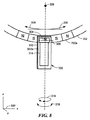
図1を参照すると、一例の磁場センサ10は、例えばギア歯22a、22b、22cなどの強磁性ギア歯を有するギア22に応答する。ギア22は、磁場センサ10が応答し得る「強磁性対象物体」又は単なる「対象」の一種にすぎないことを理解すべきである。
Referring to FIG. 1, an example
磁場センサ10は、電子回路16に結合された磁場検知素子12を備える。磁場検知素子12及び電子回路16は、基板14上(すなわち、基板14内に統合されるか又は基板14上)に配置され得る。明確にするために、磁場検知素子12は誇張されたサイズでホール素子として示され、基板14の平面から離れて回転する。さらに、明確にするために、ホール素子12は基板14の上部に示されるが、ホール素子は通常、統合された回路の基板の面上又は面内に配置されると理解される。
The
磁場センサ10は、磁石18(例えば、永久磁石又はハード材強磁性体)を備え得る。磁石18は、磁場を生成するように構成され、磁場は、磁場検知素子12の場所において全体的に軸24に沿って方向づけられ、磁場センサ10に対するギア歯22a、22b、22cの位置に応じた方向及び振幅変化に依存する。しかしながら、磁石18の表面における磁場の構造は、コア20に起因してより複雑化し得る。
The
電子回路16は、(図示しない)出力信号を生成するように構成される。ギアが動いていないときに、出力信号は、磁場センサ10がギア歯の上にあるのかギアの谷にあるのかを示す。したがって、磁場センサ10は「エッジ検出器」と対比される「歯検出器」として参照されることもある。ギアが回転しているときに、出力信号は、エッジレート又はギアの回転速度の周波数表示を有する。出力信号のエッジ又は状態の遷移は、磁場センサを通り過ぎるギア歯のエッジの位置を特定するために用いられ得る。
The
磁石18は、磁石18内に配置されたソフト材強磁性体に含まれる中央コア20を備えることができる。コアを有する磁石の一例は、2001年8月21日発行の「Magnet Structure(磁石構造)」という名称の米国特許第6,278,269号に記述され、この特許は本発明の譲受人に譲渡され、記載内容の全体が本明細書に援用される。米国特許第6,278,269号に記載されるように、コア20を有する磁石18によって提供される磁極構成は、ギア22の谷が磁場センサ10に近接したときに、コア20の表面上(例えば、示されるようにコアの左側)のいくつかのポイントにおいて、磁場の磁束密度のベースフィールド(又はベースライン)を低下させる。磁場検知素子12における所定のベースライン(例えば、約+/600ガウスの範囲内)、及び結果として生じるゼロに近い差動磁場信号12a、12b(すなわちアナログ差動近接信号)は、適切な設計で得られ得る。
The
これに対して、ギア22のギア歯が磁場検知素子12に近接すると、磁場検知素子12は、より高い磁場を感じてより高い値の差動磁場信号12a、12bを生成する。上記の通り、ベースライン磁場とより高い磁場との間の差は、磁場センサ10の最終的な正確性に関連する。
On the other hand, when the gear teeth of the
磁場センサ10がギア22の谷に近接したときに生じ得るベースライン磁場は、ギア22と磁場センサ10との間の空隙が変化したとしても、変化が小さく比較的低いままである。実質的に空隙とは無関係な低いベースラインのこの有利な結果は、コア20の動作によって得られ、これによって、特に磁場検知素子12がギア22の谷に近接するときに、磁場検知素子12に近接するコア20の表面(すなわち図示されるように左側)に反対磁極が現れるという結果をもたらす。この効果は、1998年7月14日発行の「Hall−Effect Ferromagnetic−Article−Proximity Sensor(ホール効果鉄物品近接センサ)」という名称の米国特許第5,781,005号にも記述され、この特許は本発明の譲受人に譲渡され、記載内容の全体が本明細書に援用される。
The baseline magnetic field that can occur when the
磁場センサがギアの谷に近接したときに生じる上記の低いベースラインは、ギア歯の存在をギアの谷と識別する電子回路16の性能を強化するという結果をもたらす。
ベースライン磁場は比較的小さく、これにより磁場センサ10がギア22の谷に近接したときに温度によって生じる回路変動の影響を少なくすることができるので、上記の低いベースラインは、温度効果をより容易に補償する性能も提供する。本質的に、(ゼロ付近の)エラーの増加は小さいので、回路におけるエラーは、ベースライン磁場レベル又はベースライン磁場範囲の近くで十分に修正され得る。したがって、温度又は湿度などの動作状態によるシステムのノイズ又はエラーが少ないので、歯を谷と区別するために用いられる磁場閾値は、正確性を維持している間は小さく設定され得る。
The low baseline described above that occurs when the magnetic field sensor is close to the gear trough results in enhanced performance of the
The low baseline makes the temperature effect easier because the baseline magnetic field is relatively small, which can reduce the effects of circuit variations caused by temperature when the
上記に記載された、コア20を有する磁石18によって提供される磁場は、磁場センサ10の正確性を向上させるという結果をもたらす。例えば、低いベースラインによれば、磁場センサ10の正確性を犠牲にすることなく、ユニット間の機械的位置合わせのばらつきによって磁場検知素子12が磁石18の中心から静的に多少ずれることを許容する。正確性については、上記で議論される。
The magnetic field provided by the
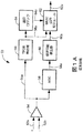
図1Aを参照すると、例示の従来技術の電子回路50は、図1の電子回路16と同一又は同様であり得る。電子回路50は、図1の磁場検知素子12によって生成された差動信号12a、12bと同一又は同様であり得る差動信号52a、52bを受信するために結合された増幅器54を含み得る。増幅器54は、増幅された信号54aを生成するように構成され、いくつかの実施形態では、増幅された信号54aは、TPOS検出チャネル及び精密回転検出チャネルという2個のチャネルに分割され得る。
Referring to FIG. 1A, an exemplary prior art
真のパワーオン状態(TOPS:true power on state)チャネルにおいて、TPOS検出器56は、増幅された信号54aを受信するために結合され、TPOS出力信号56aを生成するように構成され得る。ある実施形態では、TPOS検出器56は、増幅された信号54aを固定された(及び調整された)閾値と比較するように構成された(図示されない)比較器を備え得る。これらの実施形態では、TPOS出力信号56aは、2個の状態の2進信号であってもよく、高状態はギア歯が図1の磁場センサ10に近接していることを示し、低状態はギアの谷が磁場センサ10に近接していることを示し、又はこの逆であってもよい。
In a true power on state (TOPS) channel,
精密回転検出チャネルにおいて、自動利得制御(AGC)58は、増幅された信号54aを受信するために結合され、利得制御信号58aを生成するように構成され得る。精密回転検出器60は、利得制御信号58aを受信するために結合され、精密回転検出器出力信号60aを生成するように構成され得る。TPOS出力信号56aと同様に、精密回転検出器出力信号60aは、2個の状態の2進信号であってもよく、高状態はギア歯が図1の磁場センサ10に近接していることを示し、低状態はギアの谷が磁場センサ10に近接していることを示し、又はこの逆であってもよい。したがって、TPOS検出器56及び精密回転検出器60の両者は、「歯検出器」であり得る。しかしながら、精密回転検出チャネルはAGC58を使用し、AGC58は、ギア22が回転していないときに望ましくない利得を安定させ、ギア22が回転し始めたら、利得が不正確でありかつ正確な回転検出を十分に精度高く行えない期間を生じさせるということを理解すべきである。たとえAGC58が使用されなかったとしても、精密回転検出器60は、ギア22が回転しているときにのみ適切に更新される内部閾値を使用する。しかしながら、他の実施形態においては、閾値は電子回路50の外部から供給され得る。
In the precision rotation detect channel, an automatic gain control (AGC) 58 may be coupled to receive the amplified
代替の実施形態においては、精密回転検出器60は、特にギアが動いていないときに磁場センサ12がギア歯又はギア谷に近接しているかを特定することができないが、磁場センサ10を通り過ぎるギア歯のエッジを検知することが可能な「エッジ検出器」であり得る。
In an alternative embodiment, the
精密回転検出器、例えば精密回転検出器60は、様々な形態を有することができる。いくつかの形態は上記の米国特許第6,525,531号に記載される。しかしながら、2個以上の磁場検知素子を含むものなど、他の形態の精密回転検出器も知られている。
The precision rotation detector, eg,
一般的に、上記の議論から、TPOS出力信号56aは、たとえギア、例えば図1のギア22が静止しているときにも、磁場検知素子12がギア歯又はギアの谷に近接しているかを示すことが理解される。しかしながら、TPOS検出器56はいくつかの実施形態において電源投入時に限定された調整を有する固定の閾値を使用するので、TPOS出力信号56aにおけるエッジ配置の変動が、これらに限定されるものではないが、温度変化及び磁場検知素子12とギア22との間の空隙の変化を含む様々な要因に起因して生じ得る。
In general, from the discussion above, the
固定の閾値を用いるTPOS検出器56とは異なり、精密回転検出器60は、ギア歯の物理的な位置に対する精密回転検出器出力信号60aのエッジ配置の正確性を高めた精密回転検出器出力信号60aを供給するために断続的に閾値の調整を行う。上記の通り、これらの調整は、部分的には、最初に電源が投入されたとき又はギア22が最初に回転し始めたときに精密回転検出器の正確性を低くする。
Unlike the
TPOS検出器56及び精密回転検出器60が共通の基板に統合されたいくつかの実施形態において、マルチプレクサ/出力モジュール62は、TPOS出力信号56a及び精密回転検出器出力信号60aを受信するために結合され得る。選択ロジック64は、マルチプレクサ/出力モジュール62によって受信される選択信号64aを供給し得る。選択信号64aの状態に応じて、マルチプレクサ/出力モジュール62は、TPOS出力信号56a又は精密回転検出器出力信号60aのうちの選択された一方を示す出力信号62aを生成するように構成される。出力信号62aは、これらに限定されるものではないが、SENTフォーマット、I2Cフォーマット、PWMフォーマット、又はTPOS出力信号56a及び精密回転検出器出力信号60aで元々用いられる二状態フォーマット、を含む様々な信号形態で供給され得る。
In some embodiments in which
いくつかの実施形態において、選択ロジック64は、ギア22が回転し始めた後TPOS出力信号56aによって示された所定の時間はTPOS出力信号56aを表す出力信号62aを選択する。その後、選択ロジック64は、精密回転検出器出力信号60aを表す出力信号62aを選択する。
In some embodiments, the
図2を参照すると、他の例の従来技術の磁場センサ200は、例えばギア歯214a、214b、214cなどのギア歯を有するギア214に応答する。磁場センサ200は、電子回路210に結合された3個の磁場検知素子202、204、206を備える。いくつかの実施形態において、磁場検知素子202、204は、軸216に直交する方向に約1.5ミリメートルから約3.0ミリメートルの距離だけ離れており、磁場検知素子206は、磁場検知素子202、204の中間に配置される。
Referring to FIG. 2, another example prior art
3個の磁場検知素子202、204、206及び電子回路210は、基板208上(すなわち基板208内に統合されるか又は基板208上)に配置され得る。明確にするために、磁場検知素子202、204、206は誇張されたサイズでホール素子として示され、基板208の平面から離れて回転する。さらに、明確にするために、ホール素子202、204、206は基板208の上部に示されるが、ホール素子は通常、統合された回路の基板の面上又は面内に配置されると理解される。
The three magnetic
磁場センサ200は、磁石212も備え得る。磁石212は、磁場を生成するように構成され、磁場は、磁場検知素子202、204、206の場所において全体的に軸216に沿って方向づけられる。
The
電子回路210は、(図示しない)出力信号を生成するように構成される。例示の電子回路210は、図2Aと合わせて以下に記載される。ここでは電子回路は信号の相違を生成するというだけで十分である。したがって、磁場センサ200は、エッジ検出器であり、歯検出器ではないということが理解される。
ギア214が回転しているときに、出力信号は、ギア214の回転速度を表し、ギア歯のエッジの位置も表す。磁場センサ200は、TPOS機能を提供することはできず、ギア214が静止しているときに、磁場検知素子202、204、206がギア歯又はギア214の谷に近接しているかを特定することができない。
When the
磁石212は、単一の材料によって構成されてもよく、図1に合わせて図示され説明された中央コアを備えなくてもよい。しかしながら、他の実施形態においては、磁石212は、図1に合わせて図示され説明された中央コアと同一又は同様の中央コアを備え得る。
The
磁場センサ200は、3個の差動信号202a、202bと、204a、204bと、206a、206bとをそれぞれ生成するために3個の磁場検知素子202、204、206を使用する。単純な磁石212は、コアを有する磁石の低いベースラインを提供しないが、上記の差動信号の差は、低いベースラインの効果をもたらす。本質的には、3個の磁場検知素子202、204、206に同じ磁場がかかったときに、上記の差動信号の相違が電気信号においてゼロになる。
The
図2Aを参照すると、例示の従来技術の電子回路250は、図2の電子回路210と同一又は同様であり得る。電子回路250は、差動信号252a、252bと、254a、254bと、256a、256bとをそれぞれ受信するために結合された増幅器258、260、262を含み得る。差動信号252a、252bと、254a、254bと、256a、256bとは、図2の磁場検知素子202、204、206によってそれぞれ生成された差動信号202a、202bと、204a、204bと、206a、206bと同一又は同様であり得る。増幅器258、260、262はそれぞれ、増幅された信号258a、260a、262aを生成するように構成される。
Referring to FIG. 2A, the exemplary prior art
増幅された信号258a、260aは、第1の差異信号264aを生成するように構成された第1の差異モジュール264によって受信される。増幅された信号260a、262aは、第2の差異信号266aを生成するように構成された第2の差異モジュール266によって受信される。
The amplified
電子回路250は、図1Aに合わせて説明された2個の精密回転検出チャネルを備える。AGC270、276は、図1AのAGC56と同一又は同様であり得る。精密回転検出器272、278は、図1Aの精密回転検出器60と同一又は同様であり得る。精密回転検出器272は、精密回転検出器出力信号272aを生成することができ、精密回転検出器278は、精密回転検出器出力信号278aを生成することができる。精密回転検出器出力信号272a、278aは、図1Aの精密回転検出器出力信号60aと同一又は同様であり得る。
The
速度及び方向モジュール274は、精密回転検出器出力信号272a、278aを受信するために結合され得る。
精密回転検出器出力信号272a、278aは、ギア214の回転方向によって決定される相対位相であることは明らかである。精密回転検出器出力信号272a、278aの状態遷移レートはギア214の回転速度を表すことも明らかである。
Velocity and
It will be appreciated that the precision rotation
速度及び方向モジュールは、ギア214の回転速度又は回転方向の少なくとも一方を表し得る出力信号を生成するように構成される。いくつかの実施形態において、出力信号62aは、回転速度及び回転方向の両方を表す。
The speed and direction module is configured to generate an output signal that may represent a rotational speed or a rotational direction of the
図3を参照すると、磁場センサ300は、例えばギア歯322a、322b、322cなどのギア歯を有するギア322に応答する。ギア322は、強磁性ギア、すなわち強磁性歯を有する強磁性対象物体、また強磁性対象であり得、本明細書において対象特性として参照される。磁場センサ300は、主面302aを有する基板302を備え得る。
Referring to FIG. 3, the
磁場センサ300は、基板302の主面302aに配置された磁場検知素子304を備え得る。磁場検知素子304のさらなる詳細は以下に記載される。しかしながら、ここでは磁場検知素子304が少なくとも2個の磁気抵抗素子を備え得るというだけで十分である。
The
磁場検知素子304は、基板302の主面302aに配置された電子回路314に、又は電子回路314内に結合され得る。
磁場センサ300は、磁石332も備えることもできる。磁石332は、磁場を生成するように構成され、磁場は、磁場検知素子304の場所において全体的に軸308に沿って方向づけられ、基板302の主面302aに全体的に平行である。
The magnetic
The
磁場検知素子304は、基板302の主面302aに平行なそれぞれの最大応答軸を有する。いくつかの実施形態において、最大応答軸は互いに平行である。いくつかの実施形態において、最大応答軸は、軸308に実質的に平行である。いくつかの実施形態において、最大応答軸は、軸308に実質的に直交する。
The magnetic
基板の主面302aに直交するライン(すなわちページ内へのライン)は、磁石332と交差し、ギア322と交差しない。さらに、いくつかの実施形態において、磁場検知素子304は、磁場検知素子304間の(すなわち通過する)軸(例えば軸308)がギア322と交差しない位置に配置される。いくつかの実施形態において、磁場検知素子304間の(すなわち通過する)軸(例えば軸308)は、ギア322の移動方向例えば326に対する接線330に実質的に平行である。
The line orthogonal to the
示される実施形態において、磁石332の北(N)極と南(S)極との間のラインは、基板302の主面302aに対して実質的に平行であり、2個の磁場検知素子304、306間の(すなわち通過する)軸(例えば軸308)に対して実質的に平行である。いくつかの実施形態において、磁石332のN極とS極との間のラインは、ギア322に交差せず、ギア322の方向に向いていない。
In the illustrated embodiment, the line between the north (N) and south (S) poles of the
電子回路314は、(図示されない)出力信号を生成するように構成される。例示の電子回路314は、図26と合わせて以下に記載される。ここでは電子回路314は信号の相違及び信号の合計を生成するというだけで十分である。したがって、磁場センサ300は、エッジ検出器及び歯検出器の両方であるということが明らかである。
ギア322が回転しているときに、出力信号は、ギア322の回転速度を表し、ギア歯のエッジの位置も表す。磁場センサ300は、歯検出(例えばTPOS)機能を提供することができ、ギア322が静止しているときに、磁場検知素子304がギア歯又はギア322の谷に近接しているかを特定することができる。
When the
磁石332は、単一の材料によって構成されてもよく、図1と合わせて図示され説明された中央コアを備えなくてもよい。しかしながら、他の実施形態においては、磁石332は、図1と合わせて図示され説明された中央コアと同一又は同様の中央コアを備え得る。このようなコアは軸324と整列された軸を有し得る。
磁場センサ300は、性能を低下させることなく、図示される位置から離れて方向316において次の位置へ360度回転し得る。しかしながら、中間回転は性能の低下を生じ得る。
The
磁場センサ300は、実質的に性能を低下させることなく、ライン324に沿った任意の場所の回転中心に対して矢印318の方向に+/−20度の範囲で回転し得る。
いくつかの実施形態において、磁場検知素子304は、磁気抵抗素子である。
The
In some embodiments, the magnetic
図4を参照すると、図3と同様の参照符号が付された同様の要素が示され、磁場センサ300は、基板302、及び基板302上の磁場検知素子304がギア322に重なる配置で図示される。基板の面302aに直交し磁場検知素子304を通過するラインは、ギア322に交差する。
Referring to FIG. 4, similar elements labeled the same as in FIG. 3 are shown and the
図5を参照すると、図3と同様の参照符号が付された同様の要素が示され、磁場センサ300は、図3に示された配置と比べるとx軸の周りに90度ページの外側又はページの内側へ回転した配置で図示される。磁場検知素子304はギア322に近接したまま配置される。
Referring to FIG. 5, similar elements with similar reference numbers to FIG. 3 are shown, and the
図6を参照すると、図3と同様の参照符号が付された同様の要素が示され、磁場センサ600は、図3の磁場センサ300と同様であるが、磁場センサ600は、異なる磁石602を有する。磁場センサ600は、磁石602の北(N)極と南(S)極との間のラインが基板302の主面302aに対して実質的に平行であるが、磁場検知素子間の(すなわち通過する)軸(例えば軸308)に対して実質的に直交する、異なる磁石602を有する。いくつかの実施形態において、磁石602のN極とS極との間のラインは、ギア322の方向に向く。
Referring to FIG. 6, similar elements with similar reference numbers to FIG. 3 are shown, and the
いくつかの実施形態において、磁石602は、図1と合わせて説明されたようなコアを有さない単純な磁石である。他の実施形態において、磁石602は、ライン324に沿った軸を有するコアを有する。
In some embodiments, the
上記に図示され説明された磁場センサは、ギア又はカムの形態の強磁性対象物体の動きを検知するために示された。しかしながら、以下に記載される図7〜9は、リング磁石の動きを検知するための同一又は同様の磁場センサを示す。エッジ検出器、歯検出器、及びTPOS機能に関して上記でなされたコメントは、リング磁石を検知する際に同様に適用される。 The magnetic field sensor shown and described above has been shown to detect the movement of a ferromagnetic target object in the form of a gear or cam. However, FIGS. 7-9, described below, show the same or similar magnetic field sensors for sensing the movement of the ring magnet. The comments made above regarding edge detectors, tooth detectors, and TPOS functionality apply as well in detecting ring magnets.
図7を参照すると、図3〜6と同様の参照符号が付された同様の要素が示され、磁場センサ700は、図3の磁場センサ300と同様である。しかしながら、磁場センサ700は、内部磁石を有さない。その代わり、磁場センサ700は、リング磁石702の例えば702aの通過する磁区に応答する。
Referring to FIG. 7, similar elements labeled the same as in FIGS. 3-6 are shown, and the
いくつかの実施形態において、リング磁石702の磁区は、ページに平行に分極される。いくつかの他の実施形態において、リング磁石702の磁区はページに直交して分極される。
In some embodiments, the magnetic domains of
図8を参照すると、図3〜7と同様の参照符号が付された同様の要素が示され、磁場センサ700は、基板302、及び基板302上の磁場検知素子304がリング磁石702に重なる配置で図示される。磁場センサ700は、磁場検知素子304がなおリング磁石702の例えば702aの磁区に重なるようにy軸の周りに180度回転し得ることは明らかである。基板302の面302aに直交し磁場検知素子304を通過するラインは、リング磁石702に交差する。
Referring to FIG. 8, similar elements labeled the same as in FIGS. 3-7 are shown, in which the
図9を参照すると、図3〜8と同様の参照符号が付された同様の要素が示され、磁場センサ700は、図5に示された配置と比べるとx軸の周りに90度ページの外側又はページの内側へ回転した配置で図示される。磁場検知素子304はリング磁石702に近接したまま配置される。
Referring to FIG. 9, similar elements with similar reference numbers to FIGS. 3-8 are shown, and the
以下の図では、符号A、B、C、D、A1、A2、B1、B2、C1、C2、D1、D2、P1、P2、P3、P4は、磁気抵抗素子を表す符号として示される。これらの符号は、同様の図面における同様に符合間の論理関係を表すことを理解すべきである。しかしながら、これらの符号は、1図面において示された磁気抵抗素子が他の図面において同じ符号が付されたものと同じ磁気抵抗素子であることを意味しない。 In the following figures, the symbols A, B, C, D, A1, A2, B1, B2, C1, C2, D1, D2, P1, P2, P3, P4 are shown as the symbols representing the magnetoresistive elements. It should be understood that these reference numerals likewise represent logical relationships between the reference numerals in similar drawings. However, these reference numbers do not mean that the magnetoresistive element shown in one drawing is the same magnetoresistive element given the same reference numeral in the other drawings.
同様に、以下の図面では、符号V1、V2は、2個の信号を表す符号として示される。これらの符号は、同様の図面における同様の符合間の論理関係を表すことを理解すべきである。しかしながら、これらの符号は、1図面において示された信号が他の図面において同じ符号が付されたものと同じ信号であることを意味しない。 Similarly, in the following drawings, the symbols V1 and V2 are shown as symbols representing two signals. It should be understood that these reference numerals represent logical relationships between similar reference numerals in similar drawings. However, these reference numbers do not mean that the signals shown in one figure are the same signals given the same reference numbers in the other figures.
同様に、以下の図面では、符号R1、R2は、2個の固定抵抗を表す符号として示される。これらの符号は、同様の図面における同様の符合間の論理関係を表すことを理解すべきである。しかしながら、これらの符号は、1図面において示された抵抗が他の図面において同じ符号が付されたものと同じ抵抗であることを意味しない。 Similarly, in the following drawings, the symbols R1 and R2 are shown as symbols representing two fixed resistors. It should be understood that these reference numerals represent logical relationships between similar reference numerals in similar drawings. However, these reference numbers do not mean that the resistances shown in one drawing are the same as those given the same reference numbers in the other drawings.
図10を参照すると、磁場センサ1000は、面1002aを有する基板1002を備えることができ、面1002aは、基板1002の2個の平行な主面のうちの一方である。
Referring to FIG. 10, the
2個の磁気抵抗素子1004、1006(本明細書では磁気抵抗素子A及びBとしても参照される)は、軸1010に沿って面1002a上に配置され得る。2個の磁気抵抗素子1004、1006(A、B)は、基板1002の面1002a上又は面1002a内に配置された電子回路1008の一部であるか又は電子回路1008に結合され得る。2個の磁気抵抗素子1004、1006(A、B)は、図3〜9の磁場検知素子304と同一又は同様であり得る。軸1010は、図3〜9の軸308と平行であり得る。
Two
磁気抵抗素子、例えば1004、1006(A、B)は、C形状(又は反転C形状)を有する「ヨーク」と呼ばれる形態で本明細書の全ての実施形態で示される。いくつかの実施形態において、ヨークは、軸1010に実質的に直交する最も長いヨーク軸を有することができる。ヨーク形状の利点は知られている。本明細書の実施形態で用いられる他の磁気抵抗素子は、例えば、ライン状、ポリライン状、又は矩形状などの他の形状を有し得ることが理解される。
Magnetoresistive elements, such as 1004, 1006 (A, B) are shown in all embodiments herein in a form called a "yoke" having a C-shape (or inverted C-shape). In some embodiments, the yoke can have the longest yoke axis that is substantially orthogonal to
磁気抵抗素子1004、1006(A、B)の最大応答軸は、軸1010に沿って同じ方向に軸1010と平行であり得る。軸1010に平行な最大応答軸を有する磁気抵抗素子1004、1006(A、B)もまた、基板1002の平面において(かつ基板1002の平面外において)他の角度で磁場に応答することが理解される。磁気抵抗素子1004、1006(A、B)が軸1010に平行ではない(かつ最も長いヨーク軸に直交しない)他の角度において磁場に応答する角度は、軸1010上の他の角度における磁場の幾何放射の大きさによって決定される。したがって、「放射磁場」という用語は、以下、この放射を説明するために使用される。
The maximum response axes of
他のいくつかの実施形態において、磁気抵抗素子1004、1006のヨーク形状は、最も長いヨーク軸が軸1010に直交しないように回転することができ、磁気抵抗素子1004、1006(A、B)が軸1010に平行ではない他の角度において磁場に応答する角度は、ヨーク形状の最も長い軸に直交する軸上の他の角度における磁場の幾何放射の大きさによって決められる。これは本明細書において放射磁場としても参照される。
In some other embodiments, the yoke shape of the
磁場センサ1000は、幅1014をもつ特徴物、例えば1012aを有する強磁性対象物体1012の動きに応答する。強磁性対象物体1012は、図3〜6のギア322と同一又は同様であってもよく、又は図7〜9のリング磁石702と同一又は同様であってもよい。例えば1012aの特徴物は、図3〜6の例えば322aのギア歯と同一又は同様であってもよく、又は図7〜9のリング磁石702の例えば702aの磁区と同一又は同様であってもよい。
The
磁場センサ1000は、図3〜5の磁場センサ300、図6の磁場センサ600、及び図7〜9の磁場センサ700と同一又は同様であってもよい。しかしながら、磁場センサ1000は、上記の図5及び図9と合わせて説明された回転位置では図示されない。それにもかかわらず、磁場センサ1000は、同様にページの内側又は外側に回転することができる。
The
いくつかの実施形態において、2個の磁気抵抗素子1004、1006(A、B)は、例えば強磁性ギアのギア歯又は強磁性リング磁石の磁区などの対象特徴物1012aの幅1014の約1/2から約1.5倍の間の間隔1016を有する。いくつかの他の実施形態において、2個の磁気抵抗素子1004、1006(A、B)は、対象特徴物1012aの幅1014の約1/2から約2倍の間の間隔1016を有する。しかしながら、他の実施形態においては、間隔1016は、例えば、幅1014の百分の一のように幅1014の半分よりももっと小さく、又は幅1014の2倍よりも大きい。
In some embodiments, the two
以下の例で用いられるいくつかの実施形態において、間隔1016は、例えば強磁性ギアのギア歯又は強磁性リング磁石の磁区などの対象特徴物1012aの幅1014と略等しい。
In some embodiments used in the examples below, the
動作中において、2個の磁気抵抗素子1004、1006(A、B)は、2個の出力信号を生成することができる。以下に示され説明される図面は、2個の磁場検知素子1004、1006が2個の出力信号を生成し得る様々な方法を表す。
In operation, the two
例示として2個の磁気抵抗素子1004、1006間の間隔1016と等しい幅1014を有する対象特徴物1012aを用いると、対象特徴物1012aが2個の磁気抵抗素子1004、1006の中央(すなわちこれらの間)にあるときに、対象特徴物1012aの中央の片側上のいかなる磁気抵抗素子(例えば1004(A))にも軸1010に沿って一方向に向けられた放射磁場がかかり、対象特徴物1012aの中央の反対側上のいかなる磁気抵抗素子(例えば1006(B))にも反対方向に向けられた放射磁場がかかることが示され得る。
As an example, using a
したがって、対象特徴物1012aが2個の磁気抵抗素子1004、1006の中央にあるときに、対象特徴物1012aの中央の片側上のいかなる磁気抵抗素子(例えば1004(A))も一方向に抵抗が変化し、対象特徴物1012aの中央の反対側上のいかなる磁気抵抗素子(例えば1006(B))も反対方向に抵抗が変化する。
Therefore, when the
これに対して、対象特徴物1012aのエッジが2個の磁気抵抗素子1004、1006の中央(すなわちこれらの間)にあるときには、2個の磁気抵抗素子1004、1006(A、B)に軸1010に沿って同じ方向に向けられた放射磁場がかかることが示され得る。したがって、2個の磁気抵抗素子1004、1006(A、B)の両方の抵抗は同じ方向に変化する。
On the other hand, when the edge of the
図3の磁石332のような磁石は図示されないが、いくつかの実施形態において、磁場センサ1000は磁石を備え得ることが理解される。
図11を参照すると、図10と同様の要素が同様の参照符号とともに示され、2個の磁気抵抗素子1004、1006(A、B)は、それぞれの電流源1102、1104とグラウンドとの間に結合される。2個の出力信号1106=V1と1108=V2が生じる。以下、上記の説明を明確にするために符号V1及びV2が用いられる。
A magnet, such as
Referring to FIG. 11, elements similar to those of FIG. 10 are shown with like reference numerals, and two
2個の出力信号V1、V2の処理は図26と合わせてより詳細に説明される。しかしながら、ここでは、この配置において、図10の対象特徴物1012aが2個の磁気抵抗素子1004、1006(A、B)の中央にあるときに、2個の出力信号V1、V2の差V1−V2が(正又は負の)最大の瞬時値をとるというだけで十分である。上記の通り、対象特徴物1012aは、図3のギア322の例えば322aの歯(又は代替では谷)、又は図7のリング磁石702の例えば702aの磁区(北又は代替で南)であり得る。したがって、差V1−V2は、歯の近接又は磁区の近接を表し、それゆえ強磁性対象物体の「特徴物」を表す。
The processing of the two output signals V1 and V2 will be described in more detail in conjunction with FIG. However, here, in this arrangement, when the
これに対して、2個の磁気抵抗素子1004、1006(A、B)が図10の対象特徴物1012aのエッジ1012aの反対側にあるときに、2個の出力信号V1、V2の和V1+V2は、(正又は負の)最大の瞬時値をとる。したがって、和V1+V2はエッジの近接を表し、それゆえ強磁性対象物体の「エッジ」を表す。
On the other hand, when the two
2個の信号V1、V2の差V1−V2及び2個の信号V1、V2の和V1+V2の両方を用いる磁場センサは、それぞれ歯検出器及びエッジ検出器の両方として動作することができる。いくつかの実施形態において、歯検出器の性能により、図示のように結合された2個の磁気抵抗素子1004、1006を用いる磁場センサは、真のパワーオン状態(TPOS)機能を備えて動作することが可能となる。
A magnetic field sensor using both the difference V1-V2 of the two signals V1, V2 and the sum V1 + V2 of the two signals V1, V2 can operate as both a tooth detector and an edge detector, respectively. In some embodiments, due to the performance of the tooth detector, a magnetic field sensor using two
以下の図27、28と合わせて説明するように、ここでの、及び以下の図面における2個の信号V1、V2は、移動する強磁性物体の速度及び方向の両方を決定するために用いられる。以下の議論から2個の信号の和V1+V2は2個の信号の差V1−V2から90度離れていることも明らかになるはずである。 As explained in conjunction with FIGS. 27 and 28 below, the two signals V1, V2 here and in the following figures are used to determine both the velocity and the direction of a moving ferromagnetic object. . It should also be apparent from the following discussion that the sum of the two signals, V1 + V2, is 90 degrees away from the difference of the two signals, V1-V2.
図12を参照すると、図10と同様の要素が同様の参照符号とともに示され、2個の磁気抵抗素子1004、1006(A、B)は、本明細書において抵抗R1、R2としても参照される固定抵抗1202、1204を有するブリッジ配置1200内に結合される。いくつかの実施形態において、固定抵抗1202、1204(R1、R2)は、例えば2010年8月17日に発行され、本出願の譲受人に譲渡され、記載内容の全体が本明細書に援用される米国特許第7,777,607号に記載される磁気抵抗素子のようないくつかの層を有する磁気不感要素(又は感度が低い要素)であり得る。このような磁気不感要素は、2個の磁気抵抗素子1004、1006(A、B)と同一の温度係数を有する傾向にあり、したがって、ブリッジ1200は実質的に温度変化に不感とすることができる。
12, elements similar to those of FIG. 10 are shown with like reference numerals, and the two
ブリッジ1200は、電圧源1206によって電源を供給され得る。2個の出力信号1208=V1、1210=V2が生じる。以下、上記の説明を明確にするために符号V1及びV2が用いられる。
The
ブリッジ配置においてはしばしば、2個の出力信号V1、V2は、1個の差動信号V1、V2として扱われる。しかしながら、ここでは、2個の出力信号V1、V2は、別々に扱われる。 Often in a bridge arrangement, the two output signals V1, V2 are treated as one differential signal V1, V2. However, here the two output signals V1, V2 are treated separately.
2個の出力信号V1、V2の処理は、以下の図26と合わせて詳細に説明される。しかしながら、ここでは、この配置において、図10の対象特徴物1012aが2個の磁気抵抗素子1004、1006(A、B)の中央にあるときに、2個の出力信号V1、V2の差V1−V2が(正又は負の)最大の瞬時値をとるというだけで十分である。上記の通り、対象特徴物1012aは、図3のギア322の例えば322aの歯(又は代替では谷)、又は図7のリング磁石702の例えば702aの磁区(北又は代替で南)であり得る。したがって、差V1−V2は、歯の近接又は磁区の近接を表し、それゆえ強磁性対象物体の「特徴物」を表す。
The processing of the two output signals V1 and V2 will be described in detail in conjunction with FIG. 26 below. However, here, in this arrangement, when the
これに対して、2個の磁気抵抗素子1004、1006(A、B)が図10の対象特徴物1012aのエッジ1012aの反対側にあるときに、2個の出力信号V1、V2の和V1+V2は、(正又は負の)最大の瞬時値をとる。したがって、和V1+V2はエッジの近接を表し、それゆえ強磁性対象物体の「エッジ」を表す。
On the other hand, when the two
2個の信号V1、V2の差V1−V2及び2個の信号V1、V2の和V1+V2の両方を用いる磁場センサは、それぞれ歯検出器及びエッジ検出器の両方として動作することができる。いくつかの実施形態において、歯検出器の性能により、図示のように結合された2個の磁気抵抗素子1004、1006(A、B)を用いる磁場センサは、真のパワーオン状態(TPOS)機能を備えて動作することが可能となる。
A magnetic field sensor using both the difference V1-V2 of the two signals V1, V2 and the sum V1 + V2 of the two signals V1, V2 can operate as both a tooth detector and an edge detector, respectively. In some embodiments, due to the performance of the tooth detector, a magnetic field sensor using two
図13を参照すると、図10と同様の要素が同様の参照符号とともに示され、2個の磁気抵抗素子1004、1006(A、B)は、(本明細書においてR1、R2としても参照される)固定抵抗1302、1304を有するブリッジ配置1300内に結合される。いくつかの実施形態において、固定抵抗1302、1304は、例えば2010年8月17日発行の米国特許第7,777,607号に記載されている磁気抵抗素子のようないくつかの層を有する磁気不感要素であり得る。
13, elements similar to those of FIG. 10 are shown with like reference numerals, and the two
ブリッジ1300は、電圧源1306によって電源を供給され得る。2個の出力信号1308=V1、1310=V2が生じる。以下、上記の説明を明確にするために符号V1及びV2が用いられる。
ブリッジ配置においてはしばしば、2個の出力信号V1、V2は、1個の差動信号V1、V2として扱われる。しかしながら、ここでは、2個の出力信号V1、V2は、別々に扱われる。 Often in a bridge arrangement, the two output signals V1, V2 are treated as one differential signal V1, V2. However, here the two output signals V1, V2 are treated separately.
2個の出力信号V1、V2の処理は、以下の図26と合わせて詳細に説明される。しかしながら、ここでは、この配置において、図10の対象特徴物1012aが2個の磁気抵抗素子1004、1006(A、B)の中央にあるときに、2個の出力信号V1、V2の和V1+V2が(正又は負の)最大の瞬時値をとるというだけで十分である。上記の通り、対象特徴物1012aは、図3のギア322の例えば322aの歯(又は代替では谷)、又は図7のリング磁石702の例えば702aの磁区(北又は代替で南)であり得る。したがって、和V1+V2は、歯の近接又は磁区の近接を表し、それゆえ強磁性対象物体の「特徴物」を表す。
The processing of the two output signals V1 and V2 will be described in detail in conjunction with FIG. 26 below. However, here, in this arrangement, when the
これに対して、2個の磁気抵抗素子1004、1006(A、B)が図10の対象特徴物1012aのエッジ1012aの反対側にあるときに、2個の出力信号V1、V2の差V1−V2は、(正又は負の)最大の瞬時値をとる。したがって、差V1−V2はエッジの近接を表し、それゆえ強磁性対象物体の「エッジ」を表す。
On the other hand, when the two
2個の信号V1、V2の和V1+V2及び2個の信号V1、V2の差V1−V2の両方を用いる磁場センサは、それぞれ歯検出器及びエッジ検出器の両方として動作することができる。いくつかの実施形態において、歯検出器の性能により、図示のように結合された2個の磁気抵抗素子1004、1006(A、B)を用いる磁場センサは、真のパワーオン状態(TPOS)機能を備えて動作することが可能となる。
A magnetic field sensor using both the sum V1 + V2 of the two signals V1, V2 and the difference V1-V2 of the two signals V1, V2 can act as both a tooth detector and an edge detector, respectively. In some embodiments, due to the performance of the tooth detector, a magnetic field sensor using two
上記の図12及び図13は、特にブリッジ配置について示したが、明らかになるはずである他のブリッジ配置の可能性もある。例えば、磁場検知素子1004、1006は、位置が置き換わってもよい。
Although FIGS. 12 and 13 above specifically show a bridge arrangement, there are other bridge arrangement possibilities that should be apparent. For example, the positions of the magnetic
図14を参照すると、磁場センサ1400は、面1402aを有する基板1402を備えることができ、面1402aは、基板1402の2個の平行な主面のうちの一方である。
Referring to FIG. 14, the
4個の磁気抵抗素子1404、1406、1408、1410(本明細書ではA、B、C、Dとしても参照される)は、面1402a上に配置され得る。4個の磁気抵抗素子1404、1406、1408、1410(A、B、C、D)は、基板1412の面1402a上又は面1402a内に配置された電子回路1412の一部であるか又は電子回路1412に結合され得る。4個の磁気抵抗素子1404、1406、1408、1410(A、B、C、D)は、図3〜9の磁場検知素子304と同一又は同様であり得る。
Four
磁気抵抗素子1404、1410(A、D)の最大応答軸は、軸1414に沿って軸1414と平行であり得る。磁気抵抗素子1406、1408(B、C)の最大応答軸は、軸1416に沿って軸1416と平行であり得る。軸1414、1416は、図3〜9の軸308と平行であり得る。
The maximum response axis of
磁場の角度は図10において上記で議論された。上記に記載の通り、「放射磁場」という用語は、軸1414、1416上の磁場の幾何放射を説明するために使用される。
磁場センサ1400は、幅1424をもつ特徴物、例えば1418aを有する強磁性対象物体1418の動きに応答する。強磁性対象物体1418は、図3〜6のギア322と同一又は同様であってもよく、又は図7〜9のリング磁石702と同一又は同様であってもよい。例えば1418aの特徴物は、図3〜6の例えば322aのギア歯と同一又は同様であってもよく、又は図7〜9のリング磁石702の例えば502aの磁区と同一又は同様であってもよい。
The angle of the magnetic field was discussed above in FIG. As described above, the term "radiative magnetic field" is used to describe the geometrical radiation of magnetic fields on
The
磁場センサ1400は、図3〜5の磁場センサ300、図6の磁場センサ600、及び図7〜9の磁場センサ700と同一又は同様であってもよい。しかしながら、磁場センサ1400は、上記の図5及び図9と合わせて説明された回転位置では図示されない。それにもかかわらず、磁場センサ1400は、同様にページの内側又は外側に回転することができる。
The
いくつかの実施形態において、磁気抵抗素子1404、1410は、軸1414に沿って強磁性対象物体1418に近接して配置され、磁気抵抗素子1406、1408は、軸1416に沿って強磁性対象物体1418からより距離を離して配置される。
In some embodiments,
軸1414、1416は、図3〜9の軸308と平行であってもよい。
いくつかの実施形態において、2個の磁気抵抗素子1404、1408(A、C)は、例えば強磁性ギアのギア歯又は強磁性リング磁石の磁区などの対象特徴物1418aの幅1424の約1/2から約1.5倍の間の間隔1420を有する。いくつかの他の実施形態において、2個の磁気抵抗素子1404、1408(A、C)は、対象特徴物1418aの幅1424の約1/2から約2倍の間の間隔1420を有する。しかしながら、他の実施形態においては、間隔1420は、例えば、幅1424の百分の一のように幅1424の半分よりももっと小さく、又は幅1424の2倍よりも大きい。
The
In some embodiments, the two
以下の例で用いられるいくつかの実施形態において、間隔1420は、対象特徴物1418aの幅1424と略等しい。
同様に、いくつかの実施形態において、2個の磁気抵抗素子1406、1410(B、D)は、例えば強磁性ギアのギア歯又は強磁性リング磁石の磁区などの対象特徴物1418aの幅1424の約1/2から約1.5倍の間の間隔1422を有する。いくつかの他の実施形態において、2個の磁気抵抗素子1406、1410(B、D)は、対象特徴物1418aの幅1424の約1/2から約2倍の間の間隔1422を有する。しかしながら、他の実施形態においては、間隔1422は、例えば、幅1424の百分の一のように幅1424の半分よりももっと小さく、又は幅1424の2倍よりも大きい。
In some embodiments used in the examples below, the
Similarly, in some embodiments, the two
以下の例で用いられるいくつかの実施形態において、間隔1422は、対象特徴物1418aの幅1424と略等しい。
いくつかの他の実施形態において、2個の磁気抵抗素子1404、1406(A、B)は、対象特徴物1418aの幅1424の約1/2から約1.5倍の間の間隔1428を有する。いくつかの他の実施形態において、2個の磁気抵抗素子1404、1406(A、B)は、対象特徴物1418aの幅1424の約1/2から約2倍の間の間隔1428を有する。以下の例で用いられるいくつかの実施形態において、間隔1428は、対象特徴物1418aの幅1424と略等しい。しかしながら、他の実施形態においては、間隔1428は、例えば、幅1424の百分の一のように幅1424の半分よりももっと小さく、又は幅1424の2倍よりも大きい。
In some embodiments used in the examples below, the
In some other embodiments, the two
以下の例で用いられるいくつかの実施形態において、間隔1428は、対象特徴物1418aの幅1424と略等しい。
同様に、いくつかの他の実施形態において、2個の磁気抵抗素子1408、1410(C、D)は、対象特徴物1418aの幅1424の約1/2から約1.5倍の間の間隔1430を有する。いくつかの他の実施形態において、2個の磁気抵抗素子1408、1410(C、D)は、対象特徴物1418aの幅1424の約1/2から約2倍の間の間隔1430を有する。以下の例で用いられるいくつかの実施形態において、間隔1430は、対象特徴物1418aの幅1424と略等しい。しかしながら、他の実施形態においては、間隔1430は、例えば、幅1424の百分の一のように幅1424の半分よりももっと小さく、又は幅1424の2倍よりも大きい。
In some embodiments used in the examples below, the
Similarly, in some other embodiments, the two
以下の例で用いられるいくつかの実施形態において、間隔1430は、対象特徴物1418aの幅1424と略等しい。
動作中において、4個の磁気抵抗素子1404、1406、1408、1410(A、B、C、D)は、少なくとも2個の出力信号を生成することができる。以下に示され説明される図面は、4個の磁気抵抗素子1404、1406、1408、1410(A、B、C、D)が少なくとも2個の出力信号を生成し得る様々な方法を表す。
In some embodiments used in the examples below, the
In operation, the four
例示として間隔1420、1422と等しい幅1424を有する対象特徴物1418aを用いると、対象特徴物1418aが4個の磁気抵抗素子1404、1406、1408、1410(A、B、C、D)の中央(すなわちこれらの間)にあるときに、対象特徴物1418aの中央の片側上のいかなる磁気抵抗素子(例えば1404、1406(A、B))にも軸1414、1416に沿って一方向に向けられた放射磁場がかかり、対象特徴物1418aの中央の反対側上のいかなる磁気抵抗素子(例えば1408、1410(C、D))にも反対方向に向けられた放射磁場がかかることが示され得る。
Using the
したがって、対象特徴物1418aが4個の磁気抵抗素子1404、1406、1408、1410(A、B、C、D)の中央にあるときに、対象特徴物1418aの中央の片側上のいかなる磁気抵抗素子(例えば1404、1406(A、B))も一方向に抵抗が変化し、対象特徴物1418aの中央の反対側上のいかなる磁気抵抗素子(例えば1408、1410(C、D))も反対方向に抵抗が変化する。しかしながら、4個の磁気抵抗素子1404、1406、1408、1410(A、B、C、D)のこの特定の物理的な配置において、対象特徴物1418aから離れている2個の磁気抵抗素子1406、1408(B、C)には、強磁性対象物体1418が移動すると比較的小さな磁場変動が生じ、比較的小さな抵抗変化が生じることを理解すべきである。
Therefore, when the
これに対して、対象特徴物1418aのエッジが4個の磁気抵抗素子1404、1406、1408、1410(A、B、C、D)の中央(すなわちこれらの間)にあるときには、2個の磁気抵抗素子1404、1410(A、D)に軸1414に沿って同じ方向に向けられた放射磁場がかかることが示され得る。したがって、2個の磁気抵抗素子1404、1410(A、D)の両方の抵抗は同じ方向に変化する。
On the other hand, when the edge of the
同時に、対象特徴物1418aのエッジが中央にあるときには、2個の磁気抵抗素子1406、1408(B、C)に軸1416に沿って同じ方向に向けられた放射磁場がかかるが、2個の磁気抵抗素子1404、1410(A、D)にかかる放射磁場の方向とは反対である。したがって、2個の磁気抵抗素子1406、1408(B、C)の両方の抵抗は、同じ方向に変化するが、2個の磁気抵抗素子1404、1410(A、D)の抵抗変化とは反対である。しかしながら、上記の通り、2個の磁気抵抗素子1406、1408(B、C)の抵抗変化はたとえあったとしても小さい。
At the same time, when the edge of the
対象特徴物1418aの幅1424に対する間隔1420、1422及び、1428、1430の特定の例が上記に記載されたが、他の相対寸法において、4個の磁気抵抗素子1404、1406、148、1410(A、B、C、D)における磁場は正確に上記の通りになるわけではなく、いくつかの抵抗変化は他の方向にも生じ得ることを理解すべきである。しかしながら、特徴信号及びエッジ信号の両方を実現するために以下の図面に示された等式をどのように修正するかは明らかになるはずである。
Although specific examples of the
図3の磁石332のような磁石は図示されないが、いくつかの実施形態において、磁場センサ1400は磁石を備え得ることが理解される。
図15を参照すると、図14と同様の要素が同様の参照符号とともに示され、磁場センサ1500は、面1502aを有する基板1502を備えることができ、面1502aは、基板1502の2個の平行な主面のうちの一方である。
A magnet, such as
Referring to FIG. 15, elements similar to those of FIG. 14 are shown with like reference numbers, and the
4個の磁気抵抗素子1404、1406、1408、1410(A、B、C、D)は、軸1514に沿って面1502a上に配置され得る。4個の磁気抵抗素子1404、1406、1408、1410(A、B、C、D)は、基板1502の面1502a上又は面1502a内に配置された電子回路1412の一部であるか又は電子回路1412に結合され得る。4個の磁気抵抗素子1404、1406、1408、1410(A、B、C、D)は、図3〜9の磁場検知素子304と同一又は同様であり得る。軸1514は、図3〜9の軸308と同一又は同様であり得る。
Four
4個の磁気抵抗素子1404、1406、1408、1410(A、B、C、D)の最大応答軸は、軸1514に沿って同じ方向に軸1514と平行であり得る。磁場の角度は図10と合わせて上記で議論された。上記に記載の通り、「放射磁場」という用語は、軸1514上の磁場の幾何放射を説明するために使用される。
The maximum response axes of the four
磁場センサ1500は、強磁性対象物体1418の動きに応答する。
いくつかの実施形態において、4個の磁気抵抗素子1404、1406、1408、1410(A、B、C、D)は、軸1514に沿って強磁性対象物体1418に近接して配置される。
The
In some embodiments, four
磁場センサ1500は、図3〜5の磁場センサ300、図6の磁場センサ600、及び図7〜9の磁場センサ700と同一又は同様であってもよい。しかしながら、磁場センサ1500は、上記の図5及び図9と合わせて説明された回転位置では図示されない。それにもかかわらず、磁場センサ1500は、同様にページの内側又は外側に回転することができる。
The
図14において上記で説明したように、4個の磁気抵抗素子1404、1406、1408、1410(A、B、C、D)は、図3〜9の磁場検知素子304と同一又は同様であり得る。
As described above in FIG. 14, the four
また、図14において上記で説明したように、強磁性対象物体1418は、図3〜6のギア322又は図7〜9のリング磁石702と同一又は同様であり得る。
軸1514は、図3〜9の軸308と平行であってもよい。
Also, as described above in FIG. 14, the
いくつかの実施形態において、2個の磁気抵抗素子1404、1408(A、C)は、例えば強磁性ギアのギア歯又は強磁性リング磁石の磁区などの対象特徴物1418aの幅1424の約1/2から約1.5倍の間の間隔1520を有する。いくつかの他の実施形態において、2個の磁気抵抗素子1404、1408(A、C)は、対象特徴物1418aの幅1424の約1/2から約2倍の間の間隔1520を有する。しかしながら、他の実施形態においては、間隔1520は、例えば、幅1424の百分の一のように幅1424の半分よりももっと小さく、又は幅1424の2倍よりも大きい。
In some embodiments, the two
以下の例で用いられるいくつかの実施形態において、間隔1520は、対象特徴物1418aの幅1424と略等しい。
同様に、いくつかの実施形態において、2個の磁気抵抗素子1406、1410(B、D)は、例えば強磁性ギアのギア歯又は強磁性リング磁石の磁区などの対象特徴物1418aの幅1424の約1/2から約1.5倍の間の間隔1522を有する。いくつかの実施形態において、2個の磁気抵抗素子1406、1410(B、D)は、対象特徴物1418aの幅1424の約1/2から約2倍の間の間隔1522を有する。しかしながら、他の実施形態においては、間隔1522は、例えば、幅1424の百分の一のように幅1424の半分よりももっと小さく、又は幅1424の2倍よりも大きい。
In some embodiments used in the examples below, the
Similarly, in some embodiments, the two
以下の例で用いられるいくつかの実施形態において、間隔1522は、対象特徴物1418aの幅1424と略等しい。
いくつかの他の実施形態において、2個の磁気抵抗素子1404、1406(A、B)は、対象特徴物1418aの幅1424の約1/2から約1.5倍の間の間隔1524を有する。いくつかの他の実施形態において、2個の磁気抵抗素子1404、1406(A、B)は、対象特徴物1418aの幅1424の約1/2から約2倍の間の間隔1524を有する。しかしながら、他の実施形態においては、間隔1424は、例えば、幅1424の百分の一のように幅1424の半分よりももっと小さく、又は幅1424の2倍よりも大きい。
In some embodiments used in the examples below, the
In some other embodiments, the two
以下の例で用いられるいくつかの実施形態において、間隔1524は、対象特徴物1418aの幅1424と略等しい。
同様に、いくつかの他の実施形態において、2個の磁気抵抗素子1408、1410(C、D)は、対象特徴物1418aの幅1424の約1/2から約1.5倍の間の間隔1526を有する。いくつかの他の実施形態において、2個の磁気抵抗素子1408、1410(C、D)は、対象特徴物1418aの幅1424の約1/2から約2倍の間の間隔1526を有する。しかしながら、他の実施形態においては、間隔1526は、例えば、幅1424の百分の一のように幅1424の半分よりももっと小さく、又は幅1424の2倍よりも大きい。
In some embodiments used in the examples below, the
Similarly, in some other embodiments, the two
以下の例で用いられるいくつかの実施形態において、間隔1526は、対象特徴物1418aの幅1424と略等しい。
動作中において、4個の磁気抵抗素子1404、1406、1408、1410(A、B、C、D)は、少なくとも2個の出力信号を生成することができる。以下に示され説明される図面は、4個の磁気抵抗素子1404、1406、1408、1410(A、B、C、D)が少なくとも2個の出力信号を生成し得る様々な方法を表す。
In some embodiments used in the examples below, the spacing 1526 is approximately equal to the
In operation, the four
例示として間隔1520、1522と等しい幅1014を有する対象特徴物1012aを用いると、対象特徴物1418aが4個の磁気抵抗素子1404、1406、1408、1410(A、B、C、D)の中央(すなわちこれらの間)にあるときに、対象特徴物1418aの中央の片側上のいかなる磁気抵抗素子(例えば1404、1406(A、B))にも軸1514に沿って一方向に向けられた放射磁場がかかり、対象特徴物1418aの中央の反対側上のいかなる磁気抵抗素子(例えば1408、1410(C、D))にも反対方向に向けられた放射磁場がかかることが示され得る。
Using the
したがって、対象特徴物1418aが4個の磁気抵抗素子1404、1406、1408、1410(A、B、C、D)の中央にあるときに、対象特徴物1418aの中央の片側上のいかなる磁気抵抗素子(例えば1404、1406(A、B))も一方向に抵抗が変化し、対象特徴物1418aの中央の反対側上のいかなる磁気抵抗素子(例えば1408、1410(C、D))も反対方向に抵抗が変化する。
Therefore, when the
これに対して、対象特徴物1418aのエッジが4個の磁気抵抗素子1404、1406、1408、1410(A、B、C、D)の中央(すなわちこれらの間)にあるときには、2個の磁気抵抗素子1404、1410(A、D)に軸1514に沿って同じ方向に向けられた放射磁場がかかることが示され得る。したがって、2個の磁気抵抗素子1404、14010の両方の抵抗は同じ方向に変化する。
On the other hand, when the edge of the
同時に、対象特徴物1418aのエッジが中央にあるときには、2個の磁気抵抗素子1406、1408(B、C)に軸1514に沿って同じ方向に向けられた放射磁場がかかるが、2個の磁気抵抗素子1404、1410(A、D)にかかる放射磁場の方向とは反対である。したがって、2個の磁気抵抗素子1406、1408(B、C)の両方の抵抗は、同じ方向に変化するが、2個の磁気抵抗素子1404、1410(A、D)の抵抗変化とは反対である。
At the same time, when the edge of the
対象特徴物1418aの幅1424に対する間隔1520、1522及び1524、1526の特定の例が上記に記載されたが、他の相対寸法において、4個の磁気抵抗素子1404、1406、148、1410(A、B、C、D)における磁場は正確に上記の通りになるわけではなく、いくつかの抵抗変化は他の方向にも生じ得ることを理解すべきである。しかしながら、特徴信号及びエッジ信号の両方を実現するために以下の図面に示された等式をどのように修正するかは明らかになるはずである。
Although specific examples of
図3の磁石332のような磁石は図示されないが、いくつかの実施形態において、磁場センサ1400は磁石を備え得ることが理解される。
以下の図面は上記の例で用いた間隔を使用する。
A magnet, such as
The following figures use the spacing used in the above example.
図16を参照すると、図14、15と同様の要素が同様の参照符号とともに示され、4個の磁気抵抗素子1404、1406、1408、1410は、それぞれの電流源1602、1604、1606、1608に結合され、本明細書において全体的にそれぞれ信号VA、VB、VC、VDとしても参照されるそれぞれの信号1610、1612、1614、1616を生じさせる。
Referring to FIG. 16, elements similar to those of FIGS. 14 and 15 are shown with like reference numerals, and four
いくつかの実施形態において、V1=VA−VCでありV2=VB−VDである。他の実施形態においては、V1=VA+VBでありV2=−(VC+VD)である。
2個の信号V1、V2の処理は、以下の図26と合わせて詳細に説明される。しかしながら、ここでは、この配置において、図14、15の対象特徴物1418aが4個の磁気抵抗素子1404、1406、1408、1410(A、B、C、D)の中央にあるときに、2個の信号V1、V2の和V1+V2が(正又は負の)最大の瞬時値をとるというだけで十分である。したがって、和V1+V2は、特徴信号を提供する。
In some embodiments, V1 = VA-VC and V2 = VB-VD. In another embodiment, V1 = VA + VB and V2 = − (VC + VD).
The processing of the two signals V1 and V2 will be described in detail in conjunction with FIG. 26 below. However, here, in this arrangement, when the
これに対して、対象特徴物1418aのエッジが4個の磁気抵抗素子1404、1406、1408、1410(A、B、C、D)の中央(すなわちこれらの間)にあるときに、2個の出力信号V1、V2の差V1−V2は、(正又は負の)最大の瞬時値をとる。間隔1520、1522が間隔1424と等しいときに最大信号が得られ得る。
On the other hand, when the edge of the
4個の磁気抵抗素子1404、1406、1408、1410(A、B、C、D)を用い、かつ、2個の信号V1、V2の和V1+V2及び2個の信号V1、V2の差V1−V2の両方を用いる磁場センサは、それぞれ歯検出器及びエッジ検出器の両方として動作することができる。いくつかの実施形態において、歯検出器の性能により、4個の磁気抵抗素子1404、1406、1408、1410(A、B、C、D)を用いる磁場センサは、真のパワーオン状態(TPOS)機能を備えて動作することが可能となる。
Four
図17を参照すると、図14、15と同様の要素が同様の参照符号とともに示され、4個の磁気抵抗素子1404、1406、1408、1410(A、B、C、D)は、ブリッジ配置1700内に結合される。
Referring to FIG. 17, elements similar to those of FIGS. 14 and 15 are shown with like reference numerals, and four
ブリッジ1700は、電圧源1702によって電源を供給される。2個の出力信号1704=V1、1706=V2が生じる。以下、明確にするために符号V1及びV2が用いられる。
The
ブリッジ配置においてはしばしば、2個の出力信号V1、V2は、1個の差動信号V1、V2として扱われる。しかしながら、ここでは、2個の出力信号V1、V2は、別々に扱われる。 Often in a bridge arrangement, the two output signals V1, V2 are treated as one differential signal V1, V2. However, here the two output signals V1, V2 are treated separately.
2個の出力信号V1、V2の処理は、以下の図26と合わせて詳細に説明される。しかしながら、ここでは、この配置において、図14、15、特に図14の対象特徴物1418aが4個の磁気抵抗素子1404、1406、1408、1410(A、B、C、D)の中央にあるときに、2個の信号V1、V2の差V1−V2が(正又は負の)最大の瞬時値をとるというだけで十分である。したがって、差V1−V2は、特徴信号を提供する。
The processing of the two output signals V1 and V2 will be described in detail in conjunction with FIG. 26 below. However, here, in this arrangement, when the
これに対して、対象特徴物1418aのエッジが4個の磁気抵抗素子1404、1406、1408、1410(A、B、C、D)の中央(すなわちこれらの間)にあるときに、2個の出力信号V1、V2の和V1+V2は、(正又は負の)最大の瞬時値をとる。
On the other hand, when the edge of the
ブリッジ1700とともに2個の信号V1、V2の差V1−V2及び2個の信号V1、V2の和V1+V2の両方を用いる磁場センサは、それぞれ歯検出器及びエッジ検出器の両方として動作することができる。いくつかの実施形態において、歯検出器の性能により、4個の磁気抵抗素子1404、1406、1408、1410(A、B、C、D)を用いる磁場センサは、真のパワーオン状態(TPOS)機能を備えて動作することが可能となる。
A magnetic field sensor using both the difference V1-V2 of the two signals V1, V2 and the sum V1 + V2 of the two signals V1, V2 together with the
ブリッジ1700は、図14の配置に最も適しているが、図15の配置でも機能することができる。
図18を参照すると、図14、15と同様の要素が同様の参照符号とともに示され、4個の磁気抵抗素子1404、1406、1408、1410(A、B、C、D)は、ブリッジ配置1800内に結合される。
The
Referring to FIG. 18, elements similar to those of FIGS. 14 and 15 are shown with like reference numerals, and four
ブリッジ1800は、電圧源1802によって電源を供給される。2個の出力信号1804=V1、1806=V2が生じる。以下、明確にするために符号V1及びV2が用いられる。
ブリッジ配置においてはしばしば、2個の出力信号V1、V2は、1個の差動信号V1、V2として扱われる。しかしながら、ここでは、2個の出力信号V1、V2は、別々に扱われる。 Often in a bridge arrangement, the two output signals V1, V2 are treated as one differential signal V1, V2. However, here the two output signals V1, V2 are treated separately.
2個の出力信号V1、V2の処理は、以下の図26と合わせて詳細に説明される。しかしながら、ここでは、この配置において、図14、15の対象特徴物1418aが4個の磁気抵抗素子1404、1406、1408、1410(A、B、C、D)の中央にあるときに、2個の信号V1、V2の差V1−V2が(正又は負の)最大の瞬時値をとるというだけで十分である。したがって、差V1−V2は、特徴信号を提供する。
The processing of the two output signals V1 and V2 will be described in detail in conjunction with FIG. 26 below. However, here, in this arrangement, when the
これに対して、対象特徴物1418aのエッジが4個の磁気抵抗素子1404、1406、1408、1410(A、B、C、D)の中央(すなわちこれらの間)にあるときに、2個の出力信号V1、V2の和V1+V2は、(正又は負の)最大の瞬時値をとる。
On the other hand, when the edge of the
ブリッジ1700とともに2個の信号V1、V2の差V1−V2及び2個の信号V1、V2の和V1+V2の両方を用いる磁場センサは、それぞれ歯検出器及びエッジ検出器の両方として動作することができる。いくつかの実施形態において、歯検出器の性能により、4個の磁気抵抗素子1404、1406、1408、1410(A、B、C、D)を用いる磁場センサは、真のパワーオン状態(TPOS)機能を備えて動作することが可能となる。
A magnetic field sensor using both the difference V1-V2 of the two signals V1, V2 and the sum V1 + V2 of the two signals V1, V2 together with the
ブリッジ1800は、図14、15の配置によく適している。
図19を参照すると、図14、15と同様の要素が同様の参照符号とともに示され、4個の磁気抵抗素子1404、1406、1408、1410(A、B、C、D)は、ブリッジ配置1900内に結合される。
The
Referring to FIG. 19, elements similar to those of FIGS. 14 and 15 are shown with like reference numerals, and four
ブリッジ1900は、電圧源1902によって電源を供給される。2個の出力信号1904=V1、1906=V2が生じる。以下、明確にするために符号V1及びV2が用いられる。
The
ブリッジ配置においてはしばしば、2個の出力信号V1、V2は、1個の差動信号V1、V2として扱われる。しかしながら、ここでは、2個の出力信号V1、V2は、別々に扱われる。 Often in a bridge arrangement, the two output signals V1, V2 are treated as one differential signal V1, V2. However, here the two output signals V1, V2 are treated separately.
2個の出力信号V1、V2の処理は、以下の図26と合わせて詳細に説明される。しかしながら、ここでは、この配置において、図14、15、特に図14の対象特徴物1418aが4個の磁気抵抗素子1404、1406、1408、1410(A、B、C、D)の中央にあるときに、2個の信号V1、V2の和V1+V2が(正又は負の)最大の瞬時値をとるというだけで十分である。したがって、和V1+V2は、特徴信号を提供する。
The processing of the two output signals V1 and V2 will be described in detail in conjunction with FIG. 26 below. However, here, in this arrangement, when the
これに対して、対象特徴物1418aのエッジが4個の磁気抵抗素子1404、1406、1408、1410(A、B、C、D)の中央(すなわちこれらの間)にあるときに、2個の出力信号V1、V2の差V1−V2は、(正又は負の)最大の瞬時値をとる。
On the other hand, when the edge of the
ブリッジ1900とともに2個の信号V1、V2の和V1+V2及び2個の信号V1、V2の差V1−V2の両方を用いる磁場センサは、それぞれ歯検出器及びエッジ検出器の両方として動作することができる。いくつかの実施形態において、歯検出器の性能により、ブリッジ1900を用いる磁場センサは、真のパワーオン状態(TPOS)機能を備えて動作することが可能となる。
A magnetic field sensor using both the sum of the two signals V1, V2 V1 + V2 and the difference of the two signals V1, V2 V1-V2 together with the
ブリッジ1900は、図14の配置に最も適しているが、図15の配置でも機能することができる。
図20を参照すると、図14、15と同様の要素が同様の参照符号とともに示され、4個の磁気抵抗素子1404、1406、1408、1410(A、B、C、D)は、ブリッジ配置2000内に結合される。
The
Referring to FIG. 20, elements similar to those of FIGS. 14 and 15 are shown with like reference numerals, and four
ブリッジ2000は、電圧源2002によって電源を供給され得る。2個の出力信号2004=V1、2006=V2が生じる。以下、明確にするために符号V1及びV2が用いられる。
The
ブリッジ配置においてはしばしば、2個の出力信号V1、V2は、1個の差動信号V1、V2として扱われる。しかしながら、ここでは、2個の出力信号V1、V2は、別々に扱われる。 Often in a bridge arrangement, the two output signals V1, V2 are treated as one differential signal V1, V2. However, here the two output signals V1, V2 are treated separately.
2個の出力信号V1、V2の処理は、以下の図26と合わせて詳細に説明される。しかしながら、ここでは、この配置において、図14、15の対象特徴物1418aが4個の磁気抵抗素子1404、1406、1408、1410(A、B、C、D)の中央にあるときに、2個の出力信号V1、V2の和V1+V2が(正又は負の)最大の瞬時値をとるというだけで十分である。したがって、和V1+V2は、特徴信号を提供する。
The processing of the two output signals V1 and V2 will be described in detail in conjunction with FIG. 26 below. However, here, in this arrangement, when the
これに対して、対象特徴物1418aのエッジが4個の磁気抵抗素子1404、1406、1408、1410(A、B、C、D)の中央(すなわちこれらの間)にあるときに、2個の出力信号V1、V2の差V1−V2は、(正又は負の)最大の瞬時値をとる。
On the other hand, when the edge of the
ブリッジ2000とともに2個の信号V1、V2の和V1+V2及び2個の信号V1、V2の差V1−V2の両方を用いる磁場センサは、それぞれ歯検出器及びエッジ検出器の両方として動作することができる。いくつかの実施形態において、歯検出器の性能により、ブリッジ2000を用いる磁場センサは、真のパワーオン状態(TPOS)機能を備えて動作することが可能となる。
A magnetic field sensor using both the sum of the two signals V1, V2 V1 + V2 and the difference of the two signals V1, V2 V1-V2 together with the
ブリッジ2000は、図14、15の配置によく適している。
図17−20において様々なブリッジ配置が示されたが、特徴信号及びエッジ信号を生成するために用いられ得る他の同様のブリッジ配置もあり得る。
The
Although various bridge arrangements are shown in FIGS. 17-20, there may be other similar bridge arrangements that may be used to generate the feature and edge signals.
図21を参照すると、磁場センサ2100は、面2102aを有する基板2102を備えることができ、面2102aは、基板2102の2個の平行な主面のうちの一方である。
Referring to FIG. 21, the
8個の磁気抵抗素子2104a、2104b、2106a、2106b、2108a、2108b、2110a、2110b(本明細書ではA1、A2、B1、B2、C1、C2、D1、D2としても参照される)は、面2102a上に配置され得る。8個の磁気抵抗素子2104a、2104b、2106a、2106b、2108a、2108b、2110a、2110b(A1、A2、B1、B2、C1、C2、D1、D2)は、近接ペアP1、P2、P3、P4として配置され得る。
The eight
8個の磁気抵抗素子2104a、2104b、2106a、2106b、2108a、2108b、2110a、2110b(A1、A2、B1、B2、C1、C2、D1、D2)は、基板2102の面2102a上又は面2102a内に配置された電子回路2112の一部であるか又は電子回路2112に結合され得る。8個の磁気抵抗素子2104a、2104b、2106a、2106b、2108a、2108b、2110a、2110b(A1、A2、B1、B2、C1、C2、D1、D2)は、図3〜9の磁場検知素子304と同一又は同様であり得る。
The eight
磁気抵抗素子2104a、2104b、2110a、2110b(A1、A2、D1、D2)の最大応答軸は、軸2114に沿って軸2114と平行であり得る。磁気抵抗素子2106a、2106b、2108a、2108b(B1、B2、C1、C2)の最大応答軸は、軸2116に沿って軸2116と平行であり得る。軸2114、2116は、図3〜9の軸308と平行であり得る。
The maximum response axis of
磁場の角度は図10と合わせて上記で議論された。上記に記載の通り、「放射磁場」という用語は、軸2114、2116上の磁場の幾何放射を説明するために使用される。
磁場センサ2100は、幅2124をもつ特徴物、例えば2118aを有する強磁性対象物体2118の動きに応答する。強磁性対象物体2118は、図3〜6のギア322と同一又は同様であってもよく、又は図7〜9のリング磁石702と同一又は同様であってもよい。例えば2118aの特徴物は、図3〜6の例えば322aのギア歯と同一又は同様であってもよく、又は図7〜9のリング磁石702の例えば502aの磁区と同一又は同様であってもよい。
The angle of the magnetic field was discussed above in conjunction with FIG. As described above, the term "radiative magnetic field" is used to describe the geometrical emission of magnetic fields on
The
磁場センサ2100は、図3〜5の磁場センサ300、図6の磁場センサ600、及び図7〜9の磁場センサ700と同一又は同様であってもよい。しかしながら、磁場センサ2100は、上記の図5及び図9と合わせて説明された回転位置では図示されない。それにもかかわらず、磁場センサ2100は、同様にページの内側又は外側に回転することができる。
The
いくつかの実施形態において、磁気抵抗素子2104a、2104b、2110a、2110b(A1、A2、D1、D2)は、軸2114に沿って強磁性対象物体2118に近接して配置され、磁気抵抗素子2106a、2106b、2108a、2108b(B1、B2、C1、C2)は、軸2116に沿って強磁性対象物体2118からより距離を離して配置される。
In some embodiments, the
軸2114、2116は、図3〜9の軸308と平行であってもよい。
いくつかの他の実施形態において、2個の磁気抵抗素子2104a、2104b(A1、A2)は、2個の磁気抵抗素子2108a、2108b(C1、C2)に対して、例えば強磁性ギアのギア歯又は強磁性リング磁石の磁区などの対象特徴物2118aの幅2124の約1/2から約1.5倍の間の間隔2120を有する。いくつかの実施形態において、2個の磁気抵抗素子2104a、2104b(A1、A2)は、2個の磁気抵抗素子2108a、2108b(C1、C2)に対して、対象特徴物2118aの幅2124の約1/2から約2倍の間の間隔2120を有する。しかしながら、他の実施形態においては、間隔2120は、例えば、幅2124の百分の一のように幅2124の半分よりももっと小さく、又は幅2124の2倍よりも大きい。
The
In some other embodiments, the two
以下の例で用いられるいくつかの実施形態において、間隔2120は、対象特徴物2118aの幅2124と略等しい。
同様に、いくつかの実施形態において、2個の磁気抵抗素子2106a、2106b(B1、B2)は、2個の磁気抵抗素子2110a、2110b(D1、D2)に対して、例えば強磁性ギアのギア歯又は強磁性リング磁石の磁区などの対象特徴物2118aの幅2124の約1/2から約1.5倍の間の間隔2122を有する。いくつかの実施形態において、2個の磁気抵抗素子2106a、2106b(B1、B2)は、2個の磁気抵抗素子2110a、2110b(D1、D2)に対して、対象特徴物2118aの幅2124の約1/2から約2倍の間の間隔2122を有する。しかしながら、他の実施形態においては、間隔2122は、例えば、幅2124の百分の一のように幅2124の半分よりももっと小さく、又は幅2124の2倍よりも大きい。
In some embodiments used in the examples below, the
Similarly, in some embodiments, two
以下の例で用いられるいくつかの実施形態において、間隔2122は、対象特徴物2118aの幅2124と略等しい。
いくつかの他の実施形態において、2個の磁気抵抗素子2104a、2104b(A1、A2)は、2個の磁気抵抗素子2106a、2106b(B1、B2)に対して、対象特徴物2118aの幅2124の約1/2から約1.5倍の間の間隔2124を有する。いくつかの他の実施形態において、2個の磁気抵抗素子2104a、2104b(A1、A2)は、2個の磁気抵抗素子2106a、2106b(B1、B2)に対して、対象特徴物2118aの幅2124の約1/2から約2倍の間の間隔2124を有する。しかしながら、他の実施形態においては、間隔2124は、例えば、幅2124の百分の一のように幅2124の半分よりももっと小さく、又は幅2124の2倍よりも大きい。
In some embodiments used in the examples below, the
In some other embodiments, the two
以下の例で用いられるいくつかの実施形態において、間隔2124は、対象特徴物2118aの幅2124と略等しい。
同様に、いくつかの他の実施形態において、2個の磁気抵抗素子2108a、2108b(C1、C2)は、2個の磁気抵抗素子2110a、2110b(D1、D2)に対して、対象特徴物2118aの幅2124の約1/2から約1.5倍の間の間隔2126を有する。いくつかの他の実施形態において、2個の磁気抵抗素子2108a、2108b(C1、C2)は、2個の磁気抵抗素子2110a、2110b(D1、D2)に対して、対象特徴物2118aの幅2124の約1/2から約2倍の間の間隔2126を有する。しかしながら、他の実施形態においては、間隔2126は、例えば、幅2124の百分の一のように幅2124の半分よりももっと小さく、又は幅2124の2倍よりも大きい。
In some embodiments used in the examples below, the
Similarly, in some other embodiments, two
以下の例で用いられるいくつかの実施形態において、間隔2126は、対象特徴物2118aの幅2124と略等しい。
動作中において、8個の磁気抵抗素子2104a、2104b、2106a、2106b、2108a、2108b、2110a、2110b(A1、A2、B1、B2、C1、C2、D1、D2)は、少なくとも2個の出力信号を生成することができる。以下に示され説明される図面は、8個の磁気抵抗素子2104a、2104b、2106a、2106b、2108a、2108b、2110a、2110b(A1、A2、B1、B2、C1、C2、D1、D2)が少なくとも2個の出力信号を生成し得る様々な方法を表す。
In some embodiments used in the examples below, the
During operation, the eight
例示として間隔2120、2122と等しい幅2124を有する対象特徴物2118aaを用いると、対象特徴物2118aが8個の磁気抵抗素子2104a、2104b、2106a、2106b、2108a、2108b、2110a、2110b(A1、A2、B1、B2、C1、C2、D1、D2)の中央(すなわちこれらの間)にあるときに、対象特徴物2118aの中央の片側上のいかなる磁気抵抗素子(例えば2104a、4104b、2106a、2106b(A1、A2、B1、B2))にも軸2114、2116に沿って一方向に向けられた放射磁場がかかり、対象特徴物2118aの中央の反対側上のいかなる磁気抵抗素子(例えば2108a、2108b、2110a、2110b(C1、C2、D1、D2))にも反対方向に向けられた放射磁場がかかることが示され得る。
Using a target feature 2118aa having a
したがって、対象特徴物2118aが8個の磁気抵抗素子2104a、2104b、2106a、2106b、2108a、2108b、2110a、2110b(A1、A2、B1、B2、C1、C2、D1、D2)の中央にあるときに、対象特徴物2118aの中央の片側上のいかなる磁気抵抗素子(例えば2104a、2104b、2106a、2106b(A1、A2、B1、B2))も一方向に抵抗が変化し、対象特徴物2118aの中央の反対側上のいかなる磁気抵抗素子(例えば2108a、2108b、2110a、2110b(C1、C2、D1、D2))も反対方向に抵抗が変化する。しかしながら、8個の磁気抵抗素子2104a、2104b、2106a、2106b、2108a、2108b、2110a、2110b(A1、A2、B1、B2、C1、C2、D1、D2)のこの特定の物理的な配置において、対象特徴物2118aから離れている4個の磁気抵抗素子2106a、2106b、2108a、2108b(B1、B2、C1、C2)には、強磁性対象物体2118が移動すると比較的小さな磁場変動が生じ、比較的小さな抵抗変化が生じることを理解すべきである。
Therefore, when the
これに対して、対象特徴物2118aのエッジが8個の磁気抵抗素子2104a、2104b、2106a、2106b、2108a、2108b、2110a、2110b(A1、A2、B1、B2、C1、C2、D1、D2)の中央(すなわちこれらの間)にあるときには、4個の磁気抵抗素子2104a、2104b、2110a、2110b(A1、A2、D1、D2)に軸2114に沿って同じ方向に向けられた放射磁場がかかることが示され得る。したがって、4個の磁気抵抗素子2104a、2104b、2110a、2110b(A1、A2、D1、D2)の抵抗は同じ方向に変化する。
On the other hand, the
同時に、対象特徴物2118aのエッジが中央にあるときには、4個の磁気抵抗素子2106a、2106b、2108a、2108b(B1、B2、C1、C2)に軸2116に沿って同じ方向に向けられた放射磁場がかかるが、4個の磁気抵抗素子2104a、2104b、2110a、2110b(A1、A2、D1、D2)にかかる放射磁場の方向とは反対である。したがって、4個の磁気抵抗素子2106a、2106b、2108a、2108b(B1、B2、C1、C2)の抵抗は、同じ方向に変化するが、4個の磁気抵抗素子2104a、2104b、2110a、2110b(A1、A2、D1、D2)の抵抗変化とは反対である。しかしながら、上記の通り、2個の磁気抵抗素子1406、1408(B、C)の抵抗変化はたとえあったとしても小さい。
At the same time, when the
対象特徴物2118aの幅2124に対する間隔2120、2122及び2124、2126の特定の例が上記に記載されたが、他の相対寸法において、8個の磁気抵抗素子2104a、2104b、2106a、2106b、2108a、2108b、2110a、2110b(A1、A2、B1、B2、C1、C2、D1、D2)における磁場は正確に上記の通りになるわけではなく、いくつかの抵抗変化は他の方向にも生じ得ることを理解すべきである。しかしながら、特徴信号及びエッジ信号の両方を実現するために以下の図面に示された等式をどのように修正するかは明らかになるはずである。
Although specific examples of
図3の磁石332のような磁石は図示されないが、いくつかの実施形態において、磁場センサ2100は磁石を備え得ることが理解される。
図22を参照すると、図21と同様の要素が同様の参照符号とともに示され、磁場センサ2200は、面2202aを有する基板2202を備えることができ、面2202aは、基板2202の2個の平行な主面のうちの一方である。
A magnet, such as
With reference to FIG. 22, elements similar to those of FIG. 21 are shown with like reference numerals, and the
8個の磁気抵抗素子2104a、2104b、2106a、2106b、2108a、2108b、2110a、2110b(A1、A2、B1、B2、C1、C2、D1、D2)は、軸2214に沿って面2202a上に配置され得る。8個の磁気抵抗素子2104a、2104b、2106a、2106b、2108a、2108b、2110a、2110b(A1、A2、B1、B2、C1、C2、D1、D2)は、基板2202の面2202a上又は面2202a内に配置された電子回路2112の一部であるか又は電子回路2112に結合され得る。8個の磁気抵抗素子2104a、2104b、2106a、2106b、2108a、2108b、2110a、2110b(A1、A2、B1、B2、C1、C2、D1、D2)は、図3〜9の磁場検知素子304と同一又は同様であり得る。軸2214は、図3〜9の軸308と同一又は同様であり得る。
Eight
8個の磁気抵抗素子2104a、2104b、2106a、2106b、2108a、2108b、2110a、2110b(A1、A2、B1、B2、C1、C2、D1、D2)の最大応答軸は、軸2214に沿って同じ方向に軸2214と平行であり得る。磁場の角度は図10と合わせて上記で議論された。上記に記載の通り、「放射磁場」という用語は、軸2214上の磁場の幾何放射を説明するために使用される。
The maximum response axes of the eight
磁場センサ2200は、強磁性対象物体2118の動きに応答する。
いくつかの実施形態において、8個の磁気抵抗素子2104a、2104b、2106a、2106b、2108a、2108b、2110a、2110b(A1、A2、B1、B2、C1、C2、D1、D2)は、軸2214に沿って強磁性対象物体2118に近接して配置される。
The
In some embodiments, the eight
磁場センサ2200は、図3〜5の磁場センサ300、図6の磁場センサ600、及び図7〜9の磁場センサ700と同一又は同様であってもよい。しかしながら、磁場センサ1500は、上記の図5及び図9と合わせて説明された回転位置では図示されない。それにもかかわらず、磁場センサ2200は、同様にページの内側又は外側に回転することができる。
The
図21と合わせて上記で説明したように、8個の磁気抵抗素子2104a、2104b、2106a、2106b、2108a、2108b、2110a、2110b(A1、A2、B1、B2、C1、C2、D1、D2)は、図3〜9の磁場検知素子304と同一又は同様であり得る。
As described above with reference to FIG. 21, the eight
また、図21と合わせて上記で説明したように、強磁性対象物体2118は、図3〜6のギア322又は図7〜9のリング磁石702と同一又は同様であり得る。
軸2214は、図3〜9の軸308と平行であってもよい。
Also, as described above in conjunction with FIG. 21, the
いくつかの実施形態において、2個の磁気抵抗素子2104a、2104b(A1、A2)は、2個の磁気抵抗素子2108a、2108b(C1、C2)に対して、例えば強磁性ギアのギア歯又は強磁性リング磁石の磁区などの対象特徴物2118aの幅2124の約1/2から約1.5倍の間の間隔2220を有する。いくつかの実施形態において、2個の磁気抵抗素子2104a、2104b(A1、A2)は、2個の磁気抵抗素子2108a、2108b(C1、C2)に対して、対象特徴物2118aの幅2124の約1/2から約2倍の間の間隔2220を有する。しかしながら、他の実施形態においては、間隔2220は、例えば、幅2124の百分の一のように幅2124の半分よりももっと小さく、又は幅2124の2倍よりも大きい。
In some embodiments, the two
以下の例で用いられるいくつかの実施形態において、間隔2220は、対象特徴物2118aの幅2124と略等しい。
同様に、いくつかの実施形態において、2個の磁気抵抗素子2106a、2106b(B1、B2)は、2個の磁気抵抗素子2110a、2110b(D1、D2)に対して、例えば強磁性ギアのギア歯又は強磁性リング磁石の磁区などの対象特徴物2118aの幅2124の約1/2から約1.5倍の間の間隔2222を有する。いくつかの実施形態において、2個の磁気抵抗素子2106a、2106b(B1、B2)は、2個の磁気抵抗素子2110a、2110b(D1、D2)に対して、対象特徴物2118aの幅2124の約1/2から約2倍の間の間隔2222を有する。しかしながら、他の実施形態においては、間隔2221は、例えば、幅2124の百分の一のように幅2124の半分よりももっと小さく、又は幅2124の2倍よりも大きい。
In some embodiments used in the examples below, the
Similarly, in some embodiments, two
以下の例で用いられるいくつかの実施形態において、間隔2222は、対象特徴物2118aの幅2124と略等しい。
いくつかの他の実施形態において、2個の磁気抵抗素子2104a、2104b(A1、A2)は、2個の磁気抵抗素子2106a、2106b(B1、B2)に対して、対象特徴物2118aの幅2124の約1/2から約1.5倍の間の間隔2224を有する。いくつかの他の実施形態において、2個の磁気抵抗素子2104a、2104b(A1、A2)は、2個の磁気抵抗素子2106a、2106b(B1、B2)に対して、対象特徴物2118aの幅2124の約1/2から約2倍の間の間隔2224を有する。しかしながら、他の実施形態においては、間隔2224は、例えば、幅2124の百分の一のように幅2124の半分よりももっと小さく、又は幅2124の2倍よりも大きい。
In some embodiments used in the examples below, the
In some other embodiments, the two
以下の例で用いられるいくつかの実施形態において、間隔2224は、対象特徴物2118aの幅2124と略等しい。
同様に、いくつかの他の実施形態において、2個の磁気抵抗素子2108a、2108b(C1、C2)は、2個の磁気抵抗素子2110a、2110b(D1、D2)に対して、対象特徴物2118aの幅2124の約1/2から約1.5倍の間の間隔2226を有する。いくつかの他の実施形態において、2個の磁気抵抗素子2108a、2108b(C1、C2)は、2個の磁気抵抗素子2110a、2110b(D1、D2)に対して、対象特徴物2118aの幅2124の約2倍の間の間隔2226を有する。しかしながら、他の実施形態においては、間隔2226は、例えば、幅2124の百分の一のように幅2124の半分よりももっと小さく、又は幅2124の2倍よりも大きい。
In some embodiments used in the examples below, the
Similarly, in some other embodiments, two
以下の例で用いられるいくつかの実施形態において、間隔2226は、対象特徴物2118aの幅2124と略等しい。
動作中において、8個の磁気抵抗素子2104a、2104b、2106a、2106b、2108a、2108b、2110a、2110b(A1、A2、B1、B2、C1、C2、D1、D2)は、少なくとも2個の出力信号を生成することができる。以下に示され説明される図面は、8個の磁気抵抗素子2104a、2104b、2106a、2106b、2108a、2108b、2110a、2110b(A1、A2、B1、B2、C1、C2、D1、D2)が少なくとも2個の出力信号を生成し得る様々な方法を表す。
In some embodiments used in the examples below, the
During operation, the eight
例示として間隔2220、2222と等しい幅2124を有する対象特徴物2118aaを用いると、対象特徴物2118aが8個の磁気抵抗素子2104a、2104b、2106a、2106b、2108a、2108b、2110a、2110b(A1、A2、B1、B2、C1、C2、D1、D2)の中央(すなわちこれらの間)にあるときに、対象特徴物2118aの中央の片側上のいかなる磁気抵抗素子(例えば2104a、4104b、2106a、2106b(A1、A2、B1、B2))にも軸2114に沿って一方向に向けられた放射磁場がかかり、対象特徴物2118aの中央の反対側上のいかなる磁気抵抗素子(例えば2108a、2108b、2110a、2110b(C1、C2、D1、D2))にも反対方向に向けられた放射磁場がかかることが示され得る。
Using the target feature 2118aa having a
したがって、対象特徴物2118aが8個の磁気抵抗素子2104a、2104b、2106a、2106b、2108a、2108b、2110a、2110b(A1、A2、B1、B2、C1、C2、D1、D2)の中央にあるときに、対象特徴物2118aの中央の片側上のいかなる磁気抵抗素子(例えば2104a、2104b、2106a、2106b(A1、A2、B1、B2))も一方向に抵抗が変化し、対象特徴物2118aの中央の反対側上のいかなる磁気抵抗素子(例えば2108a、2108b、2110a、2110b(C1、C2、D1、D2))も反対方向に抵抗が変化する。
Therefore, when the
これに対して、対象特徴物2118aのエッジが8個の磁気抵抗素子2104a、2104b、2106a、2106b、2108a、2108b、2110a、2110b(A1、A2、B1、B2、C1、C2、D1、D2)の中央(すなわちこれらの間)にあるときには、4個の磁気抵抗素子2104a、2104b、2110a、2110b(A1、A2、D1、D2)に軸2114に沿って同じ方向に向けられた放射磁場がかかることが示され得る。したがって、4個の磁気抵抗素子2104a、2104b、2110a、2110b(A1、A2、D1、D2)の抵抗は同じ方向に変化する。
On the other hand, the
同時に、対象特徴物2118aのエッジが中央にあるときには、4個の磁気抵抗素子2106a、2106b、2108a、2108b(B1、B2、C1、C2)に軸2116に沿って同じ方向に向けられた放射磁場がかかるが、4個の磁気抵抗素子2104a、2104b、2110a、2110b(A1、A2、D1、D2)にかかる放射磁場の方向とは反対である。したがって、4個の磁気抵抗素子2106a、2106b、2108a、2108b(B1、B2、C1、C2)の抵抗は、同じ方向に変化するが、4個の磁気抵抗素子2104a、2104b、2110a、2110b(A1、A2、D1、D2)の抵抗変化とは反対である。
At the same time, when the
対象特徴物2118aの幅2124に対する間隔2220、2222及び2224、2226の特定の例が上記に記載されたが、他の相対寸法において、8個の磁気抵抗素子2104a、2104b、2106a、2106b、2108a、2108b、2110a、2110b(A1、A2、B1、B2、C1、C2、D1、D2)における磁場は正確に上記の通りになるわけではなく、いくつかの抵抗変化は他の方向にも生じ得ることを理解すべきである。しかしながら、特徴信号及びエッジ信号の両方を実現するために以下の図面に示された等式をどのように修正するかは明らかになるはずである。
Although specific examples of
図3の磁石332のような磁石は図示されないが、いくつかの実施形態において、磁場センサ2200は磁石を備え得ることが理解される。
図23〜26を参照すると、図21、22の8個の磁気抵抗素子2104a、2104b、2106a、2106b、2108a、2108b、2110a、2110b(A1、A2、B1、B2、C1、C2、D1、D2)の4種類の異なる配置が示される。それぞれの配置において、8個の磁気抵抗素子2104a、2104b、2106a、2106b、2108a、2108b、2110a、2110b(A1、A2、B1、B2、C1、C2、D1、D2)は、2個の異なるブリッジ回路内に結合される。ブリッジから信号V1、V2を2個の別々の信号として扱う上記のブリッジとは異なり、図23〜26においては、信号V1、V2は、差動信号として扱われ、信号V1、V2の任意の和又は差は差動信号として扱われる。
A magnet, such as
23 to 26, the eight
差動信号V1、V2の極性はプラス及びマイナスシンボルで示される。プラス及びマイナスシンボルの反転は、図面に示された等式の変更という結果をもたらす。
図23を参照すると、図21、22と同様の要素が同様の参照符号とともに示され、8個の磁気抵抗素子2104a、2104b、2106a、2106b、2108a、2108b、2110a、2110b(A1、A2、B1、B2、C1、C2、D1、D2)は、ブリッジ配置2300a、2300b内に結合される。
The polarities of the differential signals V1 and V2 are indicated by plus and minus symbols. The inversion of the plus and minus symbols results in a modification of the equation shown in the drawing.
Referring to FIG. 23, elements similar to those of FIGS. 21 and 22 are shown with similar reference numerals, and eight
ブリッジ2300aは、電圧源2302aによって電源を供給され、ブリッジ2300bは、電圧源2302bによって電源を供給され得る。2個の差動出力信号2304a、2306a=V1、2304a、2306b=V2が生じる。以下、明確にするために符号V1及びV2が用いられる。
2個の出力信号V1、V2は、2個の差動信号V1、V2として扱われる。
2個の差動信号V1、V2の処理は、以下の図27と合わせて詳細に説明される。しかしながら、ここでは、この配置において、図21、22の対象特徴物2118aが8個の磁気抵抗素子2104a、2104b、2106a、2106b、2108a、2108b、2110a、2110b(A1、A2、B1、B2、C1、C2、D1、D2)の中央にあるときに、2個の信号V1、V2の和V1+V2が(正又は負の)最大の瞬時値をとるというだけで十分である。したがって、和V1+V2は、特徴信号を提供する。
The two output signals V1 and V2 are treated as two differential signals V1 and V2.
The processing of the two differential signals V1 and V2 will be described in detail in conjunction with FIG. 27 below. However, here, in this arrangement, the
これに対して、対象特徴物2118aのエッジが8個の磁気抵抗素子2104a、2104b、2106a、2106b、2108a、2108b、2110a、2110b(A1、A2、B1、B2、C1、C2、D1、D2)の中央(すなわちこれらの間)にあるときに、2個の出力信号V1、V2の差V1−V2は、(正又は負の)最大の瞬時値をとる。
On the other hand, the
2個のブリッジ2300a、2300bとともに2個の信号V1、V2の和V1+V2及び2個の信号V1、V2の差V1−V2の両方を用いる磁場センサは、それぞれ歯検出器及びエッジ検出器の両方として動作することができる。いくつかの実施形態において、歯検出器の性能により、2個のブリッジ2300a、2300bを用いる磁場センサは、真のパワーオン状態(TPOS)機能を備えて動作することが可能となる。
A magnetic field sensor using both two signals V1, V2 sum V1 + V2 and two signals V1, V2 difference V1-V2 together with two
2個のブリッジ2300a、2300bを用いる磁場センサは、図21、22の配置によく適している。
図24を参照すると、図21、22と同様の要素が同様の参照符号とともに示され、8個の磁気抵抗素子2104a、2104b、2106a、2106b、2108a、2108b、2110a、2110b(A1、A2、B1、B2、C1、C2、D1、D2)は、ブリッジ配置2400a、2400b内に結合される。
A magnetic field sensor using two
Referring to FIG. 24, elements similar to those in FIGS. 21 and 22 are shown with similar reference numerals, and eight
ブリッジ2400aは、電圧源2402aによって電源を供給され、ブリッジ2400bは、電圧源2402bによって電源を供給され得る。2個の差動出力信号2404a、2406a=V1、2406a、2406b=V2が生じる。以下、明確にするために符号V1及びV2が用いられる。
2個の出力信号V1、V2は、2個の差動信号V1、V2として扱われる。
2個の差動信号V1、V2の処理は、以下の図27と合わせて詳細に説明される。しかしながら、ここでは、この配置において、図21、22の対象特徴物2118aが8個の磁気抵抗素子2104a、2104b、2106a、2106b、2108a、2108b、2110a、2110b(A1、A2、B1、B2、C1、C2、D1、D2)の中央にあるときに、2個の信号V1、V2の和V1+V2が(正又は負の)最大の瞬時値をとるというだけで十分である。したがって、和V1+V2は、特徴信号を提供する。
The two output signals V1 and V2 are treated as two differential signals V1 and V2.
The processing of the two differential signals V1 and V2 will be described in detail in conjunction with FIG. 27 below. However, here, in this arrangement, the
これに対して、対象特徴物2118aのエッジが8個の磁気抵抗素子2104a、2104b、2106a、2106b、2108a、2108b、2110a、2110b(A1、A2、B1、B2、C1、C2、D1、D2)の中央(すなわちこれらの間)にあるときに、2個の出力信号V1、V2の差V1−V2は、(正又は負の)最大の瞬時値をとる。間隔2120、2122が間隔2124と等しいときに最大信号が得られ得る。
On the other hand, the
2個のブリッジ2400a、2400bとともに2個の信号V1、V2の和V1+V2及び2個の信号V1、V2の差V1−V2の両方を用いる磁場センサは、それぞれ歯検出器及びエッジ検出器の両方として動作することができる。いくつかの実施形態において、歯検出器の性能により、2個のブリッジ2400a、2400bを用いる磁場センサは、真のパワーオン状態(TPOS)機能を備えて動作することが可能となる。
A magnetic field sensor using both two signals V1, V2 sum V1 + V2 and two signals V1, V2 difference V1-V2 together with two
2個のブリッジ2400a、2400bを用いる磁場センサは、図21、22の配置によく適している。
図25を参照すると、図21、22と同様の要素が同様の参照符号とともに示され、8個の磁気抵抗素子2104a、2104b、2106a、2106b、2108a、2108b、2110a、2110b(A1、A2、B1、B2、C1、C2、D1、D2)は、ブリッジ配置2500a、2500b内に結合される。
A magnetic field sensor using two
Referring to FIG. 25, elements similar to those in FIGS. 21 and 22 are shown with similar reference numerals, and eight
ブリッジ2500aは、電圧源2502aによって電源を供給され、ブリッジ2500bは、電圧源2502bによって電源を供給され得る。2個の差動出力信号2504a、2506a=V1、2506a、2506b=V2が生じる。以下、明確にするために符号V1及びV2が用いられる。
2個の出力信号V1、V2は、2個の差動信号V1、V2として扱われる。
2個の差動信号V1、V2の処理は、以下の図27と合わせて詳細に説明される。しかしながら、ここでは、この配置において、図21、22の対象特徴物2118aが8個の磁気抵抗素子2104a、2104b、2106a、2106b、2108a、2108b、2110a、2110b(A1、A2、B1、B2、C1、C2、D1、D2)の中央にあるときに、2個の信号V1、V2の和V1+V2が(正又は負の)最大の瞬時値をとるというだけで十分である。したがって、和V1+V2は、特徴信号を提供する。
The two output signals V1 and V2 are treated as two differential signals V1 and V2.
The processing of the two differential signals V1 and V2 will be described in detail in conjunction with FIG. 27 below. However, here, in this arrangement, the
これに対して、対象特徴物2118aのエッジが8個の磁気抵抗素子2104a、2104b、2106a、2106b、2108a、2108b、2110a、2110b(A1、A2、B1、B2、C1、C2、D1、D2)の中央(すなわちこれらの間)にあるときに、2個の出力信号V1、V2の差V1−V2は、(正又は負の)最大の瞬時値をとる。
On the other hand, the
2個のブリッジ2500a、2500bとともに2個の信号V1、V2の和V1+V2及び2個の信号V1、V2の差V1−V2の両方を用いる磁場センサは、それぞれ歯検出器及びエッジ検出器の両方として動作することができる。いくつかの実施形態において、歯検出器の性能により、2個のブリッジ2500a、2500bを用いる磁場センサは、真のパワーオン状態(TPOS)機能を備えて動作することが可能となる。
A magnetic field sensor using both the two signals V1, V2 sum V1 + V2 and the two signals V1, V2 difference V1-V2 together with the two
2個のブリッジ2600a、2600bを用いる磁場センサは、図21の配置に最も適しているが、図22の配置でも機能することができる。
図26を参照すると、図21、22と同様の要素が同様の参照符号とともに示され、8個の磁気抵抗素子2104a、2104b、2106a、2106b、2108a、2108b、2110a、2110b(A1、A2、B1、B2、C1、C2、D1、D2)は、ブリッジ配置2600a、2600b内に結合される。
A magnetic field sensor using two
Referring to FIG. 26, elements similar to those in FIGS. 21 and 22 are shown with similar reference numerals, and eight
ブリッジ2600aは、電圧源2602aによって電源を供給され、ブリッジ2600bは、電圧源2602bによって電源を供給され得る。2個の差動出力信号2604a、2606a=V1、2306a、2306b=V2が生じる。以下、明確にするために符号V1及びV2が用いられる。
2個の出力信号V1、V2は、2個の差動信号V1、V2として扱われる。
2個の差動信号V1、V2の処理は、以下の図27と合わせて詳細に説明される。しかしながら、ここでは、この配置において、図21、22の対象特徴物2118aが8個の磁気抵抗素子2104a、2104b、2106a、2106b、2108a、2108b、2110a、2110b(A1、A2、B1、B2、C1、C2、D1、D2)の中央にあるときに、2個の信号V1、V2の和V1+V2が(正又は負の)最大の瞬時値をとるというだけで十分である。したがって、和V1+V2は、特徴信号を提供する。
The two output signals V1 and V2 are treated as two differential signals V1 and V2.
The processing of the two differential signals V1 and V2 will be described in detail in conjunction with FIG. 27 below. However, here, in this arrangement, the
これに対して、対象特徴物2118aのエッジが8個の磁気抵抗素子2104a、2104b、2106a、2106b、2108a、2108b、2110a、2110b(A1、A2、B1、B2、C1、C2、D1、D2)の中央(すなわちこれらの間)にあるときに、2個の出力信号V1、V2の差V1−V2は、(正又は負の)最大の瞬時値をとる。
On the other hand, the
2個のブリッジ2600a、2600bとともに2個の信号V1、V2の和V1+V2及び2個の信号V1、V2の差V1−V2の両方を用いる磁場センサは、それぞれ歯検出器及びエッジ検出器の両方として動作することができる。いくつかの実施形態において、歯検出器の性能により、2個のブリッジ2600a、2600bを用いる磁場センサは、真のパワーオン状態(TPOS)機能を備えて動作することが可能となる。
A magnetic field sensor using two
2個のブリッジ2600a、2600bを用いる磁場センサは、図21の配置に最も適しているが、図22の配置でも機能することができる。
図23〜26において様々な2個のブリッジ配置が示されたが、特徴信号及びエッジ信号を生成するために用いられ得る他の同様のブリッジ配置もあり得る。
A magnetic field sensor using two
Although various two bridge arrangements are shown in FIGS. 23-26, there may be other similar bridge arrangements that may be used to generate the feature signal and the edge signal.
図27を参照すると、例示の磁場センサ2700は、図3〜9の電子回路314、図10の電子回路1006、図14、15の電子回路1412、及び図21、22の電子回路2122と同一又は同様であり得る電子回路2701を備え得る。電子回路2700は、図10〜26と合わせて上記で説明した磁気抵抗素子と同一又は同様であり得る磁気抵抗素子2702に結合され得る。上記の通り、図10〜26の磁気抵抗素子は、シングルエンド又は差動信号であり得る2個の信号V1=2704、V2=2706を生成する。
Referring to FIG. 27, an exemplary
第1のチャネルにおいて、合成回路2708は、2個の信号2704、2706(V1、V2)を受信するために結合され、差動特徴信号2708a、2708bを生成するように構成される。差動特徴信号2708、2708は、強磁性対象物体特徴物が近接していることを示す特徴信号である。特徴信号は、図10〜26と合わせて上記で説明される。差動特徴信号2708a、2708bが図示されるが、特徴信号は、シングルエンドであってもよい。
In the first channel, the
磁気抵抗素子2702の配置に依存して、第1の合成回路2708は、和回路又は差回路であってもよい。第1の合成回路2708の種類は、図10〜26で用いられた用語体系から明らかになるはずである。
Depending on the arrangement of the
アナログデジタル変換器(ADC)2710は、差動合成信号2708a、2708bを受信するために結合され、変換信号を生成するように構成される。
デジタルローパスフィルタ2712は、変換信号を受信するために結合され、ローパスフィルタ信号を生成するように構成される。例えばデジタルノッチフィルタなどの他のデジタルフィルタ2714は、ローパスフィルタ信号を受信するために結合され、ノッチフィルタ信号2714aを生成するように構成され得る。しかしながら、いくつかの他の実施形態においては、デジタルフィルタ2714は、デジタルローパスフィルタであってもよい。
An analog-to-digital converter (ADC) 2710 is coupled to receive the differential combined
Digital low pass filter 2712 is coupled to receive the converted signal and is configured to generate a low pass filter signal. Another
第2のチャネルにおいて、第2の合成回路2718は、2個の信号2704、2706(V1、V2)を受信するために結合され、差動エッジ信号2718a、2718bを生成するように構成される。差動エッジ信号2718a、2718bは、強磁性対象物体特徴物のエッジが近接していることを示すエッジ信号である。特徴信号は、図10〜26と合わせて上記で説明される。差動エッジ信号2718a、2718bが図示されるが、エッジ信号は、シングルエンドであってもよい。
In the second channel, the
磁気抵抗素子2702の配置に依存して、第2の合成回路2718は、和回路又は差回路であってもよい。第2の合成回路2718の種類は、図10〜26で用いられた用語体系から明らかになるはずである。
Depending on the arrangement of the
アナログデジタル変換器(ADC)2720は、差動合成信号2718a、2718bを受信するために結合され、変換信号を生成するように構成される。
デジタルローパスフィルタ2722は、変換信号を受信するために結合され、ローパスフィルタ信号を生成するように構成される。例えばデジタルノッチフィルタなどの他のデジタルフィルタ2724は、ローパスフィルタ信号を受信するために結合され、ノッチフィルタ信号2724aを生成するように構成され得る。
An analog-to-digital converter (ADC) 2720 is coupled to receive the differential combined
Digital lowpass filter 2722 is coupled to receive the converted signal and is configured to generate a lowpass filter signal. Another
速度、方向、振動プロセッサ2716は、ノッチフィルタ信号2714a及びノッチフィルタ信号2724aを生成するために結合される。速度、方向、振動プロセッサは、磁気抵抗素子2702が近接している強磁性対象物体の動きの速度、強磁性対象物体の動きの方向、及び、いくつかの実施形態においては強磁性対象物体の振動、を表す信号2716aを生成するように構成される。速度及び方向の検出は、図28と合わせて以下で説明される。
The velocity, direction,
速度及び方向処理は、さらに図28と合わせて説明される。振動処理は、例えば2010年8月10日発行の米国特許第7,772,838号、2013年5月28日発行の米国特許第8,450,996号、又は2007年8月7日発行の米国特許第7,253,614号に記述され、これらの特許は本出願の譲受人に譲渡され、記載内容の全体が本明細書に援用される。 Velocity and direction processing is further described in conjunction with FIG. The vibration processing is performed, for example, in US Pat. No. 7,772,838 issued on August 10, 2010, US Pat. No. 8,450,996 issued on May 28, 2013, or issued on August 7, 2007. Described in US Pat. No. 7,253,614, which are assigned to the assignee of the present application, the entire contents of which are incorporated herein by reference.
電子回路はまた、磁場センサ2700の1又は複数の自己テストを実施するように構成され自己テスト結果を表す自己テスト信号2719aを生成するように構成される組み込み自己テスト(BIST)モジュール2179を備えてもよい。自己テスト結果は、信号2716aが強磁性対象物体の動きの速度、強磁性対象物体の動きの方向、又は自己テスト結果の少なくとも1つを表すように、信号2716aに組み込まれ得る。この目標を達成するために、速度、方向、振動プロセッサ2716は、信号2716aをフォーマット信号として提供するように構成される出力フォーマットモジュール2717を備えるか、又は出力フォーマットモジュール2717に結合され得る。フォーマット信号は、2006年4月11日発行の米国特許第7,026,808号又は上記の特許及び特許出願のいずれかに記載された種類の信号であり得、これらの特許は本出願の譲受人に譲渡され、記載内容の全体が本明細書に援用される。
The electronic circuit also comprises a built-in self-test (BIST) module 2179 configured to perform one or more self-tests of the
いくつかの実施形態において、信号2716aは、電子回路2701からの出力信号として提供される。しかしながら、図示された例では、電子回路2701は、「2線配置」と呼ばれる2個の結合ノード、信号/電源ノード2701a、及びグラウンドノード2701bのみを有する。
In some embodiments,
2線配置において、出力電流生成器2728は、信号2716aを受信するために結合され、ターミナル2728aと2728bとの間を流れる電流信号を生成するように構成される。同時に、出力電流生成器2728は、電子回路2701の外部に配置された電源(Vcc)2738から電圧信号を受信するために結合される。結果信号2738は、電圧供給信号及び電流信号の両方であり、本明細書において電圧/電流信号2738aとして参照される。電圧/電流信号2738aから電流信号をどのように取り出すかは明らかである。
In the two wire arrangement, the output current generator 2728 is coupled to receive the
電圧調節器2740は、電圧/電流信号2738aを受信するために結合され、電子回路2701を介して分配される調節電圧2740aを生成するように構成される。
電子回路2701は、信号2726aとして速度、方向、振動プロセッサ2716へ供給する設定値を保持するように構成される電気的消去再書き込み可能な読み出し専用メモリ(EEPROM)2726を備えることができる。EEPROM2726に記憶された値は、これらに限られないが、静的又は計算された閾値(例えば図28の2810a、2810b、2812a、2812b参照)、アクションが行われたときに決定され得るピークの回数及び谷の値、及びPOSCOMP信号(図28の2806、2808参照)の遷移に関連するエッジカウント値、及び/又は以下で説明されるピーク間の値を特定するために用いられる上記のエッジ及び特徴信号の信号値、を含み得る。いくつかの実施形態において、EEPROM2726は、上記のエッジ信号又は上記の特徴信号のどちらが信号2716aにおいて出力パルスのためにタイミングマーカを提供するのに使用されるかを表す値も記憶し得る。出力パルスは、図28と合わせて以下により詳細に説明される。
The
The
出力電流生成器2728は、電界効果トランジスタ(FET)2730を備え得る。
2個のツェナーダイオード2734、2736は、出力電流生成器2728をまたいで直列に結合され、静電(ESD)保護を提供する。
The output current generator 2728 may include a field effect transistor (FET) 2730.
Two
いくつかの実施形態において、電子回路は、例えば合成回路2798、2718の利得などの電子回路の特性を制御するために温度補償制御信号2721a、2723aを提供するように構成された温度補償モジュール2721、2723を備え得る。
In some embodiments, the electronic circuitry is configured to provide temperature
図28を参照すると、グラフ2800は、任意単位の時間単位又は任意単位の強磁性対象物体の動きの位置単位のスケールの水平軸を有する。グラフ2800は、任意単位の電圧単位のスケールの垂直軸を有する。
Referring to FIG. 28, a
信号2802は、回転する強磁性対象物体に近接したときに、上記の図3〜26と合わせて説明された任意の磁場センサ、ブリッジ、又は個々の磁気抵抗素子の組み合わせによって生成され得る特徴信号を表す。例えば、信号2802は、図27の差動特徴信号2708a、2708bを表す。上記で説明したように、特徴信号は、強磁性対象物体特徴物が上記に示され説明された磁気抵抗素子に近接した(すなわち、磁気抵抗素子の中央にある)ときに、(正又は負の)最大値をとる。
信号2804は、回転する強磁性対象物体に近接したときに、上記の図3〜26と合わせて説明された任意の磁場センサ、ブリッジ、又は個々の磁気抵抗素子の組み合わせによって生成され得るエッジ信号を表す。例えば、信号2802は、図27の差動エッジ信号2718a、2718bを表す。上記で説明したように、エッジ信号は、強磁性対象物体特徴物のエッジが上記に示され説明された磁気抵抗素子に近接した(すなわち、磁気抵抗素子の中央にある)ときに、(正又は負の)最大値をとる。
特徴信号2802及びエッジ信号2804は、既知の位相差を有し、位相の符号は強磁性対象物体の回転方向によって決定される。特徴物がない箇所の幅と同じ幅の特徴物を有する強磁性対象物体(例えば、ギアの谷と同じ幅のギア歯、又はS極と同じ幅のN極)において、既知の位相関係は90度となる。
The
回転方向の変化は、ライン2814において発生するように示され、その時刻に、特徴信号2802とエッジ信号2804(2806、2808もまた)との間の位相差は反転する。
The change in direction of rotation is shown to occur on
図27の速度、方向、振動プロセッサ2716が、強磁性対象物体の回転速度を決定するために、特徴信号2802又はエッジ信号2804の一方の周波数又はレートを計算することができるということは明らかである。図27の速度、方向、振動プロセッサ2716が、強磁性対象物体の回転方向を決定するために、特徴信号2802とエッジ信号2804との間の位相差の符号を計算することができるということもまた明らかである。
Obviously, the velocity, direction,
この目的を達成するため、図27の速度、方向、振動プロセッサ2716は、デジタル信号であり得るいわゆるPOSCOMP信号2806、2808を内部で生成することができる。ここで信号として表されるが、図27の磁場センサ2700は、むしろPOSCOMP信号2806、2808として示されるエッジのそれぞれにおいて単にバイナリ状態遷移を生成するだけである。
To this end, the velocity, direction,
信号2806は、信号2802を上閾値2810a、下閾値2810bに対して比較することによって生成され得る。信号2808は、信号2804を上閾値2812a、下閾値2812bに対して比較することによって生成され得る。
この目的を達成するために、閾値2810a、2810b、2812a、2812bは、様々な方法で図27の速度、方向、振動プロセッサ2716によって計算され得る。いくつかの実施形態において、閾値2810a、2810bは、信号2802の検出されたピークツーピーク値に従って計算され得る。同様に、閾値2812a、2812bは、信号2804の検出されたピークツーピーク値に従って計算され得る。例えば、いくつかの実施形態において、上閾値は、対応する信号2802又は信号2804のピークツーピーク値の約60%であり、下閾値は、対応する信号2802又は信号2804のピークツーピーク値の約40%であり得る。閾値を生成し得る他の方法は、以下に説明される。
To this end, the
信号2806、2808が時間2814において方向が変化する強磁性対象物体の回転方向のそれぞれにおいて約90度の位相差を維持することは明らかである。
図27の速度、方向、振動プロセッサ2716によって生成された信号2716aは、速度、方向、ならびに任意で振動、及び/又は自己テスト結果を様々な異なる方法で1つの信号にエンコードすることができる。いくつかの方法は、例えば、2006年4月11日発行の米国特許第7,026,808号、2014年8月10日発行の米国特許第7,772,838号、2014年1月7日発行の米国特許第8,624,588号において説明され、これらの特許は本出願の譲受人に譲渡され、記載内容の全体が本明細書に援用される。他のフォーマットも可能である。
It is clear that the
The
1つのエンコーディング(例えば、米国特許7,026,808参照)がパルス2816a〜2816eによって表され、信号2806の立ち上がりエッジは、強磁性対象物体が時間2814の前に第1の方向に回転するか又は移動したら、例えば45ミリ秒の第1のパルス幅を有するパルス2816a〜2816cを生じさせる。時間2814の後、強磁性対象物体が他の方向に回転するか又は移動したら、信号2806の立ち上がりエッジは、例えば90ミリ秒又は180ミリ秒の第2の異なるパルス幅を有するパルス2816d、2816eを生じさせる。
One encoding (see, eg, US Pat. No. 7,026,808) is represented by
同じ種類のエンコーディング(例えば、米国特許第7,026,808号参照)の他の異なるタイミングはパルス2818a〜2816fによって表され、信号2808の立ち上がりエッジは、強磁性対象物体が時間2814の前に第1の方向に回転するか又は移動したら、例えば45ミリ秒の第1のパルス幅を有するパルス2818a〜2818cを生じさせる。時間2814の後、強磁性対象物体が他の方向に回転するか又は移動したら、信号2808の立ち上がりエッジは、例えば90ミリ秒又は180ミリ秒の第2の異なるパルス幅を有するパルス2818d〜2818fを生じさせる。
Other different timings for the same type of encoding (see, for example, US Pat. No. 7,026,808) are represented by
パルスを整合させるために用いられる信号2806、2808の一方を表す値は、図27のEEPROM2726に記憶され得る。いくつかの実施形態において、ユーザは値を選択することができる。しかしながら、他の実施形態において、図27の磁場センサ2700は、一方又は他方の信号を使用するよう製造され得る。
The value representing one of the
図27の磁場センサ2700が用いられる用途に応じて、特徴信号2802のピーク、エッジ信号2804のピーク、特徴信号2802のゼロクロス、又はエッジ信号2804のゼロクロスと整合された例えば2816a〜2816e、2818a〜2816f(又は他のエンコーディング)のパルスとともに信号2716aを生成することが望ましいことが理解される。パルスを整合させる信号2806の遷移又は信号2808の遷移を用いるか否かの上記に記載した選択又はオプションは、選択された整合を提供するための1つの方法である。また、閾値2810a、2810b、2812a、2812bの選択は、整合に影響し得る。
Depending on the application in which the
上記の閾値2810a、2810b、2812a、2812bは、閾値(ピークツーピークパーセンテージ)検出器によって決定された閾値に対応するが、他の実施形態では、閾値が信号2802、2804のピーク値に非常に近くなりやすいピーク(ピーク参照)検出器を用いることができる。上記の通り、閾値の操作は、信号2716aにおけるパルス(又は他のエンコーディング)の整合の操作も招き得る。
The
閾値検出器のいくつかの種類は、例えば、2003年2月25日発行の米国特許第6,525,531号において説明され、ピーク検出器のいくつかの種類は、例えば、2008年5月6日発行の米国特許第7,368,904号及び2004年2月17日発行の米国特許第6,693,419号において説明され、これらの特許は本出願の譲受人に譲渡され、記載内容の全体が本明細書に援用される。 Some types of threshold detectors are described, for example, in US Pat. No. 6,525,531, issued Feb. 25, 2003, and some types of peak detectors are described, eg, May 6, 2008. US Pat. No. 7,368,904 issued day and US Pat. No. 6,693,419 issued February 17, 2004, which are assigned to the assignee of the present application and The entire specification is incorporated herein.
本明細書で引用された全ての参考文献は、記載内容の全体が本明細書に援用される。
本特許の主題である様々なコンセプト、構造、及び技術を提供する好ましい実施形態を説明し、これらのコンセプト、構造、及び技術を組み込む他の実施形態が用いられ得ることが明らかとなった。したがって、特許の範囲を記載された実施形態に限定すべきではなく、むしろ以下の特許請求の精神及び範囲によってのみ限定すべきであることが提言される。
All references cited herein are incorporated herein in their entirety.
It has been described that preferred embodiments provide the various concepts, structures, and techniques that are the subject of this patent, and that other embodiments incorporating these concepts, structures, and techniques can be used. It is therefore proposed that the scope of the patent should not be limited to the described embodiments, but rather only by the spirit and scope of the following claims.
Claims (33)
基板と、
前記強磁性対象物体特徴物の動きに応答して第1の信号を生成するための、前記基板上に配置された第1の磁気抵抗素子と、
前記強磁性対象物体特徴物の動きに応答して第2の信号を生成するための、前記基板上に配置された第2の磁気抵抗素子と、
前記第1の信号と前記第2の信号とを合成して、強磁性対象物体特徴物が前記第1の磁気抵抗素子及び前記第2の磁気抵抗素子の中央にあるときに最大値をとる特徴信号を生成するように構成される、前記基板上に配置された第1の合成回路と、
前記第1の信号と前記第2の信号とを合成して、前記第1の磁気抵抗素子が対象特徴物のエッジの一方側にあり前記第2の磁気抵抗素子が同じエッジの反対側にあるときに最大値をとるエッジ信号を生成するように構成される、前記基板上に配置された第2の合成回路と、
前記基板上に配置され、前記特徴信号及び前記エッジ信号を受信するために結合された電子回路であって、前記電子回路は、前記エッジ信号を1又は複数の閾値と比較して第1の2値信号を生成するよう動作可能であり、前記特徴信号を他の1又は複数の閾値と比較して第2の2値信号を生成するよう動作可能であり、前記磁場センサによって生成された出力信号は、前記第1の2値信号又は前記第2の2値信号のうちの選択された一方の状態遷移のタイミングを生成する信号エンコーディングを含み、前記状態遷移のタイミングが、前記特徴信号のピーク、前記エッジ信号のピーク、前記特徴信号のゼロクロス、又は、前記エッジ信号のゼロクロスによって決定される、電子回路と
を含む、磁場センサ。 A magnetic field sensor for detecting the movement of a ferromagnetic target object having a target object width having a target object width,
Board,
A first magnetoresistive element disposed on the substrate for generating a first signal in response to movement of the ferromagnetic target object feature;
A second magnetoresistive element disposed on the substrate for generating a second signal in response to movement of the ferromagnetic target object feature;
A feature in which the first signal and the second signal are combined to take a maximum value when the ferromagnetic target object feature is in the center of the first magnetoresistive element and the second magnetoresistive element. A first synthesis circuit disposed on the substrate configured to generate a signal;
The first magnetoresistive element is on one side of the edge of the target feature and the second magnetoresistive element is on the opposite side of the same edge by combining the first signal and the second signal. A second synthesis circuit disposed on the substrate, the second synthesis circuit being configured to generate an edge signal that sometimes has a maximum value;
An electronic circuit disposed on the substrate and coupled to receive the feature signal and the edge signal, the electronic circuit comparing the edge signal to one or more thresholds. An output signal generated by the magnetic field sensor, operable to generate a value signal, operable to compare the characteristic signal with another threshold or thresholds to generate a second binary signal. , the first look including the signal encoding to generate the timing of one of the state transitions that are selected from among the binary signals or the second binary signal, the timing of the state transition, the peak of the characteristic signal A peak of the edge signal, a zero cross of the feature signal, or an electronic circuit determined by the zero cross of the edge signal .
請求項1に記載の磁場センサ。 The first magnetoresistive element and the second magnetoresistive element are arranged on a line parallel to a tangent to the direction of movement of the ferromagnetic object.
The magnetic field sensor according to claim 1.
請求項2に記載の磁場センサ。 The first magnetoresistive element and the second magnetoresistive element are arranged at an interval of between about 1/2 and about 2 times the target feature width.
The magnetic field sensor according to claim 2.
請求項1に記載の磁場センサ。 The ferromagnetic target object further includes a magnet for generating a magnetic field in each of the first magnetoresistive element and the second magnetoresistive element. The element and the second magnetoresistive element are arranged in such a position as to cause the change of the magnetic field,
The magnetic field sensor according to claim 1.
請求項1に記載の磁場センサ。 The ferromagnetic object includes a ring magnet having alternating north and south poles, the ring magnet generating a magnetic field in each of the first magnetoresistive element and the second magnetoresistive element, and The magnetic target object is arranged at a position such that movement of the ferromagnetic target object causes a change in the magnetic field in the first magnetoresistive element and the second magnetoresistive element.
The magnetic field sensor according to claim 1.
請求項1に記載の磁場センサ。 A direction of movement of the ferromagnetic target object disposed on the substrate and coupled to receive the feature signal and the edge signal, calculating a sign of a phase difference between the feature signal and the edge signal. Further comprising an electronic circuit configured to generate an indication of
The magnetic field sensor according to claim 1.
請求項1に記載の磁場センサ。 The output signal matches a pulse rate representative of the speed of movement of the target object and the state transition of the selected one of the first binary signal or the second binary signal. A pulse having a pulse edge,
The magnetic field sensor according to claim 1.
請求項1に記載の磁場センサ。 The relative phase between the first binary signal and the second binary signal represents the direction of movement of the ferromagnetic target object and the pulse is the direction of movement of the ferromagnetic target object. Including the pulse width that represents
The magnetic field sensor according to claim 1.
請求項1に記載の磁場センサ。 The substrate includes first and second parallel maximum surfaces, and the first magnetoresistive element and the second magnetoresistive element are in the first maximum surface of the substrate or the first maximum surface of the substrate. Disposed on one largest surface, the ferromagnetic object has first and second parallel largest surfaces, and the first largest surface of the substrate is the first of the ferromagnetic object. Substantially parallel to the largest plane of,
The magnetic field sensor according to claim 1.
前記基板上に配置された第2の抵抗素子と、をさらに含み、
前記第1の磁気抵抗素子及び前記第2の磁気抵抗素子は、前記第1の抵抗素子及び前記第2の抵抗素子とともにフルブリッジ回路内に結合され、前記フルブリッジ回路は、前記第1の信号が生成される第1のノード及び前記第2の信号が生成される第2のノードを有する、
請求項1に記載の磁場センサ。 A first resistance element disposed on the substrate,
A second resistive element disposed on the substrate,
The first magnetoresistive element and the second magnetoresistive element are coupled in a full bridge circuit together with the first resistive element and the second resistive element, and the full bridge circuit includes the first signal Has a first node and a second node with which the second signal is generated,
The magnetic field sensor according to claim 1.
請求項10に記載の磁場センサ。 The first magnetoresistive element and the second magnetoresistive element are arranged on a line parallel to a tangent to the direction of movement of the ferromagnetic object.
The magnetic field sensor according to claim 10.
請求項11に記載の磁場センサ。 The first magnetoresistive element and the second magnetoresistive element are arranged at an interval of between about 1/2 and about 2 times the target feature width.
The magnetic field sensor according to claim 11.
請求項10に記載の磁場センサ。 The ferromagnetic target object further includes a magnet for generating a magnetic field in each of the first magnetoresistive element and the second magnetoresistive element. The element and the second magnetoresistive element are arranged in such a position as to cause the change of the magnetic field,
The magnetic field sensor according to claim 10.
請求項10に記載の磁場センサ。 The ferromagnetic object includes a ring magnet having alternating north and south poles, the ring magnet generating a magnetic field in each of the first magnetoresistive element and the second magnetoresistive element, and The magnetic target object is arranged at a position such that movement of the ferromagnetic target object causes a change in the magnetic field in the first magnetoresistive element and the second magnetoresistive element.
The magnetic field sensor according to claim 10.
請求項10に記載の磁場センサ。 A direction of movement of the ferromagnetic target object disposed on the substrate and coupled to receive the feature signal and the edge signal, calculating a sign of a phase difference between the feature signal and the edge signal. Further comprising an electronic circuit configured to generate an indication of
The magnetic field sensor according to claim 10.
請求項10に記載の磁場センサ。 The electronic circuit further comprises an electronic circuit disposed on the substrate and coupled to receive the feature signal and the edge signal, the electronic circuit comparing the edge signal to one or more thresholds. An output signal generated by the magnetic field sensor, operable to generate a value signal, operable to compare the characteristic signal with another threshold or thresholds to generate a second binary signal. Includes signal encoding identifying a match of a state transition of a selected one of the first binary signal or the second binary signal,
The magnetic field sensor according to claim 10.
請求項16に記載の磁場センサ。 The output signal matches a pulse rate representative of the speed of movement of the target object and the state transition of the selected one of the first binary signal or the second binary signal. A pulse having a pulse edge,
The magnetic field sensor according to claim 16.
請求項17に記載の磁場センサ。 The relative phase between the first binary signal and the second binary signal represents the direction of movement of the ferromagnetic target object and the pulse is the direction of movement of the ferromagnetic target object. Including the pulse width that represents
The magnetic field sensor according to claim 17.
請求項10に記載の磁場センサ。 The substrate includes first and second parallel maximum surfaces, and the first magnetoresistive element and the second magnetoresistive element are in the first maximum surface of the substrate or the first maximum surface of the substrate. Disposed on one largest surface, the ferromagnetic object has first and second parallel largest surfaces, and the first largest surface of the substrate is the first of the ferromagnetic object. Substantially parallel to the largest plane of,
The magnetic field sensor according to claim 10.
前記基板上に配置された第4の磁気抵抗素子と、をさらに含み、
前記第1の磁気抵抗素子及び前記第2の磁気抵抗素子は、前記第3の磁気抵抗素子及び前記第4の磁気抵抗素子とともにフルブリッジ回路内に結合され、前記フルブリッジ回路
は、前記第1の信号が生成される第1のノード及び前記第2の信号が生成される第2のノードを有する、
請求項1に記載の磁場センサ。 A third magnetoresistive element disposed on the substrate,
A fourth magnetoresistive element disposed on the substrate,
The first magnetoresistive element and the second magnetoresistive element are coupled in a full bridge circuit together with the third magnetoresistive element and the fourth magnetoresistive element, and the full bridge circuit includes the first magnetoresistive element and the first magnetoresistive element. , A first node from which the signal is generated and a second node from which the second signal is generated,
The magnetic field sensor according to claim 1.
請求項20に記載の磁場センサ。 The first magnetoresistive element and the second magnetoresistive element are arranged on a first line parallel to a tangent to the direction of movement of the ferromagnetic object, and the third magnetoresistive element and the third magnetoresistive element are disposed. 4 magnetoresistive elements are arranged on a second line parallel to the first line and further from the ferromagnetic target object than the first line,
The magnetic field sensor according to claim 20.
請求項21に記載の磁場センサ。 The first magnetoresistive element and the second magnetoresistive element are arranged at an interval of between about 1/2 and about 2 times the target feature width.
The magnetic field sensor according to claim 21.
請求項20に記載の磁場センサ。 The ferromagnetic target object further includes a magnet for generating a magnetic field in each of the first magnetoresistive element and the second magnetoresistive element. The element and the second magnetoresistive element are arranged in such a position as to cause the change of the magnetic field,
The magnetic field sensor according to claim 20.
請求項20に記載の磁場センサ。 The ferromagnetic object includes a ring magnet having alternating north and south poles, the ring magnet generating a magnetic field in each of the first magnetoresistive element and the second magnetoresistive element, and The magnetic target object is arranged at a position such that movement of the ferromagnetic target object causes a change in the magnetic field in the first magnetoresistive element and the second magnetoresistive element.
The magnetic field sensor according to claim 20.
請求項20に記載の磁場センサ。 A direction of movement of the ferromagnetic target object disposed on the substrate and coupled to receive the feature signal and the edge signal, calculating a sign of a phase difference between the feature signal and the edge signal. Further comprising an electronic circuit configured to generate an indication of
The magnetic field sensor according to claim 20.
請求項20に記載の磁場センサ。 The electronic circuit further comprises an electronic circuit disposed on the substrate and coupled to receive the feature signal and the edge signal, the electronic circuit comparing the edge signal to one or more thresholds. An output signal generated by the magnetic field sensor, operable to generate a value signal, operable to compare the characteristic signal with another threshold or thresholds to generate a second binary signal. Includes signal encoding identifying a match of a state transition of a selected one of the first binary signal or the second binary signal,
The magnetic field sensor according to claim 20.
請求項26に記載の磁場センサ。 The output signal matches a pulse rate representative of the speed of movement of the target object and the state transition of the selected one of the first binary signal or the second binary signal. A pulse having a pulse edge,
The magnetic field sensor according to claim 26.
請求項27に記載の磁場センサ。 The relative phase between the first binary signal and the second binary signal represents the direction of movement of the ferromagnetic target object and the pulse is the direction of movement of the ferromagnetic target object. Including the pulse width that represents
The magnetic field sensor according to claim 27.
の磁気抵抗素子、前記第3の磁気抵抗素子、及び、前記第4の磁気抵抗素子は、前記基板の前記第1の最大面内又は前記基板の前記第1の最大面上に配置され、前記強磁性対象物体は、第1及び第2の平行な最大面を有し、前記基板の前記第1の最大面は、前記強磁性対象物体の前記第1の最大面に対して実質的に平行である、
請求項20に記載の磁場センサ。 The substrate includes first and second parallel maximum surfaces, the first magnetoresistive element and the second magnetoresistive element.
The magnetoresistive element, the third magnetoresistive element, and the fourth magnetoresistive element are arranged in the first maximum surface of the substrate or on the first maximum surface of the substrate, The ferromagnetic target object has first and second parallel maximum surfaces, and the first maximum surface of the substrate is substantially parallel to the first maximum surface of the ferromagnetic target object. Is,
The magnetic field sensor according to claim 20.
請求項1に記載の磁場センサ。 The characteristic signal and the edge signal are analog signals,
The magnetic field sensor according to claim 1.
基板と、
前記強磁性対象物体特徴物の動きに応答して第1の信号を生成するための、前記基板上に配置された第1の磁気抵抗素子と、
前記強磁性対象物体特徴物の動きに応答して第2の信号を生成するための、前記基板上に配置された第2の磁気抵抗素子と、
前記第1の信号と前記第2の信号とを合成して、強磁性対象物体特徴物が前記第1の磁気抵抗素子及び前記第2の磁気抵抗素子の中央にあるときに最大値をとる特徴信号を生成するように構成される、前記基板上に配置された第1の合成回路と、
前記第1の信号と前記第2の信号とを合成して、前記第1の磁気抵抗素子が対象特徴物のエッジの一方側にあり前記第2の磁気抵抗素子が同じエッジの反対側にあるときに最大値をとるエッジ信号を生成するように構成される、前記基板上に配置された第2の合成回路と、
を含み、
前記第1の磁気抵抗素子及び前記第2の磁気抵抗素子は、前記強磁性対象物体の動きの方向に対する接線に平行なライン上に配置され、
前記第1の磁気抵抗素子及び前記第2の磁気抵抗素子は、前記対象特徴物幅の約1/2から約2倍の間の間隔で配置され、前記磁場センサはさらに、
前記基板上に配置され、前記特徴信号及び前記エッジ信号を受信するために結合された電子回路をさらに含み、前記電子回路は、前記エッジ信号を1又は複数の閾値と比較して第1の2値信号を生成するよう動作可能であり、前記特徴信号を他の1又は複数の閾値と比較して第2の2値信号を生成するよう動作可能であり、前記磁場センサによって生成された出力信号は、前記第1の2値信号又は前記第2の2値信号のうちの選択された一方の状態遷移のタイミングを生成する信号エンコーディングを含み、前記状態遷移のタイミングが、前記特徴信号のピーク、前記エッジ信号のピーク、前記特徴信号のゼロクロス、又は、前記エッジ信号のゼロクロスによって決定される、
磁場センサ。 A magnetic field sensor for detecting the movement of a ferromagnetic target object having a target object width having a target object width,
Board,
A first magnetoresistive element disposed on the substrate for generating a first signal in response to movement of the ferromagnetic target object feature;
A second magnetoresistive element disposed on the substrate for generating a second signal in response to movement of the ferromagnetic target object feature;
A feature in which the first signal and the second signal are combined to take a maximum value when the ferromagnetic target object feature is in the center of the first magnetoresistive element and the second magnetoresistive element. A first synthesis circuit disposed on the substrate configured to generate a signal;
The first magnetoresistive element is on one side of the edge of the target feature and the second magnetoresistive element is on the opposite side of the same edge by combining the first signal and the second signal. A second synthesis circuit disposed on the substrate, the second synthesis circuit being configured to generate an edge signal that sometimes has a maximum value;
Including,
The first magnetoresistive element and the second magnetoresistive element are arranged on a line parallel to a tangent to the direction of movement of the ferromagnetic object,
The first magnetoresistive element and the second magnetoresistive element are arranged at an interval of between about 1/2 and about 2 times the target feature width, and the magnetic field sensor further comprises:
The electronic circuit further comprises an electronic circuit disposed on the substrate and coupled to receive the feature signal and the edge signal, the electronic circuit comparing the edge signal to one or more thresholds. An output signal generated by the magnetic field sensor, operable to generate a value signal, operable to compare the characteristic signal with another threshold or thresholds to generate a second binary signal. , the first look including the signal encoding to generate the timing of one of the state transitions that are selected from among the binary signals or the second binary signal, the timing of the state transition, the peak of the characteristic signal , A peak of the edge signal, a zero cross of the feature signal, or a zero cross of the edge signal,
Magnetic field sensor.
請求項31に記載の磁場センサ。 The output signal matches a pulse rate representative of the speed of movement of the target object and the state transition of the selected one of the first binary signal or the second binary signal. A pulse having a pulse edge,
The magnetic field sensor according to claim 31.
請求項32に記載の磁場センサ。 The relative phase between the first binary signal and the second binary signal represents the direction of movement of the ferromagnetic target object and the pulse is the direction of movement of the ferromagnetic target object. Including the pulse width that represents
The magnetic field sensor according to claim 32.
Applications Claiming Priority (3)
| Application Number | Priority Date | Filing Date | Title |
|---|---|---|---|
| US14/529,606 | 2014-10-31 | ||
| US14/529,606 US9823090B2 (en) | 2014-10-31 | 2014-10-31 | Magnetic field sensor for sensing a movement of a target object |
| PCT/US2015/055230 WO2016108992A2 (en) | 2014-10-31 | 2015-10-13 | Magnetic field sensor for sensing a movement of a target object |
Publications (3)
| Publication Number | Publication Date |
|---|---|
| JP2017533435A JP2017533435A (en) | 2017-11-09 |
| JP2017533435A5 JP2017533435A5 (en) | 2018-10-25 |
| JP6689839B2 true JP6689839B2 (en) | 2020-04-28 |
Family
ID=55802448
Family Applications (1)
| Application Number | Title | Priority Date | Filing Date |
|---|---|---|---|
| JP2017522906A Active JP6689839B2 (en) | 2014-10-31 | 2015-10-13 | Magnetic field sensor for detecting movement of target object |
Country Status (5)
| Country | Link |
|---|---|
| US (2) | US9823090B2 (en) |
| EP (1) | EP3209974B1 (en) |
| JP (1) | JP6689839B2 (en) |
| KR (1) | KR102469714B1 (en) |
| WO (1) | WO2016108992A2 (en) |
Families Citing this family (17)
| Publication number | Priority date | Publication date | Assignee | Title |
|---|---|---|---|---|
| US10449420B2 (en) * | 2008-01-10 | 2019-10-22 | Acushnet Company | Multi-layer core golf ball |
| US9823092B2 (en) | 2014-10-31 | 2017-11-21 | Allegro Microsystems, Llc | Magnetic field sensor providing a movement detector |
| CN104596605B (en) * | 2015-02-04 | 2019-04-26 | 江苏多维科技有限公司 | A kind of magnetic automation flow recorder |
| US11199424B2 (en) | 2018-01-31 | 2021-12-14 | Allegro Microsystems, Llc | Reducing angle error in a magnetic field angle sensor |
| US10866117B2 (en) | 2018-03-01 | 2020-12-15 | Allegro Microsystems, Llc | Magnetic field influence during rotation movement of magnetic target |
| US11255700B2 (en) | 2018-08-06 | 2022-02-22 | Allegro Microsystems, Llc | Magnetic field sensor |
| US10823586B2 (en) | 2018-12-26 | 2020-11-03 | Allegro Microsystems, Llc | Magnetic field sensor having unequally spaced magnetic field sensing elements |
| TWI693418B (en) | 2019-03-22 | 2020-05-11 | 宇能電科技股份有限公司 | Device for generating magnetic field of calibration and built-in self-calibration magnetic sensor and calibration method using the same |
| US20200309983A1 (en) * | 2019-03-29 | 2020-10-01 | Ablic Inc. | Magnetic substance detection sensor |
| US11327127B2 (en) * | 2019-07-10 | 2022-05-10 | Allegro Microsystems, Llc | Magnetic field sensor with reduced influence of external stray magnetic fields |
| US11175359B2 (en) | 2019-08-28 | 2021-11-16 | Allegro Microsystems, Llc | Reducing voltage non-linearity in a bridge having tunneling magnetoresistance (TMR) elements |
| US11237020B2 (en) | 2019-11-14 | 2022-02-01 | Allegro Microsystems, Llc | Magnetic field sensor having two rows of magnetic field sensing elements for measuring an angle of rotation of a magnet |
| US11280637B2 (en) | 2019-11-14 | 2022-03-22 | Allegro Microsystems, Llc | High performance magnetic angle sensor |
| US11408948B2 (en) | 2020-03-18 | 2022-08-09 | Allegro Microsystems, Llc | Linear bridge having nonlinear elements for operation in high magnetic field intensities |
| US11467233B2 (en) | 2020-03-18 | 2022-10-11 | Allegro Microsystems, Llc | Linear bridges having nonlinear elements |
| US11525705B1 (en) * | 2021-07-13 | 2022-12-13 | Allegro Microsystems, Llc | Magnetic-field sensor with test pin for diagnostic assessment of target validity, target placement and/or control of signal range and/or offset |
| US11598655B2 (en) | 2021-07-13 | 2023-03-07 | Allegro Microsystems, Llc | Magnetic-field sensor with test pin for control of signal range and/or offset |
Family Cites Families (449)
| Publication number | Priority date | Publication date | Assignee | Title |
|---|---|---|---|---|
| US3132337A (en) | 1960-09-12 | 1964-05-05 | Ibm | Variable reluctance slotted drum position indicating device |
| US3195043A (en) | 1961-05-19 | 1965-07-13 | Westinghouse Electric Corp | Hall effect proximity transducer |
| DE1514822A1 (en) | 1964-08-14 | 1969-06-26 | Telefunken Patent | Method for manufacturing a semiconductor device |
| US3607528A (en) | 1968-02-08 | 1971-09-21 | James S Gassaway | Magnetic memory members and methods of making the same |
| US3661061A (en) | 1969-05-05 | 1972-05-09 | Atomic Energy Commission | Picture position finder |
| US3611138A (en) | 1970-03-05 | 1971-10-05 | Gen Motors Corp | Tachometer system including an rf signal modulator and detector |
| FR2114148A5 (en) | 1970-11-16 | 1972-06-30 | Crouzet Sa | |
| DE2518054C2 (en) | 1975-04-23 | 1984-08-02 | Siemens AG, 1000 Berlin und 8000 München | Arrangement for determining the direction of rotation of a rotary movement |
| US4048670A (en) | 1975-06-30 | 1977-09-13 | Sprague Electric Company | Stress-free hall-cell package |
| FR2396417A1 (en) | 1977-06-29 | 1979-01-26 | Tokyo Shibaura Electric Co | SEMICONDUCTOR COMPONENT INCLUDING A RESISTOR |
| US4204317A (en) | 1977-11-18 | 1980-05-27 | The Arnold Engineering Company | Method of making a lead frame |
| US4188605A (en) | 1978-07-21 | 1980-02-12 | Stout Glenn M | Encapsulated Hall effect device |
| US4283643A (en) | 1979-05-25 | 1981-08-11 | Electric Power Research Institute, Inc. | Hall sensing apparatus |
| US4315523A (en) | 1980-03-06 | 1982-02-16 | American Flow Systems, Inc. | Electronically controlled flow meter and flow control system |
| DE3030620A1 (en) | 1980-08-13 | 1982-03-11 | Siemens AG, 1000 Berlin und 8000 München | ARRANGEMENT FOR CHANGING THE ELECTRICAL CIRCUIT CONFIGURATION OF INTEGRATED SEMICONDUCTOR CIRCUITS |
| JPS5886405A (en) * | 1981-11-18 | 1983-05-24 | Nec Corp | Angle detector |
| US4670715A (en) | 1983-01-28 | 1987-06-02 | Caterpillar Inc. | Frictionally supported gear tooth sensor with self-adjusting air gap |
| CA1238389A (en) | 1983-02-07 | 1988-06-21 | Nl Industries, Inc. | Spinner transducer |
| JPS60152256A (en) | 1984-01-18 | 1985-08-10 | Atsugi Motor Parts Co Ltd | Manufacture of motor |
| JPS60257546A (en) | 1984-06-04 | 1985-12-19 | Mitsubishi Electric Corp | Semiconductor device and manufacture thereof |
| CH664632A5 (en) | 1984-08-16 | 1988-03-15 | Landis & Gyr Ag | CIRCUIT ARRANGEMENT FOR COMPENSATING VARIATIONS OF THE TRANSMISSION FACTOR OF A MAGNETIC FIELD SENSOR. |
| US4650193A (en) | 1984-12-10 | 1987-03-17 | Spalding & Evenflo Companies, Inc. | Golf ball |
| US4614111A (en) | 1985-02-15 | 1986-09-30 | Wolff George D | Position sensor for fuel injection apparatus |
| SE447608B (en) | 1985-04-03 | 1986-11-24 | Hightech Network Ab | PROCEDURE AND DEVICE FOR SETTING A DIGITAL REGULATOR |
| WO1986006878A1 (en) | 1985-05-10 | 1986-11-20 | Asahi Kasei Kogyo Kabushiki Kaisha | Magneto-electric converter element |
| US4719419A (en) | 1985-07-15 | 1988-01-12 | Harris Graphics Corporation | Apparatus for detecting a rotary position of a shaft |
| JPS6234316A (en) | 1985-08-07 | 1987-02-14 | Victor Co Of Japan Ltd | Magnetic head using magneto-resistance effect element and its manufacture |
| JPH0665967B2 (en) | 1985-08-27 | 1994-08-24 | 株式会社エスジー | Absolute rotational position detector |
| JPS62235523A (en) | 1986-03-19 | 1987-10-15 | Honda Motor Co Ltd | Manufacture of rotational angle sensor |
| US4833406A (en) | 1986-04-17 | 1989-05-23 | Household Commercial Financial Services Inc. | Temperature compensated Hall-effect sensor apparatus |
| US4649796A (en) | 1986-06-18 | 1987-03-17 | The United States Of America As Represented By The Secretary Of The Army | Method and apparatus for setting a projectile fuze during muzzle exit |
| US4745363A (en) | 1986-07-16 | 1988-05-17 | North American Philips Corporation | Non-oriented direct coupled gear tooth sensor using a Hall cell |
| DE3632624C1 (en) | 1986-09-25 | 1988-03-10 | Balluff Gebhard Feinmech | Proximity switch insensitive to interference fields |
| JPS6384176A (en) | 1986-09-29 | 1988-04-14 | Toshiba Corp | Magnetic focusing type hall element and manufacture thereof |
| US4746859A (en) | 1986-12-22 | 1988-05-24 | Sundstrand Corporation | Power and temperature independent magnetic position sensor for a rotor |
| US4772929A (en) | 1987-01-09 | 1988-09-20 | Sprague Electric Company | Hall sensor with integrated pole pieces |
| US4789826A (en) | 1987-03-19 | 1988-12-06 | Ampex Corporation | System for sensing the angular position of a rotatable member using a hall effect transducer |
| US4760285A (en) | 1987-03-30 | 1988-07-26 | Honeywell Inc. | Hall effect device with epitaxal layer resistive means for providing temperature independent sensitivity |
| JPS63263782A (en) | 1987-04-22 | 1988-10-31 | Hitachi Ltd | Magnetoelectric converter |
| FR2614695B1 (en) | 1987-04-28 | 1989-06-23 | Commissariat Energie Atomique | METHOD FOR THE DIGITIZATION AND LINEARIZATION OF A SENSOR WITH QUASI-SINUSOIDAL PERIODIC CHARACTERISTICS AND CORRESPONDING DEVICE |
| GB8711559D0 (en) | 1987-05-15 | 1987-06-17 | Ssd Ltd | Shaft encoders |
| US5012322A (en) | 1987-05-18 | 1991-04-30 | Allegro Microsystems, Inc. | Semiconductor die and mounting assembly |
| JPH0612266B2 (en) | 1987-05-30 | 1994-02-16 | 株式会社安川電機 | Multi-turn absolute value encoder |
| US4823075A (en) | 1987-10-13 | 1989-04-18 | General Electric Company | Current sensor using hall-effect device with feedback |
| US5078944A (en) | 1987-11-02 | 1992-01-07 | Matsushita Electric Industrial Co., Ltd. | Method for making permanent magnet type demagnetizing head |
| DE3743521A1 (en) | 1987-12-22 | 1989-07-06 | Foerster Inst Dr Friedrich | DEVICE FOR TESTING SEMI-PRODUCTS |
| US4983916A (en) | 1988-01-26 | 1991-01-08 | Yamaha Corporation | Compact magnetic encoder |
| EP0338122B1 (en) | 1988-04-21 | 1993-03-10 | Landis & Gyr Business Support AG | Integrated circuit comprising a semiconductor magnetic field sensor |
| EP0357013A3 (en) | 1988-09-02 | 1991-05-15 | Honeywell Inc. | Magnetic field measuring circuit |
| JPH0248882U (en) | 1988-09-30 | 1990-04-04 | ||
| US4910861A (en) | 1988-10-07 | 1990-03-27 | Emerson Electric Co. | Method of manufacturing retention structure for electric motor rotor magnets |
| KR930004094Y1 (en) | 1988-10-11 | 1993-06-30 | 미쓰비시전기 주식회사 | Hall eefect type sensing device and magnetic circuit device for a hall effect type sensor |
| JPH02116753A (en) | 1988-10-26 | 1990-05-01 | Mitsubishi Electric Corp | Detector for direction of rotation |
| JPH02149013A (en) | 1988-11-30 | 1990-06-07 | Toshiba Corp | Oscillation circuit |
| DE69004131T2 (en) | 1989-01-17 | 1994-03-24 | Alsthom Gec | Device for determining the position of a rotating steel shaft surrounded by an electrically discontinuously conductive strip, and method for producing the strip. |
| KR910004884B1 (en) | 1989-02-01 | 1991-07-15 | 한국식품개발연구원 | Against oxidation of oils |
| US5789915A (en) | 1989-02-17 | 1998-08-04 | Nartron Corporation | Magnetic field energy responsive position sensing apparatus and method |
| US4935698A (en) | 1989-03-03 | 1990-06-19 | Sprague Electric Company | Sensor having dual Hall IC, pole piece and magnet |
| JPH02236183A (en) | 1989-03-09 | 1990-09-19 | Mitsubishi Electric Corp | Hall sensor device and its manufacture |
| US6299550B1 (en) | 1989-03-10 | 2001-10-09 | Spalding Sports Worldwide, Inc. | Golf ball with multiple shell layers |
| US5196794A (en) | 1989-03-14 | 1993-03-23 | Mitsubishi Denki K.K. | Hall-effect sensor with integrally molded frame, magnet, flux guide and insulative film |
| JPH0329817A (en) | 1989-06-28 | 1991-02-07 | Fanuc Ltd | Wireless manual encoder |
| JP2522214B2 (en) | 1989-10-05 | 1996-08-07 | 日本電装株式会社 | Semiconductor device and manufacturing method thereof |
| US5121289A (en) | 1990-01-31 | 1992-06-09 | Honeywell Inc. | Encapsulatable sensor assembly |
| US5021493A (en) | 1990-03-21 | 1991-06-04 | The Goodyear Tire & Rubber Company | Rubber composition and tire with component(s) thereof |
| US5045920A (en) | 1990-06-28 | 1991-09-03 | Allegro Microsystems, Inc. | Dual-Hall ferrous-article-proximity sensor |
| DE4031560C2 (en) | 1990-10-05 | 1993-10-14 | Dieter Prof Dr Ing Seitzer | Current sensor with components sensitive to magnetic fields and use |
| JPH04152688A (en) | 1990-10-17 | 1992-05-26 | Fujitsu Ltd | Magnetoresistance element |
| US5038130A (en) | 1990-11-06 | 1991-08-06 | Santa Barbara Research Center | System for sensing changes in a magnetic field |
| US5185919A (en) | 1990-11-19 | 1993-02-16 | Ford Motor Company | Method of manufacturing a molded fuel injector |
| US5139973A (en) | 1990-12-17 | 1992-08-18 | Allegro Microsystems, Inc. | Method for making a semiconductor package with the distance between a lead frame die pad and heat spreader determined by the thickness of an intermediary insulating sheet |
| US5216405A (en) | 1991-01-14 | 1993-06-01 | General Motors Corporation | Package for the magnetic field sensitive device |
| US5167896A (en) | 1991-01-16 | 1992-12-01 | Kyowa Electric & Chemical Co., Ltd. | Method of manufacturing a front cabinet for use with a display |
| DE4104902A1 (en) * | 1991-02-18 | 1992-08-20 | Swf Auto Electric Gmbh | METHOD AND ARRANGEMENT FOR DETECTING A DIRECTION OF MOVEMENT, IN PARTICULAR A DIRECTION OF DIRECTION |
| US5349743A (en) | 1991-05-02 | 1994-09-27 | At&T Bell Laboratories | Method of making a multilayer monolithic magnet component |
| DE4114835A1 (en) | 1991-05-07 | 1992-11-12 | Vdo Schindling | SWITCHING DEVICE, IN PARTICULAR FOR USE IN MOTOR VEHICLES |
| US5491633A (en) | 1991-05-20 | 1996-02-13 | General Motors Corporation | Position sensor for electromechanical suspension |
| JP2682270B2 (en) | 1991-06-19 | 1997-11-26 | 日本電気株式会社 | Magnetoresistive element circuit |
| JP2958821B2 (en) | 1991-07-08 | 1999-10-06 | 株式会社村田製作所 | Solid inductor |
| KR960001197B1 (en) | 1991-07-16 | 1996-01-19 | 아사히가세이고오교 가부시끼가이샤 | Semiconductor sensor and the manufacturing method |
| EP0537419A1 (en) | 1991-10-09 | 1993-04-21 | Landis & Gyr Business Support AG | Device comprising an integrated magnetic field sensor and first and second magnetic flux concentrator, and method to build into a container of synthetic material a plurality of these devices |
| KR940004952B1 (en) | 1991-11-08 | 1994-06-07 | 주식회사 금성사 | Arrangement for starting dc motor |
| US5247278A (en) | 1991-11-26 | 1993-09-21 | Honeywell Inc. | Magnetic field sensing device |
| DE4141959A1 (en) | 1991-12-19 | 1993-06-24 | Swf Auto Electric Gmbh | SPEED SENSOR, IN PARTICULAR GEAR SENSOR |
| CA2080177C (en) | 1992-01-02 | 1997-02-25 | Edward Allan Highum | Electro-magnetic shield and method for making the same |
| US5306760A (en) | 1992-01-09 | 1994-04-26 | Lisco, Inc. | Improved golf ball cover compositions containing high levels of fatty acid salts |
| US5312857A (en) | 1992-01-09 | 1994-05-17 | Lisco, Inc. | Golf ball cover compositions containing high levels of metal stearates |
| ES2130253T3 (en) | 1992-01-31 | 1999-07-01 | Northrop Grumman Corp | ARRANGED SYSTEM WITH PARASITE CURRENT PROBE. |
| US5210493A (en) | 1992-02-27 | 1993-05-11 | General Motors Corporation | Method for embedding wires within a powder metal core and sensor assembly produced by such a method |
| US5545983A (en) | 1992-03-02 | 1996-08-13 | Seiko Epson Corporation | Displacement sensor with temperature compensation by combining outputs in a predetermined ratio |
| US5286426A (en) | 1992-04-01 | 1994-02-15 | Allegro Microsystems, Inc. | Assembling a lead frame between a pair of molding cavity plates |
| US5304926A (en) | 1992-04-08 | 1994-04-19 | Honeywell Inc. | Geartooth position sensor with two hall effect elements |
| US5250925A (en) | 1992-05-11 | 1993-10-05 | General Motors Corporation | Package for speed sensing device having minimum air gap |
| US5757181A (en) | 1992-06-22 | 1998-05-26 | Durakool Incorporated | Electronic circuit for automatically compensating for errors in a sensor with an analog output signal |
| US5332965A (en) | 1992-06-22 | 1994-07-26 | Durakool Incorporated | Contactless linear angular position sensor having an adjustable flux concentrator for sensitivity adjustment and temperature compensation |
| US5497081A (en) | 1992-06-22 | 1996-03-05 | Durakool Incorporated | Mechanically adjustable linear-output angular position sensor |
| CH683469A5 (en) | 1992-07-03 | 1994-03-15 | Landis & Gyr Business Support | Semiconductor wafer contg. magnetic field sensor - is installed between pole shoes of laminated ferromagnetic magnetic flux concentrator to measure magnetic field in proximity |
| JP2691665B2 (en) | 1992-07-07 | 1997-12-17 | 日本精機株式会社 | Guideline manufacturing method |
| US5691637A (en) | 1992-08-28 | 1997-11-25 | True Position Magnetics, Inc. | Magnetic field position transducer for two or more dimensions |
| US5341097A (en) | 1992-09-29 | 1994-08-23 | Honeywell Inc. | Asymmetrical magnetic position detector |
| US5331478A (en) | 1992-10-07 | 1994-07-19 | Silicon Systems, Inc. | Magnetoresistive head amplifier |
| US5289344A (en) | 1992-10-08 | 1994-02-22 | Allegro Microsystems Inc. | Integrated-circuit lead-frame package with failure-resistant ground-lead and heat-sink means |
| ES2110555T3 (en) | 1992-10-21 | 1998-02-16 | Bosch Gmbh Robert | DEVICE FOR THE DETECTION OF THE MOVEMENT OF A MOBILE PART. |
| US5273286A (en) | 1992-11-06 | 1993-12-28 | Sun Donald J C | Multiple concentric section golf ball |
| DE69331895T2 (en) | 1992-12-29 | 2002-12-19 | Eastman Kodak Co | Magnetoresistive magnetic field sensor with a very long effective range |
| US5469058A (en) | 1992-12-30 | 1995-11-21 | Dunnam; Curt | Feedback enhanced sensor, alternating magnetic field detector |
| JPH06218077A (en) | 1993-01-26 | 1994-08-09 | Sumitomo Rubber Ind Ltd | Three-piece solid golf ball |
| JPH06273437A (en) | 1993-03-22 | 1994-09-30 | Yazaki Corp | Rotation detection apparatus |
| GB2276727B (en) | 1993-04-01 | 1997-04-09 | Rolls Royce & Ass | Improvements in and relating to magnetometers |
| US6213895B1 (en) | 1997-03-28 | 2001-04-10 | Spalding Sports Worldwide, Inc. | Dual cores for golf balls |
| US6837805B2 (en) | 1993-04-28 | 2005-01-04 | Callaway Golf Company | Golf ball with multi-layer cover |
| US5833553A (en) | 1993-04-28 | 1998-11-10 | Lisco, Inc. | Golf ball |
| US5803831A (en) | 1993-06-01 | 1998-09-08 | Lisco Inc. | Golf ball and method of making same |
| US5424558A (en) | 1993-05-17 | 1995-06-13 | High Yield Technology, Inc. | Apparatus and a method for dynamically tuning a particle sensor in response to varying process conditions |
| US6083119A (en) | 1993-06-01 | 2000-07-04 | Spalding Sports Worldwide, Inc. | Multi-layer golf ball |
| US6210293B1 (en) | 1993-06-01 | 2001-04-03 | Spalding Sports Worldwide, Inc. | Multi-layer golf ball |
| DE4319146C2 (en) | 1993-06-09 | 1999-02-04 | Inst Mikrostrukturtechnologie | Magnetic field sensor, made up of a magnetic reversal line and one or more magnetoresistive resistors |
| US5329416A (en) | 1993-07-06 | 1994-07-12 | Alliedsignal Inc. | Active broadband magnetic flux rate feedback sensing arrangement |
| JPH07203645A (en) | 1993-12-30 | 1995-08-04 | Mabuchi Motor Co Ltd | Manufacture of miniature motor and rotor thereof |
| US5477143A (en) | 1994-01-11 | 1995-12-19 | Honeywell Inc. | Sensor with magnetoresistors disposed on a plane which is parallel to and displaced from the magnetic axis of a permanent magnet |
| US5414355A (en) | 1994-03-03 | 1995-05-09 | Honeywell Inc. | Magnet carrier disposed within an outer housing |
| US5434105A (en) | 1994-03-04 | 1995-07-18 | National Semiconductor Corporation | Process for attaching a lead frame to a heat sink using a glob-top encapsulation |
| US5508611A (en) | 1994-04-25 | 1996-04-16 | General Motors Corporation | Ultrathin magnetoresistive sensor package |
| JPH085399A (en) * | 1994-06-20 | 1996-01-12 | Sony Magnescale Inc | Magnetic sensor |
| US6104231A (en) | 1994-07-19 | 2000-08-15 | Honeywell International Inc. | Temperature compensation circuit for a hall effect element |
| DE9414104U1 (en) | 1994-08-31 | 1994-11-03 | Siemens Ag | Proximity switch with magnetically sensitive sensor |
| JPH0897486A (en) | 1994-09-22 | 1996-04-12 | Hitachi Cable Ltd | Hall sensor |
| US5581170A (en) | 1994-12-12 | 1996-12-03 | Unitrode Corporation | Battery protector |
| US5488294A (en) | 1995-01-18 | 1996-01-30 | Honeywell Inc. | Magnetic sensor with means for retaining a magnet at a precise calibrated position |
| US5500589A (en) | 1995-01-18 | 1996-03-19 | Honeywell Inc. | Method for calibrating a sensor by moving a magnet while monitoring an output signal from a magnetically sensitive component |
| US7090798B2 (en) | 1997-05-27 | 2006-08-15 | Acushnet Company | Multilayer golf ball with a thin thermoset outer layer |
| US5885172A (en) | 1997-05-27 | 1999-03-23 | Acushnet Company | Multilayer golf ball with a thin thermoset outer layer |
| JPH08201490A (en) | 1995-01-31 | 1996-08-09 | Mitsumi Electric Co Ltd | Sensor ic |
| DE59607223D1 (en) | 1995-02-02 | 2001-08-09 | Siemens Ag | DEVICE FOR MEASURING THE SPEED OR DETECTING THE DIRECTION OF A TURNING MAGNET |
| DE19510579C2 (en) | 1995-03-23 | 1997-08-21 | Inst Physikalische Hochtech Ev | Angle of rotation or speed sensor |
| US5627315A (en) | 1995-04-18 | 1997-05-06 | Honeywell Inc. | Accelerometer with a cantilever beam formed as part of the housing structure |
| JP3605880B2 (en) | 1995-05-12 | 2004-12-22 | 株式会社デンソー | Non-contact rotation sensor |
| US5581179A (en) | 1995-05-31 | 1996-12-03 | Allegro Microsystems, Inc. | Hall-effect ferrous-article-proximity sensor assembly |
| US5810678A (en) | 1995-06-07 | 1998-09-22 | Acushnet Company | Multilayer golf ball |
| US5688191A (en) | 1995-06-07 | 1997-11-18 | Acushnet Company | Multilayer golf ball |
| US6355715B1 (en) | 1995-06-07 | 2002-03-12 | Acushnet Company | Multi-layered golf ball and composition |
| US5719496A (en) | 1995-06-07 | 1998-02-17 | Durakool Incorporated | Dual-element proximity sensor for sensing the direction of rotation of a ferrous target wheel |
| US5947842A (en) | 1995-06-07 | 1999-09-07 | Acushnet Company | Multi-layer low-spin golf ball |
| US6315680B1 (en) | 1995-06-07 | 2001-11-13 | Acushnet Company | Multilayer golf ball |
| US5781005A (en) | 1995-06-07 | 1998-07-14 | Allegro Microsystems, Inc. | Hall-effect ferromagnetic-article-proximity sensor |
| US6616549B2 (en) | 1995-06-07 | 2003-09-09 | Acushnet Company | Multi-layer high spin golf ball |
| US5818222A (en) | 1995-06-07 | 1998-10-06 | The Cherry Corporation | Method for adjusting ferrous article proximity detector |
| US6117025A (en) | 1995-06-15 | 2000-09-12 | Spalding Sports Worldwide, Inc. | Golf ball with cover having at least three layers |
| US6793593B2 (en) | 1995-06-15 | 2004-09-21 | Callaway Golf Company | Golf ball with dual cover |
| JPH0928830A (en) | 1995-07-13 | 1997-02-04 | Sumitomo Rubber Ind Ltd | Solid golf ball |
| US5596272A (en) | 1995-09-21 | 1997-01-21 | Honeywell Inc. | Magnetic sensor with a beveled permanent magnet |
| US5696790A (en) | 1995-10-04 | 1997-12-09 | Tut Systems, Inc. | Method and apparatus for time dependent data transmission |
| US5712562A (en) | 1995-10-13 | 1998-01-27 | Bently Nevada Corporation | Encapsulated transducer with an alignment plug and method of manufacture |
| DE19539458C2 (en) | 1995-10-24 | 2001-03-15 | Bosch Gmbh Robert | Sensor with test input |
| EP0772046B1 (en) | 1995-10-30 | 2002-04-17 | Sentron Ag | Magnetic field probe and current or energy probe |
| DE19540674C2 (en) | 1995-10-31 | 1999-01-28 | Siemens Ag | Adaptation procedure for correcting tolerances of an encoder wheel |
| US5733206A (en) | 1995-10-31 | 1998-03-31 | Lisco, Inc. | Golf Ball |
| US6468168B1 (en) | 1995-10-31 | 2002-10-22 | Spalding Sports Worldwide, Inc. | Golf ball |
| US5621319A (en) | 1995-12-08 | 1997-04-15 | Allegro Microsystems, Inc. | Chopped hall sensor with synchronously chopped sample-and-hold circuit |
| JPH09166612A (en) | 1995-12-18 | 1997-06-24 | Nissan Motor Co Ltd | Magnetic sensor |
| US5816937A (en) | 1996-01-12 | 1998-10-06 | Bridgestone Sports Co., Ltd. | Golf ball having a multilayer cover |
| US6525531B2 (en) | 1996-01-17 | 2003-02-25 | Allegro, Microsystems, Inc. | Detection of passing magnetic articles while adapting the detection threshold |
| US6297627B1 (en) | 1996-01-17 | 2001-10-02 | Allegro Microsystems, Inc. | Detection of passing magnetic articles with a peak-to-peak percentage threshold detector having a forcing circuit and automatic gain control |
| CA2194934C (en) | 1996-01-25 | 2006-01-10 | Michael J. Sullivan | Golf ball with ionomeric cover and method of making same |
| US6350793B1 (en) | 1996-02-06 | 2002-02-26 | Spalding Sports Worldwide, Inc. | Method of improving scuff and cut resistance of ionomer covered golf ball |
| US5631557A (en) | 1996-02-16 | 1997-05-20 | Honeywell Inc. | Magnetic sensor with encapsulated magnetically sensitive component and magnet |
| JP3393004B2 (en) | 1996-04-01 | 2003-04-07 | キャスコ株式会社 | Solid golf ball |
| FR2748105B1 (en) | 1996-04-25 | 1998-05-29 | Siemens Automotive Sa | MAGNETIC SENSOR AND METHOD FOR PRODUCING SUCH A SENSOR |
| CH690934A5 (en) | 1996-04-29 | 2001-02-28 | Suisse Electronique Microtech | A position detection and motion in magnetic field variation. |
| JP2816668B2 (en) | 1996-07-04 | 1998-10-27 | 愛知製鋼株式会社 | Method for manufacturing magnetically anisotropic resin-bonded magnet |
| US6822443B1 (en) | 2000-09-11 | 2004-11-23 | Albany Instruments, Inc. | Sensors and probes for mapping electromagnetic fields |
| JPH1038988A (en) | 1996-07-30 | 1998-02-13 | Yazaki Corp | Integrated magnetoresistive effect element circuit |
| DE19634715A1 (en) | 1996-08-28 | 1998-03-05 | Teves Gmbh Alfred | Arrangement for detecting the turning behavior of a wheel |
| US5912347A (en) | 1996-09-30 | 1999-06-15 | Mallinckrodt Inc. | Process for preparing a morphinan derivative |
| US6175233B1 (en) | 1996-10-18 | 2001-01-16 | Cts Corporation | Two axis position sensor using sloped magnets to generate a variable magnetic field and hall effect sensors to detect the variable magnetic field |
| US5772531A (en) | 1996-11-01 | 1998-06-30 | Kasco Corporation | Solid golf ball |
| US5912556A (en) | 1996-11-06 | 1999-06-15 | Honeywell Inc. | Magnetic sensor with a chip attached to a lead assembly within a cavity at the sensor's sensing face |
| US5783293A (en) | 1996-11-07 | 1998-07-21 | Acushnet Company | Golf ball with a multi-layered cover |
| US5729128A (en) | 1996-11-22 | 1998-03-17 | Honeywell Inc. | Magnetic sensor with a magnetically sensitive component that is movable during calibration and rigidly attachable to a formed magnet |
| US5859387A (en) | 1996-11-29 | 1999-01-12 | Allegro Microsystems, Inc. | Semiconductor device leadframe die attach pad having a raised bond pad |
| DE19650935A1 (en) | 1996-12-07 | 1998-06-10 | Teves Gmbh Alfred | Method and circuit arrangement for the transmission of speed information and additional data |
| KR0179448B1 (en) | 1996-12-26 | 1999-02-01 | 황춘근 | Golf ball |
| US5789475A (en) | 1997-02-18 | 1998-08-04 | E. I. Du Pont De Nemours And Company | Adipic acid modified-ionomers having improved properties and processability |
| US5973046A (en) | 1997-02-18 | 1999-10-26 | E. I. Du Pont De Nemours And Company | Modified-ionomers having improved properties and processability |
| JPH10232242A (en) | 1997-02-19 | 1998-09-02 | Mitsubishi Electric Corp | Detector |
| US5839185A (en) | 1997-02-26 | 1998-11-24 | Sundstrand Corporation | Method of fabricating a magnetic flux concentrating core |
| JP4093381B2 (en) | 1997-04-01 | 2008-06-04 | 株式会社デンソー | Detection signal processing device for rotation sensor |
| US6100321A (en) | 1997-04-15 | 2000-08-08 | E. I. Du Pont De Nemours And Company | Stearic-modified ionomers for golf balls |
| JPH10318784A (en) | 1997-05-20 | 1998-12-04 | Matsushita Electric Ind Co Ltd | Revolution sensor |
| US6635716B2 (en) | 2001-09-13 | 2003-10-21 | Acushnet Company | Golf ball cores comprising a halogenated organosulfur compound |
| US6462536B1 (en) | 1997-06-21 | 2002-10-08 | Micro-Epsilon Messtechnik Gmbh & Co. Kg | Eddy current sensor |
| US6068561A (en) | 1997-07-21 | 2000-05-30 | Taylor Made Golf Company, Inc. | Multi-layer golf ball and method of manufacturing |
| JP4006550B2 (en) | 1997-08-14 | 2007-11-14 | ブリヂストンスポーツ株式会社 | Solid golf balls |
| US5963028A (en) | 1997-08-19 | 1999-10-05 | Allegro Microsystems, Inc. | Package for a magnetic field sensing device |
| US6198373B1 (en) | 1997-08-19 | 2001-03-06 | Taiyo Yuden Co., Ltd. | Wire wound electronic component |
| JPH1164363A (en) | 1997-08-25 | 1999-03-05 | Aisin Seiki Co Ltd | Rotation detector |
| JP3745509B2 (en) | 1997-08-27 | 2006-02-15 | 株式会社Neomax | Cylindrical resin magnet molding equipment |
| JP3620235B2 (en) | 1997-09-11 | 2005-02-16 | セイコーエプソン株式会社 | Liquid crystal display panel and manufacturing method thereof |
| EP0944839B1 (en) | 1997-09-15 | 2006-03-29 | AMS International AG | A current monitor system and a method for manufacturing it |
| WO1999017831A1 (en) | 1997-10-08 | 1999-04-15 | Kaneka Corporation | Balloon catheter and method of production thereof |
| US5883567A (en) | 1997-10-10 | 1999-03-16 | Analog Devices, Inc. | Packaged integrated circuit with magnetic flux concentrator |
| US6452381B1 (en) | 1997-11-28 | 2002-09-17 | Denso Corporation | Magnetoresistive type position detecting device |
| US6011770A (en) | 1997-12-10 | 2000-01-04 | Texas Instrumental Incorporated | Method and apparatus for high-order bandpass filter with linearly adjustable bandwidth |
| US6136250A (en) | 1998-01-30 | 2000-10-24 | Comair Rotron, Inc. | Apparatus and method of encapsulating motors |
| JP2002507751A (en) | 1998-03-20 | 2002-03-12 | コンティネンタル・テーベス・アクチエンゲゼルシヤフト・ウント・コンパニー・オッフェネ・ハンデルスゲゼルシヤフト | Motion detection sensor device |
| US6162135A (en) | 1998-12-24 | 2000-12-19 | Acushnet Company | Low compression, resilient golf balls including an inorganic sulfide catalyst and methods for making the same |
| US6291592B1 (en) | 1998-12-24 | 2001-09-18 | Acushnet Company | Low compression, resilient golf balls including aromatic catalyst and method for making same |
| JPH11304414A (en) | 1998-04-21 | 1999-11-05 | Mitsubishi Electric Corp | Magnetism detecting device |
| US6242905B1 (en) | 1998-04-23 | 2001-06-05 | Siemens Aktiengesellschaft | Method for identifying the direction of rotation of a wheel using hall probes |
| JPH11304415A (en) | 1998-04-23 | 1999-11-05 | Mitsubishi Electric Corp | Magnetism detecting device |
| JP2000023423A (en) | 1998-06-30 | 2000-01-21 | Ykk Corp | Brushless motor rotation angle detector and brushless motor employing the same |
| US6809515B1 (en) | 1998-07-31 | 2004-10-26 | Spinix Corporation | Passive solid-state magnetic field sensors and applications therefor |
| US6100754A (en) | 1998-08-03 | 2000-08-08 | Advanced Micro Devices, Inc. | VT reference voltage for extremely low power supply |
| US6180040B1 (en) | 1998-09-02 | 2001-01-30 | Acushnet Company | Method of forming a golf ball core |
| US6815480B2 (en) | 1998-10-21 | 2004-11-09 | E. I. Du Pont De Nemours And Company | Highly-resilient thermoplastic elastomer compositions |
| US6653382B1 (en) | 1999-10-21 | 2003-11-25 | E. I. Du Pont De Nemours And Company | Highly-neutralized ethylene copolymers and their use in golf balls |
| JP2002527597A (en) | 1998-10-21 | 2002-08-27 | イー・アイ・デュポン・ドウ・ヌムール・アンド・カンパニー | High elasticity thermoplastic elastomer composition |
| US6297628B1 (en) | 1998-11-17 | 2001-10-02 | Honeywell Inc | Magnetoresistive bridge array |
| JP3402227B2 (en) | 1998-11-26 | 2003-05-06 | ブリヂストンスポーツ株式会社 | Golf ball cover material and golf ball |
| JP3378816B2 (en) | 1998-12-21 | 2003-02-17 | 三洋電機株式会社 | Semiconductor device and manufacturing method thereof |
| JP3656807B2 (en) | 1999-02-10 | 2005-06-08 | ブリヂストンスポーツ株式会社 | Solid golf balls |
| JP3656806B2 (en) | 1999-02-10 | 2005-06-08 | ブリヂストンスポーツ株式会社 | Solid golf balls |
| US20010009367A1 (en) | 1999-02-26 | 2001-07-26 | Dieter Seitzer | Sensor device to record speed and motion direction of an object, especially rotational speed and direction of a rotating object |
| US6278269B1 (en) | 1999-03-08 | 2001-08-21 | Allegro Microsystems, Inc. | Magnet structure |
| US6565454B2 (en) | 1999-03-12 | 2003-05-20 | Acushnet Company | Variable stress wound golf balls and a method for forming such golf balls |
| EP1037017B1 (en) | 1999-03-15 | 2003-12-17 | Atsutoshi Goto | Inductive position detector |
| US6284840B1 (en) | 1999-04-02 | 2001-09-04 | Acushnet Company | Golf ball core compositions containing high Vicat softening temperature, resilient thermoplastic materials |
| FR2792403B1 (en) * | 1999-04-14 | 2001-05-25 | Roulements Soc Nouvelle | POSITION AND / OR DISPLACEMENT SENSOR COMPRISING A PLURALITY OF ALIGNED SENSITIVE ELEMENTS |
| US6351506B1 (en) | 1999-04-19 | 2002-02-26 | National Semiconductor Corporation | Switched capacitor filter circuit having reduced offsets and providing offset compensation when used in a closed feedback loop |
| JP2001017572A (en) | 1999-07-09 | 2001-01-23 | Bridgestone Sports Co Ltd | Solid golf ball |
| JP2001043475A (en) | 1999-07-27 | 2001-02-16 | Nsk Ltd | Transmitting method for detection signal of sensor |
| DE19937155A1 (en) | 1999-08-06 | 2001-03-15 | Bosch Gmbh Robert | System for generating a signal for superimposing information |
| US6291989B1 (en) * | 1999-08-12 | 2001-09-18 | Delphi Technologies, Inc. | Differential magnetic position sensor with adaptive matching for detecting angular position of a toothed target wheel |
| US6436748B1 (en) | 1999-08-31 | 2002-08-20 | Micron Technology, Inc. | Method for fabricating CMOS transistors having matching characteristics and apparatus formed thereby |
| US6339119B1 (en) | 1999-10-22 | 2002-01-15 | Acushnet Company | Scorch retarding golf ball composition |
| JP2001141738A (en) | 1999-11-18 | 2001-05-25 | Sumitomo Electric Ind Ltd | Rotation sensor and manufacturing method thereof |
| FR2801445A1 (en) | 1999-11-23 | 2001-05-25 | Koninkl Philips Electronics Nv | AMPLIFIER WITH ADJUSTABLE BANDWIDTH |
| JP4964358B2 (en) | 1999-12-07 | 2012-06-27 | 株式会社デンソー | Rotation sensor detection signal processing apparatus and rotation sensor detection signal output method |
| JP2001165702A (en) | 1999-12-10 | 2001-06-22 | Sumitomo Electric Ind Ltd | Magnetic variate detecting sensor |
| DE19961504A1 (en) | 1999-12-20 | 2001-06-28 | Bosch Gmbh Robert | Rotational speed signal error detection method for anti-slip or anti-lock regulation system of vehicle, involves detecting speed change based on specific condition involving pulse width of falling pulses of measurement signal |
| US6640451B1 (en) | 2000-01-28 | 2003-11-04 | Visteon Global Technologies, Inc. | System and method for sensing the angular position of a rotatable member |
| JP3772251B2 (en) | 2000-02-10 | 2006-05-10 | ブリヂストンスポーツ株式会社 | Multi-piece golf ball manufacturing method |
| JP3772252B2 (en) | 2000-02-10 | 2006-05-10 | ブリヂストンスポーツ株式会社 | Multi-piece golf ball manufacturing method |
| US6492697B1 (en) | 2000-04-04 | 2002-12-10 | Honeywell International Inc. | Hall-effect element with integrated offset control and method for operating hall-effect element to reduce null offset |
| JP3672016B2 (en) | 2000-04-24 | 2005-07-13 | ブリヂストンスポーツ株式会社 | Multi-piece solid golf ball |
| US6724191B1 (en) | 2000-05-09 | 2004-04-20 | Admiralty Corporation | Systems and methods useful for detecting presence and/or location of various materials |
| US6501270B1 (en) | 2000-05-15 | 2002-12-31 | Siemens Vdo Automotive Corporation | Hall effect sensor assembly with cavities for integrated capacitors |
| US6917321B1 (en) | 2000-05-21 | 2005-07-12 | Analog Devices, Inc. | Method and apparatus for use in switched capacitor systems |
| JP3554526B2 (en) | 2000-05-24 | 2004-08-18 | 住友ゴム工業株式会社 | Solid golf ball |
| JP4793516B2 (en) | 2000-06-09 | 2011-10-12 | ブリヂストンスポーツ株式会社 | Golf ball resin composition and golf ball |
| US6853178B2 (en) | 2000-06-19 | 2005-02-08 | Texas Instruments Incorporated | Integrated circuit leadframes patterned for measuring the accurate amplitude of changing currents |
| DE10032530C2 (en) | 2000-07-05 | 2002-10-24 | Infineon Technologies Ag | Amplifier circuit with offset compensation |
| JP2002026419A (en) | 2000-07-07 | 2002-01-25 | Sanken Electric Co Ltd | Magnetism-electricity conversion device |
| US7023205B1 (en) | 2000-08-01 | 2006-04-04 | General Dynamics Advanced Information Systems, Inc. | Eddy current sensor capable of sensing through a conductive barrier |
| US6562906B2 (en) | 2000-08-11 | 2003-05-13 | E. I. Du Pont De Nemours And Company | Bi-modal ionomers |
| JP4936299B2 (en) | 2000-08-21 | 2012-05-23 | メレクシス・テクノロジーズ・ナムローゼフェンノートシャップ | Magnetic field direction detection sensor |
| US6617846B2 (en) | 2000-08-31 | 2003-09-09 | Texas Instruments Incorporated | Method and system for isolated coupling |
| DE60009579D1 (en) | 2000-09-08 | 2004-05-06 | Asm Tech Singapore Pte Ltd | TOOL AND METHOD FOR ENCLOSURE ELECTRONIC PARTS |
| US6723008B2 (en) | 2000-09-11 | 2004-04-20 | Bridgestone Sports Co., Ltd. | Multi-piece solid golf ball |
| US6746345B2 (en) | 2000-09-11 | 2004-06-08 | Bridgestone Sports Co., Ltd. | Multi-piece solid golf ball |
| JP3479275B2 (en) | 2000-10-05 | 2003-12-15 | 株式会社エヌ・ティ・ティ・データ | Air route setting device and recording medium |
| JP2002149013A (en) | 2000-11-06 | 2002-05-22 | Minolta Co Ltd | Image forming apparatus |
| JP3767683B2 (en) | 2000-11-22 | 2006-04-19 | ブリヂストンスポーツ株式会社 | Method for manufacturing golf ball material |
| JP3767678B2 (en) | 2000-12-13 | 2006-04-19 | ブリヂストンスポーツ株式会社 | Method for manufacturing golf ball material |
| US7190784B2 (en) | 2000-12-29 | 2007-03-13 | Legerity, Inc. | Method and apparatus for adaptive DC level control |
| TW473951B (en) | 2001-01-17 | 2002-01-21 | Siliconware Precision Industries Co Ltd | Non-leaded quad flat image sensor package |
| DE10113871A1 (en) * | 2001-03-21 | 2002-09-26 | Philips Corp Intellectual Pty | Arrangement for position, angle or speed determination |
| US7125345B2 (en) | 2002-10-24 | 2006-10-24 | Acushnet Company | Low deformation golf ball |
| JP3861983B2 (en) | 2001-04-24 | 2006-12-27 | ブリヂストンスポーツ株式会社 | Multi-piece solid golf ball manufacturing method |
| JP4816847B2 (en) | 2001-05-23 | 2011-11-16 | ブリヂストンスポーツ株式会社 | Multi-piece solid golf ball |
| EP1260825A1 (en) | 2001-05-25 | 2002-11-27 | Sentron Ag | Magnetic field probe |
| GB0126014D0 (en) | 2001-10-30 | 2001-12-19 | Sensopad Technologies Ltd | Modulated field position sensor |
| JP4168604B2 (en) | 2001-05-31 | 2008-10-22 | 日本ゼオン株式会社 | Development method and image forming method |
| US6756436B2 (en) | 2001-06-26 | 2004-06-29 | Acushnet Company | Golf balls comprising highly-neutralized acid polymers |
| US6498474B1 (en) | 2001-06-27 | 2002-12-24 | Kelsey-Hayes Company | Rotational velocity and direction sensing system |
| US8107901B2 (en) | 2001-08-20 | 2012-01-31 | Motorola Solutions, Inc. | Feedback loop with adjustable bandwidth |
| DE10141371A1 (en) | 2001-08-23 | 2003-03-13 | Philips Corp Intellectual Pty | Magnetoresistive sensor device |
| DE10141877B4 (en) | 2001-08-28 | 2007-02-08 | Infineon Technologies Ag | Semiconductor device and converter device |
| JP4184963B2 (en) | 2001-09-25 | 2008-11-19 | ダイハツ工業株式会社 | Nondestructive inspection method |
| DE10148042B4 (en) | 2001-09-28 | 2006-11-09 | Infineon Technologies Ag | Electronic component with a plastic housing and components of a height-structured metallic system carrier and method for their production |
| US6803757B2 (en) | 2001-10-02 | 2004-10-12 | Bentley Nevada, Llc | Multi-coil eddy current proximity probe system |
| EP1443332B1 (en) | 2001-11-01 | 2014-04-16 | Melexis Technologies NV | Current sensor |
| JP3877998B2 (en) | 2001-11-05 | 2007-02-07 | 株式会社山武 | Temperature information detecting device and position detecting device for angle sensor |
| US20030107366A1 (en) | 2001-12-06 | 2003-06-12 | Busch Nicholas F. | Sensor with off-axis magnet calibration |
| JP2003177171A (en) | 2001-12-11 | 2003-06-27 | Sumitomo Electric Ind Ltd | Magnetism variation sensor and its manufacturing method |
| US6815944B2 (en) | 2002-01-31 | 2004-11-09 | Allegro Microsystems, Inc. | Method and apparatus for providing information from a speed and direction sensor |
| DE10210184A1 (en) | 2002-03-07 | 2003-09-18 | Philips Intellectual Property | Magnetic field arrangement for detection of the position and rotational velocity of a rotating element has a coil arrangement for generation of an additional time varying magnetic field to reduce finishing tolerance effects |
| JP4190780B2 (en) | 2002-03-18 | 2008-12-03 | 株式会社デンソー | Rotation detector |
| CN100439921C (en) | 2002-04-18 | 2008-12-03 | 大陆-特韦斯贸易合伙股份公司及两合公司 | Method and device for the detection of local displacements and rotations |
| DE10219091A1 (en) | 2002-04-29 | 2003-11-20 | Siemens Ag | Rotational movement detector comprises a hollow cylindrical induction element inside which are arranged an Eddy current excitation arrangement and an Eddy current sensor arrangement |
| US6693419B2 (en) | 2002-05-28 | 2004-02-17 | Allegro Microsystems, Inc. | Proximity detector |
| US7106046B2 (en) | 2002-06-18 | 2006-09-12 | Asahi Kasei Emd Corporation | Current measuring method and current measuring device |
| US6590804B1 (en) | 2002-07-16 | 2003-07-08 | Hewlett-Packard Development Company, L.P. | Adjustable current mode differential amplifier |
| JP4402865B2 (en) | 2002-07-22 | 2010-01-20 | 旭化成エレクトロニクス株式会社 | Magnetoelectric transducer and method for producing the same |
| US6798193B2 (en) | 2002-08-14 | 2004-09-28 | Honeywell International Inc. | Calibrated, low-profile magnetic sensor |
| JP3980450B2 (en) | 2002-08-30 | 2007-09-26 | 株式会社東芝 | Radiation detector and radiation detection method |
| US20040046248A1 (en) | 2002-09-05 | 2004-03-11 | Corning Intellisense Corporation | Microsystem packaging and associated methods |
| US6702694B1 (en) | 2002-09-05 | 2004-03-09 | Bridgestone Sports Co., Ltd. | Multi-piece solid golf ball |
| EP1401166A1 (en) | 2002-09-18 | 2004-03-24 | Nippon Telegraph and Telephone Corporation | Method and Device for transmitting speech and music data using return-to-zero-signals |
| US6781359B2 (en) | 2002-09-20 | 2004-08-24 | Allegro Microsystems, Inc. | Integrated current sensor |
| US6674679B1 (en) | 2002-10-01 | 2004-01-06 | Hewlett-Packard Development Company, L.P. | Adjustable current mode differential amplifier for multiple bias point sensing of MRAM having equi-potential isolation |
| FR2845469B1 (en) | 2002-10-07 | 2005-03-11 | Moving Magnet Tech | ANALOGUE POSITION SENSOR WITH VARIABLE RELUCTANCE |
| JP3720801B2 (en) | 2002-10-24 | 2005-11-30 | 三菱電機株式会社 | Magnetic detector |
| US6783468B2 (en) | 2002-10-24 | 2004-08-31 | Acushnet Company | Low deformation golf ball |
| DE10250538B4 (en) | 2002-10-29 | 2008-02-21 | Infineon Technologies Ag | Electronic component as multichip module and method for its production |
| JP2004152688A (en) | 2002-10-31 | 2004-05-27 | Toshiba Plant Systems & Services Corp | Method for connection and insulation of cable |
| JP2004207477A (en) | 2002-12-25 | 2004-07-22 | Sanken Electric Co Ltd | Semiconductor device having hall element |
| US7259545B2 (en) | 2003-02-11 | 2007-08-21 | Allegro Microsystems, Inc. | Integrated sensor |
| JP4055609B2 (en) | 2003-03-03 | 2008-03-05 | 株式会社デンソー | Magnetic sensor manufacturing method |
| US6995957B2 (en) | 2003-03-18 | 2006-02-07 | Hitachi Global Storage Technologies Netherland B.V. | Magnetoresistive sensor having a high resistance soft magnetic layer between sensor stack and shield |
| DE10314602B4 (en) | 2003-03-31 | 2007-03-01 | Infineon Technologies Ag | Integrated differential magnetic field sensor |
| JP4292571B2 (en) | 2003-03-31 | 2009-07-08 | 株式会社デンソー | Magnetic sensor adjustment method and magnetic sensor adjustment device |
| JP2004356338A (en) | 2003-05-28 | 2004-12-16 | Res Inst Electric Magnetic Alloys | Thin film magnetic sensor and its manufacturing method |
| JP2004357858A (en) | 2003-06-03 | 2004-12-24 | Samii Kk | Attachment/detachment facilitating mechanism for game board |
| JP3857255B2 (en) | 2003-06-12 | 2006-12-13 | ローム株式会社 | Magnetic recording / reproducing device |
| US20050017709A1 (en) | 2003-07-25 | 2005-01-27 | Honeywell International Inc. | Magnetoresistive turbocharger compressor wheel speed sensor |
| DE10335153B4 (en) | 2003-07-31 | 2006-07-27 | Siemens Ag | Circuit arrangement on a substrate having a component of a sensor, and method for producing the circuit arrangement on the substrate |
| US20060219436A1 (en) | 2003-08-26 | 2006-10-05 | Taylor William P | Current sensor |
| US7476816B2 (en) | 2003-08-26 | 2009-01-13 | Allegro Microsystems, Inc. | Current sensor |
| US20050122095A1 (en) | 2003-12-05 | 2005-06-09 | Dooley Kevin A. | Rotation sensor and method |
| JP2005171769A (en) | 2003-12-08 | 2005-06-30 | Kokusan Denki Co Ltd | Rotation information detecting device of engine |
| US20050146057A1 (en) | 2003-12-31 | 2005-07-07 | Khor Ah L. | Micro lead frame package having transparent encapsulant |
| JP2005249488A (en) | 2004-03-02 | 2005-09-15 | Denso Corp | Detection signal processing circuit and detection signal processing device for rotation sensor |
| US7199579B2 (en) | 2004-03-08 | 2007-04-03 | Allegro Microsystems, Inc. | Proximity detector |
| US7193412B2 (en) | 2004-03-24 | 2007-03-20 | Stoneridge Control Devices, Inc. | Target activated sensor |
| JP4605435B2 (en) | 2004-03-24 | 2011-01-05 | アイシン精機株式会社 | Rotation detector |
| US20050225318A1 (en) | 2004-04-08 | 2005-10-13 | Bailey James M | Methods and apparatus for vibration detection |
| US7365530B2 (en) | 2004-04-08 | 2008-04-29 | Allegro Microsystems, Inc. | Method and apparatus for vibration detection |
| US7635993B2 (en) | 2004-05-18 | 2009-12-22 | Nxp B.V. | Digital magnetic current sensor and logic |
| JP2005337866A (en) | 2004-05-26 | 2005-12-08 | Asahi Kasei Corp | Magnetic substance detector and semiconductor package |
| DE102004025776B3 (en) | 2004-05-26 | 2005-07-21 | Infineon Technologies Ag | Detecting faults in determining angular speed and/or rotation direction of rotor involves determining phase difference between first angular speed signal and first rotation direction signal to detect faults |
| US7961823B2 (en) | 2004-06-02 | 2011-06-14 | Broadcom Corporation | System and method for adjusting multiple control loops using common criteria |
| JP4274051B2 (en) | 2004-06-03 | 2009-06-03 | 株式会社デンソー | Rotation detection device and method of manufacturing rotation detection device |
| JP4969026B2 (en) | 2004-06-15 | 2012-07-04 | 三菱電機株式会社 | Magnetic detector |
| US7112957B2 (en) | 2004-06-16 | 2006-09-26 | Honeywell International Inc. | GMR sensor with flux concentrators |
| US7184876B2 (en) | 2004-06-18 | 2007-02-27 | Siemens Vdo Automotive | Device and process for determining the position of an engine |
| JP4476717B2 (en) | 2004-06-30 | 2010-06-09 | オークマ株式会社 | Electromagnetic induction type position sensor |
| US20060038559A1 (en) | 2004-08-20 | 2006-02-23 | Honeywell International, Inc. | Magnetically biased eddy current sensor |
| EP1637898A1 (en) | 2004-09-16 | 2006-03-22 | Liaisons Electroniques-Mecaniques Lem S.A. | Continuously calibrated magnetic field sensor |
| US8288046B2 (en) | 2004-09-29 | 2012-10-16 | GM Global Technology Operations LLC | Integrated current sensors for a fuel cell stack |
| US7777607B2 (en) | 2004-10-12 | 2010-08-17 | Allegro Microsystems, Inc. | Resistor having a predetermined temperature coefficient |
| US7253613B2 (en) | 2004-11-02 | 2007-08-07 | Denso Corporation | Rotation detecting device |
| EP1662353B1 (en) | 2004-11-25 | 2007-05-02 | Alcatel Lucent | Method and device for recognition of the direction of travel |
| EP1679524A1 (en) | 2005-01-11 | 2006-07-12 | Ecole Polytechnique Federale De Lausanne Epfl - Sti - Imm - Lmis3 | Hall sensor and method of operating a Hall sensor |
| US7476953B2 (en) | 2005-02-04 | 2009-01-13 | Allegro Microsystems, Inc. | Integrated sensor having a magnetic flux concentrator |
| CN101116004B (en) | 2005-02-08 | 2011-04-20 | 罗姆股份有限公司 | Magnetic sensor circuit and portable terminal having the same |
| DE102005047413B8 (en) | 2005-02-23 | 2012-06-06 | Infineon Technologies Ag | A magnetic field sensor element and method for performing an on-wafer function test, and methods of fabricating magnetic field sensor elements and methods of fabricating magnetic field sensor elements having an on-wafer function test |
| US7253614B2 (en) | 2005-03-21 | 2007-08-07 | Allegro Microsystems, Inc. | Proximity detector having a sequential flow state machine |
| JP2006300779A (en) | 2005-04-21 | 2006-11-02 | Denso Corp | Rotation detector |
| US7325175B2 (en) | 2005-05-04 | 2008-01-29 | Broadcom Corporation | Phase adjust using relative error |
| US7769110B2 (en) | 2005-05-13 | 2010-08-03 | Broadcom Corporation | Threshold adjust system and method |
| US7425824B2 (en) * | 2005-05-20 | 2008-09-16 | Honeywell International Inc. | Magnetoresistive sensor |
| JP4744248B2 (en) | 2005-05-30 | 2011-08-10 | 財団法人国際超電導産業技術研究センター | RE oxide superconducting wire joining method |
| DE102005027767A1 (en) | 2005-06-15 | 2006-12-28 | Infineon Technologies Ag | Integrated magnetic sensor component for e.g. measuring magnetic field intensity, has contact surfaces electrically connected with flat conductors by flip-chip-contacts and homogenization disk attached between semiconductor chip and magnet |
| US7269992B2 (en) | 2005-06-15 | 2007-09-18 | Honeywell International Inc. | Magnet orientation and calibration for small package turbocharger speed sensor |
| US7808074B2 (en) | 2005-07-08 | 2010-10-05 | Infineon Technologies Ag | Advanced leadframe having predefined bases for attaching passive components |
| WO2007007239A2 (en) | 2005-07-08 | 2007-01-18 | Nxp B.V. | Semiconductor device |
| US7126327B1 (en) | 2005-07-22 | 2006-10-24 | Honeywell International Inc. | Asymmetrical AMR wheatstone bridge layout for position sensor |
| US7361531B2 (en) | 2005-11-01 | 2008-04-22 | Allegro Microsystems, Inc. | Methods and apparatus for Flip-Chip-On-Lead semiconductor package |
| US7323780B2 (en) | 2005-11-10 | 2008-01-29 | International Business Machines Corporation | Electrical interconnection structure formation |
| US20070110199A1 (en) | 2005-11-15 | 2007-05-17 | Afshin Momtaz | Receive equalizer with adaptive loops |
| US7362094B2 (en) | 2006-01-17 | 2008-04-22 | Allegro Microsystems, Inc. | Methods and apparatus for magnetic article detection |
| US7768083B2 (en) | 2006-01-20 | 2010-08-03 | Allegro Microsystems, Inc. | Arrangements for an integrated sensor |
| US7292095B2 (en) | 2006-01-26 | 2007-11-06 | Texas Instruments Incorporated | Notch filter for ripple reduction in chopper stabilized amplifiers |
| JP4754985B2 (en) | 2006-02-17 | 2011-08-24 | 旭化成エレクトロニクス株式会社 | Magnetic sensor module |
| JP4607049B2 (en) | 2006-02-23 | 2011-01-05 | 株式会社デンソー | Rotation angle detector |
| EP1991862B1 (en) | 2006-02-24 | 2013-07-10 | Commissariat à l'Énergie Atomique et aux Énergies Alternatives | Method and device for non destructive evaluation of defects in a metallic object |
| US8274276B2 (en) | 2006-03-10 | 2012-09-25 | European Advanced Superconductor Gmbh & Co. Kg | System and method for the non-destructive testing of elongate bodies and their weldbond joints |
| JP4916821B2 (en) | 2006-03-31 | 2012-04-18 | 株式会社ダイヘン | Voltage detection printed circuit board and voltage detector using the same |
| WO2007138508A1 (en) | 2006-05-30 | 2007-12-06 | Koninklijke Philips Electronics N. V. | Sensor device with adaptive field compensation |
| US20080013298A1 (en) | 2006-07-14 | 2008-01-17 | Nirmal Sharma | Methods and apparatus for passive attachment of components for integrated circuits |
| DE102006037226B4 (en) | 2006-08-09 | 2008-05-29 | Fraunhofer-Gesellschaft zur Förderung der angewandten Forschung e.V. | Calibratable magnetic 3D-point sensor during measuring operation |
| DE102006045141B9 (en) | 2006-09-25 | 2009-02-19 | Infineon Technologies Ag | Magnetic field sensor device |
| GB0620307D0 (en) | 2006-10-16 | 2006-11-22 | Ami Semiconductor Belgium Bvba | Auto-calibration of magnetic sensor |
| CA2566933C (en) | 2006-10-17 | 2013-09-24 | Athena Industrial Technologies Inc. | Inspection apparatus and method |
| US7425821B2 (en) | 2006-10-19 | 2008-09-16 | Allegro Microsystems, Inc. | Chopped Hall effect sensor |
| WO2008062778A1 (en) | 2006-11-21 | 2008-05-29 | Hitachi Metals, Ltd. | Rotation angle detection device, rotation device, and rotation angle detection method |
| FR2909756B1 (en) | 2006-12-06 | 2009-02-20 | Bosch Gmbh Robert | MOTION DETECTION SYSTEM FOR MOTOR VEHICLE. |
| US7729675B2 (en) | 2006-12-08 | 2010-06-01 | Silicon Laboratories Inc. | Reducing noise during a gain change |
| US8128549B2 (en) | 2007-02-20 | 2012-03-06 | Neuronetics, Inc. | Capacitor failure detection |
| US7816772B2 (en) | 2007-03-29 | 2010-10-19 | Allegro Microsystems, Inc. | Methods and apparatus for multi-stage molding of integrated circuit package |
| DE102007018238A1 (en) | 2007-04-18 | 2008-10-23 | Robert Bosch Gmbh | Device for detecting the rotational speed of a rotatable part |
| EP2000813A1 (en) | 2007-05-29 | 2008-12-10 | Ecole Polytechnique Fédérale de Lausanne | Magnetic field sensor for measuring a direction of a magnetic field in a plane |
| DE102007025000B3 (en) | 2007-05-30 | 2008-12-11 | Infineon Technologies Ag | Magnetic field sensor for monitoring wheel movement in anti-skid system of automobiles, has magnetic field sensor arrangement and magnet body |
| US7982454B2 (en) | 2007-06-26 | 2011-07-19 | Allegro Microsystems, Inc. | Calibration circuits and methods for a proximity detector using a first rotation detector for a determined time period and a second rotation detector after the determined time period |
| DE102007029817B9 (en) | 2007-06-28 | 2017-01-12 | Infineon Technologies Ag | Magnetic field sensor and method for calibrating a magnetic field sensor |
| US7605580B2 (en) | 2007-06-29 | 2009-10-20 | Infineon Technologies Austria Ag | Integrated hybrid current sensor |
| US7800389B2 (en) | 2007-07-13 | 2010-09-21 | Allegro Microsystems, Inc. | Integrated circuit having built-in self-test features |
| US7694200B2 (en) | 2007-07-18 | 2010-04-06 | Allegro Microsystems, Inc. | Integrated circuit having built-in self-test features |
| US7839141B2 (en) | 2007-08-14 | 2010-11-23 | Infineon Technologies Ag | Method of biasing a magneto resistive sensor element |
| JP2009058240A (en) | 2007-08-30 | 2009-03-19 | Denso Corp | Rotation detector |
| DE102007041230B3 (en) | 2007-08-31 | 2009-04-09 | Fraunhofer-Gesellschaft zur Förderung der angewandten Forschung e.V. | Calibratable multi-dimensional magnetic point sensor and corresponding method and computer program therefor |
| US7973635B2 (en) | 2007-09-28 | 2011-07-05 | Access Business Group International Llc | Printed circuit board coil |
| US20090102467A1 (en) | 2007-10-22 | 2009-04-23 | Johnson Controls Inc. | Method and apparatus for sensing shaft rotation |
| EP2063229B1 (en) | 2007-11-21 | 2012-05-02 | Micronas GmbH | Magnetic field sensor system |
| US8587297B2 (en) | 2007-12-04 | 2013-11-19 | Infineon Technologies Ag | Integrated circuit including sensor having injection molded magnetic material |
| US8575920B2 (en) | 2007-12-05 | 2013-11-05 | Infineon Technologies Ag | Magneto-resistive magnetic field sensor |
| JP5245114B2 (en) * | 2007-12-19 | 2013-07-24 | 旭化成エレクトロニクス株式会社 | Position detection device |
| US9662542B2 (en) * | 2008-01-10 | 2017-05-30 | Acushnet Company | Multi-layer core golf ball |
| US7923996B2 (en) | 2008-02-26 | 2011-04-12 | Allegro Microsystems, Inc. | Magnetic field sensor with automatic sensitivity adjustment |
| US7936144B2 (en) | 2008-03-06 | 2011-05-03 | Allegro Microsystems, Inc. | Self-calibration algorithms in a small motor driver IC with an integrated position sensor |
| US8080993B2 (en) | 2008-03-27 | 2011-12-20 | Infineon Technologies Ag | Sensor module with mold encapsulation for applying a bias magnetic field |
| US8203335B2 (en) | 2008-03-28 | 2012-06-19 | Infineon Technologies Austria Ag | System and method for an inductive proximity switch on a common substrate |
| US7605647B1 (en) | 2008-04-29 | 2009-10-20 | Allegro Microsystems, Inc. | Chopper-stabilized amplifier and magnetic field sensor |
| US8106654B2 (en) | 2008-05-27 | 2012-01-31 | Infineon Technologies Ag | Magnetic sensor integrated circuit device and method |
| US8610430B2 (en) | 2008-05-30 | 2013-12-17 | Infineon Technologies Ag | Bias field generation for a magneto sensor |
| US8058870B2 (en) | 2008-05-30 | 2011-11-15 | Infineon Technologies Ag | Methods and systems for magnetic sensing |
| US7816905B2 (en) | 2008-06-02 | 2010-10-19 | Allegro Microsystems, Inc. | Arrangements for a current sensing circuit and integrated current sensor |
| US8203332B2 (en) | 2008-06-24 | 2012-06-19 | Magic Technologies, Inc. | Gear tooth sensor (GTS) with magnetoresistive bridge |
| US8886471B2 (en) * | 2008-06-26 | 2014-11-11 | Infineon Technologies Ag | Rotation sensing method and system |
| US7956604B2 (en) | 2008-07-09 | 2011-06-07 | Infineon Technologies, Ag | Integrated sensor and magnetic field concentrator devices |
| US8624588B2 (en) | 2008-07-31 | 2014-01-07 | Allegro Microsystems, Llc | Apparatus and method for providing an output signal indicative of a speed of rotation and a direction of rotation as a ferromagnetic object |
| US8063634B2 (en) | 2008-07-31 | 2011-11-22 | Allegro Microsystems, Inc. | Electronic circuit and method for resetting a magnetoresistance element |
| US8098062B2 (en) | 2008-08-22 | 2012-01-17 | Honeywell International Inc. | Comparator circuit having latching behavior and digital output sensors therefrom |
| US7764118B2 (en) | 2008-09-11 | 2010-07-27 | Analog Devices, Inc. | Auto-correction feedback loop for offset and ripple suppression in a chopper-stabilized amplifier |
| US8253413B2 (en) | 2008-09-22 | 2012-08-28 | Infineon Technologies Ag | System that obtains a switching point with the encoder in a static position |
| FR2936307B1 (en) | 2008-09-24 | 2010-09-17 | Moving Magnet Tech Mmt | LINEAR OR PERMANENT MAGNET ROTATING POSITION SENSOR FOR DETECTION OF A FERROMAGNETIC TARGET |
| US8486755B2 (en) | 2008-12-05 | 2013-07-16 | Allegro Microsystems, Llc | Magnetic field sensors and methods for fabricating the magnetic field sensors |
| US20100188078A1 (en) | 2009-01-28 | 2010-07-29 | Andrea Foletto | Magnetic sensor with concentrator for increased sensing range |
| US8289019B2 (en) | 2009-02-11 | 2012-10-16 | Infineon Technologies Ag | Sensor |
| DE112010000848B4 (en) | 2009-02-17 | 2018-04-05 | Allegro Microsystems, Llc | Circuits and methods for generating a self-test of a magnetic field sensor |
| JP5144803B2 (en) | 2009-02-26 | 2013-02-13 | アルプス電気株式会社 | Rotation detector |
| US8253210B2 (en) | 2009-04-30 | 2012-08-28 | Infineon Technologies Ag | Semiconductor device including a magnetic sensor chip |
| US8362579B2 (en) | 2009-05-20 | 2013-01-29 | Infineon Technologies Ag | Semiconductor device including a magnetic sensor chip |
| US7990209B2 (en) | 2009-06-19 | 2011-08-02 | Allegro Microsystems, Inc. | Switched capacitor notch filter |
| EP2446287B1 (en) | 2009-07-22 | 2013-10-02 | Allegro Microsystems, LLC | Circuits and methods for generating a diagnostic mode of operation in a magnetic field sensor |
| US8299783B2 (en) | 2009-08-27 | 2012-10-30 | Allegro Microsystems, Inc. | Circuits and methods for calibration of a motion detector |
| US10107875B2 (en) | 2009-11-30 | 2018-10-23 | Infineon Technologies Ag | GMR sensor within molded magnetic material employing non-magnetic spacer |
| US8680848B2 (en) | 2010-06-03 | 2014-03-25 | Allegro Microsystems, Llc | Motion sensor, method, and computer-readable storage medium providing a motion sensor that adjusts gains of two circuit channels to bring the gains close to each other |
| US8450996B2 (en) | 2010-06-03 | 2013-05-28 | Allegro Microsystems, Llc | Motion sensor, method, and computer-readable storage medium providing a motion sensor with a magnetic field sensing element for generating a magnetic field signal and a state processor to identify a plurality of states corresponding to ranges of values of the magnetic field signal having a reduced amount of state chatter |
| US8664943B2 (en) | 2010-07-07 | 2014-03-04 | Asahi Kasei Microdevices Corporation | Position detecting apparatus |
| US9678175B2 (en) | 2010-07-26 | 2017-06-13 | Radiation Monitoring Devices, Inc. | Eddy current detection |
| US8729892B2 (en) | 2011-04-01 | 2014-05-20 | Allegro Microsystems, Llc | Differential magnetic field sensor structure for orientation independent measurement |
| GB2481482B (en) | 2011-04-27 | 2012-06-20 | Univ Manchester | Improvements in sensors |
| US8680846B2 (en) | 2011-04-27 | 2014-03-25 | Allegro Microsystems, Llc | Circuits and methods for self-calibrating or self-testing a magnetic field sensor |
| DE102011102483A1 (en) | 2011-05-24 | 2012-11-29 | Austriamicrosystems Ag | Method for operating a Hall sensor arrangement and Hall sensor arrangement |
| JP5447444B2 (en) | 2011-07-05 | 2014-03-19 | 株式会社デンソー | Moving body detection device |
| US20130015845A1 (en) | 2011-07-11 | 2013-01-17 | Honeywell International Inc. | Absolute angular position sensor using two magnetoresistive sensors |
| DE102011114773B4 (en) | 2011-09-30 | 2017-09-21 | Infineon Technologies Ag | Device with a backbias magnet and a semiconductor chip element and associated manufacturing method |
| US9201123B2 (en) | 2011-11-04 | 2015-12-01 | Infineon Technologies Ag | Magnetic sensor device and a method for fabricating the same |
| US9121880B2 (en) | 2011-11-04 | 2015-09-01 | Infineon Technologies Ag | Magnetic sensor device |
| US9395391B2 (en) | 2013-03-15 | 2016-07-19 | Allegro Microsystems, Llc | Magnetic field sensor and associated method that can store a measured threshold value in a memory device during a time when the magnetic field sensor is powered off |
| US9201122B2 (en) | 2012-02-16 | 2015-12-01 | Allegro Microsystems, Llc | Circuits and methods using adjustable feedback for self-calibrating or self-testing a magnetic field sensor with an adjustable time constant |
| US9153369B2 (en) | 2012-04-23 | 2015-10-06 | Infineon Technologies Ag | Bias field generator including a body having two body parts and holding a packaged magnetic sensor |
| US9817078B2 (en) | 2012-05-10 | 2017-11-14 | Allegro Microsystems Llc | Methods and apparatus for magnetic sensor having integrated coil |
| US8749005B1 (en) | 2012-12-21 | 2014-06-10 | Allegro Microsystems, Llc | Magnetic field sensor and method of fabricating a magnetic field sensor having a plurality of vertical hall elements arranged in at least a portion of a polygonal shape |
| US9606190B2 (en) | 2012-12-21 | 2017-03-28 | Allegro Microsystems, Llc | Magnetic field sensor arrangements and associated methods |
| EP2770303B1 (en) | 2013-02-20 | 2017-04-12 | Nxp B.V. | Magnetic field sensor system with a magnetic wheel rotatable around a wheel axis and with magnetic sensor elements being arranged within a plane perpendicular to the wheel axis |
| JP2015045572A (en) * | 2013-08-28 | 2015-03-12 | ファナック株式会社 | Magnetic detector for detecting position by using magnetism |
-
2014
- 2014-10-31 US US14/529,606 patent/US9823090B2/en active Active
-
2015
- 2015-10-13 JP JP2017522906A patent/JP6689839B2/en active Active
- 2015-10-13 WO PCT/US2015/055230 patent/WO2016108992A2/en active Application Filing
- 2015-10-13 EP EP15853626.8A patent/EP3209974B1/en active Active
- 2015-10-13 KR KR1020177014358A patent/KR102469714B1/en active IP Right Grant
-
2017
- 2017-05-24 US US15/603,712 patent/US9939291B2/en active Active
Also Published As
| Publication number | Publication date |
|---|---|
| EP3209974A2 (en) | 2017-08-30 |
| WO2016108992A3 (en) | 2016-09-01 |
| JP2017533435A (en) | 2017-11-09 |
| US9939291B2 (en) | 2018-04-10 |
| US9823090B2 (en) | 2017-11-21 |
| WO2016108992A2 (en) | 2016-07-07 |
| EP3209974B1 (en) | 2019-11-27 |
| US20160123768A1 (en) | 2016-05-05 |
| US20170254667A1 (en) | 2017-09-07 |
| KR102469714B1 (en) | 2022-11-22 |
| KR20170074992A (en) | 2017-06-30 |
Similar Documents
| Publication | Publication Date | Title |
|---|---|---|
| JP6689839B2 (en) | Magnetic field sensor for detecting movement of target object | |
| JP6546657B2 (en) | Magnetic field sensor for detecting movement of ferromagnetic target object | |
| US10837800B2 (en) | Arrangements for magnetic field sensors that act as movement detectors | |
| US10753768B2 (en) | Magnetic field sensor providing a movement detector | |
| US9880026B1 (en) | Magnetic field sensor for detecting motion of an object | |
| US10260905B2 (en) | Arrangements for magnetic field sensors to cancel offset variations | |
| US9588134B2 (en) | Increased dynamic range sensor | |
| US11215681B2 (en) | Magnetic field sensor with stray field immunity and large air gap performance | |
| US20160282425A1 (en) | Magnetic Field Sensor | |
| US20190107587A1 (en) | Multi-channel sensor output signal protocols | |
| US7019607B2 (en) | Precision non-contact digital switch | |
| US9797963B2 (en) | Systems and methods for a magnetic target with magnetic bias field | |
| US11022464B2 (en) | Back-biased magnetic field sensor having one or more magnetoresistance elements | |
| EP3966527A1 (en) | Magnetic field sensor and method having reduced false switching |
Legal Events
| Date | Code | Title | Description |
|---|---|---|---|
| A521 | Request for written amendment filed |
Free format text: JAPANESE INTERMEDIATE CODE: A523 Effective date: 20180912 |
|
| A621 | Written request for application examination |
Free format text: JAPANESE INTERMEDIATE CODE: A621 Effective date: 20180912 |
|
| A131 | Notification of reasons for refusal |
Free format text: JAPANESE INTERMEDIATE CODE: A131 Effective date: 20191023 |
|
| A521 | Request for written amendment filed |
Free format text: JAPANESE INTERMEDIATE CODE: A523 Effective date: 20191226 |
|
| TRDD | Decision of grant or rejection written | ||
| A01 | Written decision to grant a patent or to grant a registration (utility model) |
Free format text: JAPANESE INTERMEDIATE CODE: A01 Effective date: 20200401 |
|
| A61 | First payment of annual fees (during grant procedure) |
Free format text: JAPANESE INTERMEDIATE CODE: A61 Effective date: 20200408 |
|
| R150 | Certificate of patent or registration of utility model |
Ref document number: 6689839 Country of ref document: JP Free format text: JAPANESE INTERMEDIATE CODE: R150 |
|
| R250 | Receipt of annual fees |
Free format text: JAPANESE INTERMEDIATE CODE: R250 |