JP6668897B2 - Power supply control device - Google Patents
Power supply control device Download PDFInfo
- Publication number
- JP6668897B2 JP6668897B2 JP2016075885A JP2016075885A JP6668897B2 JP 6668897 B2 JP6668897 B2 JP 6668897B2 JP 2016075885 A JP2016075885 A JP 2016075885A JP 2016075885 A JP2016075885 A JP 2016075885A JP 6668897 B2 JP6668897 B2 JP 6668897B2
- Authority
- JP
- Japan
- Prior art keywords
- semiconductor switch
- voltage
- power supply
- terminal
- control terminal
- Prior art date
- Legal status (The legal status is an assumption and is not a legal conclusion. Google has not performed a legal analysis and makes no representation as to the accuracy of the status listed.)
- Active
Links
Images


Classifications
-
- H—ELECTRICITY
- H02—GENERATION; CONVERSION OR DISTRIBUTION OF ELECTRIC POWER
- H02J—CIRCUIT ARRANGEMENTS OR SYSTEMS FOR SUPPLYING OR DISTRIBUTING ELECTRIC POWER; SYSTEMS FOR STORING ELECTRIC ENERGY
- H02J1/00—Circuit arrangements for dc mains or dc distribution networks
- H02J1/001—Hot plugging or unplugging of load or power modules to or from power distribution networks
-
- H—ELECTRICITY
- H03—ELECTRONIC CIRCUITRY
- H03K—PULSE TECHNIQUE
- H03K17/00—Electronic switching or gating, i.e. not by contact-making and –breaking
- H03K17/51—Electronic switching or gating, i.e. not by contact-making and –breaking characterised by the components used
- H03K17/56—Electronic switching or gating, i.e. not by contact-making and –breaking characterised by the components used by the use, as active elements, of semiconductor devices
- H03K17/687—Electronic switching or gating, i.e. not by contact-making and –breaking characterised by the components used by the use, as active elements, of semiconductor devices the devices being field-effect transistors
-
- H—ELECTRICITY
- H02—GENERATION; CONVERSION OR DISTRIBUTION OF ELECTRIC POWER
- H02J—CIRCUIT ARRANGEMENTS OR SYSTEMS FOR SUPPLYING OR DISTRIBUTING ELECTRIC POWER; SYSTEMS FOR STORING ELECTRIC ENERGY
- H02J1/00—Circuit arrangements for dc mains or dc distribution networks
- H02J1/10—Parallel operation of dc sources
- H02J1/102—Parallel operation of dc sources being switching converters
-
- H—ELECTRICITY
- H02—GENERATION; CONVERSION OR DISTRIBUTION OF ELECTRIC POWER
- H02J—CIRCUIT ARRANGEMENTS OR SYSTEMS FOR SUPPLYING OR DISTRIBUTING ELECTRIC POWER; SYSTEMS FOR STORING ELECTRIC ENERGY
- H02J7/00—Circuit arrangements for charging or depolarising batteries or for supplying loads from batteries
- H02J7/00032—Circuit arrangements for charging or depolarising batteries or for supplying loads from batteries characterised by data exchange
- H02J7/00038—Circuit arrangements for charging or depolarising batteries or for supplying loads from batteries characterised by data exchange using passive battery identification means, e.g. resistors or capacitors
- H02J7/00043—Circuit arrangements for charging or depolarising batteries or for supplying loads from batteries characterised by data exchange using passive battery identification means, e.g. resistors or capacitors using switches, contacts or markings, e.g. optical, magnetic or barcode
-
- H—ELECTRICITY
- H02—GENERATION; CONVERSION OR DISTRIBUTION OF ELECTRIC POWER
- H02M—APPARATUS FOR CONVERSION BETWEEN AC AND AC, BETWEEN AC AND DC, OR BETWEEN DC AND DC, AND FOR USE WITH MAINS OR SIMILAR POWER SUPPLY SYSTEMS; CONVERSION OF DC OR AC INPUT POWER INTO SURGE OUTPUT POWER; CONTROL OR REGULATION THEREOF
- H02M3/00—Conversion of dc power input into dc power output
- H02M3/02—Conversion of dc power input into dc power output without intermediate conversion into ac
- H02M3/04—Conversion of dc power input into dc power output without intermediate conversion into ac by static converters
- H02M3/10—Conversion of dc power input into dc power output without intermediate conversion into ac by static converters using discharge tubes with control electrode or semiconductor devices with control electrode
- H02M3/145—Conversion of dc power input into dc power output without intermediate conversion into ac by static converters using discharge tubes with control electrode or semiconductor devices with control electrode using devices of a triode or transistor type requiring continuous application of a control signal
- H02M3/155—Conversion of dc power input into dc power output without intermediate conversion into ac by static converters using discharge tubes with control electrode or semiconductor devices with control electrode using devices of a triode or transistor type requiring continuous application of a control signal using semiconductor devices only
-
- H—ELECTRICITY
- H03—ELECTRONIC CIRCUITRY
- H03K—PULSE TECHNIQUE
- H03K17/00—Electronic switching or gating, i.e. not by contact-making and –breaking
- H03K17/08—Modifications for protecting switching circuit against overcurrent or overvoltage
- H03K17/082—Modifications for protecting switching circuit against overcurrent or overvoltage by feedback from the output to the control circuit
- H03K17/0822—Modifications for protecting switching circuit against overcurrent or overvoltage by feedback from the output to the control circuit in field-effect transistor switches
-
- H—ELECTRICITY
- H03—ELECTRONIC CIRCUITRY
- H03K—PULSE TECHNIQUE
- H03K17/00—Electronic switching or gating, i.e. not by contact-making and –breaking
- H03K17/16—Modifications for eliminating interference voltages or currents
- H03K17/161—Modifications for eliminating interference voltages or currents in field-effect transistor switches
Description
本発明は、スイッチを介した給電を制御する給電制御装置に関する。 The present invention relates to a power supply control device that controls power supply via a switch.
車両のバッテリから負荷への給電を制御する給電制御装置として、Nチャネル型のFET(Field Effect Transistor)のドレイン及びソース夫々がバッテリの正極、及び、負荷の一端に接続され、バッテリの負極が負荷の他端に接続されている給電制御装置がある。この給電制御装置では、FETは半導体スイッチとして機能する。FETは、ゲートの電圧をオン閾値以上に上昇させることによってオンに切替わり、ゲートの電圧をオフ閾値未満に低下させることによってオフに切替わる。FETがオンである場合、バッテリから負荷に給電され、FETがオフである場合、バッテリから負荷への給電が停止する。 As a power supply control device that controls power supply from a vehicle battery to a load, a drain and a source of an N-channel FET (Field Effect Transistor) are connected to a positive electrode of the battery and one end of the load, respectively. There is a power supply control device connected to the other end of the power supply. In this power supply control device, the FET functions as a semiconductor switch. The FET switches on by increasing the gate voltage above the on threshold and switches off by decreasing the gate voltage below the off threshold. When the FET is on, power is supplied from the battery to the load. When the FET is off, power supply from the battery to the load is stopped.
しかしながら、FETのドレイン及びソース間には寄生ダイオードが形成されている。Nチャネル型のFETでは、ドレイン及びソース夫々に寄生ダイオードのカソード及びアノードが接続されている。このため、バッテリの正極及び負極夫々を、誤って、負荷の他端及びFETのドレインに接続した場合、たとえFETがオフであっても負荷の他端から一端に電流が流れ続け、負荷が誤った動作を行う虞がある。 However, a parasitic diode is formed between the drain and the source of the FET. In an N-channel type FET, a cathode and an anode of a parasitic diode are connected to a drain and a source, respectively. Therefore, if the positive and negative electrodes of the battery are erroneously connected to the other end of the load and the drain of the FET, even if the FET is off, current continues to flow from the other end of the load to one end, and Operation may be performed.
特許文献1には、バッテリの接続を誤った場合に負荷に電流が流れることを防止することができる給電制御装置が開示されている。特許文献1に記載の給電制御装置は、2つのNチャネル型のFETを備え、一方のFETのドレインが他方のFETのドレインに接続されている。バッテリの正極が一方のFETのソースに接続され、負荷の一端が他方のFETのソースに接続されている。バッテリの負極は負荷の他端に接続されている。2つのFETを共にオン又はオフに切替えることによって、バッテリから負荷への給電を制御する。
一方のFETに形成される寄生ダイオードのカソードは、他方のFETに形成される寄生ダイオードのカソードに接続されている。従って、2つのFETがオフである場合、バッテリの接続状態に無関係に、バッテリから負荷に電流が流れることはない。 The cathode of the parasitic diode formed on one FET is connected to the cathode of the parasitic diode formed on the other FET. Therefore, when the two FETs are off, no current flows from the battery to the load, regardless of the connection state of the battery.
特許文献1に記載されているように、2つのNチャネル型のFETを備える給電制御装置として、1つの駆動回路によって2つのFETをオン又はオフに切替える給電制御装置が考えられる。このような給電制御装置では、例えば、駆動回路の出力端に2つのFET夫々のゲートが直接に接続されている。駆動回路は、出力端から出力する電圧を上昇させることによって、2つのFET夫々のゲートの電圧をゼロVから上昇させ、2つのFETをオンに切替える。また、駆動回路は、出力端から出力する電圧を低下させることによって、2つのFET夫々のゲートの電圧をゼロVに下げ、2つのFETをオフに切替える。
As described in
以上のように、駆動回路の出力端が2つのFET夫々のゲートに直接に接続されている給電制御装置は、駆動回路が1つであるため、安価に製造される。しかしながら、この給電制御装置では、1つの駆動回路で2つのFETをオン又はオフに切替えなければいけないため、オンへの切替え及びオフへの切替え夫々にかかる時間が長く、スイッチング損失が大きいという問題がある。 As described above, the power supply control device in which the output terminal of the drive circuit is directly connected to the gate of each of the two FETs is manufactured at low cost because only one drive circuit is used. However, in this power supply control device, since two FETs must be switched on or off by one drive circuit, there is a problem that it takes a long time to switch on and off each time, and the switching loss is large. is there.
本発明は斯かる事情に鑑みてなされたものであり、その目的とするところは、スイッチング損失が小さい安価な給電制御装置を提供することにある。 The present invention has been made in view of such circumstances, and an object of the present invention is to provide an inexpensive power supply control device with small switching loss.
本発明に係る給電制御装置は、第1半導体スイッチと、電流入力端が該第1半導体スイッチの電流出力端に接続されている第2半導体スイッチとをオン又はオフに切替える切替え部を備え、該切替え部の切替えにより、前記第2半導体スイッチを介した給電を制御する給電制御装置において、前記第1半導体スイッチ及び第2半導体スイッチ夫々は、制御端の電圧がオン閾値以上である場合にオンに切替わり、該制御端の電圧がオフ閾値未満である場合にオフに切替わり、前記第1半導体スイッチの前記電流入力端及び制御端間に接続される抵抗と、カソードが前記第1半導体スイッチの前記制御端に接続され、アノードが前記第2半導体スイッチの前記制御端に接続されるダイオードとを備え、前記切替え部は、前記第2半導体スイッチの前記制御端の電圧を調整することによって前記切替えを行い、前記切替え部がオン又はオフに切替える半導体スイッチは、前記第1半導体スイッチ及び第2半導体スイッチのみであることを特徴とする。 The power supply control device according to the present invention includes a switching unit that switches on or off a first semiconductor switch and a second semiconductor switch having a current input terminal connected to a current output terminal of the first semiconductor switch, In the power supply control device that controls power supply via the second semiconductor switch by switching of a switching unit, each of the first semiconductor switch and the second semiconductor switch is turned on when a voltage at a control terminal is equal to or higher than an on threshold. Switching, when the voltage at the control terminal is less than an off threshold, the switch is turned off, and a resistor connected between the current input terminal and the control terminal of the first semiconductor switch and a cathode are connected to the first semiconductor switch. A diode connected to the control terminal and having an anode connected to the control terminal of the second semiconductor switch; and the switching unit includes a diode connected to the second semiconductor switch. There line switching said by adjusting the voltage of the serial control terminal, the semiconductor switches the switching unit switches on or off, characterized in that said first and only semiconductor switch and a second semiconductor switch.
本発明にあっては、第1半導体スイッチの電流出力端が第2半導体スイッチの電流入力端に接続され、第1半導体スイッチの電流入力端及び制御端間に抵抗が接続されている。ダイオードのカソード及びアノード夫々が第1半導体スイッチ及び第2半導体スイッチの制御端に接続されている。例えば、バッテリの正極が第1半導体スイッチの電流入力端に接続され、負荷の一端が第2半導体スイッチの電流出力端に接続され、バッテリの負極が負荷の他端に接続される。 In the present invention, the current output terminal of the first semiconductor switch is connected to the current input terminal of the second semiconductor switch, and a resistor is connected between the current input terminal and the control terminal of the first semiconductor switch. The cathode and the anode of the diode are respectively connected to the control terminals of the first semiconductor switch and the second semiconductor switch. For example, the positive electrode of the battery is connected to the current input terminal of the first semiconductor switch, one end of the load is connected to the current output terminal of the second semiconductor switch, and the negative electrode of the battery is connected to the other end of the load.
第2半導体スイッチの制御端の電圧がバッテリの出力電圧未満である場合、バッテリの正極から抵抗を介して電流が流れず、第1半導体スイッチの制御端の電圧はバッテリの出力電圧に維持される。切替え部は、第1半導体スイッチ及び第2半導体スイッチをオンに切替えるため、第1半導体スイッチ及び第2半導体スイッチ夫々の制御端に接続されている寄生容量に電流を供給し、第2半導体スイッチの制御端の電圧を上昇させる。 When the voltage at the control terminal of the second semiconductor switch is lower than the output voltage of the battery, no current flows from the positive electrode of the battery via the resistor, and the voltage at the control terminal of the first semiconductor switch is maintained at the output voltage of the battery. . The switching unit supplies a current to a parasitic capacitance connected to a control terminal of each of the first semiconductor switch and the second semiconductor switch so as to switch on the first semiconductor switch and the second semiconductor switch. Increase the voltage at the control end.
この過程において、第2半導体スイッチの制御端の電圧がバッテリの出力電圧未満である間、切替え部は、第2半導体スイッチの制御端に接続されている寄生容量のみに電流を供給し、第2半導体スイッチの制御端の電圧を上昇させる。更に、第2半導体スイッチの制御端の電圧がバッテリの出力電圧以上となった場合、切替え部は、第1半導体スイッチ及び第2半導体スイッチ夫々の制御端に接続されている寄生容量に電流を供給し、第1半導体スイッチ及び第2半導体スイッチ夫々の制御端の電圧を上昇させる。これにより、第1半導体スイッチ及び第2半導体スイッチはオンに切替わる。第1半導体スイッチの制御端の電圧が予めバッテリの出力電圧に維持されているため、第1半導体スイッチ及び第2半導体スイッチは短い期間でオンに切替わり、スイッチング損失が小さい。
また、オン又はオフに切替え半導体スイッチは、第1半導体スイッチ及び第2半導体スイッチのみである。
In this process, while the voltage at the control terminal of the second semiconductor switch is lower than the output voltage of the battery, the switching unit supplies current only to the parasitic capacitance connected to the control terminal of the second semiconductor switch, The voltage at the control end of the semiconductor switch is increased. Further, when the voltage at the control terminal of the second semiconductor switch becomes equal to or higher than the output voltage of the battery, the switching unit supplies a current to the parasitic capacitance connected to the control terminal of each of the first semiconductor switch and the second semiconductor switch. Then, the voltage of the control terminal of each of the first semiconductor switch and the second semiconductor switch is increased. Thereby, the first semiconductor switch and the second semiconductor switch are turned on. Since the voltage of the control terminal of the first semiconductor switch is maintained at the output voltage of the battery in advance, the first semiconductor switch and the second semiconductor switch are turned on in a short period, and the switching loss is small.
The semiconductor switches that are turned on or off are only the first semiconductor switch and the second semiconductor switch.
切替え部は、例えば、第2半導体スイッチの制御端を、内部抵抗を介してバッテリの負極に接続することによって、第2半導体スイッチ夫々の制御端に接続されている寄生容量に放電させ、第2半導体スイッチの制御端の電圧を低下させ、第2半導体スイッチをオフに切替える。第2半導体スイッチの制御端がバッテリの負極に接続した場合、第1半導体スイッチの制御端に接続されている寄生容量は、抵抗を介して放電し、第1半導体スイッチの制御端の電圧が低下し、第1半導体スイッチはオフに切替わる。第1半導体スイッチの制御端に接続されている寄生容量は抵抗を介して放電するので、切替え部は、第2半導体スイッチの制御端に接続されている寄生容量のみを放電させればよい。このため、第1半導体スイッチ及び第2半導体スイッチは短い期間でオフに切替わり、スイッチング損失が小さい。 The switching unit, for example, connects the control terminal of the second semiconductor switch to the negative electrode of the battery via an internal resistor, thereby discharging the parasitic capacitance connected to the control terminal of each of the second semiconductor switches. The voltage at the control end of the semiconductor switch is reduced, and the second semiconductor switch is turned off. When the control terminal of the second semiconductor switch is connected to the negative electrode of the battery, the parasitic capacitance connected to the control terminal of the first semiconductor switch is discharged via the resistor, and the voltage of the control terminal of the first semiconductor switch decreases. Then, the first semiconductor switch is turned off. Since the parasitic capacitance connected to the control terminal of the first semiconductor switch discharges via the resistor, the switching unit only needs to discharge only the parasitic capacitance connected to the control terminal of the second semiconductor switch. For this reason, the first semiconductor switch and the second semiconductor switch are turned off in a short period, and the switching loss is small.
また、第2半導体スイッチの制御端の電圧を調整することによって、第1半導体スイッチ及び第2半導体スイッチをオン又はオフに切替えているので、製造費用が安価である。 Further, since the first semiconductor switch and the second semiconductor switch are turned on or off by adjusting the voltage of the control terminal of the second semiconductor switch, the manufacturing cost is low.
本発明に係る給電制御装置は、第1半導体スイッチと、電流入力端が該第1半導体スイッチの電流出力端に接続されている第2半導体スイッチとをオン又はオフに切替える切替え部を備え、該切替え部の切替えにより、前記第2半導体スイッチを介した給電を制御する給電制御装置において、前記第1半導体スイッチ及び第2半導体スイッチ夫々は、制御端の電圧がオン閾値以上である場合にオンに切替わり、該制御端の電圧がオフ閾値未満である場合にオフに切替わり、前記第1半導体スイッチの前記電流入力端及び制御端間に接続される抵抗と、カソードが前記第1半導体スイッチの前記制御端に接続され、アノードが前記第2半導体スイッチの前記制御端に接続されるダイオードと、カソード及びアノードが前記第1半導体スイッチの前記電流出力端及び電流入力端に接続される寄生ダイオードと、前記第1半導体スイッチの前記制御端、及び、前記第2半導体スイッチの前記電流出力端の間に接続されるキャパシタとを備え、前記切替え部は、前記第2半導体スイッチの前記制御端の電圧を調整することによって前記切替えを行うことを特徴とする。 The power supply control device according to the present invention includes a switching unit that switches on or off a first semiconductor switch and a second semiconductor switch having a current input terminal connected to a current output terminal of the first semiconductor switch, In the power supply control device that controls power supply via the second semiconductor switch by switching of a switching unit, each of the first semiconductor switch and the second semiconductor switch is turned on when a voltage at a control terminal is equal to or higher than an on threshold. Switching, when the voltage at the control terminal is less than an off threshold, the switch is turned off, and a resistor connected between the current input terminal and the control terminal of the first semiconductor switch and a cathode are connected to the first semiconductor switch. connected to the control end, and a diode having an anode connected to said control terminal of said second semiconductor switch, the cathode and anode of the first semiconductor switch Includes a parasitic diode connected in serial current output terminal and the current input terminal, said control terminal of said first semiconductor switch, and a capacitor connected between the current output terminal of the second semiconductor switch, the The switching unit performs the switching by adjusting a voltage of the control terminal of the second semiconductor switch .
本発明にあっては、前述したように、第1半導体スイッチ及び第2半導体スイッチは短い期間でオン又はオフに切替わるので、スイッチング損失が小さい。第2半導体スイッチの制御端の電圧を調整することによって、第1半導体スイッチ及び第2半導体スイッチをオン又はオフに切替えているので、製造費用が安価である。
バッテリの正極が第1半導体スイッチの電流入力端に接続され、負荷の一端が第2半導体スイッチの電流出力端に接続され、バッテリの負極が負荷の他端に接続されている場合において、第1半導体スイッチ及び第2半導体スイッチがオフであるとき、バッテリによってキャパシタは充電されている。切替え部が第2半導体スイッチの制御端の電圧を上昇させた場合、第2半導体スイッチを介して負荷に流れる電流が上昇し、第2半導体スイッチの電流出力端の電圧が上昇する。これにより、第2半導体スイッチの制御端の電圧がバッテリの出力電圧未満であっても、キャパシタのバッテリ側の一端における電圧がバッテリの出力電圧を超え、第1半導体スイッチの制御端に接続されている寄生容量が充電される。結果、第1半導体スイッチが、より速くオンに切替わる。
In the present invention, as described above, the first semiconductor switch and the second semiconductor switch are turned on or off in a short period, so that the switching loss is small. Since the first semiconductor switch and the second semiconductor switch are turned on or off by adjusting the voltage of the control terminal of the second semiconductor switch, the manufacturing cost is low.
When the positive electrode of the battery is connected to the current input terminal of the first semiconductor switch, one end of the load is connected to the current output terminal of the second semiconductor switch, and the negative electrode of the battery is connected to the other end of the load, the first When the semiconductor switch and the second semiconductor switch are off, the capacitor is being charged by the battery. When the switching unit increases the voltage at the control terminal of the second semiconductor switch, the current flowing to the load via the second semiconductor switch increases, and the voltage at the current output terminal of the second semiconductor switch increases. Thereby, even if the voltage at the control terminal of the second semiconductor switch is lower than the output voltage of the battery, the voltage at one end of the capacitor on the battery side exceeds the output voltage of the battery and is connected to the control terminal of the first semiconductor switch. The parasitic capacitance is charged. As a result, the first semiconductor switch switches on faster.
本発明に係る給電制御装置は、第1半導体スイッチと、電流入力端が該第1半導体スイッチの電流出力端に接続されている第2半導体スイッチとをオン又はオフに切替える切替え部を備え、該切替え部の切替えにより、前記第2半導体スイッチを介した給電を制御する給電制御装置において、前記第1半導体スイッチ及び第2半導体スイッチ夫々は、制御端の電圧がオン閾値以上である場合にオンに切替わり、該制御端の電圧がオフ閾値未満である場合にオフに切替わり、前記第1半導体スイッチの前記電流入力端及び制御端間に接続される抵抗と、カソードが前記第1半導体スイッチの前記制御端に接続され、アノードが前記第2半導体スイッチの前記制御端に接続されるダイオードとを備え、前記第2半導体スイッチ及びダイオード夫々の数は、2以上であって同じであり、複数の前記第2半導体スイッチ夫々の前記電流入力端は、前記第1半導体スイッチの電流出力端に接続され、複数の前記ダイオードのカソードは第1半導体スイッチの前記制御端に接続され、前記複数のダイオード夫々のアノードは、前記複数の第2半導体スイッチの制御端に接続され、前記切替え部は、前記複数の第2半導体スイッチの前記制御端の電圧を各別に調整することを特徴とする。 The power supply control device according to the present invention includes a switching unit that switches on or off a first semiconductor switch and a second semiconductor switch having a current input terminal connected to a current output terminal of the first semiconductor switch, In the power supply control device that controls power supply via the second semiconductor switch by switching of a switching unit, each of the first semiconductor switch and the second semiconductor switch is turned on when a voltage at a control terminal is equal to or higher than an on threshold. Switching, when the voltage at the control terminal is less than an off threshold, the switch is turned off, and a resistor connected between the current input terminal and the control terminal of the first semiconductor switch and a cathode are connected to the first semiconductor switch. connected to said control terminal, and a diode having an anode connected to said control terminal of said second semiconductor switch, the second semiconductor switches and diodes respectively The number is equal to or more than two, and the current input terminal of each of the plurality of second semiconductor switches is connected to the current output terminal of the first semiconductor switch, and the cathodes of the plurality of diodes are connected to the first semiconductor switch. An anode of each of the plurality of diodes is connected to a control end of the plurality of second semiconductor switches, and the switching unit includes a voltage of the control end of the plurality of second semiconductor switches. Are adjusted individually.
本発明にあっては、前述したように、第1半導体スイッチ及び第2半導体スイッチは短い期間でオン又はオフに切替わるので、スイッチング損失が小さい。第2半導体スイッチの制御端の電圧を調整することによって、第1半導体スイッチ及び第2半導体スイッチをオン又はオフに切替えているので、製造費用が安価である。
複数の第2半導体スイッチ夫々の電流入力端は、第1半導体スイッチの電流出力端に接続されている。第1半導体スイッチの制御端には、複数のダイオード夫々のカソードが接続されており、複数のダイオード夫々のアノードは、複数の第2半導体スイッチの制御端に接続されている。切替え部が、複数の第2半導体スイッチ中の少なくとも1つの制御端の電圧を上昇させた場合、第1半導体スイッチと、電圧を上昇させた一又は複数の制御端に対応する一又は複数の第2半導体スイッチとがオンに切替わる。複数の第2半導体スイッチを各別にオン又はオフに切替えることによって、複数の第2半導体スイッチを介した給電を制御する。
In the present invention, as described above, the first semiconductor switch and the second semiconductor switch are turned on or off in a short period, so that the switching loss is small. Since the first semiconductor switch and the second semiconductor switch are turned on or off by adjusting the voltage of the control terminal of the second semiconductor switch, the manufacturing cost is low.
A current input terminal of each of the plurality of second semiconductor switches is connected to a current output terminal of the first semiconductor switch. The cathode of each of the plurality of diodes is connected to the control terminal of the first semiconductor switch, and the anode of each of the diodes is connected to the control terminal of the plurality of second semiconductor switches. When the switching unit increases the voltage of at least one control terminal of the plurality of second semiconductor switches, the first semiconductor switch and one or more second terminals corresponding to the one or more control terminals of which the voltage has been increased. The two semiconductor switches are turned on. The power supply via the plurality of second semiconductor switches is controlled by individually switching the plurality of second semiconductor switches on or off.
本発明に係る給電制御装置は、カソード及びアノードが前記第1半導体スイッチの前記電流出力端及び電流入力端に接続される寄生ダイオードと、カソードが前記第1半導体スイッチの前記制御端に接続される複数の第2のダイオードと、カソードが前記複数の第2のダイオード夫々のアノードに接続され、アノードが前記第1半導体スイッチの前記電流出力端に接続される複数の第3のダイオードと、一端が前記複数の第2のダイオード夫々のアノードに接続される複数のキャパシタとを備え、前記第2のダイオード、第3のダイオード及びキャパシタ夫々の数は前記第2半導体スイッチの数と同じであり、前記複数のキャパシタ夫々の他端は、前記複数の第2半導体スイッチの前記電流出力端に接続されることを特徴とする。 In the power supply control device according to the present invention, a parasitic diode having a cathode and an anode connected to the current output terminal and the current input terminal of the first semiconductor switch, and a cathode connected to the control terminal of the first semiconductor switch. A plurality of second diodes, a plurality of third diodes each having a cathode connected to the anode of each of the plurality of second diodes, and an anode connected to the current output terminal of the first semiconductor switch; and a plurality of capacitors connected to the anode of people the plurality of second diodes respectively, said second diode, a third diode and the number of capacitors each are the same as the number of the second half-conductor switch, The other end of each of the plurality of capacitors is connected to the current output terminals of the plurality of second semiconductor switches.
本発明にあっては、バッテリの正極が第1半導体スイッチの電流入力端に接続され、負荷の一端が第2半導体スイッチの電流出力端に接続され、バッテリの負極が負荷の他端に接続されている場合において、第1半導体スイッチ及び第2半導体スイッチがオフであるとき、複数のキャパシタ夫々は、第3のダイオードを介して充電される。第1半導体スイッチ及び第2半導体スイッチがオフである状態で切替え部が一の第2半導体スイッチの制御端の電圧を上昇させた場合、一の第2半導体スイッチの電流出力端の電圧が上昇する。これにより、一の第2半導体スイッチの制御端の電圧がバッテリの出力電圧未満であっても、一の第2半導体スイッチの電流出力端に一端が接続されているキャパシタのバッテリ側の一端における電圧がバッテリの出力電圧を超え、第2のダイオードを介して第1半導体スイッチの制御端に接続されている寄生容量が充電される。これにより、第1半導体スイッチが、より速くオンに切替わる。 According to the present invention, the positive electrode of the battery is connected to the current input terminal of the first semiconductor switch, one end of the load is connected to the current output terminal of the second semiconductor switch, and the negative electrode of the battery is connected to the other end of the load. In this case, when the first semiconductor switch and the second semiconductor switch are off, each of the plurality of capacitors is charged via the third diode. When the switching unit increases the voltage of the control terminal of one second semiconductor switch while the first semiconductor switch and the second semiconductor switch are off, the voltage of the current output terminal of one second semiconductor switch increases. . Accordingly, even if the voltage at the control terminal of the one second semiconductor switch is lower than the output voltage of the battery, the voltage at one end on the battery side of the capacitor having one end connected to the current output terminal of the one second semiconductor switch. Exceeds the output voltage of the battery, and the parasitic capacitance connected to the control terminal of the first semiconductor switch via the second diode is charged. Thus, the first semiconductor switch is turned on more quickly.
本発明に係る給電制御装置は、第1半導体スイッチと、電流入力端が該第1半導体スイッチの電流出力端に接続されている第2半導体スイッチとをオン又はオフに切替える切替え部を備え、該切替え部の切替えにより、前記第2半導体スイッチを介した給電を制御する給電制御装置において、前記第1半導体スイッチ及び第2半導体スイッチ夫々は、制御端の電圧がオン閾値以上である場合にオンに切替わり、該制御端の電圧がオフ閾値未満である場合にオフに切替わり、前記第1半導体スイッチの前記電流入力端及び制御端間に接続される抵抗と、カソードが前記第1半導体スイッチの前記制御端に接続され、アノードが前記第2半導体スイッチの前記制御端に接続されるダイオードとを備え、前記切替え部は、前記第2半導体スイッチの前記制御端の電圧を調整することによって前記切替えを行い、前記第1半導体スイッチは、電流入力端の電位を基準とした前記制御端の電圧に基づいてオン又はオフに切替わり、前記第2半導体スイッチは、電流出力端の電位を基準とした前記制御端の電圧に基づいてオン又はオフに切替わることを特徴とする。 The power supply control device according to the present invention includes a switching unit that switches on or off a first semiconductor switch and a second semiconductor switch having a current input terminal connected to a current output terminal of the first semiconductor switch, In the power supply control device that controls power supply via the second semiconductor switch by switching of a switching unit, each of the first semiconductor switch and the second semiconductor switch is turned on when a voltage at a control terminal is equal to or higher than an on threshold. Switching, when the voltage at the control terminal is less than an off threshold, the switch is turned off, and a resistor connected between the current input terminal and the control terminal of the first semiconductor switch and a cathode are connected to the first semiconductor switch. A diode connected to the control terminal and having an anode connected to the control terminal of the second semiconductor switch; and the switching unit includes a diode connected to the second semiconductor switch. To switch it said by adjusting the voltage of the serial control terminal, said first semiconductor switch is switched to on or off based on the voltage of the control terminal relative to the potential of the current input, said second semiconductor The switch is turned on or off based on the voltage at the control terminal with reference to the potential at the current output terminal.
本発明にあっては、前述したように、第1半導体スイッチ及び第2半導体スイッチは短い期間でオン又はオフに切替わるので、スイッチング損失が小さい。第2半導体スイッチの制御端の電圧を調整することによって、第1半導体スイッチ及び第2半導体スイッチをオン又はオフに切替えているので、製造費用が安価である。
第1半導体スイッチ及び第2半導体スイッチ夫々は、例えば、Nチャネル型のFETであり、第1半導体スイッチのドレインが第2半導体スイッチのドレインに接続されている。
In the present invention, as described above, the first semiconductor switch and the second semiconductor switch are turned on or off in a short period, so that the switching loss is small. Since the first semiconductor switch and the second semiconductor switch are turned on or off by adjusting the voltage of the control terminal of the second semiconductor switch, the manufacturing cost is low.
Each of the first semiconductor switch and the second semiconductor switch is, for example, an N-channel FET, and the drain of the first semiconductor switch is connected to the drain of the second semiconductor switch.
本発明に係る給電制御装置は、前記第1半導体スイッチの電流入力端及び制御端間に接続され、前記第2半導体スイッチの電流出力端の電位を基準として、前記第1半導体スイッチの電流入力端に負の電圧が印加された場合にオンに切替わるスイッチを備え、前記第1半導体スイッチは、電流入力端及び制御端間の電圧が略ゼロVである場合にオフであることを特徴とする。 The power supply control device according to the present invention is connected between a current input terminal and a control terminal of the first semiconductor switch, and based on a potential of a current output terminal of the second semiconductor switch as a reference, the current input terminal of the first semiconductor switch. A switch that is turned on when a negative voltage is applied to the first semiconductor switch, wherein the first semiconductor switch is turned off when the voltage between the current input terminal and the control terminal is substantially zero V. .
本発明にあっては、第2半導体スイッチの電流出力端の電位を基準として、第1半導体スイッチの電流入力端に負の電圧が印加された場合、スイッチがオンに切替わり、第1半導体スイッチの電流入力端及び制御端間の電圧が略ゼロVとなり、第1半導体スイッチがオフに切替わる。従って、第1半導体スイッチ及び第2半導体スイッチがオンであっても、第2半導体スイッチ夫々の電流出力端の電位を基準として、第1半導体スイッチの電流入力端に負の電圧が印加された場合、第1半導体スイッチは強制的にオフに切替わる。このため、第2半導体スイッチから第1半導体スイッチへ電流が流れることが確実に防止される。 According to the present invention, when a negative voltage is applied to the current input terminal of the first semiconductor switch with reference to the potential of the current output terminal of the second semiconductor switch, the switch is turned on and the first semiconductor switch is turned on. , The voltage between the current input terminal and the control terminal becomes substantially zero V, and the first semiconductor switch is turned off. Therefore, even when the first semiconductor switch and the second semiconductor switch are on, a case where a negative voltage is applied to the current input terminal of the first semiconductor switch with reference to the potential of the current output terminal of each of the second semiconductor switches , The first semiconductor switch is forcibly turned off. Therefore, it is possible to reliably prevent a current from flowing from the second semiconductor switch to the first semiconductor switch.
本発明によれば、スイッチング損失が小さく、製造費用が安価である。 According to the present invention, the switching loss is small and the manufacturing cost is low.
以下、本発明をその実施の形態を示す図面に基づいて詳述する。
(実施の形態1)
図1は、実施の形態1における電源システム1の要部構成を示すブロック図である。電源システム1は、車両に好適に搭載されており、給電制御装置10、バッテリ11、導体12及び負荷A1を備える。導体12は例えば、車両のボディである。
Hereinafter, the present invention will be described in detail with reference to the drawings showing the embodiments.
(Embodiment 1)
FIG. 1 is a block diagram showing a main configuration of
給電制御装置10は、導体12、負荷A1の一端、及び、正極端子T1に各別に接続されている。負荷A1の他端、及び、負極端子T2も導体12に接続されている。バッテリ11は、正極端子T1及び負極端子T2間に着脱可能に接続される。バッテリ11の正常な接続状態は、バッテリ11の正極及び負極夫々が正極端子T1及び負極端子T2に接続されている状態である。バッテリ11の誤った接続状態は、バッテリ11の正極及び負極夫々が負極端子T2及び正極端子T1に接続されている状態である。
The power
バッテリ11が正常に接続されている場合、給電制御装置10を介して、バッテリ11から負荷A1に給電される。給電制御装置10は、バッテリ11から負荷A1への給電を制御する。負荷A1は、車両に搭載された電気機器であり、給電されている場合に作動し、給電が停止している場合に動作を停止している。
バッテリ11の接続を誤った場合、給電制御装置10は、負極端子T2から負荷A1に電流が流れることを防止する。
When the battery 11 is connected normally, power is supplied from the battery 11 to the load A1 via the power
If the connection of the battery 11 is incorrect, the power
図2は給電制御装置10の回路図である。給電制御装置10は、第1半導体スイッチ20、スイッチ21、マイクロコンピュータ(以下、マイコンという)22、制御回路B1、ダイオードD1及び抵抗R1,R2,R3を有する。
第1半導体スイッチ20はNチャネル型のFETである。従って、給電制御装置10は、更に、第1半導体スイッチ20の製造時に形成される寄生ダイオードDp1及び寄生容量Cs1,Cd1を有する。寄生ダイオードDp1は、第1半導体スイッチ20のドレイン及びソース間に接続され、寄生ダイオードDp1のカソード及びアノード夫々は第1半導体スイッチ20のドレイン及びソースに接続されている。寄生容量Cs1は第1半導体スイッチ20のゲート及びソース間に接続され、寄生容量Cd1は第1半導体スイッチ20のゲート及びドレイン間に接続されている。スイッチ21はNPN型のバイポーラトランジスタである。
FIG. 2 is a circuit diagram of the power
The
制御回路B1は、第2半導体スイッチ30、駆動部31及びダイオードD2を有する。
第2半導体スイッチ30はNチャネル型のFETである。従って、制御回路B1は、更に、第2半導体スイッチ30の製造時に形成される寄生ダイオードDp2及び寄生容量Cs2,Cd2を有する。寄生ダイオードDp2は、第2半導体スイッチ30のドレイン及びソース間に接続され、寄生ダイオードDp2のカソード及びアノード夫々は第2半導体スイッチ30のドレイン及びソースに接続されている。寄生容量Cs2は第2半導体スイッチ30のゲート及びソース間に接続され、寄生容量Cd2は第2半導体スイッチ30のゲート及びドレイン間に接続されている。
The control circuit B1 has a
The
正極端子T1には、第1半導体スイッチ20のソースが接続されている。第1半導体スイッチ20のドレインは、制御回路B1の第2半導体スイッチ30のドレインに接続されている。第2半導体スイッチ30のソースは負荷A1の一端に接続されている。第1半導体スイッチ20のゲートは、制御回路B1のダイオードD2のカソードに接続されている。ダイオードD2のアノードは第2半導体スイッチ30のゲートに接続されている。第2半導体スイッチ30のゲートには、更に、駆動部31が接続されている。駆動部31には、更に、マイコン22が接続されている。
The source of the
第1半導体スイッチ20のソースには、更に、スイッチ21のエミッタ、及び、抵抗R1,R2夫々の一端が接続されている。スイッチ21のコレクタ、及び、抵抗R1の他端は第1半導体スイッチ20のゲートに接続されている。このように、スイッチ21及び抵抗R1夫々は、第1半導体スイッチ20のソース及びゲート間に接続されている。
抵抗R2の他端は、スイッチ21のベース、及び、抵抗R3の一端に接続されている。抵抗R3の他端はダイオードD1のカソードに接続されている。ダイオードD1のアノードは導体12に接続されている。
The emitter of the
The other end of the resistor R2 is connected to the base of the
第1半導体スイッチ20に関して、ソースの電位を基準としたゲートの電圧がオン閾値Vn1以上となった場合、ソース及びドレイン間の抵抗値が略ゼロΩとなる。このとき、第1半導体スイッチ20はオンに切替わる。また、第1半導体スイッチ20に関して、ソースの電位を基準としたゲートの電圧がオフ閾値Vf1未満となった場合、ソース及びドレイン間の抵抗値が十分に大きく、ソース及びドレイン間に電流が流れることは殆どない。このように、第1半導体スイッチ20において、ソースの電位を基準としたゲートの電圧がオフ閾値Vf1未満となった場合、第1半導体スイッチ20はオフに切替わる。オフ閾値Vf1は、正であり、オン閾値Vn1未満である。
Regarding the
同様に、第2半導体スイッチ30に関して、ソースの電位を基準としたゲートの電圧がオン閾値Vn2以上となった場合、ソース及びドレイン間の抵抗値が略ゼロΩである。このとき、第2半導体スイッチ30はオンに切替わる。また、第2半導体スイッチ30に関して、ソースの電位を基準としたゲートの電圧がオフ閾値Vf2未満である場合、ソース及びドレイン間の抵抗値が十分に大きく、ソース及びドレイン間に電流が流れることは殆どない。このように、第2半導体スイッチ30において、ソースの電位を基準としたゲートの電圧がオフ閾値Vf2未満となった場合、第2半導体スイッチ30はオフに切替わる。オフ閾値Vf2は、正であり、オン閾値Vn2未満である。
Similarly, regarding the
更に、スイッチ21に関して、エミッタの電位を基準としたベースの電圧がオン閾値Vn3以上となった場合、エミッタ及びコレクタ間の抵抗値が略ゼロΩである。このとき、スイッチ21はオンに切替わる。また、スイッチ21に関して、エミッタの電位を基準としたベースの電圧がオフ閾値Vf3未満である場合、エミッタ及びコレクタ間の抵抗値が十分に大きく、エミッタ及びコレクタ間に電流が流れることは殆どない。このように、スイッチ21において、エミッタの電位を基準としたゲートの電圧がオフ閾値Vf3未満となった場合、スイッチ21はオフに切替わる。オフ閾値Vf3は、正であり、オン閾値Vn3未満である。
Further, with respect to the
バッテリ11が正常に接続されている場合、ダイオードD1の作用により、抵抗R2,R3に電流が流れることはない。このため、スイッチ21に関して、エミッタの電位を基準としたベースの電圧は、略ゼロVであり、オフ閾値Vf3未満である。このため、バッテリ11が正常に接続されている場合、スイッチ21はオフである。
When the battery 11 is normally connected, no current flows through the resistors R2 and R3 due to the action of the diode D1. Therefore, the voltage of the base of the
バッテリ11の接続を誤った場合、言い換えると、制御回路B1が有する第2半導体スイッチ30のソースの電位を基準として、第1半導体スイッチ20のソースに負の電圧が印加された場合、電流が、負極端子T2から導体12、ダイオードD1、抵抗R3,R2及び正極端子T1の順に流れる。このとき、抵抗R2で電圧降下が生じ、スイッチ21に関して、エミッタの電位を基準としたベースの電圧がオン閾値Vn3以上となり、スイッチ21がオンに切替わる。スイッチ21がオンである場合、第1半導体スイッチ20において、ソースの電位を基準としたゲートの電圧が、略ゼロVであり、オフ閾値Vf1未満である。このとき、第1半導体スイッチ20はオフである。
When the connection of the battery 11 is erroneous, in other words, when a negative voltage is applied to the source of the
従って、バッテリ11の接続を誤った場合、スイッチ21がオンに切替わって、第1半導体スイッチ20がオフに切替わる。前述したように、寄生ダイオードDp1のカソードは、第1半導体スイッチ20のドレインに接続されているので、第1半導体スイッチ20がオフである場合、第1半導体スイッチ20においてドレインからソースに電流が流れることはない。このため、バッテリ11の接続を誤った場合に負荷A1に電流が流れることはない。
Therefore, if the connection of the battery 11 is incorrect, the
第1半導体スイッチ20がオフである状態でバッテリ11の接続を誤った場合、スイッチ21がオンであるか否かに無関係に、負極端子T2から負荷A1に電流が流れることはない。
また、たとえ第1半導体スイッチ20及び第2半導体スイッチ30がオンであっても、バッテリ11の接続を誤った場合、第1半導体スイッチ20は強制的にオフに切替わるので、負荷A1に電流が流れることが確実に防止される。
If the connection of the battery 11 is incorrect while the
Further, even if the
以下では、バッテリ11は正常に接続されている場合における給電制御装置10を説明する。説明を簡単にするため、寄生ダイオードDp1,Dp2及びダイオードD2夫々の順方向の電圧降下の幅は十分に小さいとみなす。
第1半導体スイッチ20においては、ゲートから寄生容量Cs1,Cd1に電流を供給し、ソースの電位を基準としたゲートの電圧をオン閾値Vn1以上に上昇させる。これにより、第1半導体スイッチ20をオンに切替える。
また、寄生容量Cs1,Cd1に放電させることによって、ソースの電位を基準としたゲートの電圧を、オフ閾値Vf1未満に低下させる。これにより、第1半導体スイッチ20がオフに切替わる。
Hereinafter, the power
In the
Further, by discharging the parasitic capacitances Cs1 and Cd1, the gate voltage based on the source potential is reduced to less than the off threshold value Vf1. As a result, the
第2半導体スイッチ30においては、ゲートから寄生容量Cs2,Cd2に電流を供給し、ソースの電位を基準としたゲートの電圧をオン閾値Vn2以上に上昇させる。これにより、第2半導体スイッチ30をオンに切替える。
また、寄生容量Cs2,Cd2に放電させることによって、ソースの電位を基準としたゲートの電圧を、オフ閾値Vf2未満に低下させる。これにより、第2半導体スイッチ30がオフに切替わる。
In the
Further, by discharging the parasitic capacitances Cs2 and Cd2, the gate voltage based on the source potential is reduced to less than the off threshold Vf2. As a result, the
制御回路B1の駆動部31には、マイコン22から、負荷A1の駆動を指示する駆動信号と、負荷A1の駆動の停止を指示する停止信号とが入力される。
駆動部31は、駆動信号が入力された場合、図示しない内部抵抗を介して、バッテリ11の出力電圧Vbよりも高い駆動電圧を、第2半導体スイッチ30のゲートと、第1半導体スイッチ20のゲートとに出力する。駆動部31は、内部抵抗及びダイオードD2を介して、第1半導体スイッチ20のゲートに駆動電圧を出力する。
The
When a drive signal is input, the
駆動部31が駆動電圧を出力することによって、第2半導体スイッチ30のゲートから寄生容量Cs2,Cd2に電流が供給されると共に、第1半導体スイッチ20のゲートから寄生容量Cs1,Cd1に電流が供給される。これにより、寄生容量Cs1,Cd1,Cs2,Cd2が充電され、第1半導体スイッチ20及び第2半導体スイッチ30夫々において、ソースの電位を基準としたゲートの電圧が上昇する。
When the
駆動部31が駆動電圧を出力することによって、第1半導体スイッチ20ではソースの電位を基準としたゲートの電圧がオン閾値Vn1以上となり、第2半導体スイッチ30ではソースの電位を基準としたゲートの電圧がオン閾値Vn2以上となる。これにより、第1半導体スイッチ20及び第2半導体スイッチ30がオンに切替わる。
When the driving
第2半導体スイッチ30がオンである場合、電流は、正極端子T1から、第1半導体スイッチ20のソース及びドレイン、並びに、第2半導体スイッチ30のドレイン及びソースの順に流れる。
このため、第1半導体スイッチ20のソースと、第2半導体スイッチ30のドレインとは電流入力端として機能し、第1半導体スイッチ20のドレインと、第2半導体スイッチ30のソースとは電流出力端として機能する。第1半導体スイッチ20及び第2半導体スイッチ30夫々のゲートは制御端として機能する。
When the
For this reason, the source of the
駆動部31は、マイコン22から停止信号が入力された場合、第2半導体スイッチ30のゲートを、内部抵抗を介して導体12に接続させる。これにより、寄生容量Cs2,Cd2から電流が駆動部31に流れ、寄生容量Cs2,Cd2は放電し、第2半導体スイッチ30のゲートの電圧は、オフ閾値Vf2未満となり、第2半導体スイッチ30はオフに切替わる。第2半導体スイッチ30がオフに切替わった場合、負荷A1への給電が停止し、負荷A1は動作を停止する。
When a stop signal is input from the
第2半導体スイッチ30のゲートが導体12に接続されている状態で放電が終了した時点では、第2半導体スイッチ30のドレインの電圧は、バッテリ11の出力電圧Vbに略一致しており、第2半導体スイッチ30のゲート及びソース夫々の電圧は略ゼロVである。
At the time when the discharge is completed in a state where the gate of the
マイコン22が駆動部31に停止信号を出力し、駆動部31が第2半導体スイッチ30のゲートを導体12に接続させた場合、駆動部31から第1半導体スイッチ20のゲートへの電圧の出力が停止する。このため、寄生容量Cs1,Cd1夫々では、第1半導体スイッチ20のゲート側の一端から、電流が抵抗R1を介して流れ、第1半導体スイッチ20の寄生容量Cs1,Cd1夫々は放電する。これにより、第1半導体スイッチ20において、ソースの電位を基準としたゲートの電圧はオフ閾値Vf1未満となり、第1半導体スイッチ20はオフに切替わる。
When the
マイコン22は、駆動部31に駆動信号又は停止信号を出力することによって、制御回路B1の動作を制御する。
第2半導体スイッチ30のゲートが駆動部31の内部抵抗を介して導体12に接続されている状態で寄生容量Cs1,Cd1の放電が終了した時点では、寄生容量Cs1,Cd1夫々の両端間の電圧は略ゼロVであり、寄生容量Cs1,Cd1夫々が蓄積している電力は略ゼロWである。
The
When the discharge of the parasitic capacitances Cs1 and Cd1 ends in a state where the gate of the
以上のように、駆動部31は、内部抵抗を介して駆動電圧を出力したり、内部抵抗を介して第2半導体スイッチ30のゲートを導体12に接続させたりすることによって、第2半導体スイッチ30のゲートの電圧を調整し、第1半導体スイッチ20及び第2半導体スイッチ30をオン又はオフに切替える。これにより、第2半導体スイッチ30を介した負荷A1への給電を制御する。駆動部31は切替え部として機能する。
As described above, the
給電制御装置10において、駆動部31が第1半導体スイッチ20及び第2半導体スイッチ30をオフからオンに切替える速度が速い。
比較対象の給電制御装置は、抵抗R1が設けられておらず、かつ、第1半導体スイッチ20のゲートがダイオードD2を介さずに第2半導体スイッチ30のゲートに接続されている給電制御装置である。比較対象の給電制御装置でも、駆動部31が駆動電圧を出力することによって、第1半導体スイッチ20及び第2半導体スイッチ30をオフからオンに切替えることが可能である。
当然のことながら、給電制御装置10及び比較対象の給電制御装置夫々において、駆動部31が供給する電力は同じである。
In the power
The power supply control device to be compared is a power supply control device in which the resistor R1 is not provided and the gate of the
Naturally, the power supplied by the
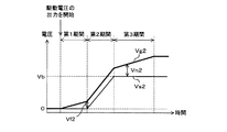
図3は第2半導体スイッチ30のオンへの切替えを説明するためのタイミングチャートである。図3には、第2半導体スイッチ30におけるソースの電圧Vs2及びゲートの電圧Vg2夫々の推移が示されている。以下では、ソースの電圧Vs2及びゲートの電圧Vg2夫々をソース電圧Vs2及びゲート電圧Vg2と記載する。ソース電圧Vs2及びゲート電圧Vg2夫々は、導体12の電位を基準とした電圧である。ゲート電圧Vg2及びソース電圧Vs2夫々の推移は太線及び細線で示されている。ゲート電圧Vg2及びソース電圧Vs2の推移が重なる部分は太線で示されている。
給電制御装置10、及び、比較対象の給電制御装置夫々について、ソース電圧Vs2及びゲート電圧Vg2夫々の推移の傾向は、変わらない。
FIG. 3 is a timing chart for explaining switching of the
The trends in the transition of the source voltage Vs2 and the transition of the gate voltage Vg2 remain unchanged for the power
以下では、駆動部31が駆動電圧の出力を開始してからゲート電圧Vg2がオフ閾値Vf2に到達するまでの期間を第1期間と記載し、ゲート電圧がオフ閾値Vf2に到達してからソース電圧Vs2がバッテリ11の出力電圧Vbに到達するまでの期間を第2期間と記載する。更に、ソース電圧Vs2がバッテリ11の出力電圧Vbに到達してから、ゲート電圧Vg2が駆動電圧に到達するまでの期間を第3期間と記載する。給電制御装置10における第1期間及び第2期間夫々の長さは、比較対象の給電制御装置における第1期間及び第2期間の長さよりも短い。給電制御装置10における第3期間の長さは、比較対象の給電制御装置における第3期間の長さと略同じである。
Hereinafter, a period from when the driving
まず、比較対象の給電制御装置におけるオンへの切替えについて述べる。比較対象の給電制御装置では、第1半導体スイッチ20及び第2半導体スイッチ30がオフである場合、電流が正極端子T1から寄生容量Cs1及び駆動部31の順に流れ、更には、電流が正極端子T1から寄生ダイオードDp1、寄生容量Cd1及び駆動部31の順に流れる。このため、第1半導体スイッチ20において、ゲートの電位を基準としたソース及びドレイン夫々の電圧はバッテリ11の出力電圧Vbと略一致している。従って、第1半導体スイッチ20において、ソース及びドレイン夫々の電位を基準としたゲートの電圧は負である。
First, switching to ON in the power supply control device to be compared will be described. In the power supply control device to be compared, when the
第1期間では、寄生容量Cs1,Cs2が充電される。寄生容量Cs1には、電流が第1半導体スイッチ20のゲートから供給され、寄生容量Cs2には、電流が第2半導体スイッチ30のゲートから供給される。寄生容量Cs2の充電により、ゲート電圧Vg2が上昇する。ゲート電圧Vg2及びソース電圧Vs2の差がオフ閾値Vf2となるまで、ソース電圧Vs2はゼロVに維持される。
In the first period, the parasitic capacitances Cs1 and Cs2 are charged. A current is supplied to the parasitic capacitance Cs1 from the gate of the
ゲート電圧Vg2及びソース電圧Vs2の差がオフ閾値Vf2となった場合、第2半導体スイッチ30のドレイン及びソース間に電流が流れる。このとき、第1半導体スイッチ20はオフであるため、電流は、正極端子T1から、第1半導体スイッチ20の寄生ダイオードDp1を流れる。
When the difference between the gate voltage Vg2 and the source voltage Vs2 becomes the off threshold Vf2, a current flows between the drain and the source of the
負荷A1に電流が流れた場合、負荷A1の両端間に電圧が発生し、ソース電圧Vs2が上昇する。また、負荷A1に流れる電流の上昇と共に、負荷A1の両端間の電圧も上昇する。第2期間では、寄生容量Cs1,Cd1,Cd2が充電される。寄生容量Cd2の充電により、ゲート電圧Vg2が上昇する。寄生容量Cs1,Cd1に関しては、電流が第1半導体スイッチ20のゲートから供給される。寄生容量Cd2に関しては、電流が第2半導体スイッチ30のゲートから供給される。
When a current flows through the load A1, a voltage is generated between both ends of the load A1, and the source voltage Vs2 increases. Further, as the current flowing through the load A1 increases, the voltage between both ends of the load A1 also increases. In the second period, the parasitic capacitances Cs1, Cd1, and Cd2 are charged. The gate voltage Vg2 increases due to the charging of the parasitic capacitance Cd2. With respect to the parasitic capacitances Cs1 and Cd1, current is supplied from the gate of the
ゲート電圧Vg2が上昇した場合、負荷A1に流れる電流が上昇し、ソース電圧Vs2が上昇する。ソース電圧Vs2は、バッテリ11の出力電圧Vbとなるまで、ソース電圧Vs2及びゲート電圧Vg2間の差をオフ閾値Vf2に維持しながら、ゲート電圧Vg2の上昇と共に上昇する。ソース電圧Vs2は、バッテリ11の出力電圧Vbに到達した後、バッテリ11の出力電圧Vbに維持される。 When the gate voltage Vg2 increases, the current flowing through the load A1 increases, and the source voltage Vs2 increases. The source voltage Vs2 increases with the rise of the gate voltage Vg2 while maintaining the difference between the source voltage Vs2 and the gate voltage Vg2 at the off threshold Vf2 until reaching the output voltage Vb of the battery 11. After reaching the output voltage Vb of the battery 11, the source voltage Vs2 is maintained at the output voltage Vb of the battery 11.
第3期間では、寄生容量Cs1,Cd1,Cs2,Cd2が充電される。寄生容量Cs2,Cd2の充電により、ソース電圧Vs2がバッテリ11の出力電圧Vbに維持された状態でゲート電圧Vg2が駆動電圧まで上昇する。ゲート電圧Vg2及びソース電圧Vs2間の差がオン閾値Vn2以上となった時点で、制御回路B1の第2半導体スイッチ30はオンに切替わる。
In the third period, the parasitic capacitances Cs1, Cd1, Cs2, and Cd2 are charged. By charging the parasitic capacitances Cs2 and Cd2, the gate voltage Vg2 increases to the drive voltage while the source voltage Vs2 is maintained at the output voltage Vb of the battery 11. When the difference between the gate voltage Vg2 and the source voltage Vs2 becomes equal to or greater than the ON threshold value Vn2, the
導体12の電位を基準とした第1半導体スイッチ20のゲートの電圧はゲート電圧Vg2と同様に推移し、導体12の電位を基準とした第1半導体スイッチ20のソースの電圧はバッテリ11の出力電圧Vbと略一致している。第1半導体スイッチ20では、ソースの電位を基準としたゲートの電圧は、負の電圧から上昇する。ソースの電位を基準としたゲートの電圧がオン閾値Vn1以上となった場合に第1半導体スイッチ20はオンに切替わる。
The voltage of the gate of the
次に、給電制御装置10におけるオンへの切替えについて述べる。給電制御装置10では、第1半導体スイッチ20及び第2半導体スイッチ30がオフである場合、寄生容量Cs1は抵抗R1を介して放電し、寄生容量Cd1は抵抗R1及び寄生ダイオードDp1を介して放電する。このため、第1半導体スイッチ20において、ソースの電圧を基準としたゲートの電圧と、ドレインの電圧を基準としたゲートの電圧とは略ゼロVである。導体12の電位を基準とした第1半導体スイッチ20のゲートの電圧はバッテリ11の出力電圧Vbと略一致している。
Next, switching to ON in the power
第1期間では、駆動部31が駆動電圧の出力を開始してから、第2半導体スイッチ30のゲート電圧Vg2がバッテリ11の出力電圧Vb以上となるまで、駆動部31から第1半導体スイッチ20のゲートに電圧が出力されることはない。
In the first period, the driving
第1期間では、駆動部31の全ての電力が寄生容量Cs2に供給され、寄生容量Cs2のみが充電される。寄生容量Cs2には、電流が第2半導体スイッチ30のゲートから供給される。寄生容量Cs2の充電により、ゲート電圧Vg2が上昇する。ゲート電圧Vg2及びソース電圧Vs2の差がオフ閾値Vf2となるまで、ソース電圧Vs2はゼロVに維持される。オフ閾値Vf2はバッテリ11の出力電圧Vb未満である。
In the first period, all the power of the
ゲート電圧Vg2及びソース電圧Vs2の差がオフ閾値Vf2となった場合、第2半導体スイッチ30のドレイン及びソース間に電流が流れる。このとき、第1半導体スイッチ20はオフであるため、電流は、正極端子T1から、第1半導体スイッチ20の寄生ダイオードDp1を流れる。
なお、第1期間において、ゲート電圧Vg2の上昇によって、第1半導体スイッチ20のドレインの電圧が上昇する。一方で、第1半導体スイッチ20のゲートの電圧はバッテリ11の出力電圧Vbに維持されている。このため、寄生容量Cd1が充電される。しかしながら、寄生容量Cd1の静電容量は、例えば、寄生容量Cs1の静電容量の10分の1であり、十分に小さいので、第1期間に寄生容量Cd1に供給される電力は無視できる程度に小さい。
When the difference between the gate voltage Vg2 and the source voltage Vs2 becomes the off threshold Vf2, a current flows between the drain and the source of the
In the first period, the voltage of the drain of the
負荷A1に電流が流れた場合、負荷A1の両端間に電圧が発生し、ソース電圧Vs2が上昇する。また、負荷A1に流れる電流の上昇と共に、負荷A1の両端間の電圧も上昇する。第2期間では、寄生容量Cd2が充電され、ゲート電圧Vg2が上昇する。寄生容量Cd2には、電流が第2半導体スイッチ30のゲートから供給される。
When a current flows through the load A1, a voltage is generated between both ends of the load A1, and the source voltage Vs2 increases. Further, as the current flowing through the load A1 increases, the voltage between both ends of the load A1 also increases. In the second period, the parasitic capacitance Cd2 is charged, and the gate voltage Vg2 increases. A current is supplied to the parasitic capacitance Cd2 from the gate of the
給電制御装置10では、比較対象の給電制御装置と同様に、ソース電圧Vs2は、バッテリ11の出力電圧Vbとなるまで、ソース電圧Vs2及びゲート電圧Vg2間の差をオフ閾値Vf2に維持しながら、ゲート電圧Vg2の上昇と共に上昇する。ソース電圧Vs2は、バッテリ11の出力電圧Vbに到達した後、バッテリ11の出力電圧Vbに維持される。
In the power
第3期間では、比較対象の給電制御装置と同様に、寄生容量Cs1,Cd1,Cs2,Cd2が充電される。寄生容量Cs2,Cd2の充電により、ソース電圧Vs2がバッテリ11の出力電圧Vbに維持された状態でゲート電圧Vg2が駆動電圧まで上昇する。ゲート電圧Vg2及びソース電圧Vs2間の差がオン閾値Vn2以上となった時点で、制御回路B1の第2半導体スイッチ30はオンに切替わる。
In the third period, the parasitic capacitances Cs1, Cd1, Cs2, and Cd2 are charged similarly to the power supply control device to be compared. By charging the parasitic capacitances Cs2 and Cd2, the gate voltage Vg2 increases to the drive voltage while the source voltage Vs2 is maintained at the output voltage Vb of the battery 11. When the difference between the gate voltage Vg2 and the source voltage Vs2 becomes equal to or greater than the ON threshold value Vn2, the
導体12の電位を基準とした第1半導体スイッチ20のゲートの電圧は、ゲート電圧Vg2がバッテリ11の出力電圧Vb未満である間、バッテリ11の出力電圧Vbに維持され、ゲート電圧Vg2がバッテリ11の出力電圧Vb以上となった後、ゲート電圧Vg2と同様に推移する。導体12の電位を基準とした第1半導体スイッチ20のソースの電圧はバッテリ11の出力電圧Vbと略一致している。第1半導体スイッチ20では、ソースの電位を基準としたゲートの電圧は、ゼロVから上昇する。ソースの電位を基準としたゲートの電圧がオン閾値Vn1以上となった場合に第1半導体スイッチ20はオンに切替わる。
The gate voltage of the
以上のように、比較対象の給電制御装置では、駆動部31が駆動電圧を出力することによって、第1期間では寄生容量Cs1,Cs2が充電され、第2期間では寄生容量Cs1,Cd1,Cd2が充電され、第3期間では寄生容量Cs1,Cd1,Cs2,Cd2が充電される。駆動部31が駆動電圧を出力した時点の第1半導体スイッチ20では、ソース及びドレイン夫々の電位を基準としたゲートの電圧は負である。このため、第1期間で寄生容量Cs1を充電し、第2期間で寄生容量Cs1,Cd1を充電している。
As described above, in the power supply control device to be compared, when the driving
一方で、給電制御装置10では、駆動部31が駆動電圧を出力することによって、第1期間では寄生容量Cs2が充電され、第2期間では寄生容量Cd2が充電され、第3期間では寄生容量Cs1,Cd1,Cs2,Cd2が充電される。駆動部31が駆動電圧を出力した時点では、第2半導体スイッチ30のゲートの電圧はバッテリ11の出力電圧Vb未満である。第2半導体スイッチ30のゲートの電圧がバッテリ11の出力電圧Vb未満である間、第1半導体スイッチ20のゲートの電圧は、出力電圧Vbに維持され、ソース及びドレイン夫々の電位を基準とした電圧はゼロVである。このため、第1期間では寄生容量Cs1を充電する必要がなく、第2期間では寄生容量Cs1,Cd1を充電する必要がない。
On the other hand, in the power
従って、給電制御装置10では、駆動部31が駆動電圧を出力してから、第1半導体スイッチ20と、第2半導体スイッチ30とがオンに切替わるまでの期間が短い。このため、第1半導体スイッチ20及び第2半導体スイッチ30をオフからオンに切替える場合に生じるスイッチング損失が小さい。更に、電流が第1半導体スイッチ20の寄生ダイオードDp1を流れている期間が短く、消費電力が小さい。
Therefore, in the power
また、給電制御装置10において、駆動部31が、第1半導体スイッチ20及び第2半導体スイッチ30をオンからオフに切替える速度も速い。
In the power
比較対象の給電制御装置では、駆動部31が第2半導体スイッチ30のゲートを、内部抵抗を介して導体12に接続した場合、寄生容量Cs1,Cd1,Cs2,Cd2夫々から電流が駆動部31に流れ、寄生容量Cs1,Cd1,Cs2,Cd2夫々は放電する。前述したように、第1半導体スイッチ20においてソースの電位を基準としたゲートの電圧がオフ閾値Vf1未満となった場合、第1半導体スイッチ20はオフに切替わる。第2半導体スイッチ30においてソースの電位を基準としたゲートの電圧がオフ閾値Vf2未満となった場合、第2半導体スイッチ30はオフに切替わる。
In the power supply control device to be compared, when the driving
給電制御装置10では、駆動部31が、第2半導体スイッチ30のゲートを、内部抵抗を介して導体12に接続した場合、寄生容量Cs2,Cd2夫々から電流が駆動部31に流れ、寄生容量Cs2,Cd2夫々は放電する。寄生容量Cs1,Cd1は抵抗R1を介して放電する。従って、第2半導体スイッチ30において、駆動部31が内部抵抗を介して導体12に接続してから、ソースの電位を基準としたゲートの電圧がオフ閾値Vf2未満となるまでの期間が短い。このため、第1半導体スイッチ20及び第2半導体スイッチ30をオンからオフに切替える場合に生じるスイッチング損失も小さい。
また、給電制御装置10では、駆動部31が第2半導体スイッチ30のゲートの電圧を調整することによって、第1半導体スイッチ20及び第2半導体スイッチ30をオン又はオフに切替えているので、製造費用が安価である。
In the power
Further, in the power
(実施の形態2)
図4は実施の形態2における給電制御装置10の回路図である。
以下では、実施の形態2について、実施の形態1と異なる点を説明する。後述する構成を除く他の構成については、実施の形態1と共通しているため、実施の形態1と共通する構成部には実施の形態1と同一の参照符号を付してその説明を省略する。
(Embodiment 2)
FIG. 4 is a circuit diagram of a power
Hereinafter, points of the second embodiment that are different from the first embodiment will be described. Other configurations except for the configuration described later are common to the first embodiment, and therefore, the same reference numerals as in the first embodiment denote the same components as those in the first embodiment, and a description thereof will be omitted. I do.
実施の形態2における電源システム1において、給電制御装置10、バッテリ11、導体12及び負荷A1は実施の形態1と同様に接続されている。
実施の形態2における給電制御装置10を実施の形態1における給電制御装置10と比較した場合、制御回路B1がキャパシタC1を更に有する点が異なる。キャパシタC1は、第1半導体スイッチ20のゲートと、第2半導体スイッチ30のソースとの間に接続されている。このため、駆動部31が駆動電圧を第2半導体スイッチ30のゲートに出力した場合に、第1半導体スイッチ20は、より速くオフからオンに切替わる。以下では、バッテリ11が正常に接続されている場合における給電制御装置10を説明する。
In the
When the power
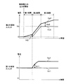
図5は、キャパシタC1の効果を説明するためのタイミングチャートである。図5には、図3と同様に、第2半導体スイッチ30のゲート電圧Vg2及びソース電圧Vs2夫々が太線及び細線によって示されている。実施の形態2における給電制御装置10においても、駆動部31が駆動電圧の出力を開始した場合、ゲート電圧Vg2及びソース電圧Vs2夫々は実施の形態1と同様に推移する。
FIG. 5 is a timing chart for explaining the effect of the capacitor C1. In FIG. 5, similarly to FIG. 3, the gate voltage Vg2 and the source voltage Vs2 of the
図5には、第1半導体スイッチ20におけるソースの電圧Vs1及びゲートの電圧Vg1夫々の推移が更に示されている。以下では、ソースの電圧Vs1及びゲートの電圧Vg1夫々をソース電圧Vs1及びゲート電圧Vg1と記載する。ソース電圧Vs1及びゲート電圧Vg1夫々は、導体12の電位を基準とした電圧である。ゲート電圧Vg1及びソース電圧Vs1夫々の推移は太線及び細線で示されている。ゲート電圧Vg1及びソース電圧Vs1の推移が重なる部分は太線で示されている。
FIG. 5 further shows the transition of the source voltage Vs1 and the gate voltage Vg1 in the
第2半導体スイッチ30がオフである場合、電流が正極端子T1から抵抗R1及びキャパシタC1の順に流れ、キャパシタC1が充電される。キャパシタC1は、キャパシタC1の両端間の電圧がバッテリ11の出力電圧Vbと略一致するまで充電される。駆動部31が駆動電圧を出力する時点では、キャパシタC1の両端間の電圧は、バッテリ11の出力電圧Vbと略一致している。
When the
図5に示すように、ゲート電圧Vg2がバッテリ11の出力電圧Vb未満であり、かつ、ソース電圧Vs2が略ゼロVである場合、ゲート電圧Vg1及びソース電圧Vs1夫々はバッテリ11の出力電圧Vbに維持されている。 As shown in FIG. 5, when the gate voltage Vg2 is lower than the output voltage Vb of the battery 11 and the source voltage Vs2 is substantially zero V, the gate voltage Vg1 and the source voltage Vs1 become the output voltage Vb of the battery 11 respectively. Has been maintained.
実施の形態1で述べたように、第2期間では、ゲート電圧Vg2の上昇と共に、ソース電圧Vs2、即ち、キャパシタC1の負荷A1側の一端における電圧が上昇する。このとき、キャパシタC1の両端間の電圧がバッテリ11の出力電圧Vbに略一致しているため、キャパシタC1における抵抗R1側の一端の電圧がバッテリ11の出力電圧Vbを超え、キャパシタC1から第1半導体スイッチ20の寄生容量Cd1,Cs1に電流が供給され、寄生容量Cd1,Cs1が充電される。結果、ゲート電圧Vg2がバッテリ11の出力電圧Vb未満であるにもかかわらず、ゲート電圧Vg1は、ゲート電圧Vg2の上昇と共に上昇する。
As described in the first embodiment, in the second period, as the gate voltage Vg2 increases, the source voltage Vs2, that is, the voltage at one end of the capacitor C1 on the load A1 side increases. At this time, since the voltage between both ends of the capacitor C1 substantially matches the output voltage Vb of the battery 11, the voltage at one end of the capacitor C1 on the resistor R1 side exceeds the output voltage Vb of the battery 11, and A current is supplied to the parasitic capacitances Cd1 and Cs1 of the
第1半導体スイッチ20のソース電圧Vs1は、バッテリ11の出力電圧Vbに維持されている。ゲート電圧Vg1及びソース電圧Vs1の差がオン閾値Vn1以上となった場合、第1半導体スイッチ20はオンに切替わる。その後、ゲート電圧Vg1は、駆動部31が出力している駆動電圧に維持され、安定する。
以上のように、実施の形態2における給電制御装置10においては、駆動部31が駆動電圧を出力してから第1半導体スイッチ20がオンに切替わるまでの期間が更に短い。このように、第1半導体スイッチ20は、より速くオンに切替わるため、第1半導体スイッチ20において、電流が寄生ダイオードDp1を流れている期間が更に短く、第1半導体スイッチ20で消費される電力が更に小さい。
The source voltage Vs1 of the
As described above, in the power
第1半導体スイッチ20及び第2半導体スイッチ30がオンである場合、第2半導体スイッチ30のソース電圧Vs2はバッテリ11の出力電圧Vbに略一致しており、第1半導体スイッチ20のゲート電圧Vg1は、駆動部31が出力した駆動電圧に略一致している。
When the
更に、第1半導体スイッチ20のゲートと、第2半導体スイッチ30のソースとの間にキャパシタC1が接続されているので、駆動部31が、第2半導体スイッチ30のゲートを、内部抵抗を介して導体12に接続した場合に、第1半導体スイッチ20は、より速くオンからオフに切替わる。
Furthermore, since the capacitor C1 is connected between the gate of the
駆動部31が、第2半導体スイッチ30のゲートを、内部抵抗を介して導体12に接続した場合、実施の形態1で述べたように、寄生容量Cd2,Cs2は放電し、第2半導体スイッチ30のゲート電圧Vg2は低下する。これにより、第2半導体スイッチ30のドレイン及びソース間の抵抗値が上昇し、負荷A1に流れる電流が低下し、第2半導体スイッチ30のソース電圧Vg2が低下する。ソース電圧Vs2の低下と共に、キャパシタC1における抵抗R1側の一端の電圧も低下する。
When the
駆動部31が、第2半導体スイッチ30のゲートを、内部抵抗を介して導体12に接続した場合、寄生容量Cd1,Cs1は、実施の形態1と同様に抵抗R1を介して放電する。更に、実施の形態2における給電制御装置10では、キャパシタC1における抵抗R1側の一端の電圧が低下するため、寄生容量Cd1,Cs1からキャパシタC1にも電流が流れる。これにより、寄生容量Cd1,Cs1は放電し、キャパシタC1は充電される。
When the
従って、寄生容量Cd1,Cs1は、抵抗R1を介して放電すると共に、キャパシタC1に放電するため、第1半導体スイッチ20のゲートの電圧が、より速く低下し、第1半導体スイッチ20は、より速くオンからオフに切替わる。
Accordingly, the parasitic capacitances Cd1 and Cs1 are discharged through the resistor R1 and discharged to the capacitor C1, so that the voltage of the gate of the
実施の形態2における給電制御装置10は、実施の形態1における給電制御装置10が有する全ての構成部を有しているので、実施の形態1における給電制御装置10が奏する効果を同様に奏する。
The power
(実施の形態3)
実施の形態2においては、給電制御装置10が給電を制御する負荷の数は1つである。しかしながら、給電制御装置10が給電を制御する負荷の数は2以上であってもよい。
以下では、実施の形態3について、実施の形態2と異なる点を説明する。後述する構成を除く他の構成については、実施の形態2と共通しているため、実施の形態2と共通する構成部には実施の形態2と同一の参照符号を付してその説明を省略する。
(Embodiment 3)
In the second embodiment, the number of loads for which power
Hereinafter, points of the third embodiment that are different from the second embodiment will be described. Since other configurations except for the configuration described later are common to the second embodiment, the same reference numerals as in the second embodiment denote the same components as those in the second embodiment, and a description thereof will be omitted. I do.
図6は、実施の形態3における電源システム1の要部構成を示すブロック図である。実施の形態3における電源システム1は、実施の形態2と同様に、給電制御装置10、バッテリ11、導体12及び負荷A1を有する。これらは、実施の形態2と同様に接続されている。実施の形態3における電源システム1は、更に、(n−1)(n:2以上の整数)個の負荷A2,A3,・・・,Anを備える。負荷A2,A3,・・・,An夫々の一端は給電制御装置10に接続され、負荷A2,A3,・・・,An夫々の他端は導体12に接続されている。
FIG. 6 is a block diagram showing a main configuration of
バッテリ11が正常に接続されている場合、給電制御装置10を介して、バッテリ11からn個の負荷A1,A2,・・・,Anに給電される。給電制御装置10は、バッテリ11からn個の負荷A1,A2,・・・,Anへの給電を各別に制御する。負荷A2,A3,・・・,An夫々は、負荷A1と同様に、車両に搭載された電気機器であり、給電されている場合に作動し、給電が停止している場合に動作を停止している。
バッテリ11の接続を誤った場合、給電制御装置10は、負極端子T2からn個の負荷A1,A2,・・・,Anに電流が流れることを防止する。
When the battery 11 is normally connected, power is supplied from the battery 11 to the n loads A1, A2, ..., An via the power
When the connection of the battery 11 is incorrect, the power
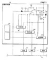
図7は給電制御装置10の回路図である。実施の形態3における給電制御装置10は、実施の形態2における給電制御装置10と同様に、第1半導体スイッチ20、スイッチ21、マイコン22、制御回路B1、寄生容量Cd1,Cs1、寄生ダイオードDp1、ダイオードD1及び抵抗R1,R2,R3を有する。これらは、実施の形態2と同様に接続されている。
FIG. 7 is a circuit diagram of the power
実施の形態3における給電制御装置10は、更に、(n−1)個の制御回路B2,B3,・・・,Bnを有する。制御回路B2,B3,・・・,Bn夫々は、第1半導体スイッチ20のゲート及びドレインと、マイコン22とに各別に接続されている。制御回路B2,B3,・・・,Bn夫々は、更に、負荷A2,A3,・・・,Anの一端に接続されている。
The power
図8は制御回路Bk(k=1,2,・・・,n)の回路図である。実施の形態3における制御回路Bkは、実施の形態2における制御回路B1と同様に、第2半導体スイッチ30、駆動部31、寄生容量Cs2,Cd2、キャパシタC1、寄生ダイオードDp2及びダイオードD2を有する。
FIG. 8 is a circuit diagram of the control circuit Bk (k = 1, 2,..., N). The control circuit Bk according to the third embodiment includes the
第2半導体スイッチ30、駆動部31、寄生容量Cs2,Cd2、寄生ダイオードDp2及びダイオードD2は、第2半導体スイッチ30のソースの接続先を除いて、実施の形態2と同様に接続されている。
従って、制御回路Bkの第2半導体スイッチ30のドレインは、第1半導体スイッチ20のドレインに接続されている。更に、制御回路BkのダイオードD2のカソードは第1半導体スイッチ20のゲートに接続され、制御回路BkのダイオードD2のアノードは、制御回路Bkの第2半導体スイッチ30のゲートに接続されている。
The
Therefore, the drain of the
制御回路Bkが有する第2半導体スイッチ30のソースは負荷Akの一端に接続されている。
制御回路Bkは、更に、ダイオードD3,D4を有する。制御回路Bkにおいて、ダイオードD3のカソードは第1半導体スイッチ20のゲートに接続されている。ダイオードD3のアノードは、ダイオードD4のカソードと、キャパシタC1の一端とに接続されている。ダイオードD4のアノードは、第1半導体スイッチ20のドレインに接続されている。キャパシタC1の他端は第2半導体スイッチ30のソースに接続されている。寄生ダイオードDp1,Dp2及びダイオードD2夫々の順方向の電圧降下の幅と同様に、ダイオードD3,D4夫々の順方向の電圧降下の幅も十分に小さいとみなす。
The source of the
The control circuit Bk further includes diodes D3 and D4. In the control circuit Bk, the cathode of the diode D3 is connected to the gate of the
実施の形態3において、給電制御装置10は、前述したように、n個の制御回路B1,B2,・・・,Bnを有し、制御回路Bk(k=1,2,・・・,n)は、第2半導体スイッチ30、キャパシタC1及びダイオードD2,D3,D4を有する。このため、給電制御装置10が有する第2半導体スイッチ30、キャパシタC1及びダイオードD2,D3,D4夫々の数は、nであり、同じである。
ダイオードD3は第2のダイオードとして機能し、ダイオードD4は第3のダイオードとして機能する。
In the third embodiment, as described above, the power
The diode D3 functions as a second diode, and the diode D4 functions as a third diode.
制御回路Bk(k=1,2,・・・,n)の駆動部31には、マイコン22から、負荷Akの駆動を指示する駆動信号と、負荷Akの駆動の停止を指示する停止信号とが入力される。
制御回路Bkの駆動部31は、実施の形態2における駆動部31と同様に、駆動信号が入力された場合、図示しない内部抵抗を介して、駆動電圧を制御回路Bkの第2半導体スイッチ30のゲートと、第1半導体スイッチ20のゲートとに出力する。これにより、第1半導体スイッチ20、及び、制御回路Bkの第2半導体スイッチ30夫々のゲートの電圧が上昇し、第1半導体スイッチ20と、制御回路Bkの第2半導体スイッチ30とがオンに切替わる。
The
Similarly to the
制御回路Bkの第2半導体スイッチ30がオンである場合、電流は、正極端子T1から、第1半導体スイッチ20のソース及びドレイン、並びに、制御回路Bkの第2半導体スイッチ30のドレイン及びソースの順に流れる。第1半導体スイッチ20と、制御回路Bkの第2半導体スイッチ30とがオンである場合、負荷Akに給電され、負荷Akが作動する。
When the
制御回路Bkの駆動部31は、停止信号が入力された場合、実施の形態2における駆動部31と同様に、制御回路Bkの第2半導体スイッチ30のゲートを、内部抵抗を介して導体12に接続させる。これにより、制御回路Bkの寄生容量Cs2,Cd2が放電し、制御回路Bkの第2半導体スイッチ30のゲートの電圧は、オフ閾値Vf2未満となり、第2半導体スイッチ30はオフに切替わる。これにより、負荷Akへの給電が停止し、負荷Akは動作を停止する。
マイコン22は、n個の制御回路B1,B2,・・・,Bn夫々の駆動部31に駆動信号又は停止信号を出力することによって、n個の制御回路B1,B2,・・・,Bnの動作を各別に制御する。
When the stop signal is input, the
The
マイコン22がn個の制御回路B1,B2,・・・,Bn夫々の駆動部31に停止信号を出力し、n個の制御回路B1,B2,・・・,Bn夫々の駆動部31が第2半導体スイッチ30のゲートを導体12に接続させた場合、第1半導体スイッチ20のゲートへの電圧の出力が停止する。この場合、寄生容量Cs1,Cd1夫々は抵抗R1を介して放電する。これにより、第1半導体スイッチ20において、ソースの電位を基準としたゲートの電圧はオフ閾値Vf1未満となり、第1半導体スイッチ20はオフに切替わる。
The
以上のように、n個の制御回路B1,B2,・・・,Bnの駆動部31は、n個の第2半導体スイッチ30のゲートの電圧を各別に調整し、n個の第2半導体スイッチ30を各別にオン又はオフに切替える。これにより、n個の第2半導体スイッチ30夫々を介した負荷A1,A2,・・・,Anへの給電を制御する。実施の形態3では、n個の駆動部31が切替え部として機能する。
As described above, the
n個の駆動部31中の少なくとも1つが駆動電圧を出力した場合、即ち、n個の第2半導体スイッチ30中の少なくとも1つをオンに切替える場合、第1半導体スイッチ20がオンに切替わる。また、n個の駆動部31の全てが第2半導体スイッチ30のゲートを、内部抵抗を介して導体12に接続させた場合、即ち、n個の第2半導体スイッチ30の全てをオフに切替える場合、第1半導体スイッチ20がオフに切替わる。
When at least one of the
更に、複数の第2半導体スイッチ30がオンである場合において、オンである複数の第2半導体スイッチ30中の1つのゲートが駆動部31の内部抵抗を介して導体12に接続されたとき、ダイオードD2の作用により、寄生容量Cs1,Cd1が放電することはない。このため、1つの駆動部31が第2半導体スイッチ30のゲートを、内部抵抗を介して導体12に接続させた場合であっても、他の駆動部31中の少なくとも1つが駆動電圧を出力している限り、内部抵抗を介して導体12に接続された第2半導体スイッチ30のみがオフに切替わる。
Further, in the case where the plurality of second semiconductor switches 30 are on, when one of the gates of the plurality of second semiconductor switches 30 that are on is connected to the
第1半導体スイッチ20と、n個の第2半導体スイッチ30とがオフである状態で、制御回路Bkの駆動部31が駆動電圧を出力した場合、実施の形態2と同様に、キャパシタC1の作用により、第1半導体スイッチ20がより速くオンに切替わる。
When the driving
制御回路Bkの第2半導体スイッチ30がオフである場合において、第1半導体スイッチ20がオフであるとき、正極端子T1から、電流が寄生ダイオードDp1及びダイオードD4を介してキャパシタC1に流れ、キャパシタC1が充電される。同様の場合において、第1半導体スイッチ20がオンであるとき、正極端子T1から、電流が第1半導体スイッチ20及びダイオードD4を介してキャパシタC1に流れ、キャパシタC1が充電される。制御回路Bkの第2半導体スイッチ30がオフである場合、第1半導体スイッチ20がオンであるか否かに無関係に、キャパシタC1は、キャパシタC1の両端間の電圧がバッテリ11の出力電圧Vbに略一致するまで充電される。
When the
第1半導体スイッチ20と、n個の第2半導体スイッチ30とがオフである状態で、制御回路Bkの駆動部31が駆動電圧を出力した場合における給電制御装置10の動作を説明する。第2半導体スイッチ30のゲートの電圧がバッテリ11の出力電圧Vb未満であり、かつ、第2半導体スイッチ30のソースの電圧が略ゼロVである場合、実施の形態2と同様に、第1半導体スイッチ20のゲート及びソース夫々の電圧はバッテリ11の出力電圧Vbに維持されている。
The operation of the power
第2半導体スイッチ30のゲートの電圧の上昇と共に、第2半導体スイッチ30のソースの電圧が上昇する第2期間では、実施の形態2と同様に、キャパシタC1の両端間の電圧がバッテリ11の出力電圧Vbに略一致しているため、キャパシタC1における抵抗R1側の一端の電圧がバッテリ11の出力電圧Vbを超える。これにより、キャパシタC1からダイオードD3を介して第1半導体スイッチ20の寄生容量Cd1,Cs1に電流が供給され、寄生容量Cd1,Cs1が充電される。結果、ゲート電圧Vg2がバッテリ11の出力電圧Vb未満であるにもかかわらず、ゲート電圧Vg1は、ゲート電圧Vg2の上昇と共に上昇する。
In the second period in which the voltage of the source of the
第1半導体スイッチ20のソースの電圧は、バッテリ11の出力電圧Vbに維持されている。第1半導体スイッチ20のゲート電圧Vg1及びソース電圧Vs1の差がオン閾値Vn1以上となった場合、第1半導体スイッチ20はオンに切替わる。その後、ゲート電圧Vg1は、バッテリ11の出力電圧Vbに維持され、安定する。
The voltage of the source of the
以上のように、実施の形態3における給電制御装置10においては、駆動部31が駆動電圧を出力してから第1半導体スイッチ20がオンに切替わるまでの期間が更に短い。このように、第1半導体スイッチ20は、より速くオンに切替わるため、第1半導体スイッチ20において、電流が寄生ダイオードDp1を流れている期間が短く、第1半導体スイッチ20で消費される電力が小さい。
As described above, in the power
実施の形態3においては、ダイオードD3は、ダイオードD2と同様に、オンである複数の第2半導体スイッチ30中の1つがオフに切替わったと同時に第1半導体スイッチ20がオフに切替わることを防止する。制御回路Bkにおいて、駆動部31が駆動電圧の出力を停止して第2半導体スイッチ30のゲートを、内部抵抗を介して導体12に接続させた場合、実施の形態2と同様に、寄生容量Cs2,Cd2が放電し、第2半導体スイッチ30のゲートの電圧が低下する。これにより、負荷Akを流れる電流が低下するため、第2半導体スイッチ30のソースの電圧、即ち、負荷Akの両端間の電圧が低下する。
In the third embodiment, like the diode D2, the diode D3 prevents the
第2半導体スイッチ30のソースの電圧が低下した場合、キャパシタC1の抵抗R1側の一端の電圧が低下する。しかしながら、制御回路BkではダイオードD3が設けられているため、寄生容量Cs1,Cd1からキャパシタC1に電流が流れることはない。従って、n個の駆動部31中の1つが、駆動電圧の出力を停止して第2半導体スイッチ30のゲートを、内部抵抗を介して導体12に接続した場合であっても、他の駆動部31中の少なくとも1つが駆動電圧を出力している限り、第1半導体スイッチ20はオンに維持される。従って、n個の負荷A1,A2,・・・,Anの中で複数の負荷が作動している場合において、作動中の負荷の1つの動作を停止させたときに、作動中の他の負荷が不意に動作を停止することはない。
When the voltage at the source of the
実施の形態3において、給電制御装置10は抵抗R1を有し、制御回路Bk(k=1,2,・・・,n)はダイオードD2を有するので、実施の形態1,2と同様に、第1半導体スイッチ20及び第2半導体スイッチ30は短い期間でオン又はオフに切替わり、スイッチング損失が小さい。また、n個の駆動部31は、n個の第2半導体スイッチ30夫々のゲートの電圧を調整することによって、第1半導体スイッチとn個の第2半導体スイッチ30とをオン又はオフに切替えるので給電制御装置10の製造費用は安価である。更に、バッテリ11の接続を誤った場合に第1半導体スイッチ20がオフに切替わるので、負極端子T2からn個の負荷A1,A2,・・・,Anに電流が流れることが確実に防止される。
In the third embodiment, the power
なお、実施の形態1〜3において、スイッチ21は、バッテリ11の接続を誤った場合にオフからオンに切替わるスイッチであればよいため、NPN型のバイポーラトランジスタに限定されず、PNP型のバイポーラトランジスタ又はFET等であってもよい。
In the first to third embodiments, since the
開示された実施の形態1〜3は、全ての点で例示であって制限的なものではないと考えられるべきである。本発明の範囲は上述の説明ではなくて特許請求の範囲によって示され、特許請求の範囲と均等の意味及び範囲内での全ての変更が含まれることが意図される。 The disclosed Embodiments 1 to 3 are to be considered in all respects as illustrative and not restrictive. The scope of the present invention is defined by the terms of the claims, rather than the description above, and is intended to include any modifications within the scope and meaning equivalent to the terms of the claims.
10 給電制御装置
20 第1半導体スイッチ
21 スイッチ
30 第2半導体スイッチ
31 駆動部(切替え部の一部)
C1 キャパシタ
Dp1 寄生ダイオード
D2 ダイオード
D3 ダイオード(第2のダイオード)
D4 ダイオード(第3のダイオード)
R1 抵抗
C1 capacitor Dp1 parasitic diode D2 diode D3 diode (second diode)
D4 diode (third diode)
R1 resistance
Claims (6)
前記第1半導体スイッチ及び第2半導体スイッチ夫々は、制御端の電圧がオン閾値以上である場合にオンに切替わり、該制御端の電圧がオフ閾値未満である場合にオフに切替わり、
前記第1半導体スイッチの前記電流入力端及び制御端間に接続される抵抗と、
カソードが前記第1半導体スイッチの前記制御端に接続され、アノードが前記第2半導体スイッチの前記制御端に接続されるダイオードと
を備え、
前記切替え部は、前記第2半導体スイッチの前記制御端の電圧を調整することによって前記切替えを行い、
前記切替え部がオン又はオフに切替える半導体スイッチは、前記第1半導体スイッチ及び第2半導体スイッチのみであること
を特徴とする給電制御装置。 A switching unit for switching on and off a first semiconductor switch and a second semiconductor switch having a current input terminal connected to a current output terminal of the first semiconductor switch, wherein the switching unit switches the second semiconductor switch. In a power supply control device that controls power supply via a semiconductor switch,
Each of the first semiconductor switch and the second semiconductor switch is turned on when the voltage of the control terminal is equal to or higher than the on threshold, and is turned off when the voltage of the control terminal is lower than the off threshold.
A resistor connected between the current input terminal and the control terminal of the first semiconductor switch;
A diode having a cathode connected to the control terminal of the first semiconductor switch and an anode connected to the control terminal of the second semiconductor switch;
The switching unit may have the line switching said by adjusting the voltage of the control terminal of the second semiconductor switches,
The power supply control device according to claim 1, wherein the semiconductor switches that the switching unit switches on or off are only the first semiconductor switches and the second semiconductor switches .
前記第1半導体スイッチ及び第2半導体スイッチ夫々は、制御端の電圧がオン閾値以上である場合にオンに切替わり、該制御端の電圧がオフ閾値未満である場合にオフに切替わり、
前記第1半導体スイッチの前記電流入力端及び制御端間に接続される抵抗と、
カソードが前記第1半導体スイッチの前記制御端に接続され、アノードが前記第2半導体スイッチの前記制御端に接続されるダイオードと、
カソード及びアノードが前記第1半導体スイッチの前記電流出力端及び電流入力端に接続される寄生ダイオードと、
前記第1半導体スイッチの前記制御端、及び、前記第2半導体スイッチの前記電流出力端の間に接続されるキャパシタと
を備え、
前記切替え部は、前記第2半導体スイッチの前記制御端の電圧を調整することによって前記切替えを行うこと
を特徴とする給電制御装置。 A switching unit for switching on and off a first semiconductor switch and a second semiconductor switch having a current input terminal connected to a current output terminal of the first semiconductor switch, wherein the switching unit switches the second semiconductor switch. In a power supply control device that controls power supply via a semiconductor switch,
Each of the first semiconductor switch and the second semiconductor switch is turned on when the voltage of the control terminal is equal to or higher than the on threshold, and is turned off when the voltage of the control terminal is lower than the off threshold.
A resistor connected between the current input terminal and the control terminal of the first semiconductor switch;
A diode having a cathode connected to the control terminal of the first semiconductor switch and an anode connected to the control terminal of the second semiconductor switch;
A parasitic diode having a cathode and an anode connected to the current output terminal and the current input terminal of the first semiconductor switch;
A capacitor connected between the control terminal of the first semiconductor switch and the current output terminal of the second semiconductor switch ;
The switching unit includes a paper electrostatic controller you and performs switching said by adjusting the voltage of the control terminal of the second semiconductor switch.
前記第1半導体スイッチ及び第2半導体スイッチ夫々は、制御端の電圧がオン閾値以上である場合にオンに切替わり、該制御端の電圧がオフ閾値未満である場合にオフに切替わり、
前記第1半導体スイッチの前記電流入力端及び制御端間に接続される抵抗と、
カソードが前記第1半導体スイッチの前記制御端に接続され、アノードが前記第2半導体スイッチの前記制御端に接続されるダイオードと
を備え、
前記第2半導体スイッチ及びダイオード夫々の数は、2以上であって同じであり、
複数の前記第2半導体スイッチ夫々の前記電流入力端は、前記第1半導体スイッチの電流出力端に接続され、
複数の前記ダイオードのカソードは第1半導体スイッチの前記制御端に接続され、
前記複数のダイオード夫々のアノードは、前記複数の第2半導体スイッチの制御端に接続され、
前記切替え部は、前記複数の第2半導体スイッチの前記制御端の電圧を各別に調整すること
を特徴とする給電制御装置。 A switching unit for switching on and off a first semiconductor switch and a second semiconductor switch having a current input terminal connected to a current output terminal of the first semiconductor switch, wherein the switching unit switches the second semiconductor switch. In a power supply control device that controls power supply via a semiconductor switch,
Each of the first semiconductor switch and the second semiconductor switch is turned on when the voltage of the control terminal is equal to or higher than the on threshold, and is turned off when the voltage of the control terminal is lower than the off threshold.
A resistor connected between the current input terminal and the control terminal of the first semiconductor switch;
A diode having a cathode connected to the control terminal of the first semiconductor switch and an anode connected to the control terminal of the second semiconductor switch;
With
The number of each of the second semiconductor switch and the diode is equal to or greater than two, and
The current input terminal of each of the plurality of second semiconductor switches is connected to a current output terminal of the first semiconductor switch,
The cathodes of the plurality of diodes are connected to the control terminal of a first semiconductor switch,
An anode of each of the plurality of diodes is connected to a control terminal of the plurality of second semiconductor switches,
The switching unit includes a paper electrostatic controller you and adjusts the voltage of the control terminal of said plurality of second semiconductor switches each another.
カソードが前記第1半導体スイッチの前記制御端に接続される複数の第2のダイオードと、
カソードが前記複数の第2のダイオード夫々のアノードに接続され、アノードが前記第1半導体スイッチの前記電流出力端に接続される複数の第3のダイオードと、
一端が前記複数の第2のダイオード夫々のアノードに接続される複数のキャパシタと
を備え、
前記第2のダイオード、第3のダイオード及びキャパシタ夫々の数は前記第2半導体スイッチの数と同じであり、
前記複数のキャパシタ夫々の他端は、前記複数の第2半導体スイッチの前記電流出力端に接続されること
を特徴とする請求項3に記載に給電制御装置。 A parasitic diode having a cathode and an anode connected to the current output terminal and the current input terminal of the first semiconductor switch;
A plurality of second diodes having a cathode connected to the control end of the first semiconductor switch;
A plurality of third diodes having a cathode connected to an anode of each of the plurality of second diodes, and an anode connected to the current output terminal of the first semiconductor switch;
A plurality of capacitors each having one end connected to an anode of each of the plurality of second diodes;
The number of each of the second diode, the third diode, and the capacitor is the same as the number of the second semiconductor switches;
The power supply control device according to claim 3, wherein the other end of each of the plurality of capacitors is connected to the current output terminals of the plurality of second semiconductor switches.
前記第1半導体スイッチ及び第2半導体スイッチ夫々は、制御端の電圧がオン閾値以上である場合にオンに切替わり、該制御端の電圧がオフ閾値未満である場合にオフに切替わり、
前記第1半導体スイッチの前記電流入力端及び制御端間に接続される抵抗と、
カソードが前記第1半導体スイッチの前記制御端に接続され、アノードが前記第2半導体スイッチの前記制御端に接続されるダイオードと
を備え、
前記切替え部は、前記第2半導体スイッチの前記制御端の電圧を調整することによって前記切替えを行い、
前記第1半導体スイッチは、電流入力端の電位を基準とした前記制御端の電圧に基づいてオン又はオフに切替わり、
前記第2半導体スイッチは、電流出力端の電位を基準とした前記制御端の電圧に基づいてオン又はオフに切替わること
を特徴とする給電制御装置。 A switching unit for switching on and off a first semiconductor switch and a second semiconductor switch having a current input terminal connected to a current output terminal of the first semiconductor switch, wherein the switching unit switches the second semiconductor switch. In a power supply control device that controls power supply via a semiconductor switch,
Each of the first semiconductor switch and the second semiconductor switch is turned on when the voltage of the control terminal is equal to or higher than the on threshold, and is turned off when the voltage of the control terminal is lower than the off threshold.
A resistor connected between the current input terminal and the control terminal of the first semiconductor switch;
A diode having a cathode connected to the control terminal of the first semiconductor switch and an anode connected to the control terminal of the second semiconductor switch;
With
The switching unit performs the switching by adjusting a voltage of the control terminal of the second semiconductor switch,
The first semiconductor switch is turned on or off based on a voltage at the control terminal with reference to a potential at a current input terminal;
It said second semiconductor switch, supplying electric controller you characterized in that switched on or off based on the voltage of the control terminal relative to the potential of the current output.
前記第1半導体スイッチは、電流入力端及び制御端間の電圧が略ゼロVである場合にオフであること
を特徴とする請求項5に記載の給電制御装置。 When a negative voltage is applied to the current input terminal of the first semiconductor switch, which is connected between the current input terminal and the control terminal of the first semiconductor switch and based on the potential of the current output terminal of the second semiconductor switch. Equipped with a switch that switches on,
The power supply control device according to claim 5, wherein the first semiconductor switch is off when a voltage between a current input terminal and a control terminal is substantially zero volt.
Priority Applications (5)
| Application Number | Priority Date | Filing Date | Title |
|---|---|---|---|
| JP2016075885A JP6668897B2 (en) | 2016-04-05 | 2016-04-05 | Power supply control device |
| PCT/JP2017/011413 WO2017175584A1 (en) | 2016-04-05 | 2017-03-22 | Power supply control device |
| CN201780017479.1A CN108781078B (en) | 2016-04-05 | 2017-03-22 | Power supply control device |
| US16/090,427 US10411696B2 (en) | 2016-04-05 | 2017-03-22 | Power supply control device |
| DE112017001921.4T DE112017001921T5 (en) | 2016-04-05 | 2017-03-22 | Power supply control means |
Applications Claiming Priority (1)
| Application Number | Priority Date | Filing Date | Title |
|---|---|---|---|
| JP2016075885A JP6668897B2 (en) | 2016-04-05 | 2016-04-05 | Power supply control device |
Publications (3)
| Publication Number | Publication Date |
|---|---|
| JP2017188773A JP2017188773A (en) | 2017-10-12 |
| JP2017188773A5 JP2017188773A5 (en) | 2018-08-30 |
| JP6668897B2 true JP6668897B2 (en) | 2020-03-18 |
Family
ID=60001139
Family Applications (1)
| Application Number | Title | Priority Date | Filing Date |
|---|---|---|---|
| JP2016075885A Active JP6668897B2 (en) | 2016-04-05 | 2016-04-05 | Power supply control device |
Country Status (5)
| Country | Link |
|---|---|
| US (1) | US10411696B2 (en) |
| JP (1) | JP6668897B2 (en) |
| CN (1) | CN108781078B (en) |
| DE (1) | DE112017001921T5 (en) |
| WO (1) | WO2017175584A1 (en) |
Families Citing this family (9)
| Publication number | Priority date | Publication date | Assignee | Title |
|---|---|---|---|---|
| JP6668897B2 (en) * | 2016-04-05 | 2020-03-18 | 株式会社オートネットワーク技術研究所 | Power supply control device |
| JP6740709B2 (en) * | 2016-05-20 | 2020-08-19 | 株式会社オートネットワーク技術研究所 | Power supply control device |
| JP6891835B2 (en) * | 2018-02-22 | 2021-06-18 | 株式会社オートネットワーク技術研究所 | Control device |
| JP7026016B2 (en) * | 2018-07-20 | 2022-02-25 | ルネサスエレクトロニクス株式会社 | Semiconductor devices and electronic control devices |
| JP2022080104A (en) * | 2020-11-17 | 2022-05-27 | 株式会社オートネットワーク技術研究所 | Power supply control device, power supply control method, and computer program |
| CN112994436B (en) * | 2021-02-04 | 2022-06-03 | 重庆先进光电显示技术研究院 | Grid opening voltage generation circuit, display panel driving device and display device |
| JP2022149753A (en) * | 2021-03-25 | 2022-10-07 | 株式会社オートネットワーク技術研究所 | Latch circuit and power feeding control device |
| CN113708467B (en) * | 2021-10-29 | 2022-02-22 | 苏州浪潮智能科技有限公司 | Electrifying circuit, battery backup unit and storage server system |
| US20230216402A1 (en) * | 2022-01-04 | 2023-07-06 | Nuvolta Technologies (Hefei) Co., Ltd. | Gate Drive Voltage Regulation Apparatus and Control Method |
Family Cites Families (21)
| Publication number | Priority date | Publication date | Assignee | Title |
|---|---|---|---|---|
| JPH0998567A (en) * | 1995-07-27 | 1997-04-08 | Toshiyasu Suzuki | Insulating power supply means and voltage transforming means |
| DE19848159A1 (en) * | 1998-10-20 | 2000-04-27 | Bosch Gmbh Robert | Polarity inversion protection circuit for electronic final power stage has n-channel power FET that receives fed back drive voltage(s) from electronics to high side semiconducting switch(es) |
| JP4149778B2 (en) * | 2002-10-28 | 2008-09-17 | 矢崎総業株式会社 | Vehicle power control device |
| JP4150297B2 (en) * | 2003-06-30 | 2008-09-17 | ソニー株式会社 | Field effect transistor drive circuit |
| JP2006108568A (en) * | 2004-10-08 | 2006-04-20 | Sanyo Electric Co Ltd | Switching element and protection circuit using the same |
| JP2006158185A (en) * | 2004-10-25 | 2006-06-15 | Toshiba Corp | Power semiconductor device |
| CN1909325A (en) * | 2005-08-01 | 2007-02-07 | 三洋电机株式会社 | Battery pack with circuit protection function |
| JP2008109349A (en) * | 2006-10-25 | 2008-05-08 | Matsushita Electric Ind Co Ltd | Reverse current prevention circuit |
| US20100103576A1 (en) * | 2007-03-05 | 2010-04-29 | Hitoshi Sugimoto | Glow plug driver |
| JP4536108B2 (en) * | 2007-12-12 | 2010-09-01 | Okiセミコンダクタ株式会社 | Load drive circuit |
| JP5217849B2 (en) * | 2008-09-29 | 2013-06-19 | サンケン電気株式会社 | Electrical circuit switching device |
| JP2014003514A (en) * | 2012-06-20 | 2014-01-09 | Renesas Electronics Corp | Semiconductor device and communication system |
| JP5772776B2 (en) * | 2012-09-28 | 2015-09-02 | 株式会社オートネットワーク技術研究所 | Power supply control device |
| JP5502216B1 (en) * | 2013-02-28 | 2014-05-28 | 三菱電機株式会社 | Branch power supply control device and branch power control method for electric load |
| JP6157752B2 (en) * | 2014-09-09 | 2017-07-05 | 三菱電機株式会社 | Inverter device for driving multiphase AC motor |
| WO2017009990A1 (en) * | 2015-07-15 | 2017-01-19 | 株式会社 東芝 | Semiconductor device |
| JP6566355B2 (en) * | 2015-09-11 | 2019-08-28 | パナソニックIpマネジメント株式会社 | Power converter |
| US10069439B2 (en) * | 2015-12-22 | 2018-09-04 | Renesas Electronics Corporation | Power conversion system, power module, and semiconductor device with diode coupling |
| DE112017000686T5 (en) * | 2016-03-04 | 2018-10-18 | Nidec Corporation | POWER CONVERSION DEVICE, ENGINE DRIVE UNIT AND ELECTRIC POWER STEERING DEVICE |
| JP6668897B2 (en) * | 2016-04-05 | 2020-03-18 | 株式会社オートネットワーク技術研究所 | Power supply control device |
| CN108695843B (en) * | 2017-03-29 | 2023-09-22 | 太阳能安吉科技有限公司 | Bypass circuit and method of bypassing power module in power system |
-
2016
- 2016-04-05 JP JP2016075885A patent/JP6668897B2/en active Active
-
2017
- 2017-03-22 CN CN201780017479.1A patent/CN108781078B/en active Active
- 2017-03-22 DE DE112017001921.4T patent/DE112017001921T5/en active Pending
- 2017-03-22 WO PCT/JP2017/011413 patent/WO2017175584A1/en active Application Filing
- 2017-03-22 US US16/090,427 patent/US10411696B2/en active Active
Also Published As
| Publication number | Publication date |
|---|---|
| DE112017001921T5 (en) | 2018-12-13 |
| US10411696B2 (en) | 2019-09-10 |
| JP2017188773A (en) | 2017-10-12 |
| US20190123739A1 (en) | 2019-04-25 |
| WO2017175584A1 (en) | 2017-10-12 |
| CN108781078A (en) | 2018-11-09 |
| CN108781078B (en) | 2021-11-16 |
Similar Documents
| Publication | Publication Date | Title |
|---|---|---|
| JP6668897B2 (en) | Power supply control device | |
| WO2017175578A1 (en) | Power supply control device | |
| CN108701990B (en) | Power supply control device | |
| WO2017122664A1 (en) | Power feed control device | |
| US10396661B2 (en) | Power supply control apparatus | |
| JP6708003B2 (en) | Power supply control device | |
| CN110190840B (en) | Control device | |
| WO2023231318A1 (en) | Voltage holding device for unmanned vehicle and unmanned vehicle | |
| WO2021033527A1 (en) | Output device | |
| CN111756085A (en) | Power supply control device | |
| WO2021230051A1 (en) | Power supply control device | |
| WO2018147102A1 (en) | Switch control device | |
| JP7413860B2 (en) | Power supply control device | |
| WO2023079975A1 (en) | Control device | |
| JP4538990B2 (en) | Voltage control device | |
| CN108292851B (en) | Power supply control device | |
| WO2021131698A1 (en) | Power feeding control device | |
| US11881850B2 (en) | Driving apparatus | |
| US20190363705A1 (en) | Switch circuit and power source apparatus |
Legal Events
| Date | Code | Title | Description |
|---|---|---|---|
| A521 | Request for written amendment filed |
Free format text: JAPANESE INTERMEDIATE CODE: A523 Effective date: 20180717 |
|
| A621 | Written request for application examination |
Free format text: JAPANESE INTERMEDIATE CODE: A621 Effective date: 20180727 |
|
| A131 | Notification of reasons for refusal |
Free format text: JAPANESE INTERMEDIATE CODE: A131 Effective date: 20191001 |
|
| A521 | Request for written amendment filed |
Free format text: JAPANESE INTERMEDIATE CODE: A523 Effective date: 20191031 |
|
| TRDD | Decision of grant or rejection written | ||
| A01 | Written decision to grant a patent or to grant a registration (utility model) |
Free format text: JAPANESE INTERMEDIATE CODE: A01 Effective date: 20200128 |
|
| A61 | First payment of annual fees (during grant procedure) |
Free format text: JAPANESE INTERMEDIATE CODE: A61 Effective date: 20200210 |
|
| R150 | Certificate of patent or registration of utility model |
Ref document number: 6668897 Country of ref document: JP Free format text: JAPANESE INTERMEDIATE CODE: R150 |