JP6612872B2 - 高周波用途のための構造 - Google Patents
高周波用途のための構造 Download PDFInfo
- Publication number
- JP6612872B2 JP6612872B2 JP2017529767A JP2017529767A JP6612872B2 JP 6612872 B2 JP6612872 B2 JP 6612872B2 JP 2017529767 A JP2017529767 A JP 2017529767A JP 2017529767 A JP2017529767 A JP 2017529767A JP 6612872 B2 JP6612872 B2 JP 6612872B2
- Authority
- JP
- Japan
- Prior art keywords
- high frequency
- frequency applications
- layer
- trapping layer
- active layer
- Prior art date
- Legal status (The legal status is an assumption and is not a legal conclusion. Google has not performed a legal analysis and makes no representation as to the accuracy of the status listed.)
- Active
Links
- 239000000758 substrate Substances 0.000 claims description 74
- 238000004377 microelectronic Methods 0.000 claims description 32
- XUIMIQQOPSSXEZ-UHFFFAOYSA-N Silicon Chemical compound [Si] XUIMIQQOPSSXEZ-UHFFFAOYSA-N 0.000 claims description 19
- 230000007547 defect Effects 0.000 claims description 19
- 239000000463 material Substances 0.000 claims description 19
- 229910052710 silicon Inorganic materials 0.000 claims description 19
- 239000010703 silicon Substances 0.000 claims description 19
- 229910021420 polycrystalline silicon Inorganic materials 0.000 claims description 9
- 239000004065 semiconductor Substances 0.000 claims description 8
- 229910052799 carbon Inorganic materials 0.000 claims description 7
- OKTJSMMVPCPJKN-UHFFFAOYSA-N Carbon Chemical compound [C] OKTJSMMVPCPJKN-UHFFFAOYSA-N 0.000 claims description 6
- 229910000577 Silicon-germanium Inorganic materials 0.000 claims description 4
- LEVVHYCKPQWKOP-UHFFFAOYSA-N [Si].[Ge] Chemical compound [Si].[Ge] LEVVHYCKPQWKOP-UHFFFAOYSA-N 0.000 claims description 4
- 239000011148 porous material Substances 0.000 claims description 4
- HBMJWWWQQXIZIP-UHFFFAOYSA-N silicon carbide Chemical group [Si+]#[C-] HBMJWWWQQXIZIP-UHFFFAOYSA-N 0.000 claims description 4
- 230000006978 adaptation Effects 0.000 claims description 3
- 239000010410 layer Substances 0.000 description 157
- 238000004519 manufacturing process Methods 0.000 description 15
- 238000000034 method Methods 0.000 description 11
- 238000010438 heat treatment Methods 0.000 description 9
- 238000003780 insertion Methods 0.000 description 5
- 230000037431 insertion Effects 0.000 description 5
- BLRPTPMANUNPDV-UHFFFAOYSA-N Silane Chemical compound [SiH4] BLRPTPMANUNPDV-UHFFFAOYSA-N 0.000 description 4
- 238000005516 engineering process Methods 0.000 description 4
- 229910000077 silane Inorganic materials 0.000 description 4
- VYPSYNLAJGMNEJ-UHFFFAOYSA-N silicon dioxide Inorganic materials O=[Si]=O VYPSYNLAJGMNEJ-UHFFFAOYSA-N 0.000 description 4
- 230000008878 coupling Effects 0.000 description 3
- 238000010168 coupling process Methods 0.000 description 3
- 238000005859 coupling reaction Methods 0.000 description 3
- 238000000151 deposition Methods 0.000 description 3
- 230000005672 electromagnetic field Effects 0.000 description 3
- 239000012212 insulator Substances 0.000 description 3
- 229920005591 polysilicon Polymers 0.000 description 3
- 239000002243 precursor Substances 0.000 description 3
- 229910010271 silicon carbide Inorganic materials 0.000 description 3
- 239000000126 substance Substances 0.000 description 3
- 238000010897 surface acoustic wave method Methods 0.000 description 3
- WSMQKESQZFQMFW-UHFFFAOYSA-N 5-methyl-pyrazole-3-carboxylic acid Chemical compound CC1=CC(C(O)=O)=NN1 WSMQKESQZFQMFW-UHFFFAOYSA-N 0.000 description 2
- ATUOYWHBWRKTHZ-UHFFFAOYSA-N Propane Chemical compound CCC ATUOYWHBWRKTHZ-UHFFFAOYSA-N 0.000 description 2
- 230000008901 benefit Effects 0.000 description 2
- 230000015572 biosynthetic process Effects 0.000 description 2
- 230000015556 catabolic process Effects 0.000 description 2
- PMHQVHHXPFUNSP-UHFFFAOYSA-M copper(1+);methylsulfanylmethane;bromide Chemical compound Br[Cu].CSC PMHQVHHXPFUNSP-UHFFFAOYSA-M 0.000 description 2
- 238000006731 degradation reaction Methods 0.000 description 2
- 230000008021 deposition Effects 0.000 description 2
- 238000000407 epitaxy Methods 0.000 description 2
- VNWKTOKETHGBQD-UHFFFAOYSA-N methane Chemical compound C VNWKTOKETHGBQD-UHFFFAOYSA-N 0.000 description 2
- 230000000704 physical effect Effects 0.000 description 2
- 229910021426 porous silicon Inorganic materials 0.000 description 2
- 230000000644 propagated effect Effects 0.000 description 2
- 229910052594 sapphire Inorganic materials 0.000 description 2
- 239000010980 sapphire Substances 0.000 description 2
- 235000012239 silicon dioxide Nutrition 0.000 description 2
- 239000010409 thin film Substances 0.000 description 2
- KPZGRMZPZLOPBS-UHFFFAOYSA-N 1,3-dichloro-2,2-bis(chloromethyl)propane Chemical compound ClCC(CCl)(CCl)CCl KPZGRMZPZLOPBS-UHFFFAOYSA-N 0.000 description 1
- ZOXJGFHDIHLPTG-UHFFFAOYSA-N Boron Chemical compound [B] ZOXJGFHDIHLPTG-UHFFFAOYSA-N 0.000 description 1
- OTMSDBZUPAUEDD-UHFFFAOYSA-N Ethane Chemical compound CC OTMSDBZUPAUEDD-UHFFFAOYSA-N 0.000 description 1
- UFHFLCQGNIYNRP-UHFFFAOYSA-N Hydrogen Chemical compound [H][H] UFHFLCQGNIYNRP-UHFFFAOYSA-N 0.000 description 1
- 229910052581 Si3N4 Inorganic materials 0.000 description 1
- 229910003902 SiCl 4 Inorganic materials 0.000 description 1
- 238000000137 annealing Methods 0.000 description 1
- 238000002048 anodisation reaction Methods 0.000 description 1
- 229910052796 boron Inorganic materials 0.000 description 1
- 239000001273 butane Substances 0.000 description 1
- 150000001721 carbon Chemical class 0.000 description 1
- 125000004432 carbon atom Chemical group C* 0.000 description 1
- 230000010267 cellular communication Effects 0.000 description 1
- 239000002800 charge carrier Substances 0.000 description 1
- 238000005234 chemical deposition Methods 0.000 description 1
- SLLGVCUQYRMELA-UHFFFAOYSA-N chlorosilicon Chemical compound Cl[Si] SLLGVCUQYRMELA-UHFFFAOYSA-N 0.000 description 1
- 230000001419 dependent effect Effects 0.000 description 1
- ZOCHARZZJNPSEU-UHFFFAOYSA-N diboron Chemical compound B#B ZOCHARZZJNPSEU-UHFFFAOYSA-N 0.000 description 1
- 239000003989 dielectric material Substances 0.000 description 1
- PZPGRFITIJYNEJ-UHFFFAOYSA-N disilane Chemical compound [SiH3][SiH3] PZPGRFITIJYNEJ-UHFFFAOYSA-N 0.000 description 1
- 230000000694 effects Effects 0.000 description 1
- 239000010408 film Substances 0.000 description 1
- 238000000227 grinding Methods 0.000 description 1
- 239000001307 helium Substances 0.000 description 1
- 229910052734 helium Inorganic materials 0.000 description 1
- SWQJXJOGLNCZEY-UHFFFAOYSA-N helium atom Chemical compound [He] SWQJXJOGLNCZEY-UHFFFAOYSA-N 0.000 description 1
- 239000001257 hydrogen Substances 0.000 description 1
- 229910052739 hydrogen Inorganic materials 0.000 description 1
- 230000010354 integration Effects 0.000 description 1
- 238000005468 ion implantation Methods 0.000 description 1
- 150000002500 ions Chemical class 0.000 description 1
- GQYHUHYESMUTHG-UHFFFAOYSA-N lithium niobate Chemical compound [Li+].[O-][Nb](=O)=O GQYHUHYESMUTHG-UHFFFAOYSA-N 0.000 description 1
- 230000007774 longterm Effects 0.000 description 1
- 238000004518 low pressure chemical vapour deposition Methods 0.000 description 1
- 238000010297 mechanical methods and process Methods 0.000 description 1
- 229910052751 metal Inorganic materials 0.000 description 1
- 239000002184 metal Substances 0.000 description 1
- 239000005055 methyl trichlorosilane Substances 0.000 description 1
- UIUXUFNYAYAMOE-UHFFFAOYSA-N methylsilane Chemical compound [SiH3]C UIUXUFNYAYAMOE-UHFFFAOYSA-N 0.000 description 1
- JLUFWMXJHAVVNN-UHFFFAOYSA-N methyltrichlorosilane Chemical compound C[Si](Cl)(Cl)Cl JLUFWMXJHAVVNN-UHFFFAOYSA-N 0.000 description 1
- 239000013081 microcrystal Substances 0.000 description 1
- 238000005459 micromachining Methods 0.000 description 1
- IJDNQMDRQITEOD-UHFFFAOYSA-N n-butane Chemical compound CCCC IJDNQMDRQITEOD-UHFFFAOYSA-N 0.000 description 1
- OFBQJSOFQDEBGM-UHFFFAOYSA-N n-pentane Natural products CCCCC OFBQJSOFQDEBGM-UHFFFAOYSA-N 0.000 description 1
- 230000003287 optical effect Effects 0.000 description 1
- 230000005693 optoelectronics Effects 0.000 description 1
- 230000003647 oxidation Effects 0.000 description 1
- 238000007254 oxidation reaction Methods 0.000 description 1
- TWNQGVIAIRXVLR-UHFFFAOYSA-N oxo(oxoalumanyloxy)alumane Chemical compound O=[Al]O[Al]=O TWNQGVIAIRXVLR-UHFFFAOYSA-N 0.000 description 1
- 239000002245 particle Substances 0.000 description 1
- 238000005498 polishing Methods 0.000 description 1
- 238000012545 processing Methods 0.000 description 1
- 230000001902 propagating effect Effects 0.000 description 1
- 239000001294 propane Substances 0.000 description 1
- 239000010453 quartz Substances 0.000 description 1
- 238000012552 review Methods 0.000 description 1
- 238000000926 separation method Methods 0.000 description 1
- 239000000377 silicon dioxide Substances 0.000 description 1
- HQVNEWCFYHHQES-UHFFFAOYSA-N silicon nitride Chemical compound N12[Si]34N5[Si]62N3[Si]51N64 HQVNEWCFYHHQES-UHFFFAOYSA-N 0.000 description 1
- 229910052814 silicon oxide Inorganic materials 0.000 description 1
- 239000002344 surface layer Substances 0.000 description 1
- 238000012546 transfer Methods 0.000 description 1
- 238000004627 transmission electron microscopy Methods 0.000 description 1
- 238000007740 vapor deposition Methods 0.000 description 1
- 239000012808 vapor phase Substances 0.000 description 1
- 239000011800 void material Substances 0.000 description 1
Images


Classifications
-
- H—ELECTRICITY
- H04—ELECTRIC COMMUNICATION TECHNIQUE
- H04B—TRANSMISSION
- H04B1/00—Details of transmission systems, not covered by a single one of groups H04B3/00 - H04B13/00; Details of transmission systems not characterised by the medium used for transmission
- H04B1/02—Transmitters
- H04B1/03—Constructional details, e.g. casings, housings
-
- H—ELECTRICITY
- H01—ELECTRIC ELEMENTS
- H01L—SEMICONDUCTOR DEVICES NOT COVERED BY CLASS H10
- H01L21/00—Processes or apparatus adapted for the manufacture or treatment of semiconductor or solid state devices or of parts thereof
- H01L21/02—Manufacture or treatment of semiconductor devices or of parts thereof
- H01L21/02104—Forming layers
- H01L21/02365—Forming inorganic semiconducting materials on a substrate
- H01L21/02367—Substrates
- H01L21/0237—Materials
- H01L21/02373—Group 14 semiconducting materials
- H01L21/02378—Silicon carbide
-
- H—ELECTRICITY
- H01—ELECTRIC ELEMENTS
- H01L—SEMICONDUCTOR DEVICES NOT COVERED BY CLASS H10
- H01L21/00—Processes or apparatus adapted for the manufacture or treatment of semiconductor or solid state devices or of parts thereof
- H01L21/02—Manufacture or treatment of semiconductor devices or of parts thereof
- H01L21/02104—Forming layers
- H01L21/02365—Forming inorganic semiconducting materials on a substrate
- H01L21/02367—Substrates
- H01L21/0237—Materials
- H01L21/02373—Group 14 semiconducting materials
- H01L21/02381—Silicon, silicon germanium, germanium
-
- H—ELECTRICITY
- H01—ELECTRIC ELEMENTS
- H01L—SEMICONDUCTOR DEVICES NOT COVERED BY CLASS H10
- H01L21/00—Processes or apparatus adapted for the manufacture or treatment of semiconductor or solid state devices or of parts thereof
- H01L21/02—Manufacture or treatment of semiconductor devices or of parts thereof
- H01L21/02104—Forming layers
- H01L21/02365—Forming inorganic semiconducting materials on a substrate
- H01L21/02518—Deposited layers
- H01L21/02521—Materials
- H01L21/02524—Group 14 semiconducting materials
- H01L21/02529—Silicon carbide
-
- H—ELECTRICITY
- H01—ELECTRIC ELEMENTS
- H01L—SEMICONDUCTOR DEVICES NOT COVERED BY CLASS H10
- H01L21/00—Processes or apparatus adapted for the manufacture or treatment of semiconductor or solid state devices or of parts thereof
- H01L21/02—Manufacture or treatment of semiconductor devices or of parts thereof
- H01L21/02104—Forming layers
- H01L21/02365—Forming inorganic semiconducting materials on a substrate
- H01L21/02518—Deposited layers
- H01L21/02521—Materials
- H01L21/02524—Group 14 semiconducting materials
- H01L21/02532—Silicon, silicon germanium, germanium
-
- H—ELECTRICITY
- H01—ELECTRIC ELEMENTS
- H01L—SEMICONDUCTOR DEVICES NOT COVERED BY CLASS H10
- H01L21/00—Processes or apparatus adapted for the manufacture or treatment of semiconductor or solid state devices or of parts thereof
- H01L21/02—Manufacture or treatment of semiconductor devices or of parts thereof
- H01L21/02104—Forming layers
- H01L21/02365—Forming inorganic semiconducting materials on a substrate
- H01L21/02612—Formation types
- H01L21/02617—Deposition types
- H01L21/0262—Reduction or decomposition of gaseous compounds, e.g. CVD
-
- H—ELECTRICITY
- H01—ELECTRIC ELEMENTS
- H01L—SEMICONDUCTOR DEVICES NOT COVERED BY CLASS H10
- H01L21/00—Processes or apparatus adapted for the manufacture or treatment of semiconductor or solid state devices or of parts thereof
- H01L21/02—Manufacture or treatment of semiconductor devices or of parts thereof
- H01L21/04—Manufacture or treatment of semiconductor devices or of parts thereof the devices having at least one potential-jump barrier or surface barrier, e.g. PN junction, depletion layer or carrier concentration layer
- H01L21/18—Manufacture or treatment of semiconductor devices or of parts thereof the devices having at least one potential-jump barrier or surface barrier, e.g. PN junction, depletion layer or carrier concentration layer the devices having semiconductor bodies comprising elements of Group IV of the Periodic System or AIIIBV compounds with or without impurities, e.g. doping materials
- H01L21/30—Treatment of semiconductor bodies using processes or apparatus not provided for in groups H01L21/20 - H01L21/26
- H01L21/322—Treatment of semiconductor bodies using processes or apparatus not provided for in groups H01L21/20 - H01L21/26 to modify their internal properties, e.g. to produce internal imperfections
- H01L21/3221—Treatment of semiconductor bodies using processes or apparatus not provided for in groups H01L21/20 - H01L21/26 to modify their internal properties, e.g. to produce internal imperfections of silicon bodies, e.g. for gettering
- H01L21/3226—Treatment of semiconductor bodies using processes or apparatus not provided for in groups H01L21/20 - H01L21/26 to modify their internal properties, e.g. to produce internal imperfections of silicon bodies, e.g. for gettering of silicon on insulator
-
- H—ELECTRICITY
- H01—ELECTRIC ELEMENTS
- H01L—SEMICONDUCTOR DEVICES NOT COVERED BY CLASS H10
- H01L21/00—Processes or apparatus adapted for the manufacture or treatment of semiconductor or solid state devices or of parts thereof
- H01L21/70—Manufacture or treatment of devices consisting of a plurality of solid state components formed in or on a common substrate or of parts thereof; Manufacture of integrated circuit devices or of parts thereof
- H01L21/71—Manufacture of specific parts of devices defined in group H01L21/70
- H01L21/76—Making of isolation regions between components
- H01L21/762—Dielectric regions, e.g. EPIC dielectric isolation, LOCOS; Trench refilling techniques, SOI technology, use of channel stoppers
- H01L21/7624—Dielectric regions, e.g. EPIC dielectric isolation, LOCOS; Trench refilling techniques, SOI technology, use of channel stoppers using semiconductor on insulator [SOI] technology
- H01L21/76251—Dielectric regions, e.g. EPIC dielectric isolation, LOCOS; Trench refilling techniques, SOI technology, use of channel stoppers using semiconductor on insulator [SOI] technology using bonding techniques
- H01L21/76254—Dielectric regions, e.g. EPIC dielectric isolation, LOCOS; Trench refilling techniques, SOI technology, use of channel stoppers using semiconductor on insulator [SOI] technology using bonding techniques with separation/delamination along an ion implanted layer, e.g. Smart-cut, Unibond
-
- H—ELECTRICITY
- H01—ELECTRIC ELEMENTS
- H01M—PROCESSES OR MEANS, e.g. BATTERIES, FOR THE DIRECT CONVERSION OF CHEMICAL ENERGY INTO ELECTRICAL ENERGY
- H01M4/00—Electrodes
- H01M4/02—Electrodes composed of, or comprising, active material
- H01M4/64—Carriers or collectors
- H01M4/66—Selection of materials
- H01M4/663—Selection of materials containing carbon or carbonaceous materials as conductive part, e.g. graphite, carbon fibres
-
- H—ELECTRICITY
- H01—ELECTRIC ELEMENTS
- H01L—SEMICONDUCTOR DEVICES NOT COVERED BY CLASS H10
- H01L21/00—Processes or apparatus adapted for the manufacture or treatment of semiconductor or solid state devices or of parts thereof
- H01L21/02—Manufacture or treatment of semiconductor devices or of parts thereof
- H01L21/02104—Forming layers
- H01L21/02107—Forming insulating materials on a substrate
- H01L21/02109—Forming insulating materials on a substrate characterised by the type of layer, e.g. type of material, porous/non-porous, pre-cursors, mixtures or laminates
- H01L21/02112—Forming insulating materials on a substrate characterised by the type of layer, e.g. type of material, porous/non-porous, pre-cursors, mixtures or laminates characterised by the material of the layer
- H01L21/02123—Forming insulating materials on a substrate characterised by the type of layer, e.g. type of material, porous/non-porous, pre-cursors, mixtures or laminates characterised by the material of the layer the material containing silicon
- H01L21/02167—Forming insulating materials on a substrate characterised by the type of layer, e.g. type of material, porous/non-porous, pre-cursors, mixtures or laminates characterised by the material of the layer the material containing silicon the material being a silicon carbide not containing oxygen, e.g. SiC, SiC:H or silicon carbonitrides
-
- H—ELECTRICITY
- H01—ELECTRIC ELEMENTS
- H01L—SEMICONDUCTOR DEVICES NOT COVERED BY CLASS H10
- H01L21/00—Processes or apparatus adapted for the manufacture or treatment of semiconductor or solid state devices or of parts thereof
- H01L21/70—Manufacture or treatment of devices consisting of a plurality of solid state components formed in or on a common substrate or of parts thereof; Manufacture of integrated circuit devices or of parts thereof
- H01L21/71—Manufacture of specific parts of devices defined in group H01L21/70
- H01L21/76—Making of isolation regions between components
- H01L21/762—Dielectric regions, e.g. EPIC dielectric isolation, LOCOS; Trench refilling techniques, SOI technology, use of channel stoppers
- H01L21/76297—Dielectric isolation using EPIC techniques, i.e. epitaxial passivated integrated circuit
-
- H—ELECTRICITY
- H01—ELECTRIC ELEMENTS
- H01L—SEMICONDUCTOR DEVICES NOT COVERED BY CLASS H10
- H01L29/00—Semiconductor devices adapted for rectifying, amplifying, oscillating or switching, or capacitors or resistors with at least one potential-jump barrier or surface barrier, e.g. PN junction depletion layer or carrier concentration layer; Details of semiconductor bodies or of electrodes thereof ; Multistep manufacturing processes therefor
- H01L29/40—Electrodes ; Multistep manufacturing processes therefor
- H01L29/401—Multistep manufacturing processes
- H01L29/4011—Multistep manufacturing processes for data storage electrodes
- H01L29/40117—Multistep manufacturing processes for data storage electrodes the electrodes comprising a charge-trapping insulator
-
- H—ELECTRICITY
- H10—SEMICONDUCTOR DEVICES; ELECTRIC SOLID-STATE DEVICES NOT OTHERWISE PROVIDED FOR
- H10N—ELECTRIC SOLID-STATE DEVICES NOT OTHERWISE PROVIDED FOR
- H10N30/00—Piezoelectric or electrostrictive devices
- H10N30/80—Constructional details
- H10N30/87—Electrodes or interconnections, e.g. leads or terminals
- H10N30/877—Conductive materials
-
- Y—GENERAL TAGGING OF NEW TECHNOLOGICAL DEVELOPMENTS; GENERAL TAGGING OF CROSS-SECTIONAL TECHNOLOGIES SPANNING OVER SEVERAL SECTIONS OF THE IPC; TECHNICAL SUBJECTS COVERED BY FORMER USPC CROSS-REFERENCE ART COLLECTIONS [XRACs] AND DIGESTS
- Y02—TECHNOLOGIES OR APPLICATIONS FOR MITIGATION OR ADAPTATION AGAINST CLIMATE CHANGE
- Y02E—REDUCTION OF GREENHOUSE GAS [GHG] EMISSIONS, RELATED TO ENERGY GENERATION, TRANSMISSION OR DISTRIBUTION
- Y02E60/00—Enabling technologies; Technologies with a potential or indirect contribution to GHG emissions mitigation
- Y02E60/10—Energy storage using batteries
Description
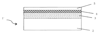
半導体支持基板と、
支持基板上に配置されたトラッピング層と、
を備える高周波用途のための構造に関わる。
トラッピング層は、20℃で、10kOhm.cmよりも大きな、好ましくは50kOhm.cmよりも大きな抵抗率を有し、
トラッピング層と支持基板との間の熱膨張係数の差は、100℃と1200℃との間で、5ppm/k未満であり、
トラッピング層は、20nm未満の、好ましくは10nm未満のサイズの微細構造を備え、
トラッピング層は、多孔性材料または多結晶材料を含み、
トラッピング層は、1から20%の炭素を含む多結晶シリコンを含み、
トラッピング層の厚さは、10μmと50μmとの間、好ましくは20μmと30μmとの間にあり、
支持基板は、以下のグループから選択された材料、すなわち、シリコン、シリコンゲルマニウム、および炭化ケイ素のうちの少なくとも1つを含み、
支持基板の抵抗率は、10Ohm.cmと2000Ohm.cmとの間にある。
活性層は、トラッピング層上に配置され、
活性層は、直接接合によってトラッピング層に転写され、
活性層は、半導体材料から形成され、
活性層は、圧電材料から形成され、
活性層の厚さは、10μmと50μmとの間に含まれ、
誘電体層は、トラッピング層と活性層との間に配置され、
誘電体層は、直接接合によってトラッピング層に転写され、
誘電体層は、10nmと6μmとの間にある。
マイクロ電子デバイスは、スイッチング回路、またはアンテナ適応回路、さらには高周波増幅回路であり、
マイクロ電子デバイスは、複数の能動部品および複数の受動部品を備え、
マイクロ電子デバイスは、少なくとも1つの制御素子、ならびにオーミックコンタクトのマイクロスイッチおよび容量性のマイクロスイッチより構成されている1つのMEMSスイッチング素子を備え、
マイクロ電子デバイスは、体積音波伝搬または表面音波伝搬によって動作する高周波フィルタである。
支持基板上にエピタキシーによる(例えば、ボロン)ドープされたp型シリコンの層の形成であって、900℃と1200℃との間の温度で、前駆体として三塩化シランおよびジボラン(B2H6)を用いて気相堆積法によって行われる、形成と、
その後に、電気化学的な陽極酸化を行うことと、
を含む。
水素および/またはヘリウムの軽イオンをドナー基板に注入し、このドナー基板を、例えば、分子付着によって支持基板2上に順に配置されたトラッピング層3に接合することに基づくSmart Cut(商標)法。その後に、剥離段が、イオン注入深さによって規定された脆弱面のレベルで、ドナー基板(活性層)の表面の微細な層の分離を可能にする。高温熱処理を含むことができる最終段は、最終的に活性層5に、必要とされる結晶質および表面品質を与える。この方法は、数ナノメートルとおよそ1.5μmとの間の厚さの薄い活性層を製造するのに、例えば、シリコン層に、特に適している。
Claims (18)
- 高周波用途のための構造(1、1’、11)であって、
半導体支持基板(2)と、
前記支持基板(2)上に配置されたトラッピング層(3)であって、前記トラッピング層(3)は1から20%の炭素を含む多結晶シリコンを含むトラッピング層(3)と
を備え、
前記トラッピング層(3)は、予め定めた欠陥密度よりも大きな欠陥密度を含み、前記予め定めた欠陥密度は、前記トラッピング層(3)の電気抵抗率が[−20℃;+120℃]の温度範囲にわたって10kohm.cm以上である欠陥密度であることを特徴とする高周波用途のための構造(1、1’、11)。 - 前記トラッピング層(3)は、20℃で10kOhm.cmよりも大きな抵抗率を有することを特徴とする請求項1に記載の高周波用途のための構造(1、1’、11)。
- 前記トラッピング層(3)と前記支持基板(2)との間の熱膨張係数の差は、100℃と1200℃との間で、5ppm/K未満であることを特徴とする請求項1または2に記
載の高周波用途のための構造(1、1’、11)。 - 前記トラッピング層(3)は、20nm未満のサイズの微細構造を含むことを特徴とする請求項1乃至3のいずれか一項に記載の高周波用途のための構造(1、1’、11)。
- 前記トラッピング層(3)は、多孔性材料または多結晶材料を含むことを特徴とする請求項1乃至4のいずれか一項に記載の高周波用途のための構造(1、1’、11)。
- 前記トラッピング層(3)の厚さは、10μmと50μmとの間にあることを特徴とする請求項1乃至5のいずれか一項に記載の高周波用途のための構造(1、1’、11)。
- 前記支持基板(2)は、以下のグループ、すなわち、シリコン、シリコンゲルマニウム、および炭化ケイ素から選択された材料のうちの少なくとも1つを含むことを特徴とする請求項1乃至6のいずれか一項に記載の高周波用途のための構造(1、1’、11)。
- 前記支持基板(2)の抵抗率は、10Ohm.cmと2000Ohm.cmとの間にあることを特徴とする請求項1乃至7のいずれか一項に記載の高周波用途のための構造(1、1’、11)。
- 活性層(5)が前記トラッピング層(3)上に配置されていることを特徴とする請求項1乃至8のいずれか一項に記載の高周波用途のための構造(1、1’、11)。
- 前記活性層(5)は、半導体材料から形成されていることを特徴とする請求項9に記載の高周波用途のための構造(1、1’、11)。
- 前記活性層(5)は、圧電材料から形成されていることを特徴とする請求項9に記載の高周波用途のための構造(1、1’、11)。
- 前記活性層(5)の厚さは、10μmと50μmとの間にあることを特徴とする請求項9乃至11のいずれか一項に記載の高周波用途のための構造(1、1’、11)。
- 誘電体層(4)が前記トラッピング層(3)と前記活性層(5)との間に配置されていることを特徴とする請求項9乃至12のいずれか一項に記載の高周波用途のための構造(1、1’、11)。
- 前記誘電体層(4)は、10nmと6μmとの間にあることを特徴とする請求項13に記載の高周波用途のための構造(1、1’、11)。
- 少なくとも1つのマイクロ電子デバイスが前記活性層(5)上に、または前記活性層(5)内に存在し、前記マイクロ電子デバイスは、スイッチング回路もしくはアンテナ適応回路もしくは高周波電力増幅回路であることを特徴とする請求項9乃至14のいずれか一項に記載の高周波用途のための構造(1、1’、11)。
- 少なくとも1つのマイクロ電子デバイスが前記活性層(5)上に、または前記活性層(5)内に存在し、前記マイクロ電子デバイスは、複数の能動部品および複数の受動部品を備えることを特徴とする請求項9乃至15のいずれか一項に記載の高周波用途のための構造(1、1’、11)。
- 少なくとも1つのマイクロ電子デバイスが前記活性層(5)上に、または前記活性層(
5)内に存在し、前記マイクロ電子デバイスは、少なくとも1つの制御素子、およびオー
ミックコンタクトのマイクロスイッチまたは容量性のマイクロスイッチより構成されてい
る1つのMEMSスイッチング素子を備えることを特徴とする請求項9乃至15のいずれか一項に記載の高周波用途のための構造(1、1’、11)。 - 少なくとも1つのマイクロ電子デバイスが前記活性層(5)上に、または前記活性層(
5)内に存在し、前記マイクロ電子デバイスは、体積音波伝搬または表面音波伝搬によっ
て動作する高周波フィルタであることを特徴とする請求項9乃至14のいずれか一項に記載の高周波用途のための構造(1、1’、11)。
Applications Claiming Priority (3)
| Application Number | Priority Date | Filing Date | Title |
|---|---|---|---|
| FR1402801 | 2014-12-04 | ||
| FR1402801A FR3029682B1 (fr) | 2014-12-04 | 2014-12-04 | Substrat semi-conducteur haute resistivite et son procede de fabrication |
| PCT/FR2015/052494 WO2016087728A1 (fr) | 2014-12-04 | 2015-09-17 | Structure pour applications radiofréquences |
Publications (3)
| Publication Number | Publication Date |
|---|---|
| JP2018501651A JP2018501651A (ja) | 2018-01-18 |
| JP2018501651A5 JP2018501651A5 (ja) | 2018-09-06 |
| JP6612872B2 true JP6612872B2 (ja) | 2019-11-27 |
Family
ID=53039463
Family Applications (1)
| Application Number | Title | Priority Date | Filing Date |
|---|---|---|---|
| JP2017529767A Active JP6612872B2 (ja) | 2014-12-04 | 2015-09-17 | 高周波用途のための構造 |
Country Status (8)
| Country | Link |
|---|---|
| US (1) | US10250282B2 (ja) |
| EP (2) | EP3227905B1 (ja) |
| JP (1) | JP6612872B2 (ja) |
| KR (1) | KR102395398B1 (ja) |
| CN (1) | CN107004572B (ja) |
| FR (1) | FR3029682B1 (ja) |
| SG (1) | SG11201704516QA (ja) |
| WO (1) | WO2016087728A1 (ja) |
Families Citing this family (24)
| Publication number | Priority date | Publication date | Assignee | Title |
|---|---|---|---|---|
| FR3037438B1 (fr) | 2015-06-09 | 2017-06-16 | Soitec Silicon On Insulator | Procede de fabrication d'un element semi-conducteur comprenant une couche de piegeage de charges |
| US10523178B2 (en) | 2015-08-25 | 2019-12-31 | Avago Technologies International Sales Pte. Limited | Surface acoustic wave (SAW) resonator |
| US10530327B2 (en) * | 2015-08-25 | 2020-01-07 | Avago Technologies International Sales Pte. Limited | Surface acoustic wave (SAW) resonator |
| US10541667B2 (en) * | 2015-08-25 | 2020-01-21 | Avago Technologies International Sales Pte. Limited | Surface acoustic wave (SAW) resonator having trap-rich region |
| US10181428B2 (en) * | 2015-08-28 | 2019-01-15 | Skyworks Solutions, Inc. | Silicon on porous silicon |
| EP3144958B1 (en) | 2015-09-17 | 2021-03-17 | Soitec | Structure for radiofrequency applications and process for manufacturing such a structure |
| WO2017145954A1 (ja) * | 2016-02-25 | 2017-08-31 | 日本ゼオン株式会社 | 熱伝導シートおよびその製造方法、ならびに放熱装置 |
| FR3053532B1 (fr) * | 2016-06-30 | 2018-11-16 | Soitec | Structure hybride pour dispositif a ondes acoustiques de surface |
| FR3058561B1 (fr) * | 2016-11-04 | 2018-11-02 | Soitec | Procede de fabrication d'un element semi-conducteur comprenant un substrat hautement resistif |
| FR3062238A1 (fr) * | 2017-01-26 | 2018-07-27 | Soitec | Support pour une structure semi-conductrice |
| FR3062517B1 (fr) * | 2017-02-02 | 2019-03-15 | Soitec | Structure pour application radiofrequence |
| US10784348B2 (en) | 2017-03-23 | 2020-09-22 | Qualcomm Incorporated | Porous semiconductor handle substrate |
| US11063117B2 (en) * | 2017-04-20 | 2021-07-13 | Taiwan Semiconductor Manufacturing Co., Ltd. | Semiconductor device structure having carrier-trapping layers with different grain sizes |
| FR3067517B1 (fr) | 2017-06-13 | 2019-07-12 | Commissariat A L'energie Atomique Et Aux Energies Alternatives | Substrat soi compatible avec les technologies rfsoi et fdsoi |
| FR3079662B1 (fr) * | 2018-03-30 | 2020-02-28 | Soitec | Substrat pour applications radiofrequences et procede de fabrication associe |
| JP7230297B2 (ja) * | 2018-07-05 | 2023-03-01 | ソイテック | 集積された高周波デバイスのための基板及びそれを製造するための方法 |
| FR3098642B1 (fr) * | 2019-07-12 | 2021-06-11 | Soitec Silicon On Insulator | procédé de fabrication d'une structure comprenant une couche mince reportée sur un support muni d’une couche de piégeage de charges |
| CN113629182A (zh) * | 2020-05-08 | 2021-11-09 | 济南晶正电子科技有限公司 | 一种tc-saw复合衬底及其制备方法 |
| CN111884616B (zh) * | 2020-07-23 | 2021-04-13 | 中国科学院上海微系统与信息技术研究所 | 一种衬底基板/压电材料薄膜结构及其制备方法和应用 |
| CN112260660B (zh) * | 2020-10-21 | 2023-03-03 | 济南晶正电子科技有限公司 | 一种复合基底、复合薄膜及其制备方法 |
| FR3117668B1 (fr) | 2020-12-16 | 2022-12-23 | Commissariat Energie Atomique | Structure amelioree de substrat rf et procede de realisation |
| CN112750686B (zh) * | 2020-12-30 | 2021-12-07 | 济南晶正电子科技有限公司 | 一种多层衬底、电子元器件及多层衬底制备方法 |
| WO2023232562A1 (fr) * | 2022-06-02 | 2023-12-07 | Soitec | Procédé de fabrication d'un dispositif à ondes élastiques de surface |
| FR3136325A1 (fr) * | 2022-06-02 | 2023-12-08 | Soitec | Dispositif a ondes elastiques de surface |
Family Cites Families (8)
| Publication number | Priority date | Publication date | Assignee | Title |
|---|---|---|---|---|
| US5637883A (en) * | 1995-02-27 | 1997-06-10 | The United States Of America As Represented By The Secretary Of The Navy | Optically addressed spatial light modulator using an intrinsic semiconductor active material and high resistivity cladding layers |
| KR20060118437A (ko) * | 2003-09-26 | 2006-11-23 | 위니베르시트카솔리끄드루뱅 | 저항손을 감소시키는 다층 반도체 구조의 제조 방법 |
| JP4983010B2 (ja) * | 2005-11-30 | 2012-07-25 | 富士通株式会社 | 圧電素子及びその製造方法 |
| JP2009231376A (ja) * | 2008-03-19 | 2009-10-08 | Shin Etsu Handotai Co Ltd | Soiウェーハ及び半導体デバイスならびにsoiウェーハの製造方法 |
| US8536021B2 (en) * | 2010-12-24 | 2013-09-17 | Io Semiconductor, Inc. | Trap rich layer formation techniques for semiconductor devices |
| JP6004285B2 (ja) * | 2010-12-24 | 2016-10-05 | クォルコム・インコーポレイテッド | 半導体デバイスのためのトラップリッチ層 |
| FR2973158B1 (fr) * | 2011-03-22 | 2014-02-28 | Soitec Silicon On Insulator | Procédé de fabrication d'un substrat de type semi-conducteur sur isolant pour applications radiofréquences |
| KR101876579B1 (ko) * | 2012-09-13 | 2018-07-10 | 매그나칩 반도체 유한회사 | 전력용 반도체 소자 및 그 소자의 제조 방법 |
-
2014
- 2014-12-04 FR FR1402801A patent/FR3029682B1/fr active Active
-
2015
- 2015-09-17 EP EP15788467.7A patent/EP3227905B1/fr active Active
- 2015-09-17 US US15/531,976 patent/US10250282B2/en active Active
- 2015-09-17 WO PCT/FR2015/052494 patent/WO2016087728A1/fr active Application Filing
- 2015-09-17 KR KR1020177015538A patent/KR102395398B1/ko active IP Right Grant
- 2015-09-17 EP EP21170134.7A patent/EP3872839A1/fr active Pending
- 2015-09-17 CN CN201580065277.5A patent/CN107004572B/zh active Active
- 2015-09-17 JP JP2017529767A patent/JP6612872B2/ja active Active
- 2015-09-17 SG SG11201704516QA patent/SG11201704516QA/en unknown
Also Published As
| Publication number | Publication date |
|---|---|
| CN107004572B (zh) | 2020-05-22 |
| CN107004572A (zh) | 2017-08-01 |
| EP3227905B1 (fr) | 2021-08-18 |
| KR20170091627A (ko) | 2017-08-09 |
| US20170331501A1 (en) | 2017-11-16 |
| JP2018501651A (ja) | 2018-01-18 |
| FR3029682B1 (fr) | 2017-12-29 |
| US10250282B2 (en) | 2019-04-02 |
| EP3227905A1 (fr) | 2017-10-11 |
| EP3872839A1 (fr) | 2021-09-01 |
| WO2016087728A1 (fr) | 2016-06-09 |
| FR3029682A1 (fr) | 2016-06-10 |
| KR102395398B1 (ko) | 2022-05-10 |
| SG11201704516QA (en) | 2017-07-28 |
Similar Documents
| Publication | Publication Date | Title |
|---|---|---|
| JP6612872B2 (ja) | 高周波用途のための構造 | |
| JP2018501651A5 (ja) | ||
| JP6643316B2 (ja) | 無線周波アプリケーションの構造 | |
| JP7053502B2 (ja) | 無線周波数用途のための構造 | |
| KR102520751B1 (ko) | 무선 주파수 응용들을 위한 구조 | |
| KR102652250B1 (ko) | 집적 무선 주파수 디바이스를 위한 기판 및 이를 제조하기 위한 방법 | |
| KR20220025892A (ko) | Rf 응용들을 위한 매립된 다공성 층을 포함하는 반도체 구조물 | |
| WO2023162448A1 (ja) | 高周波デバイス用基板、及びその製造方法 | |
| TWI751352B (zh) | 集成射頻元件用底材及其製作方法 | |
| CN116783683A (zh) | 适用于射频应用的由硅制成的支撑衬底及相关制造方法 |
Legal Events
| Date | Code | Title | Description |
|---|---|---|---|
| A521 | Request for written amendment filed |
Free format text: JAPANESE INTERMEDIATE CODE: A523 Effective date: 20180725 |
|
| A621 | Written request for application examination |
Free format text: JAPANESE INTERMEDIATE CODE: A621 Effective date: 20180725 |
|
| A977 | Report on retrieval |
Free format text: JAPANESE INTERMEDIATE CODE: A971007 Effective date: 20190514 |
|
| A131 | Notification of reasons for refusal |
Free format text: JAPANESE INTERMEDIATE CODE: A131 Effective date: 20190521 |
|
| A521 | Request for written amendment filed |
Free format text: JAPANESE INTERMEDIATE CODE: A523 Effective date: 20190821 |
|
| TRDD | Decision of grant or rejection written | ||
| A01 | Written decision to grant a patent or to grant a registration (utility model) |
Free format text: JAPANESE INTERMEDIATE CODE: A01 Effective date: 20191001 |
|
| A61 | First payment of annual fees (during grant procedure) |
Free format text: JAPANESE INTERMEDIATE CODE: A61 Effective date: 20191031 |
|
| R150 | Certificate of patent or registration of utility model |
Ref document number: 6612872 Country of ref document: JP Free format text: JAPANESE INTERMEDIATE CODE: R150 |
|
| R250 | Receipt of annual fees |
Free format text: JAPANESE INTERMEDIATE CODE: R250 |
|
| R250 | Receipt of annual fees |
Free format text: JAPANESE INTERMEDIATE CODE: R250 |