JP6607441B2 - Lead frame and manufacturing method thereof, and semiconductor device and manufacturing method thereof - Google Patents
Lead frame and manufacturing method thereof, and semiconductor device and manufacturing method thereof Download PDFInfo
- Publication number
- JP6607441B2 JP6607441B2 JP2015166792A JP2015166792A JP6607441B2 JP 6607441 B2 JP6607441 B2 JP 6607441B2 JP 2015166792 A JP2015166792 A JP 2015166792A JP 2015166792 A JP2015166792 A JP 2015166792A JP 6607441 B2 JP6607441 B2 JP 6607441B2
- Authority
- JP
- Japan
- Prior art keywords
- lead
- terminal portion
- terminal
- lead portion
- die pad
- Prior art date
- Legal status (The legal status is an assumption and is not a legal conclusion. Google has not performed a legal analysis and makes no representation as to the accuracy of the status listed.)
- Active
Links
Images


Classifications
-
- H—ELECTRICITY
- H01—ELECTRIC ELEMENTS
- H01L—SEMICONDUCTOR DEVICES NOT COVERED BY CLASS H10
- H01L2224/00—Indexing scheme for arrangements for connecting or disconnecting semiconductor or solid-state bodies and methods related thereto as covered by H01L24/00
- H01L2224/01—Means for bonding being attached to, or being formed on, the surface to be connected, e.g. chip-to-package, die-attach, "first-level" interconnects; Manufacturing methods related thereto
- H01L2224/42—Wire connectors; Manufacturing methods related thereto
- H01L2224/47—Structure, shape, material or disposition of the wire connectors after the connecting process
- H01L2224/48—Structure, shape, material or disposition of the wire connectors after the connecting process of an individual wire connector
- H01L2224/4805—Shape
- H01L2224/4809—Loop shape
- H01L2224/48091—Arched
-
- H—ELECTRICITY
- H01—ELECTRIC ELEMENTS
- H01L—SEMICONDUCTOR DEVICES NOT COVERED BY CLASS H10
- H01L2224/00—Indexing scheme for arrangements for connecting or disconnecting semiconductor or solid-state bodies and methods related thereto as covered by H01L24/00
- H01L2224/01—Means for bonding being attached to, or being formed on, the surface to be connected, e.g. chip-to-package, die-attach, "first-level" interconnects; Manufacturing methods related thereto
- H01L2224/42—Wire connectors; Manufacturing methods related thereto
- H01L2224/47—Structure, shape, material or disposition of the wire connectors after the connecting process
- H01L2224/48—Structure, shape, material or disposition of the wire connectors after the connecting process of an individual wire connector
- H01L2224/481—Disposition
- H01L2224/48151—Connecting between a semiconductor or solid-state body and an item not being a semiconductor or solid-state body, e.g. chip-to-substrate, chip-to-passive
- H01L2224/48221—Connecting between a semiconductor or solid-state body and an item not being a semiconductor or solid-state body, e.g. chip-to-substrate, chip-to-passive the body and the item being stacked
- H01L2224/48245—Connecting between a semiconductor or solid-state body and an item not being a semiconductor or solid-state body, e.g. chip-to-substrate, chip-to-passive the body and the item being stacked the item being metallic
- H01L2224/48247—Connecting between a semiconductor or solid-state body and an item not being a semiconductor or solid-state body, e.g. chip-to-substrate, chip-to-passive the body and the item being stacked the item being metallic connecting the wire to a bond pad of the item
-
- H—ELECTRICITY
- H01—ELECTRIC ELEMENTS
- H01L—SEMICONDUCTOR DEVICES NOT COVERED BY CLASS H10
- H01L2224/00—Indexing scheme for arrangements for connecting or disconnecting semiconductor or solid-state bodies and methods related thereto as covered by H01L24/00
- H01L2224/73—Means for bonding being of different types provided for in two or more of groups H01L2224/10, H01L2224/18, H01L2224/26, H01L2224/34, H01L2224/42, H01L2224/50, H01L2224/63, H01L2224/71
- H01L2224/732—Location after the connecting process
- H01L2224/73251—Location after the connecting process on different surfaces
- H01L2224/73265—Layer and wire connectors
-
- H—ELECTRICITY
- H01—ELECTRIC ELEMENTS
- H01L—SEMICONDUCTOR DEVICES NOT COVERED BY CLASS H10
- H01L2924/00—Indexing scheme for arrangements or methods for connecting or disconnecting semiconductor or solid-state bodies as covered by H01L24/00
- H01L2924/15—Details of package parts other than the semiconductor or other solid state devices to be connected
- H01L2924/181—Encapsulation
Description
本発明は、リードフレームおよびその製造方法、ならびに半導体装置およびその製造方法に関する。 The present invention relates to a lead frame and a manufacturing method thereof, and a semiconductor device and a manufacturing method thereof.
近年、基板に実装される半導体装置の小型化および薄型化が要求されてきている。このような要求に対応すべく、従来、リードフレームを用い、その搭載面に搭載した半導体素子を封止樹脂によって封止するとともに、裏面側にリードの一部分を露出させて構成された、いわゆるQFN(Quad Flat Non-lead)タイプの半導体装置が種々提案されている。 In recent years, it has been required to reduce the size and thickness of a semiconductor device mounted on a substrate. In order to meet such demands, conventionally, a lead frame is used, and a semiconductor element mounted on the mounting surface is sealed with a sealing resin, and a part of the lead is exposed on the back surface side, so-called QFN. Various (Quad Flat Non-lead) type semiconductor devices have been proposed.
しかしながら、従来一般的な構造からなるQFNの場合、端子数が増加するにしたがってパッケージが大きくなるため、実装信頼性を確保することが難しくなるという課題があった。これに対して、多ピン化されたQFNを実現するための技術として、外部端子を2列に配列したパッケージの開発が進められている(例えば特許文献1)。このようなパッケージは、DR−QFN(Dual Row QFN)パッケージともよばれている。 However, in the case of a QFN having a conventional general structure, since the package becomes larger as the number of terminals increases, there is a problem that it is difficult to ensure mounting reliability. On the other hand, as a technique for realizing a multi-pin QFN, development of a package in which external terminals are arranged in two rows is underway (for example, Patent Document 1). Such a package is also called a DR-QFN (Dual Row QFN) package.
近年、DR−QFNパッケージを生産するにあたり、チップサイズを変更することなく、リード部の数(ピン数)を増やすことが求められてきている。これに対して、従来、ピン数を増やすために、パッケージサイズを大きくする手法がとられてきた。しかしながら、パッケージを電子機器へ搭載する上での制約があるため、パッケージサイズを大きくすることには限界がある。 In recent years, in producing a DR-QFN package, it has been required to increase the number of leads (number of pins) without changing the chip size. On the other hand, conventionally, in order to increase the number of pins, a method of increasing the package size has been taken. However, there is a limit in increasing the package size due to restrictions on mounting the package on the electronic device.
また、外部端子を3列に配列したパッケージとして、例えば特許文献2に記載されたものが知られている。しかしながら、特許文献2のパッケージにおいては、各外部端子が支持リードの垂直方向に一直線上に並んでいるため、端子間の距離を十分に確保できないおそれがある。 As a package in which external terminals are arranged in three rows, for example, a package described in Patent Document 2 is known. However, in the package of Patent Document 2, since the external terminals are arranged in a straight line in the vertical direction of the support leads, there is a possibility that a sufficient distance between the terminals cannot be secured.
本発明はこのような点を考慮してなされたものであり、外部と接続される端子部の数(ピン数)を増やすとともに、各端子部間の距離を十分に確保することが可能な、リードフレームおよびその製造方法、ならびに半導体装置およびその製造方法を提供することを目的とする。 The present invention has been made in consideration of such points, and while increasing the number of terminal portions (number of pins) connected to the outside, it is possible to sufficiently secure the distance between each terminal portion. An object of the present invention is to provide a lead frame and a manufacturing method thereof, and a semiconductor device and a manufacturing method thereof.
本発明は、半導体装置用のリードフレームであって、半導体素子が搭載されるダイパッドと、前記ダイパッド周囲に設けられ、それぞれ第1端子部を含む複数の第1リード部と、前記ダイパッド周囲に設けられ、それぞれ第2端子部を含む複数の第2リード部と、前記ダイパッド周囲に設けられ、それぞれ第3端子部を含む複数の第3リード部とを備え、前記第1リード部、前記第2リード部および前記第3リード部は、それぞれ支持リードに支持され、前記第1リード部の前記第1端子部は、前記第2リード部の前記第2端子部よりも外側に位置するとともに、当該第1リード部に隣接する第2リード部の前記第2端子部に対して前記支持リードの長手方向にずれて配置され、前記第2リード部の前記第2端子部は、前記第3リード部の前記第3端子部よりも外側に位置するとともに、当該第2リード部に隣接する第3リード部の前記第3端子部に対して前記支持リードの長手方向にずれて配置されていることを特徴とするリードフレームである。 The present invention is a lead frame for a semiconductor device, which is provided around a die pad on which a semiconductor element is mounted, a plurality of first lead portions provided around the die pad, each including a first terminal portion, and the die pad. A plurality of second lead portions each including a second terminal portion; and a plurality of third lead portions provided around the die pad and each including a third terminal portion, wherein the first lead portion and the second lead portion are provided. The lead portion and the third lead portion are respectively supported by support leads, and the first terminal portion of the first lead portion is located outside the second terminal portion of the second lead portion, and The second lead portion adjacent to the first lead portion is arranged to be shifted in the longitudinal direction of the support lead with respect to the second terminal portion, and the second terminal portion of the second lead portion is arranged to be the third lead portion. Before It is located outside the third terminal portion, and is arranged so as to be shifted in the longitudinal direction of the support lead with respect to the third terminal portion of the third lead portion adjacent to the second lead portion. Lead frame.
本発明は、前記第1リード部、前記第2リード部および前記第3リード部は、前記支持リードに沿ってこの順番に繰り返し配置されていることを特徴とするリードフレームである。 The present invention is the lead frame characterized in that the first lead portion, the second lead portion, and the third lead portion are repeatedly arranged in this order along the support lead.
本発明は、前記第1リード部の前記第1端子部の中心と、当該第1リード部に隣接する第2リード部の前記第2端子部の中心と、当該第2リード部に隣接する第3リード部の前記第3端子部の中心とが一直線上に並んでいることを特徴とするリードフレームである。 The present invention provides the center of the first terminal portion of the first lead portion, the center of the second terminal portion of the second lead portion adjacent to the first lead portion, and the second adjacent to the second lead portion. The lead frame is characterized in that the center of the third terminal portion of the three lead portions is aligned on a straight line.
本発明は、前記第1端子部、前記第2端子部および前記第3端子部の外周は、それぞれ平面円弧形状部分を有することを特徴とするリードフレームである。 The present invention is the lead frame characterized in that outer circumferences of the first terminal portion, the second terminal portion, and the third terminal portion each have a planar arc-shaped portion.
本発明は、前記複数の第1リード部、前記複数の第2リード部および前記複数の第3リード部は、前記支持リードの長手方向中央部を中心として線対称に配置されていることを特徴とするリードフレームである。 The present invention is characterized in that the plurality of first lead portions, the plurality of second lead portions, and the plurality of third lead portions are arranged symmetrically with respect to a longitudinal center portion of the support lead. The lead frame.
本発明は、前記第1リード部、前記第2リード部および前記第3リード部は、それぞれ前記第1端子部、前記第2端子部および前記第3端子部から前記ダイパッド側に延びる内部領域を有し、前記内部領域のうち少なくとも前記第1端子部、前記第2端子部又は前記第3端子部との連結部分は、それぞれ前記支持リードに対して垂直な方向に延びていることを特徴とするリードフレームである。 In the present invention, the first lead portion, the second lead portion, and the third lead portion have internal regions extending from the first terminal portion, the second terminal portion, and the third terminal portion to the die pad side, respectively. And at least a connecting portion of the inner region with the first terminal portion, the second terminal portion, or the third terminal portion extends in a direction perpendicular to the support lead. Lead frame.
本発明は、前記ダイパッドは、吊りリードを介して前記支持リードに連結支持されており、前記複数の第1リード部、前記複数の第2リード部および前記複数の第3リード部のうち、前記支持リードの長手方向端部近傍に位置するリード部は、前記吊りリードに連結されていることを特徴とするリードフレームである。 In the present invention, the die pad is connected to and supported by the support lead via a suspension lead, and among the plurality of first lead portions, the plurality of second lead portions, and the plurality of third lead portions, A lead frame located in the vicinity of the longitudinal end of the support lead is connected to the suspension lead.
本発明は、前記ダイパッドの表面外周に沿って、めっき部が形成されていることを特徴とするリードフレームである。 The present invention is the lead frame characterized in that a plating portion is formed along the outer periphery of the surface of the die pad.
本発明は、前記ダイパッドと、前記第1リード部、前記第2リード部および前記第3リード部との間に接続バーが配置され、前記接続バーに、複数の第4端子部が連結されていることを特徴とするリードフレームである。 In the present invention, a connection bar is disposed between the die pad and the first lead portion, the second lead portion, and the third lead portion, and a plurality of fourth terminal portions are coupled to the connection bar. It is a lead frame characterized by being.
本発明は、前記ダイパッドの裏面外周に沿って薄肉部が形成されていることを特徴とするリードフレームである。 The present invention is the lead frame characterized in that a thin portion is formed along the outer periphery of the back surface of the die pad.
本発明は、前記ダイパッドの表面に、前記ダイパッドと前記半導体素子とを固定する接着剤の流れを止める流れ止め凹部が形成されていることを特徴とするリードフレームである。 The present invention is the lead frame, wherein a flow stop recess for stopping a flow of an adhesive for fixing the die pad and the semiconductor element is formed on a surface of the die pad.
本発明は、半導体装置であって、ダイパッドと、前記ダイパッド周囲に設けられ、それぞれ第1端子部を含む複数の第1リード部と、前記ダイパッド周囲に設けられ、それぞれ第2端子部を含む複数の第2リード部と、前記ダイパッド周囲に設けられ、それぞれ第3端子部を含む複数の第3リード部と、前記ダイパッド上に搭載された半導体素子と、前記半導体素子と、前記第1リード部、前記第2リード部および前記第3リード部とをそれぞれ電気的に接続する導電部材と、前記ダイパッドと、前記第1リード部と、前記第2リード部と、前記第3リード部と、前記半導体素子と、前記導電部材とを封止する封止樹脂とを備え、前記第1リード部の前記第1端子部は、前記第2リード部の前記第2端子部よりも外側に位置するとともに、当該第1リード部に隣接する第2リード部の前記第2端子部に対して前記封止樹脂の周縁方向にずれて配置され、前記第2リード部の前記第2端子部は、前記第3リード部の前記第3端子部よりも外側に位置するとともに、当該第2リード部に隣接する第3リード部の前記第3端子部に対して前記封止樹脂の周縁方向にずれて配置されていることを特徴とする半導体装置である。 The present invention is a semiconductor device, a die pad, a plurality of first lead portions provided around the die pad, each including a first terminal portion, and a plurality provided respectively around the die pad, each including a second terminal portion. A second lead portion, a plurality of third lead portions provided around the die pad, each including a third terminal portion, a semiconductor element mounted on the die pad, the semiconductor element, and the first lead portion , A conductive member that electrically connects the second lead part and the third lead part, the die pad, the first lead part, the second lead part, the third lead part, And a sealing resin that seals the semiconductor element and the conductive member, and the first terminal portion of the first lead portion is positioned outside the second terminal portion of the second lead portion. This The second lead portion adjacent to the first lead portion is disposed to be shifted in the peripheral direction of the sealing resin with respect to the second terminal portion of the second lead portion, and the second terminal portion of the second lead portion is the third lead Is located outside of the third terminal portion of the portion, and is displaced in the peripheral direction of the sealing resin with respect to the third terminal portion of the third lead portion adjacent to the second lead portion. This is a semiconductor device.
本発明は、前記リードフレームの製造方法であって、金属基板を準備する工程と、前記金属基板をエッチング加工することにより、前記金属基板に前記ダイパッド、前記複数の第1リード部、前記複数の第2リード部および前記複数の第3リード部を形成する工程とを備えたことを特徴とするリードフレームの製造方法である。 The present invention is a method for manufacturing the lead frame, comprising: preparing a metal substrate; and etching the metal substrate to form the die pad, the plurality of first lead portions, and the plurality of the plurality of first lead portions on the metal substrate. Forming a second lead portion and the plurality of third lead portions.
本発明は、半導体装置の製造方法であって、前記リードフレームを準備する工程と、前記リードフレームの前記ダイパッド上に前記半導体素子を搭載する工程と、前記半導体素子と、前記第1リード部、前記第2リード部および前記第3リード部とを導電部材により電気的に接続する工程と、前記ダイパッドと、前記複数の第1リード部と、前記複数の第2リード部と、前記複数の第3リード部と、前記半導体素子と、前記導電部材とを封止樹脂により封止する工程とを備えたことを特徴とする半導体装置の製造方法である。 The present invention is a method of manufacturing a semiconductor device, the step of preparing the lead frame, the step of mounting the semiconductor element on the die pad of the lead frame, the semiconductor element, the first lead portion, Electrically connecting the second lead portion and the third lead portion with a conductive member, the die pad, the plurality of first lead portions, the plurality of second lead portions, and the plurality of first leads. A method of manufacturing a semiconductor device, comprising: a step of sealing three lead portions, the semiconductor element, and the conductive member with a sealing resin.
本発明によれば、外部と接続される端子部の数(ピン数)を増やすとともに、各端子部間の距離を十分に確保することができる。 ADVANTAGE OF THE INVENTION According to this invention, while increasing the number of the terminal parts connected to the exterior (pin number), the distance between each terminal part is fully securable.
以下、本発明の一実施の形態について、図1乃至図8を参照して説明する。なお、以下の各図において、同一部分には同一の符号を付しており、一部詳細な説明を省略する場合がある。 Hereinafter, an embodiment of the present invention will be described with reference to FIGS. Note that, in the following drawings, the same portions are denoted by the same reference numerals, and some detailed description may be omitted.
リードフレームの構成
まず、図1乃至図4により、本実施の形態によるリードフレームの概略について説明する。図1乃至図4は、本実施の形態によるリードフレームを示す図である。
Construction of the lead frame initially, to FIG. 1 to FIG. 4, the outline of the lead frame according to the present embodiment. 1 to 4 are views showing a lead frame according to the present embodiment.
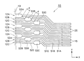
図1乃至図3に示すように、リードフレーム10は、半導体素子21(後述)を搭載する平面矩形状のダイパッド11と、ダイパッド11周囲に設けられ、半導体素子21と外部回路(図示せず)とを接続する複数の細長いリード部12A、12B、12Cとを備えている。
As shown in FIGS. 1 to 3, the
図1において、符号10aは単位リードフレームを示しており、各単位リードフレーム10aは、それぞれ半導体装置20(後述)に対応している。また、各単位リードフレーム10aは、支持リード(支持部材)13を介して互いに連結されている。この支持リード13は、ダイパッド11とリード部12A、12B、12Cとを支持するものであり、X方向、およびX方向に垂直なY方向に沿ってそれぞれ延びている。なお、ダイパッド11の四隅には吊りリード14が連結されており、ダイパッド11は、この4本の吊りリード14を介して支持リード13に連結支持されている。
In FIG. 1, reference numeral 10a denotes a unit lead frame, and each unit lead frame 10a corresponds to a semiconductor device 20 (described later). The unit lead frames 10 a are connected to each other through support leads (support members) 13. The support leads 13 support the
次に、リード部12A、12B、12Cの構成について説明する。なお、リード部12A、12B、12Cのことを、それぞれ第1リード部12A、第2リード部12B、第3リード部12Cともいう。
Next, the configuration of the
第1リード部12Aは、それぞれ第1端子部53Aと、第1端子部53Aに連結された内部領域(インナーリード)51Aとを有している。このうち内部領域51Aは、第1端子部53Aから内側(ダイパッド11側)に向けて延びるとともに、その先端部がダイパッド11から離間して配置されている。また第1端子部53Aは、支持リード13に対して直接連結されている。
The
第2リード部12Bは、それぞれ第2端子部53Bと、第2端子部53Bに連結された内部領域(インナーリード)51Bと、第2端子部53Bに連結された外部領域(接続リード)52Bとを有している。このうち内部領域51Bは、第2端子部53Bから内側(ダイパッド11側)に向けて延びるとともに、その先端部がダイパッド11から離間して配置されている。また外部領域52Bは、第2端子部53Bから外側(支持リード13側)に向けて延びるとともに、支持リード13に連結されている。
The
第3リード部12Cは、それぞれ第3端子部53Cと、第3端子部53Cに連結された内部領域(インナーリード)51Cと、第3端子部53Cに連結された外部領域(接続リード)52Cとを有している。このうち内部領域51Cは、第3端子部53Cから内側(ダイパッド11側)に向けて延びるとともに、その先端部がダイパッド11から離間して配置されている。また外部領域52Cは、第3端子部53Cから外側(支持リード13側)に向けて延びるとともに、支持リード13に連結されている。
The
リード部12A、12B、12Cの内部領域51A、51B、51Cの先端部(ダイパッド11側端部)の表面には、それぞれ内部端子15が形成されている。この内部端子15は、後述するようにボンディングワイヤ22を介して半導体素子21に電気的に接続される領域となっている。このため、内部端子15上には、ボンディングワイヤ22との密着性を向上させるめっき部25が設けられている。また、リード部12A、12B、12Cの各内部端子15は、ダイパッド11の辺に平行な直線に沿って配置されている。これにより、ボンディングワイヤ22の長さを略均一にすることができ、ボンディング作業の効率を高めることができる。
互いに隣接するリード部12A、12Bと、リード部12B、12Cと、リード部12C、12Aとは、それぞれ半導体装置20(後述)の製造後に互いに電気的に絶縁される形状となっている。また、各リード部12A、12B、12Cは、半導体装置20の製造後にダイパッド11と電気的に絶縁される形状となっている。この端子部53A、53B、53Cの裏面には、それぞれ外部の実装基板(図示せず)に電気的に接続される外部端子17A、17B、17Cが形成されている。各外部端子17A、17B、17Cは、半導体装置20(後述)の製造後に、それぞれ半導体装置20から外方に露出するようになっている。
The
リード部12A、12B、12Cの内部領域51A、51B、51Cおよび外部領域52B、52Cは、それぞれ裏面側(半導体素子21を搭載する面の反対側)からハーフエッチングにより薄肉に形成されている。一方、端子部53A、53B、53Cは、ハーフエッチングされることなく、ダイパッド11および支持リード13と同一の厚みを有している。このように、内部領域51A、51B、51Cおよび外部領域52B、52Cの厚みを端子部53A、53B、53Cの厚みよりも薄くすることにより、幅の狭いリード部12A、12B、12Cを精度良く形成することができ、小型でピン数の多い半導体装置20を得ることができる。なお、ハーフエッチングとは、被エッチング材料をその厚み方向に途中までエッチングすることをいう。なお、本実施の形態において、第1リード部12Aは外部領域を有していないが、これに限らず、第1リード部12Aが、裏面側からハーフエッチングにより薄肉に形成された外部領域を有していても良い。
The
図1および図3に示すように、第1リード部12A、第2リード部12Bおよび第3リード部12Cは、それぞれ支持リード13に支持されるとともに、支持リード13に沿ってこの順番に繰り返し配置されている。すなわち、本実施の形態において、支持リード13の長手方向端部側から長手方向中央部側に向けて、第1リード部12A、第2リード部12Bおよび第3リード部12Cがこの順に繰り返し配列されている。
As shown in FIGS. 1 and 3, the first lead portion 12 </ b> A, the second lead portion 12 </ b> B, and the third lead portion 12 </ b> C are supported by the support leads 13 and are repeatedly arranged in this order along the support leads 13. Has been. That is, in the present embodiment, the
なお、支持リード13の長手方向両端部には、それぞれ第2リード部12Bおよび第3リード部12Cが設けられている。これら一対のリード部12B、12Cは、支持リード13からダイパッド11側に延びて、それぞれ第2端子部53Bおよび第3端子部53Cで終端している。すなわち、これらのリード部12B、12Cは、他のリード部12B、12Cと異なり、内部領域51B、51Cを有していない。これにより、ダイパッド11の角部近傍で内部領域51A、51B、51Cが集中しすぎてこれらが接近してしまう不具合を防止するとともに、半導体装置20(後述)の角部近傍の領域を有効に利用することができる。なお、支持リード13の長手方向端部に、内部領域51Aを有していない、第1端子部53Aで終端する第1リード部12Aを設けても良い。
A
また、支持リード13の長手方向中央部には、第1リード部12Aが設けられている。
この中央の第1リード部12Aから、支持リード13の長手方向両端部側に向けて、第3リード部12C、第2リード部12Bおよび第1リード部12Aがこの順に繰り返し配列されている。この場合、支持リード13に支持された複数の第1リード部12A、複数の第2リード部12Bおよび複数の第3リード部12Cが、支持リード13の長手方向中央部を中心として線対称に配置されている。具体的には、中央の第1リード部12Aを中心として、その両側のリード部12A、12B、12Cの形状及び配置関係の両方が線対称となっている。これにより、端子部53A、53B、53Cをバランス良く配置することができ、半導体装置20の設計や製造を容易にすることができる。
In addition, a first lead portion 12 </ b> A is provided at the center in the longitudinal direction of the
The
図1に示すように、複数のリード部12A、12B、12Cの端子部53A、53B、53Cは、平面から見て千鳥状に配置されている。この場合、複数の端子部53A、53B、53Cは、それぞれX方向又はY方向のいずれかに対して平行な直線に沿って、3列に配列されている。すなわち、複数の端子部53A、53B、53Cは、それぞれ直線LA、LB、LCに沿って配列されている。なお、直線LA、LB間の距離D1と、直線LB、LC間の距離D2とは、互いに等しくなっている(D1=D2)。
As shown in FIG. 1, the
さらに、第1リード部12Aの第1端子部53Aは、第2リード部12Bの第2端子部53Bよりも外側(支持リード13側)に位置している。また、第1端子部53Aは、その隣接する第2端子部53Bに対して支持リード13の長手方向にずれて配置されている。なお、「第1端子部53Aが第2端子部53Bに対してずれている」とは、第1端子部53Aの中心が第2端子部53Bの中心に対してずれていることをいう。また、「長手方向にずれて配置されている」とは、「長手方向に沿って、異なる位置に配置されている」ことをいう。例えば、支持リード13の長手方向がY方向に平行である場合、第1端子部53Aの中心と第2端子部53Bの中心とがY方向に異なる位置にあることをいう。
Furthermore, the first
同様に、第2リード部12Bの第2端子部53Bは、第3リード部12Cの第3端子部53Cよりも外側(支持リード13側)に位置している。また、第2端子部53Bは、その隣接する第3端子部53Cに対して支持リード13の長手方向にずれて配置されている。さらに、第3端子部53Cは、その隣接する第1端子部53Aに対して支持リード13の長手方向にずれて配置されている。
Similarly, the second
これにより、リード部12A、12B、12Cの端子部53A、53B、53C間のピッチが確保されるので、端子部53A、53B、53Cが、隣接するリード部12A、12B、12Cに接触する不具合が防止される。
Thereby, since the pitch between the
次に、図4を参照して、各リード部12A、12B、12Cの構成について更に説明する。
Next, with reference to FIG. 4, the structure of each
図4に示すように、リード部12A、12B、12Cの内部領域51A、51B、51Cは、平面から見て支持リード13に対して垂直な方向に延びる垂直領域51pと、支持リード13に対して傾斜して(非垂直に)延びる傾斜領域51tとを有している。図4に示すように、各内部領域51A、51B、51Cは、それぞれ複数の垂直領域51pと、複数の傾斜領域51tとを有していても良い(例えば図4中、最も上方の第1リード部12A)。また、各内部領域51A、51B、51Cは、それぞれ複数の垂直領域51pと、1つの傾斜領域51tとを有していても良い(例えば図4中、最も下方の第3リード部12C)。さらに、内部端子15は、垂直領域51pに設けられていても良く(図4参照)、傾斜領域51tに設けられていても良い(図3参照)。
As shown in FIG. 4, the
一方、第2リード部12Bの外部領域52Bは、平面から見て支持リード13に対して垂直な方向に延びる垂直領域52pを有している。また、第3リード部12Cの外部領域52Cは、平面から見て支持リード13に対して垂直な方向に延びる垂直領域52pと、支持リード13に対して傾斜して延びる傾斜領域52tとを有している。
On the other hand, the
この場合、内部領域51A、51B、51Cのうち、少なくとも第1端子部53A、第2端子部53B又は第3端子部53Cとの連結部分は、それぞれ垂直領域51pとなっている。同様に、外部領域52B、52Cのうち、少なくとも第2端子部53B又は第3端子部53Cとの連結部分は、それぞれ垂直領域52pとなっている。これにより、半導体装置20を実装する際、外部端子17A、17B、17Cに付着した溶融半田が支持リード13に垂直な方向(図4のX方向)に流され、支持リード13に平行な方向(図4のY方向)に流れることが防止される。この結果、外部端子17A、17B、17C上の半田が他の外部端子17A、17B、17C上の半田と短絡する不具合(半田ブリッジ)を防止することができる。
In this case, among the
図4に示すように、互いに隣接する第1端子部53A同士の間には、2本の垂直領域52p、52pが配置されている。同様に、互いに隣接する第2端子部53B同士の間には、2本の垂直領域51p、52pが配置され、互いに隣接する第3端子部53C同士の間には、2本の垂直領域51p、51pが配置される。このように、第1端子部53A同士の間、第2端子部53B同士の間又は第3端子部53C同士の間に他の端子部53A、53B、53Cを配置しないことにより、端子部53A、53B、53C同士が過度に接近することが防止され、端子部53A、53B、53C間のピッチを確保することができる。
As shown in FIG. 4, two
また、図4に示すように、端子部53A、53B、53Cの平面形状は、それぞれ半円と長方形とを合わせた形状であり、その外周は、それぞれ平面円弧形状部分を有している。この場合、円弧形状部分は、内部領域51A、51B、51C側(ダイパッド11側)に設けられている。これにより、半導体装置20を実装する際、外部端子17A、17B、17Cに付着した溶融半田が外部端子17A、17B、17Cの特定の箇所に集中することを防止し、外部端子17A、17B、17Cの外に拡がることが防止される。また、隣接する端子部53A、53B、53C間の間隔(ピッチ)dを拡げることができるので、外部端子17A、17B、17C上の半田が他の外部端子17A、17B、17C上の半田と短絡する不具合(半田ブリッジ)を防止することができる。
As shown in FIG. 4, the planar shapes of the
さらに、図4において、第1リード部12Aの第1端子部53Aの中心CAと、当該第1リード部12Aに隣接する第2リード部12Bの第2端子部53Bの中心CBと、当該第2リード部12Bに隣接する第3リード部12Cの第3端子部53Cの中心CCとが一直線上に並んでいる。この直線は、支持リード13に対して斜め(非垂直)に配置されている。また、互いに隣接する第1端子部53A同士のピッチpAと、互いに隣接する第2端子部53B同士のピッチpBと、互いに隣接する第3端子部53C同士のピッチpCとが同一となっている(pA=pB=pC)。これにより、端子部53A、53B、53C間のピッチを確保しつつ、端子部53A、53B、53Cを均等に配置することができる。
Further, in FIG. 4, the center C A of the first
なお、図4において、互いに隣接する端子部53A、53B、53C間の間隔(ピッチ)dは、70μm〜150μm(70μm以上150μm以下をいう。以下同様)とすることが好ましい。このように、間隔dを70μm以上とすることにより、互いに隣接する端子部53A、53B、53C間の貫通部分をエッチングにより確実に形成することができる。また、上記間隔dを150μm以下とすることにより、各半導体装置20の外部端子17A、17B、17Cの数(ピン数)を一定数以上確保することができる。
In FIG. 4, the interval (pitch) d between the
以上説明したリードフレーム10は、全体として銅、銅合金、42合金(Ni42%のFe合金)等の金属から構成されている。また、リードフレーム10の厚みは、製造する半導体装置20の構成にもよるが、80μm〜200μmとすることができる。本実施の形態によるリードフレーム10は、内部領域(インナーリード)51A、51B、51Cが長く、細いため、リードフレーム10の材料としては、高強度材(引張強度750MPa〜1100MPa)を用いることが好ましい。
The
なお、本実施の形態において、リード部12A、12B、12Cは、ダイパッド11の4辺全てに沿って配置されているが(図1参照)、これに限られるものではなく、例えばダイパッド11の対向する2辺のみに沿って配置されていても良い。
In the present embodiment, the
半導体装置の構成
次に、図5および図6により、本実施の形態による半導体装置について説明する。図5および図6は、本実施の形態による半導体装置(DR−QFN(Dual Row QFN)タイプ)を示す図である。
Configuration of Semiconductor Device Next, the semiconductor device according to the present embodiment will be described with reference to FIGS. 5 and 6 are diagrams showing a semiconductor device (DR-QFN (Dual Row QFN) type) according to the present embodiment.
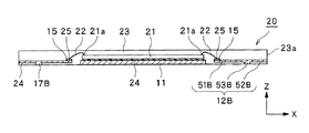
図5および図6に示すように、半導体装置(半導体パッケージ)20は、ダイパッド11と、ダイパッド11の周囲に配置された複数の第1リード部12A、複数の第2リード部12Bおよび複数の第3リード部12Cと、ダイパッド11上に搭載された半導体素子21と、リード部12A、12B、12Cと半導体素子21とを電気的に接続する複数のボンディングワイヤ(導電部材)22とを備えている。また、ダイパッド11、リード部12A、12B、12C、半導体素子21およびボンディングワイヤ22は、封止樹脂23によって樹脂封止されている。
As shown in FIGS. 5 and 6, the semiconductor device (semiconductor package) 20 includes a
このうち第1リード部12A、第2リード部12Bおよび第3リード部12Cは、封止樹脂23の周縁23aに沿ってこの順番に繰り返し配置されている。また、第1リード部12Aの第1端子部53Aは、第2リード部12Bの第2端子部53Bよりも外側(封止樹脂23の周縁23a側)に位置するとともに、その隣接する第2端子部53Bに対して封止樹脂23の周縁方向にずれて配置されている。さらに、第2リード部12Bの第2端子部53Bは、第3リード部12Cの第3端子部53Cよりも外側(封止樹脂23の周縁23a側)に位置するとともに、その隣接する第3端子部53Cに対して封止樹脂23の周縁方向にずれて配置されている。なお、封止樹脂23の周縁方向とは、封止樹脂23の周縁23aを構成する辺に沿う方向をいう。
Among these, the first lead portion 12 </ b> A, the second lead portion 12 </ b> B, and the third lead portion 12 </ b> C are repeatedly arranged in this order along the peripheral edge 23 a of the sealing
なお、ダイパッド11およびリード部12A、12B、12Cは、上述したリードフレーム10から作製されたものである。このダイパッド11およびリード部12A、12B、12Cの構成は、半導体装置20に含まれない領域を除き、上述した図1乃至図4に示すものと同様であるため、ここでは詳細な説明を省略する。
Note that the
また、半導体素子21としては、従来一般に用いられている各種半導体素子を使用することが可能であり、特に限定されないが、例えば集積回路、大規模集積回路、トランジスタ、サイリスタ、ダイオード等を用いることができる。この半導体素子21は、各々ボンディングワイヤ22が取り付けられる複数の電極21aを有している。また、半導体素子21は、例えばダイボンディングペースト又はめっき等の接着剤24により、ダイパッド11の表面に固定されている。
Further, as the
各ボンディングワイヤ22は、例えば金、銅等の導電性の良い材料からなっている。各ボンディングワイヤ22は、それぞれその一端が半導体素子21の電極21aに接続されるとともに、その他端が各リード部12A、12B、12Cの内部端子15にそれぞれ接続されている。なお、内部端子15には、ボンディングワイヤ22と密着性を向上させるめっき部25が設けられている。
Each
なお、半導体装置20の角部近傍に設けられた、内部領域51B、51Cを有していない第2リード部12Bおよび第3リード部12Cに関しては、それぞれ第2端子部53Bおよび第3端子部53Cの表面に、直接ボンディングワイヤ22が接続されている。当該第2端子部53Bおよび第3端子部53Cは、例えばグランド端子として用いられても良い。
In addition, regarding the
封止樹脂23としては、シリコーン樹脂やエポキシ樹脂等の熱硬化性樹脂、あるいはPPS樹脂等の熱可塑性樹脂を用いることができる。封止樹脂23全体の厚みは、300μm〜2700μm程度とすることができる。また、封止樹脂23の一辺(半導体装置20の一辺)は、例えば8mm〜16mmすることができる。なお、図5において、封止樹脂23のうち、ダイパッド11およびリード部12A、12B、12Cよりも表面側に位置する部分の表示を省略している。
As the sealing
リードフレームの製造方法
次に、図1乃至図4に示すリードフレーム10の製造方法について、図7(a)−(f)を用いて説明する。なお、図7(a)−(f)は、リードフレーム10の製造方法を示す断面図(図2に対応する図)である。
Manufacturing Method of Lead Frame Next, a manufacturing method of the
まず図7(a)に示すように、平板状の金属基板31を準備する。この金属基板31としては、銅、銅合金、42合金(Ni42%のFe合金)等の金属からなる基板を使用することができる。なお金属基板31は、その両面に対して脱脂等を行い、洗浄処理を施したものを使用することが好ましい。
First, as shown in FIG. 7A, a
次に、金属基板31の表裏全体にそれぞれ感光性レジスト32a、33aを塗布し、これを乾燥する(図7(b))。なお感光性レジスト32a、33aとしては、従来公知のものを使用することができる。
Next, photosensitive resists 32a and 33a are applied to the entire front and back surfaces of the
続いて、この金属基板31に対してフォトマスクを介して露光し、現像することにより、所望の開口部32b、33bを有するエッチング用レジスト層32、33を形成する(図7(c))。
Subsequently, the
次に、エッチング用レジスト層32、33を耐腐蝕膜として金属基板31に腐蝕液でエッチングを施す(図7(d))。これにより、ダイパッド11および複数のリード部12A、12B、12Cの外形(図1および図3参照)が形成される。なお、腐蝕液は、使用する金属基板31の材質に応じて適宜選択することができ、例えば、金属基板31として銅を用いる場合、通常、塩化第二鉄水溶液を使用し、金属基板31の両面からスプレーエッチングを行うことができる。
Next, the etching resist
その後、エッチング用レジスト層32、33を剥離して除去する(図7(e))。
Thereafter, the etching resist
なお、上記においては、金属基板31の両面側からスプレーエッチングを行う場合を例にとって説明したが、これに限られるものではない。例えば、金属基板31の片面ずつ2段階のスプレーエッチングを行っても良い。具体的には、まず所定のパターンをもつエッチング用レジスト層32、33を形成し(図7(c)参照)、その後、金属基板31の裏面側に耐エッチング性のある封止層を設け、この状態で金属基板31の表面側のみエッチングを実施する。次いで、当該裏面側の封止層を剥離し、金属基板31の表面側に封止層を設ける。このとき、表面側の封止層は、エッチング加工された金属基板31の表面側の凹部内にも進入する。続いて、金属基板31の露出した裏面のみをエッチングし、その後表面側の封止層を剥離することにより、ダイパッド11および複数のリード部12A、12B、12Cの外形が形成される。このように金属基板31の片面ずつスプレーエッチングを行うことにより、リード部12A、12B、12Cの変形を回避しやすいという効果が得られる。
In the above description, the case where spray etching is performed from both sides of the
次に、ボンディングワイヤ22と内部端子15との密着性を向上させるため、内部端子15にメッキ処理を施し、めっき部25を形成する(図7(f))。この場合、選択されるメッキ種は、ボンディングワイヤ22との密着性を確保できればその種類は問わないが、たとえばAgやAuなどの単層めっきでもよいし、Ni/PdやNi/Pd/Auがこの順に積層される複層めっきでもよい。また、めっき部25は、リード部12A、12B、12Cのうちボンディングワイヤ22との接続部のみに施してもよいし、リードフレーム10の全面に施してもよい。
Next, in order to improve the adhesion between the
このようにして、図1乃至図4に示すリードフレーム10が得られる。
In this way, the
半導体装置の製造方法
次に、図5および図6に示す半導体装置20の製造方法について、図8(a)−(e)を用いて説明する。
Manufacturing Method of Semiconductor Device Next, a manufacturing method of the
まず、例えば図7(a)−(f)に示す方法により、リードフレーム10を作製する(図8(a))。
First, for example, the
次に、リードフレーム10のダイパッド11上に、半導体素子21を搭載する。この場合、例えばダイボンディングペースト又はめっき等の接着剤24を用いて、半導体素子21をダイパッド11上に載置して固定する(ダイアタッチ工程)(図8(b))。
Next, the
次に、半導体素子21の各電極21aと、各リード部12A、12B、12Cのめっき部25(内部端子15)とを、それぞれボンディングワイヤ(導電部材)22によって互いに電気的に接続する(ワイヤボンディング工程)(図8(c))。
Next, each
次に、リードフレーム10に対して熱硬化性樹脂または熱可塑性樹脂を射出成形またはトランスファ成形することにより、封止樹脂23を形成する(図8(d))。このようにして、リードフレーム10、半導体素子21、リード部12A、12B、12Cおよびボンディングワイヤ22を封止する。
Next, the sealing
次に、各半導体素子21間の封止樹脂23をダイシングすることにより、リードフレーム10を各半導体装置20毎に分離する。この際、例えばダイヤモンド砥石からなるブレード(図示せず)を回転させながら、各半導体装置20間のリードフレーム10および封止樹脂23を切断しても良い。
Next, the
このようにして、図5および図6に示す半導体装置20が得られる(図8(e))。
In this way, the
以上説明したように、本実施の形態によれば、第1リード部12A、第2リード部12Bおよび第3リード部12Cは、支持リード13に沿ってこの順番に繰り返し配置されている。また、第1端子部53Aは、第2端子部53Bよりも外側に位置するとともに、その隣接する第2端子部53Bに対して支持リード13の長手方向にずれて配置されている。さらに、第2端子部53Bは、第3端子部53Cよりも外側に位置するとともに、その隣接する第3端子部53Cに対して支持リード13の長手方向にずれて配置されている。
このように、端子部53A、53B、53Cを3列に配置することにより、外部の実装基板(図示せず)に接続される外部端子17A、17B、17Cの数(ピン数)を増やすとともに、各外部端子17A、17B、17C間の距離を十分に確保することができる。
As described above, according to the present embodiment, the
Thus, by arranging the
変形例
次に、図9乃至図17により、本実施の形態によるリードフレームの変形例について説明する。図9乃至図17において、図1乃至図8に示す実施の形態と同一部分には同一の符号を付して、詳細な説明は省略する。
Modification Next, FIGS. 9 to 17, a description will be given of a variation of the lead frame according to the present embodiment. 9 to 17, the same parts as those of the embodiment shown in FIGS. 1 to 8 are denoted by the same reference numerals, and detailed description thereof is omitted.
変形例1
図9は、本実施の形態の変形例(変形例1)を示す部分拡大平面図(図4に対応する図)である。図9において、図1乃至図8に示す実施の形態と異なり、第2端子部53Bの平面形状を楕円形(小判形)としている。この場合、第2端子部53Bの外周のうち、内部領域51B側(ダイパッド11側)と外部領域52B側(支持リード13側)との両方に円弧形状部分が設けられている。また、第3端子部53Cの平面形状は、半円と長方形とを合わせた形状であり、円弧形状部分は、外部領域52C側(支持リード13側)に設けられている。これにより、隣接する端子部53A、53B、53C間の間隔(ピッチ)dを更に拡げることができるので、外部端子17A、17B、17C上の半田が他の外部端子17A、17B、17C上の半田と短絡する不具合(半田ブリッジ)をより確実に防止することができる。
FIG. 9 is a partially enlarged plan view (a diagram corresponding to FIG. 4) showing a modification (Modification 1) of the present embodiment. In FIG. 9, unlike the embodiment shown in FIGS. 1 to 8, the planar shape of the second
変形例2
図10は、本実施の形態の変形例(変形例2)を示す部分拡大平面図(図4に対応する図)である。図10において、第2端子部53Bだけでなく、第3端子部53Cの平面形状を楕円形(小判形)とした点が、図9(変形例1)と異なっている。すなわち、第3端子部53Cの外周のうち、内部領域51C側(ダイパッド11側)と外部領域52C側(支持リード13側)との両方に円弧形状部分が設けられている。これにより、図9(変形例1)おける効果に加え、半導体装置20を実装する際、外部端子17Cに付着した溶融半田が内部領域51C側(ダイパッド11側)に流れにくくする効果も得られる。
Modification 2
FIG. 10 is a partially enlarged plan view (a diagram corresponding to FIG. 4) showing a modification (modification 2) of the present embodiment. 10 differs from FIG. 9 (Modification 1) in that not only the second
変形例3
図11は、本実施の形態の変形例(変形例3)を示す部分拡大平面図(図3に対応する図)である。図11において、ダイパッド11の裏面外周に沿って薄肉部11aが形成されている点が、図1乃至図8に示す実施の形態と異なっている。この場合、薄肉部11aは、ダイパッド11および複数のリード部12A、12B、12Cの外形を形成する際(図7(e)参照)、ハーフエッチングによって形成される。このように、ダイパッド11の裏面外周に沿って薄肉部11aを設けたことにより、ダイパッド11と封止樹脂23との密着性を更に高めることができる。
FIG. 11 is a partially enlarged plan view (a diagram corresponding to FIG. 3) showing a modification (Modification 3) of the present embodiment. 11 is different from the embodiment shown in FIGS. 1 to 8 in that a
変形例4
図12は、本実施の形態の変形例(変形例4)を示す部分拡大平面図(図3に対応する図)である。図12において、ダイパッド11の表面外周に沿って、めっき部26が形成されている(図12の斜線部)。このように、ダイパッド11にめっき部26を形成したことにより、半導体素子21をダイパッド11に固定する際(図8(b))、ダイボンディングペースト又はめっき等の接着剤24がダイパッド11から流れ出る不具合を防止することができる。また、このめっき部26をグランド端子等の端子として用いることもできる。さらに、ダイパッド11の周囲に沿って複数の貫通口11bが形成されている。この貫通口11b内に封止樹脂23(後述)が進入することにより、ダイパッド11と封止樹脂23とを確実に密着させることができる。
FIG. 12 is a partially enlarged plan view (a diagram corresponding to FIG. 3) showing a modification (Modification 4) of the present embodiment. In FIG. 12, the
変形例5
図13は、本実施の形態の変形例(変形例5)を示す部分拡大平面図(図3に対応する図)である。図13において、支持リード13の長手方向各端部に設けられた第2リード部12Bおよび第3リード部12Cは、それぞれ内部領域51B、51Cを有している。これらリード部12B、12Cの内部領域51B、51Cは、各単位リードフレーム10aでそれぞれ吊りリード14に直接連結されている。この場合、リード部12B、12Cを例えばグランド端子として用いることができる。なお、支持リード13の長手方向端部に第1リード部12Aを設け、この第1リード部12Aを吊りリード14に連結しても良い。
FIG. 13 is a partially enlarged plan view (a diagram corresponding to FIG. 3) showing a modification (Modification 5) of the present embodiment. In FIG. 13, the
変形例6
図14は、本実施の形態の変形例(変形例6)を示す部分拡大平面図(図3に対応する図)である。図14において、ダイパッド11の表面に、ダイボンディングペースト又はめっき等の接着剤24の流れを止める流れ止め凹部11cが形成されている。流れ止め凹部11cは、ダイパッド11の一辺に沿って複数個配置されている。この流れ止め凹部11cは、ハーフエッチングにより表面側から薄肉化されることによって形成されたものである。なお、流れ止め凹部11cの平面形状は、例えばX字状(十字状)のほか、L字状、T字状、円形状、環形状又は多角形状としても良い。このように流れ止め凹部11cを設けたことにより、半導体素子21をダイパッド11に固定する際(図8(b))、接着剤24がダイパッド11から流れ出る不具合を防止することができる。
FIG. 14 is a partial enlarged plan view (a diagram corresponding to FIG. 3) showing a modification (Modification 6) of the present embodiment. In FIG. 14, a flow stop recess 11 c that stops the flow of an adhesive 24 such as a die bonding paste or plating is formed on the surface of the
変形例7
図15は、本実施の形態の変形例(変形例7)を示す部分拡大平面図(図3に対応する図)である。図15において、図1乃至図8に示す実施の形態と異なり、ダイパッド11と、リード部12A、12B、12Cとの間に、接続バー41が配置されている。この接続バー41は、X方向又はY方向に沿って一直線状に延びており、その長手方向両端部は、それぞれ吊りリード14に連結されている。また接続バー41には、複数の第4端子部18が所定間隔を空けて連結されている。各第4端子部18の表面には、ボンディングワイヤ22が接続される内部端子15が形成され、各第4端子部18の裏面には、外部の実装基板(図示せず)に接続される外部端子17Dが形成されている。この場合、各第4端子部18は、接続バー41に対して外側(支持リード13側)に突出しているが、これに限らず接続バー41に対して内側(ダイパッド11側)に突出していても良い。なお、半導体装置20の製造時に封止樹脂23によって樹脂封止された後(図8(d))、接続バー41の一部又は全部は、裏面側から例えばエッチング又はダイシングにより除去される。これにより、複数の第4端子部18がそれぞれ個別に分離される。このように端子部53A、53B、53C、18を4列に配置することにより、外部端子17A、17B、17C、17Dの数(ピン数)を更に増やすことができる。また、第4端子部18(外部端子17D)を接続バー41とは別途設けるのではなく、接続バー41の一部を除去した後、接続バー41の残部を第4端子部18として用いてもよい。
Modification 7
FIG. 15 is a partial enlarged plan view (a diagram corresponding to FIG. 3) showing a modification (Modification 7) of the present embodiment. In FIG. 15, unlike the embodiment shown in FIGS. 1 to 8, a
変形例8
図16(a)〜(c)は、本実施の形態の変形例(変形例8)を示す部分拡大底面図である。このうち図16(a)は、第1端子部53Aの裏面(外部端子17A)の周囲を示す図であり、図16(b)は、第2端子部53Bの裏面(外部端子17B)の周囲を示す図であり、図16(c)は、第3端子部53Cの裏面(外部端子17C)の周囲を示す図である。図16(a)〜(c)中、網掛けされた領域は、裏面側からハーフエッチングにより薄肉化されている領域を示している。
Modification 8
FIGS. 16A to 16C are partially enlarged bottom views showing a modified example (modified example 8) of the present embodiment. 16A is a view showing the periphery of the back surface (external terminal 17A) of the first
図16(a)において、第1端子部53Aの側方(第1リード部12Aの長さ方向に垂直な方向)の位置PC1、PB1における、第3リード部12Cの外部領域52C又は第2リード部12Bの外部領域52Bの厚みをt1とする。また、図16(b)において、第2端子部53Bの側方(第2リード部12Bの長さ方向に垂直な方向)の位置PA1、PC2における、第1リード部12Aの内部領域51A又は第3リード部12Cの外部領域52Cの厚みをt2とする。さらに、図16(c)において、第3端子部53Cの側方(第3リード部12Cの長さ方向に垂直な方向)の位置PB2、PA2における、第2リード部12Bの内部領域51B又は第1リード部12Aの内部領域51Aの厚みをt3とする。このとき、t1>t2>t3という関係が成り立つ。
In FIG. 16A, the
また、図16(a)において、第1リード部12Aの第1端子部53Aに隣接する位置PA3(第1リード部12Aの長さ方向に隣接する位置)における、内部領域51Aの厚みをt4とする。また、図16(b)において、第2リード部12Bの第2端子部53Bに隣接する位置PB3、PB4(第2リード部12Bの長さ方向に隣接する位置)における、内部領域51B又は外部領域52Bの厚みをt5とする。さらに、図16(c)において、第3リード部12Cの第3端子部53Cに隣接する位置PC3、PC4(第3リード部12Cの長さ方向に隣接する位置)における、内部領域51C又は外部領域52Cの厚みをt6とする。このとき、t4>t5>t6という関係が成り立つ。
In FIG. 16A, the thickness of the
このように、各リード部12A、12B、12Cは、根元側(支持リード13側)から先端側(ダイパッド11側)へ向けて徐々に厚みが薄くなっている。これにより、リード部12A、12B、12Cの根元側(支持リード13側)の強度を高め、リード部12A、12B、12Cの変形を防止することができる。
In this way, the thickness of each
図16(a)に示すように、順に並んで配置されたリード部12A、12C、12Bにおいて、第1リード部12Aの第1端子部53Aと第2リード部12Bの第2端子部53Bとの間に位置する第3リード部12Cの外部領域52Cに、外部領域52Cの他の部分よりも幅が広い幅広部52wが形成されている。また、図16(b)に示すように、順に並んで配置されたリード部12B、12A、12Cにおいて、第2リード部12Bの第2端子部53Bと第3リード部12Cの第3端子部53Cとの間に位置する第1リード部12Aの内部領域51Aに、内部領域51Aの他の部分よりも幅が広い幅広部51wが形成されている。このように、内部領域51A、外部領域52Cにそれぞれ幅広部51w、52wを設けたことにより、リード部12A、12Cの強度を高め、リード部12A、12Cの変形を防止することができる。
As shown in FIG. 16A, in the
図16(a)に示すように、支持リード13と単位リードフレーム10aの外周部との間に、補強領域13a(二点鎖線)が設けられている。補強領域13aは、支持リード13から内側(ダイパッド11側)に延出するとともに、第2リード部12Bと第3リード部12Cとの間に延びて第2リード部12Bと第3リード部12Cとを連結している。この場合、補強領域13aは、裏面側からハーフエッチングにより薄肉に形成されているが、これに限らず、薄肉化されることなく支持リード13と同一の厚みを有していても良い。このように、補強領域13aを設けたことにより、リード部12B、12Cの根元の強度を高め、リード部12B、12Cの変形を防止することができる。
As shown in FIG. 16A, a reinforcing region 13a (two-dot chain line) is provided between the
図16(b)に示すように、第2端子部53Bの外部端子17Bは、先端側(ダイパッド11側)に位置する先端側周縁部53sと、根元側(支持リード13側)に位置する根元側周縁部53tとを有している。先端側周縁部53sおよび根元側周縁部53tは、それぞれ円弧状部分を有しており、先端側周縁部53sの円弧状部分の曲率半径は、根元側周縁部53tの円弧状部分の曲率半径よりも小さくなっている。これにより、半導体装置20を外部の実装基板(図示せず)に実装する際に用いる導電性接合部、例えば半田ペーストの流れ方向を制御することが可能となり、外部端子17A、17B、17C間の短絡を防ぐことができる。具体的には、先端側周縁部53sの円弧状部分の曲率半径は、例えば30μm〜70μmであり、根元側周縁部53tの円弧状部分の曲率半径は、例えば100μm〜250μmである。なお、第3端子部53Cの外部端子17Cの形状についても同様である(図16(c)参照)。
As shown in FIG. 16B, the
図17は、図16(a)のXVII−XVII線断面図である。図17に示すように、第1リード部12Aの第1端子部53Aは、その両側面が内方に向けて湾曲した形状を有している。外部端子17Aの幅wA2は、第1端子部53Aの表面の幅wA1よりも広くなっている。これにより、互いに隣接する第1リード部12Aと、第2リード部12B又は第3リード部12Cとの間隔を狭めた場合であっても、外部端子17Aの面積を広く確保することができ、外部端子17Aと外部の実装基板(図示せず)とを確実に接続することができる。なお、第2リード部12Bの第2端子部53Bおよび第3リード部12Cの第3端子部53Cについても、同様に、その両側面が内方に向けて湾曲した形状を有しており、かつ外部端子17B、17Cの幅が第2端子部53B、第3端子部53Cの表面の幅よりも広くなっている。
FIG. 17 is a sectional view taken along line XVII-XVII in FIG. As shown in FIG. 17, the first
上記実施の形態および変形例に開示されている複数の構成要素を必要に応じて適宜組合せることも可能である。あるいは、上記実施の形態および変形例に示される全構成要素から幾つかの構成要素を削除してもよい。 It is also possible to appropriately combine a plurality of constituent elements disclosed in the embodiment and the modification examples as necessary. Or you may delete a some component from all the components shown by the said embodiment and modification.
10 リードフレーム
10a 単位リードフレーム
11 ダイパッド
12A 第1リード部
12B 第2リード部
12C 第3リード部
13 支持リード(支持部材)
14 吊りリード
15 内部端子
17A、17B、17C 外部端子
20 半導体装置
21 半導体素子
22 ボンディングワイヤ(導電部材)
23 封止樹脂
24 接着剤
25 めっき部
51A、51B、51C 内部領域
52B、52C 外部領域
53A 第1端子部
53B 第2端子部
53C 第3端子部
DESCRIPTION OF
14
23
Claims (12)
半導体素子が搭載されるダイパッドと、
前記ダイパッド周囲に設けられ、それぞれ第1端子部を含む複数の第1リード部と、
前記ダイパッド周囲に設けられ、それぞれ第2端子部を含む複数の第2リード部と、
前記ダイパッド周囲に設けられ、それぞれ第3端子部を含む複数の第3リード部とを備え、
前記第1リード部、前記第2リード部および前記第3リード部は、それぞれ支持リードに支持され、
前記第1リード部の前記第1端子部は、前記第2リード部の前記第2端子部よりも外側に位置するとともに、当該第1リード部に隣接する第2リード部の前記第2端子部に対して前記支持リードの長手方向にずれて配置され、
前記第2リード部の前記第2端子部は、前記第3リード部の前記第3端子部よりも外側に位置するとともに、当該第2リード部に隣接する第3リード部の前記第3端子部に対して前記支持リードの長手方向にずれて配置され、
前記第1リード部、前記第2リード部および前記第3リード部は、前記支持リードに沿ってこの順番に繰り返し配置され、
前記第1リード部、前記第2リード部および前記第3リード部は、それぞれ前記第1端子部、前記第2端子部および前記第3端子部から前記ダイパッド側に延びる内部領域を有し、
前記第2リード部および前記第3リード部は、それぞれ前記第2端子部および前記第3端子部から前記支持リード側に延びる外部領域を有し、
前記第1リード部および前記第3リード部は、それぞれ平面から見て前記支持リードに対して垂直な方向に延びる垂直領域と、前記支持リードに対して傾斜して延びる傾斜領域とを有し、
前記第2リード部は、平面から見て前記支持リードに対して垂直な方向に延びる垂直領域を有し、
前記第1リード部、前記第2リード部および前記第3リード部の前記内部領域のうち、前記第1端子部、前記第2端子部または前記第3端子部との連結部分は、それぞれ前記垂直領域となっており、
前記第2リード部および前記第3リード部の前記外部領域のうち、少なくとも前記第2端子部または前記第3端子部との連結部分は、それぞれ前記垂直領域となっており、
前記第1リード部の前記内部領域が、前記支持リードに対して垂直な方向において、前記第2端子部と前記第3端子部との間に前記傾斜領域を有し、
前記第3リード部の前記外部領域が、前記支持リードに対して垂直な方向において、前記第1端子部と前記第2端子部との間に前記傾斜領域を有することを特徴とするリードフレーム。 A lead frame for a semiconductor device,
A die pad on which a semiconductor element is mounted;
A plurality of first lead portions provided around the die pad, each including a first terminal portion;
A plurality of second lead portions provided around the die pad, each including a second terminal portion;
A plurality of third lead portions provided around the die pad and each including a third terminal portion;
The first lead portion, the second lead portion, and the third lead portion are each supported by a support lead,
The first terminal portion of the first lead portion is located outside the second terminal portion of the second lead portion, and the second terminal portion of the second lead portion adjacent to the first lead portion. With respect to the longitudinal direction of the support lead,
The second terminal portion of the second lead portion is located outside the third terminal portion of the third lead portion, and the third terminal portion of the third lead portion adjacent to the second lead portion. With respect to the longitudinal direction of the support lead ,
The first lead portion, the second lead portion, and the third lead portion are repeatedly arranged in this order along the support lead,
The first lead portion, the second lead portion, and the third lead portion have internal regions extending from the first terminal portion, the second terminal portion, and the third terminal portion to the die pad side, respectively.
The second lead portion and the third lead portion have external regions extending from the second terminal portion and the third terminal portion to the support lead side, respectively.
The first lead portion and the third lead portion each have a vertical region extending in a direction perpendicular to the support lead when viewed from the plane, and an inclined region extending inclined with respect to the support lead,
The second lead portion has a vertical region extending in a direction perpendicular to the support lead when viewed from a plane,
Of the internal regions of the first lead portion, the second lead portion, and the third lead portion, the connecting portions with the first terminal portion, the second terminal portion, or the third terminal portion are each vertical. Is an area,
Of the external regions of the second lead portion and the third lead portion, at least the connection portion with the second terminal portion or the third terminal portion is the vertical region, respectively.
The inner region of the first lead portion has the inclined region between the second terminal portion and the third terminal portion in a direction perpendicular to the support lead;
The lead frame, wherein the external region of the third lead portion has the inclined region between the first terminal portion and the second terminal portion in a direction perpendicular to the support lead .
ダイパッドと、
前記ダイパッド周囲に設けられ、それぞれ第1端子部を含む複数の第1リード部と、
前記ダイパッド周囲に設けられ、それぞれ第2端子部を含む複数の第2リード部と、
前記ダイパッド周囲に設けられ、それぞれ第3端子部を含む複数の第3リード部と、
前記ダイパッド上に搭載された半導体素子と、
前記半導体素子と、前記第1リード部、前記第2リード部および前記第3リード部とをそれぞれ電気的に接続する導電部材と、
前記ダイパッドと、前記第1リード部と、前記第2リード部と、前記第3リード部と、前記半導体素子と、前記導電部材とを封止する封止樹脂とを備え、
前記第1リード部の前記第1端子部は、前記第2リード部の前記第2端子部よりも外側に位置するとともに、当該第1リード部に隣接する第2リード部の前記第2端子部に対して前記封止樹脂の周縁方向にずれて配置され、
前記第2リード部の前記第2端子部は、前記第3リード部の前記第3端子部よりも外側に位置するとともに、当該第2リード部に隣接する第3リード部の前記第3端子部に対して前記封止樹脂の周縁方向にずれて配置され、
前記第1リード部、前記第2リード部および前記第3リード部は、前記封止樹脂の周縁に沿ってこの順番に繰り返し配置され、
前記第1リード部、前記第2リード部および前記第3リード部は、それぞれ前記第1端子部、前記第2端子部および前記第3端子部から前記ダイパッド側に延びる内部領域を有し、
前記第2リード部および前記第3リード部は、それぞれ前記第2端子部および前記第3端子部から前記封止樹脂の周縁側に延びる外部領域を有し、
前記第1リード部および前記第3リード部は、それぞれ平面から見て前記封止樹脂の周縁に対して垂直な方向に延びる垂直領域と、前記封止樹脂の周縁に対して傾斜して延びる傾斜領域とを有し、
前記第2リード部は、平面から見て前記封止樹脂の周縁に対して垂直な方向に延びる垂直領域を有し、
前記第1リード部、前記第2リード部および前記第3リード部の前記内部領域のうち、前記第1端子部、前記第2端子部または前記第3端子部との連結部分は、それぞれ前記垂直領域となっており、
前記第2リード部および前記第3リード部の前記外部領域のうち、少なくとも前記第2端子部または前記第3端子部との連結部分は、それぞれ前記垂直領域となっており、
前記第1リード部の前記内部領域が、前記封止樹脂の周縁に対して垂直な方向において、前記第2端子部と前記第3端子部との間に前記傾斜領域を有し、
前記第3リード部の前記外部領域が、前記封止樹脂の周縁に対して垂直な方向において、前記第1端子部と前記第2端子部との間に前記傾斜領域を有することを特徴とする半導体装置。 A semiconductor device,
Die pad,
A plurality of first lead portions provided around the die pad, each including a first terminal portion;
A plurality of second lead portions provided around the die pad, each including a second terminal portion;
A plurality of third lead portions provided around the die pad, each including a third terminal portion;
A semiconductor element mounted on the die pad;
A conductive member that electrically connects the semiconductor element to the first lead portion, the second lead portion, and the third lead portion;
A sealing resin that seals the die pad, the first lead portion, the second lead portion, the third lead portion, the semiconductor element, and the conductive member;
The first terminal portion of the first lead portion is located outside the second terminal portion of the second lead portion, and the second terminal portion of the second lead portion adjacent to the first lead portion. Are displaced in the peripheral direction of the sealing resin,
The second terminal portion of the second lead portion is located outside the third terminal portion of the third lead portion, and the third terminal portion of the third lead portion adjacent to the second lead portion. Are displaced in the peripheral direction of the sealing resin ,
The first lead portion, the second lead portion, and the third lead portion are repeatedly arranged in this order along the periphery of the sealing resin,
The first lead portion, the second lead portion, and the third lead portion have internal regions extending from the first terminal portion, the second terminal portion, and the third terminal portion to the die pad side, respectively.
The second lead portion and the third lead portion have external regions extending from the second terminal portion and the third terminal portion to the peripheral side of the sealing resin, respectively.
The first lead portion and the third lead portion each have a vertical region extending in a direction perpendicular to the peripheral edge of the sealing resin as viewed from above, and an inclination extending obliquely with respect to the peripheral edge of the sealing resin And having an area
The second lead portion has a vertical region extending in a direction perpendicular to the periphery of the sealing resin when viewed from a plane,
Of the internal regions of the first lead portion, the second lead portion, and the third lead portion, each of the connecting portions with the first terminal portion, the second terminal portion, or the third terminal portion is the vertical portion. Is an area,
Of the external regions of the second lead portion and the third lead portion, at least the connection portion with the second terminal portion or the third terminal portion is the vertical region, respectively.
The inner region of the first lead portion has the inclined region between the second terminal portion and the third terminal portion in a direction perpendicular to the periphery of the sealing resin;
The external region of the third lead portion has the inclined region between the first terminal portion and the second terminal portion in a direction perpendicular to the periphery of the sealing resin. Semiconductor device.
金属基板を準備する工程と、
前記金属基板をエッチング加工することにより、前記金属基板に前記ダイパッド、前記複数の第1リード部、前記複数の第2リード部および前記複数の第3リード部を形成する工程とを備えたことを特徴とするリードフレームの製造方法。 A lead frame manufacturing method according to any one of claims 1 to 9 ,
Preparing a metal substrate;
Forming the die pad, the plurality of first lead portions, the plurality of second lead portions, and the plurality of third lead portions on the metal substrate by etching the metal substrate. A method for manufacturing a lead frame.
請求項1乃至9のいずれか一項記載のリードフレームを準備する工程と、
前記リードフレームの前記ダイパッド上に前記半導体素子を搭載する工程と、
前記半導体素子と、前記第1リード部、前記第2リード部および前記第3リード部とを導電部材により電気的に接続する工程と、
前記ダイパッドと、前記複数の第1リード部と、前記複数の第2リード部と、前記複数の第3リード部と、前記半導体素子と、前記導電部材とを封止樹脂により封止する工程とを備えたことを特徴とする半導体装置の製造方法。 A method for manufacturing a semiconductor device, comprising:
Preparing a lead frame according to any one of claims 1 to 9 ,
Mounting the semiconductor element on the die pad of the lead frame;
Electrically connecting the semiconductor element and the first lead portion, the second lead portion, and the third lead portion by a conductive member;
Sealing the die pad, the plurality of first lead portions, the plurality of second lead portions, the plurality of third lead portions, the semiconductor element, and the conductive member with a sealing resin; A method for manufacturing a semiconductor device, comprising:
Priority Applications (1)
| Application Number | Priority Date | Filing Date | Title |
|---|---|---|---|
| JP2015166792A JP6607441B2 (en) | 2014-08-27 | 2015-08-26 | Lead frame and manufacturing method thereof, and semiconductor device and manufacturing method thereof |
Applications Claiming Priority (3)
| Application Number | Priority Date | Filing Date | Title |
|---|---|---|---|
| JP2014172833 | 2014-08-27 | ||
| JP2014172833 | 2014-08-27 | ||
| JP2015166792A JP6607441B2 (en) | 2014-08-27 | 2015-08-26 | Lead frame and manufacturing method thereof, and semiconductor device and manufacturing method thereof |
Publications (2)
| Publication Number | Publication Date |
|---|---|
| JP2016048784A JP2016048784A (en) | 2016-04-07 |
| JP6607441B2 true JP6607441B2 (en) | 2019-11-20 |
Family
ID=55649511
Family Applications (1)
| Application Number | Title | Priority Date | Filing Date |
|---|---|---|---|
| JP2015166792A Active JP6607441B2 (en) | 2014-08-27 | 2015-08-26 | Lead frame and manufacturing method thereof, and semiconductor device and manufacturing method thereof |
Country Status (1)
| Country | Link |
|---|---|
| JP (1) | JP6607441B2 (en) |
Families Citing this family (3)
| Publication number | Priority date | Publication date | Assignee | Title |
|---|---|---|---|---|
| JP7073637B2 (en) * | 2017-06-16 | 2022-05-24 | 大日本印刷株式会社 | Lead frames and semiconductor devices |
| JP7215110B2 (en) * | 2018-11-27 | 2023-01-31 | 大日本印刷株式会社 | Lead frames and semiconductor equipment |
| JP7468056B2 (en) | 2020-03-26 | 2024-04-16 | 大日本印刷株式会社 | Lead frame and manufacturing method thereof, and semiconductor device and manufacturing method thereof |
Family Cites Families (9)
| Publication number | Priority date | Publication date | Assignee | Title |
|---|---|---|---|---|
| JPH09246447A (en) * | 1996-03-12 | 1997-09-19 | Hitachi Ltd | Semiconductor device and manufacture thereof |
| JP3292082B2 (en) * | 1997-03-10 | 2002-06-17 | 松下電器産業株式会社 | Terminal land frame and method of manufacturing resin-encapsulated semiconductor device using the same |
| JP3003653B2 (en) * | 1997-11-27 | 2000-01-31 | 日本電気株式会社 | Ball grid array type semiconductor device |
| JP2004214233A (en) * | 2002-12-26 | 2004-07-29 | Renesas Technology Corp | Semiconductor device and manufacturing method therefor |
| JP4533875B2 (en) * | 2006-09-12 | 2010-09-01 | 株式会社三井ハイテック | Semiconductor device, lead frame product used in the semiconductor device, and method for manufacturing the semiconductor device |
| JP4531073B2 (en) * | 2007-03-20 | 2010-08-25 | 三洋電機株式会社 | Semiconductor device |
| JP2010010634A (en) * | 2008-06-30 | 2010-01-14 | Shinko Electric Ind Co Ltd | Lead frame, and method of manufacturing semiconductor device |
| US20110140253A1 (en) * | 2009-12-14 | 2011-06-16 | National Semiconductor Corporation | Dap ground bond enhancement |
| JP2013069741A (en) * | 2011-09-21 | 2013-04-18 | Renesas Electronics Corp | Lead frame, semiconductor device, method for manufacturing lead frame and method for manufacturing semiconductor device |
-
2015
- 2015-08-26 JP JP2015166792A patent/JP6607441B2/en active Active
Also Published As
| Publication number | Publication date |
|---|---|
| JP2016048784A (en) | 2016-04-07 |
Similar Documents
| Publication | Publication Date | Title |
|---|---|---|
| JP4091050B2 (en) | Manufacturing method of semiconductor device | |
| JP6205816B2 (en) | Lead frame and manufacturing method thereof, and semiconductor device and manufacturing method thereof | |
| JP6319644B2 (en) | Lead frame, manufacturing method thereof, and manufacturing method of semiconductor device | |
| JP6607441B2 (en) | Lead frame and manufacturing method thereof, and semiconductor device and manufacturing method thereof | |
| JP7174363B2 (en) | Lead frames and semiconductor equipment | |
| CN110943064A (en) | Lead frame and method of manufacturing the same | |
| JP2018022772A (en) | Lead frame | |
| JP6379448B2 (en) | Lead frame and manufacturing method thereof, and semiconductor device and manufacturing method thereof | |
| JP6946870B2 (en) | Lead frames, semiconductor devices, and methods for manufacturing semiconductor devices | |
| JP6465394B2 (en) | Lead frame and manufacturing method thereof, and semiconductor device and manufacturing method thereof | |
| JP6807050B2 (en) | Lead frames and semiconductor devices | |
| JP7380750B2 (en) | Lead frames and semiconductor devices | |
| JP6436202B2 (en) | Lead frame and manufacturing method thereof, and semiconductor device and manufacturing method thereof | |
| JP2015060876A (en) | Method of manufacturing semiconductor device | |
| JP2018137315A (en) | Lead frame and semiconductor device | |
| JP7064721B2 (en) | Lead frames and semiconductor devices | |
| JP7061278B2 (en) | Lead frames and semiconductor devices | |
| JP2018093093A (en) | Lead frame and semiconductor device | |
| JP2009231322A (en) | Manufacturing method of semiconductor device | |
| JP2015154042A (en) | Lead frame and manufacturing method therefor, and semiconductor device and manufacturing method therefor | |
| JP6807043B2 (en) | Lead frames and semiconductor devices | |
| JP6967190B2 (en) | Lead frame | |
| JP2018088461A (en) | Wiring board and semiconductor device | |
| JP6788825B2 (en) | Lead frames and semiconductor devices | |
| JP6428013B2 (en) | Lead frame member and manufacturing method thereof, and semiconductor device and manufacturing method thereof |
Legal Events
| Date | Code | Title | Description |
|---|---|---|---|
| A621 | Written request for application examination |
Free format text: JAPANESE INTERMEDIATE CODE: A621 Effective date: 20180625 |
|
| A977 | Report on retrieval |
Free format text: JAPANESE INTERMEDIATE CODE: A971007 Effective date: 20190221 |
|
| A131 | Notification of reasons for refusal |
Free format text: JAPANESE INTERMEDIATE CODE: A131 Effective date: 20190226 |
|
| A521 | Written amendment |
Free format text: JAPANESE INTERMEDIATE CODE: A523 Effective date: 20190426 |
|
| TRDD | Decision of grant or rejection written | ||
| A01 | Written decision to grant a patent or to grant a registration (utility model) |
Free format text: JAPANESE INTERMEDIATE CODE: A01 Effective date: 20190927 |
|
| A61 | First payment of annual fees (during grant procedure) |
Free format text: JAPANESE INTERMEDIATE CODE: A61 Effective date: 20191010 |
|
| R150 | Certificate of patent or registration of utility model |
Ref document number: 6607441 Country of ref document: JP Free format text: JAPANESE INTERMEDIATE CODE: R150 |