JP6584149B2 - 撮像装置 - Google Patents
撮像装置 Download PDFInfo
- Publication number
- JP6584149B2 JP6584149B2 JP2015109420A JP2015109420A JP6584149B2 JP 6584149 B2 JP6584149 B2 JP 6584149B2 JP 2015109420 A JP2015109420 A JP 2015109420A JP 2015109420 A JP2015109420 A JP 2015109420A JP 6584149 B2 JP6584149 B2 JP 6584149B2
- Authority
- JP
- Japan
- Prior art keywords
- image sensor
- image
- pupil
- photoelectric conversion
- pair
- Prior art date
- Legal status (The legal status is an assumption and is not a legal conclusion. Google has not performed a legal analysis and makes no representation as to the accuracy of the status listed.)
- Expired - Fee Related
Links
- 238000003384 imaging method Methods 0.000 title claims description 151
- 210000001747 pupil Anatomy 0.000 claims description 297
- 238000006243 chemical reaction Methods 0.000 claims description 161
- 238000001514 detection method Methods 0.000 claims description 149
- 230000004907 flux Effects 0.000 claims description 14
- 230000003287 optical effect Effects 0.000 description 52
- 238000010586 diagram Methods 0.000 description 30
- 238000000034 method Methods 0.000 description 28
- 230000008569 process Effects 0.000 description 25
- 230000007423 decrease Effects 0.000 description 17
- 239000010410 layer Substances 0.000 description 16
- 238000004891 communication Methods 0.000 description 15
- 230000005484 gravity Effects 0.000 description 15
- 238000012545 processing Methods 0.000 description 12
- 101100395484 Arabidopsis thaliana HPD gene Proteins 0.000 description 8
- 101100463166 Oryza sativa subsp. japonica PDS gene Proteins 0.000 description 8
- 101150061817 PDS1 gene Proteins 0.000 description 8
- 230000006870 function Effects 0.000 description 7
- 239000011229 interlayer Substances 0.000 description 7
- 101000726148 Homo sapiens Protein crumbs homolog 1 Proteins 0.000 description 6
- 102100027331 Protein crumbs homolog 1 Human genes 0.000 description 6
- 101000825534 Saccharomyces cerevisiae (strain ATCC 204508 / S288c) 40S ribosomal protein S2 Proteins 0.000 description 6
- XUIMIQQOPSSXEZ-UHFFFAOYSA-N Silicon Chemical compound [Si] XUIMIQQOPSSXEZ-UHFFFAOYSA-N 0.000 description 6
- ORQBXQOJMQIAOY-UHFFFAOYSA-N nobelium Chemical compound [No] ORQBXQOJMQIAOY-UHFFFAOYSA-N 0.000 description 6
- 229910052710 silicon Inorganic materials 0.000 description 6
- 239000010703 silicon Substances 0.000 description 6
- 239000000758 substrate Substances 0.000 description 6
- 238000009825 accumulation Methods 0.000 description 5
- 238000000926 separation method Methods 0.000 description 5
- 230000008859 change Effects 0.000 description 4
- 239000011295 pitch Substances 0.000 description 4
- 238000001454 recorded image Methods 0.000 description 4
- 239000007787 solid Substances 0.000 description 4
- 238000004422 calculation algorithm Methods 0.000 description 3
- 230000000694 effects Effects 0.000 description 3
- 230000016507 interphase Effects 0.000 description 3
- 239000004973 liquid crystal related substance Substances 0.000 description 3
- 238000005259 measurement Methods 0.000 description 3
- 230000035945 sensitivity Effects 0.000 description 3
- VYPSYNLAJGMNEJ-UHFFFAOYSA-N silicon dioxide Inorganic materials O=[Si]=O VYPSYNLAJGMNEJ-UHFFFAOYSA-N 0.000 description 3
- 238000012546 transfer Methods 0.000 description 3
- 101001105683 Homo sapiens Pre-mRNA-processing-splicing factor 8 Proteins 0.000 description 2
- 102100021231 Pre-mRNA-processing-splicing factor 8 Human genes 0.000 description 2
- 101000862778 Saccharomyces cerevisiae (strain ATCC 204508 / S288c) 40S ribosomal protein S3 Proteins 0.000 description 2
- 230000009471 action Effects 0.000 description 2
- 230000015556 catabolic process Effects 0.000 description 2
- 238000012937 correction Methods 0.000 description 2
- 238000006731 degradation reaction Methods 0.000 description 2
- 230000006866 deterioration Effects 0.000 description 2
- 101150002378 gC gene Proteins 0.000 description 2
- 230000014509 gene expression Effects 0.000 description 2
- 230000004048 modification Effects 0.000 description 2
- 238000012986 modification Methods 0.000 description 2
- 101001080808 Homo sapiens PH and SEC7 domain-containing protein 2 Proteins 0.000 description 1
- 102100027455 PH and SEC7 domain-containing protein 2 Human genes 0.000 description 1
- 101100212791 Saccharomyces cerevisiae (strain ATCC 204508 / S288c) YBL068W-A gene Proteins 0.000 description 1
- 229910052581 Si3N4 Inorganic materials 0.000 description 1
- 230000005540 biological transmission Effects 0.000 description 1
- 238000004364 calculation method Methods 0.000 description 1
- 230000006835 compression Effects 0.000 description 1
- 238000007906 compression Methods 0.000 description 1
- 238000006073 displacement reaction Methods 0.000 description 1
- 230000007274 generation of a signal involved in cell-cell signaling Effects 0.000 description 1
- 230000006872 improvement Effects 0.000 description 1
- 230000010354 integration Effects 0.000 description 1
- 239000011159 matrix material Substances 0.000 description 1
- 238000004091 panning Methods 0.000 description 1
- 230000002093 peripheral effect Effects 0.000 description 1
- 238000005498 polishing Methods 0.000 description 1
- 230000009467 reduction Effects 0.000 description 1
- 230000004044 response Effects 0.000 description 1
- 235000012239 silicon dioxide Nutrition 0.000 description 1
- 239000000377 silicon dioxide Substances 0.000 description 1
- HQVNEWCFYHHQES-UHFFFAOYSA-N silicon nitride Chemical compound N12[Si]34N5[Si]62N3[Si]51N64 HQVNEWCFYHHQES-UHFFFAOYSA-N 0.000 description 1
- 239000000126 substance Substances 0.000 description 1
- 238000002834 transmittance Methods 0.000 description 1
Images


Classifications
-
- H—ELECTRICITY
- H04—ELECTRIC COMMUNICATION TECHNIQUE
- H04N—PICTORIAL COMMUNICATION, e.g. TELEVISION
- H04N23/00—Cameras or camera modules comprising electronic image sensors; Control thereof
- H04N23/45—Cameras or camera modules comprising electronic image sensors; Control thereof for generating image signals from two or more image sensors being of different type or operating in different modes, e.g. with a CMOS sensor for moving images in combination with a charge-coupled device [CCD] for still images
-
- G—PHYSICS
- G03—PHOTOGRAPHY; CINEMATOGRAPHY; ANALOGOUS TECHNIQUES USING WAVES OTHER THAN OPTICAL WAVES; ELECTROGRAPHY; HOLOGRAPHY
- G03B—APPARATUS OR ARRANGEMENTS FOR TAKING PHOTOGRAPHS OR FOR PROJECTING OR VIEWING THEM; APPARATUS OR ARRANGEMENTS EMPLOYING ANALOGOUS TECHNIQUES USING WAVES OTHER THAN OPTICAL WAVES; ACCESSORIES THEREFOR
- G03B13/00—Viewfinders; Focusing aids for cameras; Means for focusing for cameras; Autofocus systems for cameras
- G03B13/32—Means for focusing
- G03B13/34—Power focusing
- G03B13/36—Autofocus systems
-
- H—ELECTRICITY
- H01—ELECTRIC ELEMENTS
- H01L—SEMICONDUCTOR DEVICES NOT COVERED BY CLASS H10
- H01L27/00—Devices consisting of a plurality of semiconductor or other solid-state components formed in or on a common substrate
- H01L27/14—Devices consisting of a plurality of semiconductor or other solid-state components formed in or on a common substrate including semiconductor components sensitive to infrared radiation, light, electromagnetic radiation of shorter wavelength or corpuscular radiation and specially adapted either for the conversion of the energy of such radiation into electrical energy or for the control of electrical energy by such radiation
- H01L27/144—Devices controlled by radiation
- H01L27/146—Imager structures
- H01L27/14601—Structural or functional details thereof
- H01L27/14625—Optical elements or arrangements associated with the device
- H01L27/14627—Microlenses
-
- H—ELECTRICITY
- H01—ELECTRIC ELEMENTS
- H01L—SEMICONDUCTOR DEVICES NOT COVERED BY CLASS H10
- H01L27/00—Devices consisting of a plurality of semiconductor or other solid-state components formed in or on a common substrate
- H01L27/14—Devices consisting of a plurality of semiconductor or other solid-state components formed in or on a common substrate including semiconductor components sensitive to infrared radiation, light, electromagnetic radiation of shorter wavelength or corpuscular radiation and specially adapted either for the conversion of the energy of such radiation into electrical energy or for the control of electrical energy by such radiation
- H01L27/144—Devices controlled by radiation
- H01L27/146—Imager structures
- H01L27/14601—Structural or functional details thereof
- H01L27/14625—Optical elements or arrangements associated with the device
- H01L27/14629—Reflectors
-
- H—ELECTRICITY
- H04—ELECTRIC COMMUNICATION TECHNIQUE
- H04N—PICTORIAL COMMUNICATION, e.g. TELEVISION
- H04N23/00—Cameras or camera modules comprising electronic image sensors; Control thereof
- H04N23/60—Control of cameras or camera modules
- H04N23/667—Camera operation mode switching, e.g. between still and video, sport and normal or high- and low-resolution modes
-
- H—ELECTRICITY
- H04—ELECTRIC COMMUNICATION TECHNIQUE
- H04N—PICTORIAL COMMUNICATION, e.g. TELEVISION
- H04N23/00—Cameras or camera modules comprising electronic image sensors; Control thereof
- H04N23/60—Control of cameras or camera modules
- H04N23/67—Focus control based on electronic image sensor signals
- H04N23/672—Focus control based on electronic image sensor signals based on the phase difference signals
-
- H—ELECTRICITY
- H04—ELECTRIC COMMUNICATION TECHNIQUE
- H04N—PICTORIAL COMMUNICATION, e.g. TELEVISION
- H04N25/00—Circuitry of solid-state image sensors [SSIS]; Control thereof
- H04N25/70—SSIS architectures; Circuits associated therewith
- H04N25/703—SSIS architectures incorporating pixels for producing signals other than image signals
- H04N25/704—Pixels specially adapted for focusing, e.g. phase difference pixel sets
-
- H—ELECTRICITY
- H04—ELECTRIC COMMUNICATION TECHNIQUE
- H04N—PICTORIAL COMMUNICATION, e.g. TELEVISION
- H04N25/00—Circuitry of solid-state image sensors [SSIS]; Control thereof
- H04N25/70—SSIS architectures; Circuits associated therewith
- H04N25/71—Charge-coupled device [CCD] sensors; Charge-transfer registers specially adapted for CCD sensors
- H04N25/75—Circuitry for providing, modifying or processing image signals from the pixel array
-
- H—ELECTRICITY
- H04—ELECTRIC COMMUNICATION TECHNIQUE
- H04N—PICTORIAL COMMUNICATION, e.g. TELEVISION
- H04N25/00—Circuitry of solid-state image sensors [SSIS]; Control thereof
- H04N25/70—SSIS architectures; Circuits associated therewith
- H04N25/76—Addressed sensors, e.g. MOS or CMOS sensors
-
- H—ELECTRICITY
- H04—ELECTRIC COMMUNICATION TECHNIQUE
- H04N—PICTORIAL COMMUNICATION, e.g. TELEVISION
- H04N5/00—Details of television systems
- H04N5/76—Television signal recording
- H04N5/765—Interface circuits between an apparatus for recording and another apparatus
- H04N5/77—Interface circuits between an apparatus for recording and another apparatus between a recording apparatus and a television camera
- H04N5/772—Interface circuits between an apparatus for recording and another apparatus between a recording apparatus and a television camera the recording apparatus and the television camera being placed in the same enclosure
-
- G—PHYSICS
- G03—PHOTOGRAPHY; CINEMATOGRAPHY; ANALOGOUS TECHNIQUES USING WAVES OTHER THAN OPTICAL WAVES; ELECTROGRAPHY; HOLOGRAPHY
- G03B—APPARATUS OR ARRANGEMENTS FOR TAKING PHOTOGRAPHS OR FOR PROJECTING OR VIEWING THEM; APPARATUS OR ARRANGEMENTS EMPLOYING ANALOGOUS TECHNIQUES USING WAVES OTHER THAN OPTICAL WAVES; ACCESSORIES THEREFOR
- G03B17/00—Details of cameras or camera bodies; Accessories therefor
- G03B17/02—Bodies
- G03B17/12—Bodies with means for supporting objectives, supplementary lenses, filters, masks, or turrets
- G03B17/14—Bodies with means for supporting objectives, supplementary lenses, filters, masks, or turrets interchangeably
Description
f1/h1>f2/h2 (式1)
である。すなわち、撮像素子101の瞳領域は相対的にボケが大きくて先鋭度が低く、これに対して、撮像素子102の瞳領域は相対的にボケが小さく先鋭度が高い。よって、焦点検出性能の観点では第2の撮像素子が優れ、ぼけ画像の品位の観点では第1の撮像素子が優れている。このような特性にする理由は以下のとおりである。
TP/PDL=TS/h1 (式2)
となり、瞳領域AFPa1の幅TPは次式、
TP=TS×(PDL/h1) (式3)
で計算できる。ただし、式2や式3が厳密に成り立つのは光電変換部101aとその逆投影像が光学的に理想な共役関係である場合のみである。一方で、本実施例の撮像素子のマイクロレンズは図4で説明したように、その焦点位置が光電変換部の上面に対して後ピン状態であるため、光電変換部101aと瞳領域AFPa1は理想的な共役関係とはなっておらず、瞳領域AFPa1にもボケが生じる。また、撮像素子の各画素部の大きさはマイクロメートルオーダーと非常に小さく、画素部に入射する光束は波動の性質が顕著になり、幾何光学的には理想的な結像関係が成立していても、光波の回折によりいわゆる回折ボケが発生する。
GP/PDL=GS/H (式4)
となり、基線長GPは次式、
GP=GS×(PDL/H) (式5)
で計算できる。
X/(PDS1+h1)=dx1/h1 (式6)
とである。当実施例においては、マイクロレンズ101c−oの偏心量dx1によってセンサ瞳距離PDS1は撮影レンズ500の射出瞳距離PDLと等しい。よって式5より、マイクロレンズの偏心量dx1は、
dx1=X×h1/(PDS1+h1) (式7)
である。そしてマイクロレンズの偏心により、一対の光電変換部101a−oと101b−oの主光線RYa−o及びRYb−oも撮影レンズ500の光軸方向に偏倚し、センサ瞳面で、画素部101−1の各光電変換部の主光線RYa及びRYbと交差する。
PDS1≒PDS2 (式8)
GP1<GP2 (式9)
RP1>RP2 (式10)
SR1=Sab1/((Sa1+Sb1)/2) (式11)
で定義する。すなわち、重なり比とは、一対の瞳領域ぞれぞれの受光効率曲線で囲まれた領域を足して2で割った面積に対する当該一対の瞳領域の受光効率曲線で囲まれた領域の重複部分の領域の面積の比である。この定義によると、一対の瞳領域が完全に分離している場合はSR1=0、完全に重なっている場合はSR1=1となり、図8(b)ではおよそSR1=0.15となる。
SR2=Sab2/((Sa2+Sb2)/2) (式12)
で定義すると、この場合はおよそSR2=0.08となる。従って2つの撮像素子の瞳領域の重なり比の関係は、
SR1>SR2 (式13)
となり、式10で定義したものと同様の大小関係である。すなわち、本実施例では、前記一対の瞳領域の重心を結んだ線を通る断面であるA−A断面についてみたときに、撮像素子101における重なり比は第2の撮像素子102における重なり比よりも大きい。 次に図9を用いてデフォーカス量と像ずれ量の関係について説明する。図9(a)に示すように、被写体から射出し、瞳領域AFPa1及びAFPb1を通過した光束は合焦面JPで交差する。これに対して撮像素子の撮像面IP、すなわち予定結像面が合焦面JPからずれている場合、そのずれ量DEFがデフォーカス量であり、撮像面に到達した瞳領域の主光線はφだけ離間する。そこで合焦面を頂点とした2つの三角形の相似関係より、
GP/(PDL−DEF)≒GP/PDL=φ/DEF (式14)
となり、離間量φは、
φ=DEF×(GP/PDL) (式15)
となって、基線長GPとデフォーカス量DEFに比例することがわかる。
DEF=φ×(PDL/GP) (式16)
を用いてデフォーカス量DEFを算出し、これにフォーカスレンズに固有の係数を乗じてフォーカスレンズ群を駆動することで、被写体像を撮像面に一致させ、合焦させることができる。
DEF=φ×K (式17)
を用いてデフォーカス量を算出することができる。なお、上式によれば、比例定数Kが小さいほど算出されるデフォーカス量DEFが小さいので、Kが小さいほど焦点検出分解能が高い、すなわち焦点検出精度が高いことになる。
RP12>RP2 (式18)
の関係である。また、重なり部の面積比で比較する場合は、図8(b)及び式11で説明したものと同様の定義を適用し、撮像素子201の瞳領域の重なり比はSR12=0.3となるため、
SR12>SR2 (式19)
の関係が維持されている。なお、実施例2の撮像装置における焦点検出特性や、撮影フロー、焦点検出サブルーチン等は図10ないし図17で説明した実施例1と基本的に同一のため、説明は省略する。
先に説明した実施例1ないし実施例3の各撮像素子は、各画素はx方向に並置された一対の光電変換部を備え、撮影レンズ500の射出瞳をx方向に瞳分割し、被写体像のx方向の位相差を検出する実施形態であった。これに対して、撮像素子の各画素を撮像面に沿ったx方向とy方向に2×2個の合計4個の光電変換部で構成することもできる。これにより、被写体像の明暗パターンの方向性に応じてx方向もしくはy方向のうちの所望の方向、もしくは両方向に対して位相差検出することができる。この場合、撮像素子の各画素は二対の光電変換部で構成されるが、位相差検出の際は4個の光電変換部のなかから所定の2個を選択して一対の光電変換部として取り扱えば良い。または、y方向に隣接する2個の光電変換部の出力を加算して一対の信号を得るようにしても良い。そしてこの変形例においても、一対の瞳領域の重なりは実施例1ないし実施例3で説明した特性とすることで、各実施例と同様の効果を得ることができる。
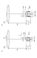
102 第2の撮像素子
103 ビームスプリッタ
500 撮影レンズ
101a、101b、102a、102b、201a、201b、301a、301b 光電変換部
101c、102c、201c、301c マイクロレンズ
EPL 射出瞳
IP 予定結像面
AFPa1、AFPb1、AFPa2、AFPb2、AFPa12、AFPb12、AFPa13、AFPb13 瞳領域
Claims (21)
- 撮影レンズの射出瞳を通過した光束を複数の光束に分割する光束分割手段と、
複数のマイクロレンズを有し前記分割された光束の一方を受光する第1の撮像素子と、
複数のマイクロレンズを有し前記分割された光束の他方を受光する第2の撮像素子と、を有し、
前記第1、第2の撮像素子は、それぞれ各マイクロレンズに対応して、一対の光電変換部を有し、
前記一対の光電変換部が受光する光束がそれぞれ通過する前記射出瞳の一対の瞳領域は、前記第1、第2の撮像素子のいずれでも重複し、
前記第2の撮像素子における前記射出瞳の一対の瞳領域の重心間の距離は前記第1の撮像素子における前記重心間の距離と比べて大きいことを特徴とする撮像装置。 - 前記射出瞳の直径は、前記一対の瞳領域の重心間の距離よりも大きいことを特徴とする請求項1に記載の撮像装置。
- 前記第1の撮像素子の有する前記複数の光電変換部の各面積は、前記第2の撮像素子の有する前記複数の光電変換部の各面積よりも小さいことを特徴とする請求項1又は請求項2に記載の撮像装置。
- 前記第1の撮像素子と前記第2の撮像素子は、
撮影レンズを介して、被写体に対して光学的に共役な結像面にあることを特徴とする請求項1乃至請求項3のいずれか1項に記載の撮像装置。 - 第1及び第2の撮像素子は複数の画素部を有し、
前記第1の撮像素子は前記第2の撮像素子よりも画素数が多いことを特徴とする請求項1乃至請求項4のいずれか1項に記載の撮像装置。 - 前記第1の撮像素子と前記第2の撮像素子において、記録用又は表示用の信号を得るために前記一対の光電変換部の信号を加算する加算制御手段を有することを特徴とする請求項1乃至請求項5のいずれか1項に記載の撮像装置。
- 前記第1の撮像素子から静止画用の画像信号を生成する第1の生成手段と、前記第2の撮像素子から動画用の画像信号を生成する第2の生成手段を有することを特徴とする請求項6に記載の撮像装置。
- 前記第1の生成手段と前記第2の生成手段が並行して画像信号の生成を行うよう制御する第1の制御手段を有する請求項7に記載の撮像装置。
- 前記一対の瞳領域の重心を結んだ線を通る断面についてみたときに、前記一対の瞳領域の受光効率を示す受光効率曲線において、一対の瞳領域ぞれぞれの受光効率曲線で囲まれた領域の面積を足して2で割った面積に対する当該一対の瞳領域の受光効率曲線で囲まれた領域の重複部分の領域の面積の比が重なり比であり、第1の撮像素子における前記一対の瞳領域が重複する部分の重なり比は、第2の撮像素子における前記一対の瞳領域が重複する部分の重なり比とは異なることを特徴とする請求項1乃至請求項8のいずれか1項に記載の撮像装置。
- 第1の撮像素子における重なり比は第2の撮像素子における重なり比よりも大きいことを特徴とする請求項9に記載の撮像装置。
- 前記第1の撮像素子におけるマイクロレンズの焦点位置は、前記第2の撮像素子におけるマイクロレンズの焦点位置よりもマイクロレンズに対して光電変換部の方向に深い位置であることを特徴とする請求項9又は請求項10に記載の撮像装置。
- 前記第1の撮像素子は、前記マイクロレンズと一対の光電変換部との間に光をより効率よく受光するための導波路を有し、前記第2の撮像素子は導波路を有しないことを特徴とする請求項1又は請求項10に記載の撮像装置。
- 前記第1の撮像素子は、裏面照射型CMOSイメージセンサであり、前記第2の撮像素子は表面照射型CMOSイメージセンサであることを特徴とする請求項1乃至請求項10のいずれか1項に記載の撮像装置。
- 前記第1、第2の撮像素子の少なくとも一方から取得した信号を用いて焦点検出する焦点検出手段を有することを特徴とする請求項1乃至請求項13のいずれか1項に記載の撮像装置。
- 前記撮影レンズのFナンバに応じて、前記第1、第2の撮像素子のいずれから信号を取得して焦点検出に選択的に用いるよう制御する第2の制御手段を有することを特徴とする請求項14に記載の撮像装置。
- 前記第1の撮像素子によって画像信号を取得する場合において、前記撮影レンズのFナンバが所定値以下である第1のFナンバである場合には、前記第1の撮像素子から取得した信号を用いて焦点検出を行い、撮影レンズのFナンバが所定値よりも大きい第2のFナンバである場合には、前記第2の撮像素子から取得した信号を用いて焦点検出を行うよう前記第2の制御手段が制御することを特徴とする請求項15に記載の撮像装置。
- 前記第1、第2の撮像素子の少なくとも一方から取得した信号を用いて焦点検出する撮像装置において、取得した画像の空間周波数に応じて、前記第1、第2の撮像素子のいずれかから信号を取得して焦点検出に選択的に用いるよう制御する第3の制御手段を有することを特徴とする請求項3に記載の撮像装置。
- 前記第1又は第2の撮像素子から取得した画像の前記空間周波数が所定値以下である場合には、前記第2の撮像素子から取得した信号を用いて焦点検出を行い、前記空間周波数が所定値よりも大きい場合には、前記第1の撮像素子から取得した信号を用いて焦点検出を行うよう前記第3の制御手段が制御することを特徴とする請求項17に記載の撮像装置。
- 前記第1、第2の撮像素子の少なくとも一方から取得した信号を用いて焦点検出する撮像装置において、
前記第2の撮像素子によって取得した画像が所定レベル以上の高周波成分を含む第1の画像である場合には、前記第1の撮像素子から取得した信号を用いて焦点検出を行い、
前記画像が前記所定レベル以上の高周波成分を含まない第2の画像である場合には、第2の撮像素子から取得した信号を用いて焦点検出を行うよう制御する第4の制御手段を有することを特徴とする請求項3に記載の撮像装置。 - 前記第1、第2の撮像素子のいずれかを選択して選択的に電力を供給する第1の電力供給モードと、前記第1、第2の撮像素子の両方に電力を供給する第2の電力供給モードを有することを特徴とする請求項1乃至請求項19のいずれか1項に記載の撮像装置。
- 撮影レンズを通過した光束を複数の光束に分割する光束分割手段と、
複数のマイクロレンズを有しそれぞれ前記分割された光束の一方を受光する第1の撮像素子と、
前記分割された光束の他方を受光する第2の撮像素子と、を有し、
前記第1、第2の撮像素子は、それぞれ各マイクロレンズに対応して、一対の光電変換部を有し、
前記第1の撮像素子と前記第2の撮像素子のそれぞれにおいて、前記一対の光電変換部のうちそれぞれ一方の光電変換部が受光する光束と、他方の光電変換部が受光する光束とは一部が重複し、
前記第1の撮像素子と前記第2の撮像素子では、前記一方の光電変換部が受光する光束の主光線が通過する射出瞳の領域内の点と前記他方の光電変換部が受光する光束の主光線が通過する射出瞳の領域内の点との間の距離が異なることを特徴とする撮像装置。
Priority Applications (2)
| Application Number | Priority Date | Filing Date | Title |
|---|---|---|---|
| JP2015109420A JP6584149B2 (ja) | 2015-05-29 | 2015-05-29 | 撮像装置 |
| US15/159,673 US9854146B2 (en) | 2015-05-29 | 2016-05-19 | Imaging apparatus with two image sensors |
Applications Claiming Priority (1)
| Application Number | Priority Date | Filing Date | Title |
|---|---|---|---|
| JP2015109420A JP6584149B2 (ja) | 2015-05-29 | 2015-05-29 | 撮像装置 |
Publications (2)
| Publication Number | Publication Date |
|---|---|
| JP2016224208A JP2016224208A (ja) | 2016-12-28 |
| JP6584149B2 true JP6584149B2 (ja) | 2019-10-02 |
Family
ID=57398474
Family Applications (1)
| Application Number | Title | Priority Date | Filing Date |
|---|---|---|---|
| JP2015109420A Expired - Fee Related JP6584149B2 (ja) | 2015-05-29 | 2015-05-29 | 撮像装置 |
Country Status (2)
| Country | Link |
|---|---|
| US (1) | US9854146B2 (ja) |
| JP (1) | JP6584149B2 (ja) |
Families Citing this family (15)
| Publication number | Priority date | Publication date | Assignee | Title |
|---|---|---|---|---|
| WO2017090233A1 (ja) * | 2015-11-24 | 2017-06-01 | パナソニックIpマネジメント株式会社 | 撮像装置 |
| JP6755679B2 (ja) * | 2016-03-04 | 2020-09-16 | キヤノン株式会社 | 撮像装置 |
| JP6748454B2 (ja) * | 2016-03-10 | 2020-09-02 | キヤノン株式会社 | 撮像装置及びその制御方法、プログラム、記憶媒体 |
| US10014338B2 (en) * | 2016-10-12 | 2018-07-03 | Samsung Electronics Co., Ltd. | Image sensor |
| JP6814028B2 (ja) | 2016-11-17 | 2021-01-13 | 上村工業株式会社 | プリント配線基板の製造方法 |
| JP2018169517A (ja) * | 2017-03-30 | 2018-11-01 | ソニーセミコンダクタソリューションズ株式会社 | 撮像装置、撮像モジュールおよび撮像装置の制御方法 |
| FR3065132B1 (fr) * | 2017-04-06 | 2019-06-28 | Office National D'etudes Et De Recherches Aerospatiales (Onera) | Dispositif et procede d'imagerie multispectrale dans l'infrarouge |
| CN106961555B (zh) * | 2017-04-20 | 2019-11-05 | 成都极米科技股份有限公司 | 数据处理方法及装置 |
| JP6946045B2 (ja) * | 2017-04-28 | 2021-10-06 | キヤノン株式会社 | 焦点検出装置及び撮像システム |
| JP6991807B2 (ja) * | 2017-09-20 | 2022-01-13 | キヤノン株式会社 | 撮像装置、その制御方法、および制御プログラム |
| CN107682617A (zh) * | 2017-11-15 | 2018-02-09 | 维沃移动通信有限公司 | 一种摄像头结构及移动终端 |
| JP7066458B2 (ja) * | 2018-03-08 | 2022-05-13 | キヤノン株式会社 | 撮像装置及びその制御方法、プログラム |
| US11714259B2 (en) * | 2018-07-20 | 2023-08-01 | Nikon Corporation | Focus detection device, imaging device, and interchangeable lens |
| CN110166675B (zh) * | 2019-06-14 | 2024-02-13 | 深圳扑浪创新科技有限公司 | 同步拍摄装置与同步拍摄方法 |
| KR20210087809A (ko) * | 2020-01-03 | 2021-07-13 | 삼성전자주식회사 | 이미지 센서를 포함하는 전자 장치 및 그의 동작 방법 |
Family Cites Families (18)
| Publication number | Priority date | Publication date | Assignee | Title |
|---|---|---|---|---|
| JP2754455B2 (ja) * | 1994-05-09 | 1998-05-20 | 株式会社ニコン | 焦点検出装置 |
| US5815748A (en) * | 1996-02-15 | 1998-09-29 | Minolta Co., Ltd. | Camera |
| JP2008070629A (ja) * | 2006-09-14 | 2008-03-27 | Nikon Corp | 光検出装置、カメラ、焦点検出装置および光学特性測定装置 |
| JP4979482B2 (ja) * | 2007-06-28 | 2012-07-18 | オリンパス株式会社 | 撮像装置及び画像信号処理プログラム |
| JP5217880B2 (ja) * | 2008-10-09 | 2013-06-19 | 株式会社ニコン | 撮像装置 |
| JP5434761B2 (ja) * | 2010-04-08 | 2014-03-05 | 株式会社ニコン | 撮像デバイスおよび撮像装置 |
| JP5764884B2 (ja) * | 2010-08-16 | 2015-08-19 | ソニー株式会社 | 撮像素子および撮像装置 |
| JP2012043939A (ja) * | 2010-08-18 | 2012-03-01 | Sony Corp | 撮像素子および撮像装置 |
| JP5861257B2 (ja) * | 2011-02-21 | 2016-02-16 | ソニー株式会社 | 撮像素子および撮像装置 |
| KR101777351B1 (ko) * | 2011-05-16 | 2017-09-11 | 삼성전자주식회사 | 촬상 소자, 이를 이용한 디지털 촬영 장치, 오토 포커싱 방법, 및 상기 방법을 수행하기 위한 컴퓨터 판독가능 저장매체 |
| JP5998583B2 (ja) * | 2012-03-30 | 2016-09-28 | 株式会社ニコン | 撮像装置 |
| JP2014122957A (ja) * | 2012-12-20 | 2014-07-03 | Canon Inc | 撮像装置 |
| US9473688B2 (en) * | 2012-12-20 | 2016-10-18 | Canon Kabushiki Kaisha | Image pickup apparatus comprising a plurality of imaging sensors and image processing units |
| JP6249636B2 (ja) * | 2013-05-28 | 2017-12-20 | キヤノン株式会社 | 撮像装置およびその制御方法 |
| JP2014216970A (ja) * | 2013-04-27 | 2014-11-17 | キヤノン株式会社 | 測距装置 |
| JP2014239290A (ja) * | 2013-06-06 | 2014-12-18 | ソニー株式会社 | 焦点検出装置、電子機器、製造装置、製造方法 |
| JP6207293B2 (ja) * | 2013-08-09 | 2017-10-04 | キヤノン株式会社 | 撮像装置、撮像システム、撮像装置の制御方法、プログラム、および、記憶媒体 |
| JP6021780B2 (ja) * | 2013-10-07 | 2016-11-09 | キヤノン株式会社 | 画像データ処理装置、距離算出装置、撮像装置および画像データ処理方法 |
-
2015
- 2015-05-29 JP JP2015109420A patent/JP6584149B2/ja not_active Expired - Fee Related
-
2016
- 2016-05-19 US US15/159,673 patent/US9854146B2/en active Active
Also Published As
| Publication number | Publication date |
|---|---|
| US9854146B2 (en) | 2017-12-26 |
| JP2016224208A (ja) | 2016-12-28 |
| US20160349522A1 (en) | 2016-12-01 |
Similar Documents
| Publication | Publication Date | Title |
|---|---|---|
| JP6584149B2 (ja) | 撮像装置 | |
| JP5552214B2 (ja) | 焦点検出装置 | |
| JP5169499B2 (ja) | 撮像素子および撮像装置 | |
| JP5207797B2 (ja) | 撮像装置およびその制御方法 | |
| CN107431755B (zh) | 图像处理设备、摄像设备、图像处理方法和存储介质 | |
| JP6381266B2 (ja) | 撮像装置、制御装置、制御方法、プログラム、および、記憶媒体 | |
| US11297271B2 (en) | Image sensor and image capture apparatus | |
| JP2014056014A (ja) | 撮像素子および撮像装置 | |
| JP2019041178A (ja) | 撮像素子およびこの撮像素子を用いた撮像装置 | |
| JP2010128205A (ja) | 撮像装置 | |
| JP6271911B2 (ja) | 撮像装置及びその制御方法、デフォーカス量算出方法 | |
| JP2017032646A (ja) | 撮像装置及びその制御方法 | |
| JP2017118212A (ja) | 撮像装置 | |
| JP5796388B2 (ja) | 焦点検出装置および撮像装置 | |
| JP5929060B2 (ja) | 焦点検出装置および撮像装置 | |
| JP5891667B2 (ja) | 焦点調節装置およびそれを備えた撮像装置 | |
| JP2020171050A (ja) | 画像処理装置、撮像装置、画像処理方法、および、記憶媒体 | |
| JP6639208B2 (ja) | 撮像装置及びその制御方法 | |
| JP2016071275A (ja) | 撮像装置およびフォーカス制御プログラム | |
| JP2014211589A (ja) | 焦点調節装置および撮像装置 | |
| JP2009031562A (ja) | 受光素子、受光装置、焦点検出装置、カメラ | |
| JP7022534B2 (ja) | 画像処理装置および画像処理方法 | |
| JP6628617B2 (ja) | 画像処理装置及び画像処理方法 | |
| JP6714434B2 (ja) | 撮像装置およびその制御方法、プログラム、記憶媒体 | |
| JP6378526B2 (ja) | 撮像装置及びその制御方法 |
Legal Events
| Date | Code | Title | Description |
|---|---|---|---|
| A621 | Written request for application examination |
Free format text: JAPANESE INTERMEDIATE CODE: A621 Effective date: 20180524 |
|
| A977 | Report on retrieval |
Free format text: JAPANESE INTERMEDIATE CODE: A971007 Effective date: 20181218 |
|
| A131 | Notification of reasons for refusal |
Free format text: JAPANESE INTERMEDIATE CODE: A131 Effective date: 20190205 |
|
| A521 | Request for written amendment filed |
Free format text: JAPANESE INTERMEDIATE CODE: A523 Effective date: 20190405 |
|
| TRDD | Decision of grant or rejection written | ||
| A01 | Written decision to grant a patent or to grant a registration (utility model) |
Free format text: JAPANESE INTERMEDIATE CODE: A01 Effective date: 20190806 |
|
| A61 | First payment of annual fees (during grant procedure) |
Free format text: JAPANESE INTERMEDIATE CODE: A61 Effective date: 20190903 |
|
| R151 | Written notification of patent or utility model registration |
Ref document number: 6584149 Country of ref document: JP Free format text: JAPANESE INTERMEDIATE CODE: R151 |
|
| LAPS | Cancellation because of no payment of annual fees |