JP6583073B2 - Temperature sensor - Google Patents
Temperature sensor Download PDFInfo
- Publication number
- JP6583073B2 JP6583073B2 JP2016052659A JP2016052659A JP6583073B2 JP 6583073 B2 JP6583073 B2 JP 6583073B2 JP 2016052659 A JP2016052659 A JP 2016052659A JP 2016052659 A JP2016052659 A JP 2016052659A JP 6583073 B2 JP6583073 B2 JP 6583073B2
- Authority
- JP
- Japan
- Prior art keywords
- pair
- insulating film
- connection
- lead frames
- sensor
- Prior art date
- Legal status (The legal status is an assumption and is not a legal conclusion. Google has not performed a legal analysis and makes no representation as to the accuracy of the status listed.)
- Active
Links
- 239000000758 substrate Substances 0.000 claims description 54
- 230000001681 protective effect Effects 0.000 claims description 17
- 239000000463 material Substances 0.000 claims description 6
- 239000010408 film Substances 0.000 description 75
- 229920001721 polyimide Polymers 0.000 description 7
- 239000010409 thin film Substances 0.000 description 6
- 238000000034 method Methods 0.000 description 5
- 238000003466 welding Methods 0.000 description 5
- 238000005259 measurement Methods 0.000 description 4
- 238000000059 patterning Methods 0.000 description 4
- 238000007747 plating Methods 0.000 description 4
- 238000004544 sputter deposition Methods 0.000 description 4
- RYGMFSIKBFXOCR-UHFFFAOYSA-N Copper Chemical compound [Cu] RYGMFSIKBFXOCR-UHFFFAOYSA-N 0.000 description 3
- 239000007789 gas Substances 0.000 description 3
- 238000004519 manufacturing process Methods 0.000 description 3
- 239000011347 resin Substances 0.000 description 3
- 229920005989 resin Polymers 0.000 description 3
- 229910000679 solder Inorganic materials 0.000 description 3
- IJGRMHOSHXDMSA-UHFFFAOYSA-N Atomic nitrogen Chemical compound N#N IJGRMHOSHXDMSA-UHFFFAOYSA-N 0.000 description 2
- 239000004642 Polyimide Substances 0.000 description 2
- 239000000853 adhesive Substances 0.000 description 2
- 230000001070 adhesive effect Effects 0.000 description 2
- 230000015572 biosynthetic process Effects 0.000 description 2
- 239000011889 copper foil Substances 0.000 description 2
- 229910001873 dinitrogen Inorganic materials 0.000 description 2
- 238000010438 heat treatment Methods 0.000 description 2
- 239000012528 membrane Substances 0.000 description 2
- 229920003207 poly(ethylene-2,6-naphthalate) Polymers 0.000 description 2
- 239000011112 polyethylene naphthalate Substances 0.000 description 2
- -1 polyethylene terephthalate Polymers 0.000 description 2
- 229920000139 polyethylene terephthalate Polymers 0.000 description 2
- 239000005020 polyethylene terephthalate Substances 0.000 description 2
- 239000004809 Teflon Substances 0.000 description 1
- 229920006362 Teflon® Polymers 0.000 description 1
- 229910004349 Ti-Al Inorganic materials 0.000 description 1
- 229910010037 TiAlN Inorganic materials 0.000 description 1
- 229910004692 Ti—Al Inorganic materials 0.000 description 1
- 229910045601 alloy Inorganic materials 0.000 description 1
- 239000000956 alloy Substances 0.000 description 1
- PNEYBMLMFCGWSK-UHFFFAOYSA-N aluminium oxide Inorganic materials [O-2].[O-2].[O-2].[Al+3].[Al+3] PNEYBMLMFCGWSK-UHFFFAOYSA-N 0.000 description 1
- 239000011324 bead Substances 0.000 description 1
- 239000010949 copper Substances 0.000 description 1
- 238000005260 corrosion Methods 0.000 description 1
- 230000007797 corrosion Effects 0.000 description 1
- 230000008878 coupling Effects 0.000 description 1
- 238000010168 coupling process Methods 0.000 description 1
- 238000005859 coupling reaction Methods 0.000 description 1
- 239000013078 crystal Substances 0.000 description 1
- 230000000694 effects Effects 0.000 description 1
- 238000005516 engineering process Methods 0.000 description 1
- NBVXSUQYWXRMNV-UHFFFAOYSA-N fluoromethane Chemical compound FC NBVXSUQYWXRMNV-UHFFFAOYSA-N 0.000 description 1
- 238000009413 insulation Methods 0.000 description 1
- 238000010030 laminating Methods 0.000 description 1
- 229910052751 metal Inorganic materials 0.000 description 1
- 239000002184 metal Substances 0.000 description 1
- 238000012986 modification Methods 0.000 description 1
- 230000004048 modification Effects 0.000 description 1
- 229910001120 nichrome Inorganic materials 0.000 description 1
- 238000005121 nitriding Methods 0.000 description 1
- QJGQUHMNIGDVPM-UHFFFAOYSA-N nitrogen group Chemical group [N] QJGQUHMNIGDVPM-UHFFFAOYSA-N 0.000 description 1
- 229910000510 noble metal Inorganic materials 0.000 description 1
- 239000009719 polyimide resin Substances 0.000 description 1
- 238000003825 pressing Methods 0.000 description 1
- 238000007639 printing Methods 0.000 description 1
- 238000005546 reactive sputtering Methods 0.000 description 1
- 230000004043 responsiveness Effects 0.000 description 1
- 238000005477 sputtering target Methods 0.000 description 1
- 239000002966 varnish Substances 0.000 description 1
- 238000001039 wet etching Methods 0.000 description 1
- 229910052984 zinc sulfide Inorganic materials 0.000 description 1
Images


Landscapes
- Measuring Temperature Or Quantity Of Heat (AREA)
- Thermistors And Varistors (AREA)
Description
本発明は、複写機やプリンタ等の定着ローラの温度を測定することに好適な温度センサに関する。 The present invention relates to a temperature sensor suitable for measuring the temperature of a fixing roller of a copying machine or a printer.
一般に、複写機やプリンタ等の画像形成装置に使用されている定着ローラ(加熱ローラ)には、その温度を測定するために温度センサが接触状態に設置されている。このような温度センサとしては、例えば特許文献1に、一対のリードフレームと、これらのリードフレームの間に配設され接続された感熱素子と、一対のリードフレームの端部に形成された保持部と、リードフレーム及び感熱素子の片面に設けられ定着ローラに接触させる保護テープとを有する温度センサが提案されている。
上記特許文献1には、感熱素子として ビードサーミスタやチップサーミスタの他に、アルミナ等の絶縁基板の一面に感熱膜が形成された薄膜サーミスタが採用されている。
Generally, a fixing roller (heating roller) used in an image forming apparatus such as a copying machine or a printer is provided with a temperature sensor in contact with the fixing roller (heating roller). As such a temperature sensor, for example, in Patent Document 1, a pair of lead frames, a thermal element disposed and connected between the lead frames, and a holding portion formed at an end portion of the pair of lead frames. And a temperature sensor having a lead frame and a protective tape provided on one side of the thermal element and brought into contact with the fixing roller.
In Patent Document 1, a thin film thermistor in which a heat sensitive film is formed on one surface of an insulating substrate such as alumina is employed in addition to a bead thermistor and a chip thermistor as a heat sensitive element.
また、近年、柔軟性に優れると共に全体を薄くすることができるフィルム型温度センサとして、絶縁性フィルム上に薄膜サーミスタを形成した温度センサが開発されている。例えば、特許文献2には、一対のリードフレームと、一対のリードフレームに接続されたセンサ部と、一対のリードフレームに固定されてリードフレームを保持する絶縁性の保持部とを備えた温度センサが提案されている。
In recent years, a temperature sensor in which a thin film thermistor is formed on an insulating film has been developed as a film-type temperature sensor that is excellent in flexibility and can be thinned as a whole. For example,
この温度センサは、センサ部が、絶縁性フィルムと、該絶縁性フィルムの表面にサーミスタ材料でパターン形成された薄膜サーミスタ部と、薄膜サーミスタ部の上及び下の少なくとも一方に複数の櫛部を有して互いに対向してパターン形成された一対の櫛型電極と、一対の櫛型電極に接続され絶縁性フィルムの表面にパターン形成された一対のパターン電極とを備え、一対のリードフレームが、絶縁性フィルムの表面に薄膜サーミスタ部を間に配して延在して接着されていると共に一対のパターン電極に接続されている。 In this temperature sensor, the sensor unit has an insulating film, a thin film thermistor portion patterned with the thermistor material on the surface of the insulating film, and a plurality of comb portions above and below the thin film thermistor portion. A pair of comb electrodes patterned to face each other, and a pair of pattern electrodes connected to the pair of comb electrodes and patterned on the surface of the insulating film. A thin film thermistor portion is extended and bonded to the surface of the film, and is connected to a pair of pattern electrodes.
上記従来の技術には、以下の課題が残されている。
特許文献2に記載の技術では、一対のリードフレームの間隔よりも広い絶縁性フィルムを用いて一対のリードフレームにセンサ部を接着しているため、大きな面積のセンサ部が必要になっていた。応答性の向上や部材コストの低減を図るためにセンサ部を小型化する場合、一対のリードフレームの間隔よりも小さいセンサ部にするとリードフレームとの接続が困難になるという不都合が生じる。また、比較的小さいセンサ部を一対のリードフレーム上に直接、設置した場合、センサ部がリードフレーム上の段差部となり、定着ローラへの接触面に段差が生じることになって定着ローラに対して安定して正確に接触させ難いという不都合があった。
The following problems remain in the conventional technology.
In the technique described in
本発明は、前述の課題に鑑みてなされたもので、センサ部の小型化が可能であると共に測定対象物に対して安定して正確に接触させることができる温度センサを提供することを目的とする。 The present invention has been made in view of the above-described problems, and an object of the present invention is to provide a temperature sensor that can reduce the size of a sensor unit and can stably and accurately contact an object to be measured. To do.
本発明は、前記課題を解決するために以下の構成を採用した。すなわち、第1の発明に係る温度センサは、一対のリードフレームと、一対の前記リードフレームの先端側に接続された連結用基板と、前記連結用基板に接続され感熱素子を有するセンサ部と、前記一対のリードフレームの基端側に固定されて一対の前記リードフレームを保持する絶縁性の保持部とを備え、前記センサ部が、絶縁性フィルムと、前記絶縁性フィルムの一方の面に設けられサーミスタ材料で形成されたサーミスタ部と、前記サーミスタ部に接続された一対の対向電極と、一端が一対の前記対向電極に接続されていると共に前記絶縁性フィルムの一方の面に形成された一対の接続電極とを備え、前記連結用基板が、基板本体と、一端が一対の前記リードフレームの先端側における一方の面に接続され他端が一対の前記リードフレームの間に配されて一対の前記接続電極の他端に接続され前記基板本体上に形成された一対の連結用配線膜とを備え、前記センサ部が、一対の前記リードフレームの間に配されて前記リードフレームの他方の面と前記絶縁性フィルムの他方の面とが面一に配されていることを特徴とする。 The present invention employs the following configuration in order to solve the above problems. That is, a temperature sensor according to the first invention includes a pair of lead frames, a connection substrate connected to the tip side of the pair of lead frames, a sensor unit connected to the connection substrate and having a thermal element, An insulating holding portion that is fixed to a base end side of the pair of lead frames and holds the pair of lead frames, and the sensor portion is provided on one surface of the insulating film and the insulating film. a thermistor portion formed by the thermistor material is a pair of a pair of opposed electrodes connected to the thermistor section, one end formed on one surface of the insulating film with which is connected to a pair of the counter electrode The connection substrate is connected to the substrate body, and one end of the pair of lead frames is connected to one surface of the lead frame, and the other end is connected to the pair of lead frames. A pair of connecting wiring films formed on the substrate body and connected to the other ends of the pair of connection electrodes, and the sensor unit is disposed between the pair of lead frames. The other surface of the lead frame and the other surface of the insulating film are arranged flush with each other.
本発明の温度センサでは、連結用基板を介してリードフレームに接続されたセンサ部が、一対のリードフレームの間に配されてリードフレームの他方の面と絶縁性フィルムの他方の面とが面一に配されているので、測定対象物への接触面となる絶縁性フィルムの他方の面側がリードフレームの他方の面と共に平坦面を構成し、測定対象物に対して安定して正確に接触させることができる。また、センサ部自体は、一対のリードフレーム間に収まる小さいサイズに小型化することが可能になる。 In the temperature sensor of the present invention, the sensor portion connected to the lead frame via the connecting substrate is disposed between the pair of lead frames, and the other surface of the lead frame and the other surface of the insulating film are the surfaces. Since the other side of the insulating film, which is the contact surface to the measurement object, forms a flat surface together with the other surface of the lead frame, it contacts the measurement object stably and accurately. Can be made. Further, the sensor unit itself can be miniaturized to a small size that fits between the pair of lead frames.
第2の発明に係る温度センサは、第1の温度センサにおいて、前記連結用基板が、フレキシブルプリント配線板であることを特徴とする。
すなわち、この温度センサでは、連結用基板が、フレキシブルプリント配線板であるので、フレキシブルなセンサ部と共に連結用基板も柔軟性を有することで、測定対象物に押し当てた際に、より柔軟に湾曲して接触させることが可能になる。
A temperature sensor according to a second invention is characterized in that, in the first temperature sensor, the connection board is a flexible printed wiring board.
That is, in this temperature sensor, since the connecting board is a flexible printed wiring board, the connecting board has flexibility as well as the flexible sensor part, so that it can be bent more flexibly when pressed against the measuring object. Can be brought into contact with each other.
第3の発明に係る温度センサは、第1又は第2の発明において、前記センサ部が、前記接続電極の前記連結用配線膜との接続部を除いて前記サーミスタ部及び前記対向電極を覆って前記絶縁性フィルム上に形成された絶縁性の保護膜を備え、前記連結用基板が、少なくとも前記リードフレーム及び前記接続電極との接続部を除いて前記連結用配線膜を覆って前記基板本体上に形成された絶縁性膜を備えていることを特徴とする。
すなわち、この温度センサでは、連結用基板が、少なくともリードフレーム及び接続電極との接続部を除いて連結用配線膜を覆って基板本体上に形成された絶縁性膜を備えているので、連結用配線膜が水分で腐食することを抑制して耐湿性を向上させることができる。
A temperature sensor according to a third invention is the temperature sensor according to the first or second invention, wherein the sensor part covers the thermistor part and the counter electrode except for a connection part between the connection electrode and the connection wiring film. An insulating protective film formed on the insulating film, wherein the connection substrate covers at least the connection wiring film except for a connection portion between the lead frame and the connection electrode; And an insulating film formed on the substrate.
That is, in this temperature sensor, the connecting substrate includes an insulating film formed on the substrate body so as to cover the connecting wiring film except at least the connection portion between the lead frame and the connecting electrode. Moisture resistance can be improved by suppressing corrosion of the wiring film with moisture.
本発明によれば、以下の効果を奏する。
すなわち、本発明に係る温度センサによれば、連結用基板を介してリードフレームに接続されたセンサ部が、一対のリードフレームの間に配されてリードフレームの他方の面と絶縁性フィルムの他方の面とが面一に配されているので、センサ部自体の小型化が可能であると共に、絶縁性フィルムの他方の面側がリードフレームの他方の面と共に平坦面を構成し、測定対象物に対して安定して正確に接触させることができる。
したがって、本発明の温度センサによれば、平坦面を測定対象物に押し当ることで、より安定して正確な温度測定が可能になり、複写機やプリンタ等の定着ローラの温度測定用の温度センサとして好適である。
The present invention has the following effects.
That is, according to the temperature sensor of the present invention, the sensor portion connected to the lead frame via the connecting substrate is disposed between the pair of lead frames, and the other surface of the lead frame and the other of the insulating film. The sensor part itself can be reduced in size, and the other surface side of the insulating film constitutes a flat surface together with the other surface of the lead frame, so that the object to be measured can be reduced. In contrast, the contact can be made stably and accurately.
Therefore, according to the temperature sensor of the present invention, it is possible to measure the temperature more stably and accurately by pressing the flat surface against the object to be measured. It is suitable as a sensor.
以下、本発明に係る温度センサにおける一実施形態を、図1から図8を参照しながら説明する。なお、以下の説明に用いる図面の一部では、各部を認識可能又は認識容易な大きさとするために必要に応じて縮尺を適宜変更している。 Hereinafter, an embodiment of a temperature sensor according to the present invention will be described with reference to FIGS. Note that in some of the drawings used for the following description, the scale is appropriately changed as necessary to make each part recognizable or easily recognizable.
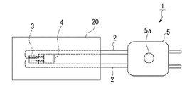
本実施形態の温度センサ1は、図1に示すように、一対のリードフレーム2と、一対のリードフレーム2の先端側に接続された連結用基板3と、連結用基板3に接続され感熱素子を有するセンサ部4と、一対のリードフレーム2の基端側に固定されて一対のリードフレーム2を保持する絶縁性の保持部5とを備えている。
As shown in FIG. 1, the temperature sensor 1 according to the present embodiment includes a pair of
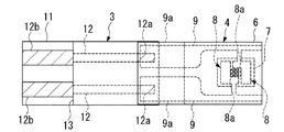
上記センサ部4は、図2に示すように、絶縁性フィルム6と、絶縁性フィルム6の一方の面に設けられサーミスタ材料で形成されたサーミスタ部7と、サーミスタ部7に接続された一対の対向電極8と、一端が一対の対向電極8に接続されていると共に絶縁性フィルム6の一方の面に形成された一対の接続電極9とを備えている。
The
上記連結用基板3は、図3に示すように、基板本体11と、一端が一対のリードフレーム2の先端側における一方の面に接続され他端が一対のリードフレーム2の間に配されて一対の接続電極9の他端に接続され基板本体11上に形成された一対の連結用配線膜12とを備えている。
また、センサ部4は、一対のリードフレーム2の間に配されてリードフレーム2の他方の面と絶縁性フィルム6の他方の面とが面一に配されている。
As shown in FIG. 3, the connecting
The
上記連結用基板3は、フレキシブルプリント配線板である。すなわち、基板本体11は、ポリイミドフィルムで形成され、連結用配線膜12はCu箔あるいはCuめっき膜で形成されている。なお、基板本体11の幅は、一対のリードフレーム2の先端部2aの間隔よりも広く、かつ一対のリードフレーム2の基端側の間隔よりも小さく設定されている。
上記センサ部4は、接続電極9の連結用配線膜12との接続部であるパッド部9aを除いてサーミスタ部7及び対向電極8を覆って絶縁性フィルム6上に形成された絶縁性の保護膜10を備えている。
また、本実施形態の温度センサ1は、一対のリードフレーム2とセンサ部4とを上下から挟んで互いに接着された一対の絶縁性の保護テープ20を備えている。
The
The
Further, the temperature sensor 1 of the present embodiment includes a pair of insulating
上記連結用基板3は、少なくともフレーム側接続部12b及びセンサ側接続部12aを除いて連結用配線膜12を覆って基板本体11上に形成された絶縁性膜13を備えている。この絶縁性膜13は、例えば厚さ15μmのレジスト膜である。
上記連結用配線膜12は、例えば厚さ18μmの銅箔である。また、連結用配線膜12のセンサ側接続部12a及びフレーム側接続部12bは、銅箔上に厚さ3μmのNiめっき膜及び厚さ0.05μmのAuめっき膜が積層されている。
The connecting
The connecting
一対のリードフレーム2は、図5に示すように、保持部5から互いに平行に延在しており、その先端部2aは、基端側に比べて互いに内側に幅広な形状とされている。
なお、保持部5には、取付孔5aが形成されている。
一対の上記接続電極9の先端側(他端側)には、幅広なパッド部9aが形成されている。これらのパッド部9aに、図6に示すように、連結用基板3のセンサ側接続部12aが、ハンダ接合により接着されている。
As shown in FIG. 5, the pair of
The holding
A
また、連結用基板3のフレーム側接続部12bは、リードフレーム2の先端部2aに、抵抗溶接、スポット溶接、ハンダ材又は導電性樹脂接着剤等の接着剤により接着されている。特に、溶接によってフレーム側接続部12bとリードフレーム2の先端部2aとを接合する場合、連結用配線12の厚さが、センサ部4のパッド部9aよりも厚く形成されていることで、センサ部4のパッド部9aとリードフレーム2の先端部2aとを直接溶接した場合よりも、高い溶接強度を得ることができる。
なお、センサ部4では、パッド部9aを除いた接続電極9,サーミスタ部7及び対向電極8を覆う絶縁性の保護膜10が絶縁性フィルム6上に形成されている。
Further, the frame
In the
上記絶縁性フィルム6は、略長方形状とされ、例えば厚さ7.5〜125μmのポリイミド樹脂シートで帯状に形成されている。この絶縁性フィルム6の幅は、一対のリードフレーム2の基端側の間隔よりも小さく設定されている。
なお、絶縁性フィルム6としては、他にPET:ポリエチレンテレフタレート,PEN:ポリエチレンナフタレート等でも作製できるが、定着ローラの温度測定用としては、最高使用温度が230℃と高いためポリイミドフィルムが望ましい。
The said insulating
The insulating
上記サーミスタ部7は、パターン形成された薄膜サーミスタであり、絶縁性フィルム6の基端側に配され、例えばTiAlNのサーミスタ材料で形成されている。特に、サーミスタ部7は、一般式:TixAlyNz(0.70≦y/(x+y)≦0.95、0.4≦z≦0.5、x+y+z=1)で示される金属窒化物からなり、その結晶構造が、六方晶系のウルツ鉱型の単相である。
The
上記接続電極9及び対向電極8は、サーミスタ部7上に形成された膜厚5〜100nmのCr又はNiCrの接合層と、該接合層上にAu等の貴金属で膜厚50〜1000nmで形成された電極層とを有している。
上記対向電極8は、サーミスタ部7の上に複数の櫛部8aを有して互いに対向してパターン形成されている。
すなわち、一対の対向電極8は、互いに対向状態に配されて交互に櫛部8aが並んだ櫛型パターンとされている。
このように、絶縁性フィルム6、サーミスタ部7、対向電極8及び接続電極9によって感熱素子が構成されている。
The
The
That is, the pair of
As described above, the insulating
上記保護膜10は、絶縁性樹脂膜等であり、例えば厚さ15μmのポリイミド膜が採用される。
上記保護テープ20は、テフロン(登録商標)等のフッ化炭素樹脂で形成されている。
なお、本実施形態では、センサ部4が直接リードフレーム2に接着されていない分、従来に比べて保護テープ20がリードフレーム2に接する面積を大きくでき、保護テープ20の高い接着性が得られることで剥がれ等を抑制することができる。
The
The
In the present embodiment, since the
上記リードフレームの厚さは、例えば0.8mmとされ、絶縁性フィルム6の厚さも同じ0.8mmとされる。すなわち、図8に示すように、リードフレーム2に連結用基板3を介して接続されたセンサ部4の他方の面は、リードフレーム2の他方の面と面一になるように設定されている。
The lead frame has a thickness of, for example, 0.8 mm, and the insulating
本実施形態の温度センサ1の製造方法は、絶縁性フィルム6の表面にサーミスタ部7をパターン形成するサーミスタ部形成工程と、互いに対向した一対の対向電極8をサーミスタ部7上に配して絶縁性フィルム6の表面に一対の接続電極9をパターン形成する電極形成工程と、絶縁性フィルム6上に保護膜10を形成する保護膜形成工程と、センサ部4と連結用基板3とを接続する基板接続工程と、連結用基板3とリードフレーム2とを固定するリードフレーム固定工程と、リードフレーム2、連結用基板3及びセンサ部4を上下から保護テープ20で挟んで互いに接着する保護テープ接着工程とを有している。
The manufacturing method of the temperature sensor 1 of the present embodiment includes a thermistor part forming step of patterning the
より具体的な製造方法の例としては、厚さ75μmのポリイミドフィルムの絶縁性フィルム6上(一方の面上)に、Ti−Al合金スパッタリングターゲットを用い、窒素含有雰囲気中で反応性スパッタ法にて、TixAlyNz(x=0.09、y=0.43、z=0.48)のサーミスタ膜を膜厚200nmで形成する。その時のスパッタ条件は、到達真空度5×10⁻⁶Pa、スパッタガス圧0.4Pa、ターゲット投入電力(出力)200Wで、Arガス+窒素ガスの混合ガス雰囲気下において、窒素ガス分率を20%で作製する。 As a more specific example of the manufacturing method, a reactive sputtering method is performed in a nitrogen-containing atmosphere using a Ti—Al alloy sputtering target on the insulating film 6 (on one surface) of a polyimide film having a thickness of 75 μm. Te, Ti x Al y N z ( x = 0.09, y = 0.43, z = 0.48) is formed by a thermistor film thickness 200nm of. The sputtering conditions at that time were an ultimate vacuum of 5 × 10 −6 Pa, a sputtering gas pressure of 0.4 Pa, a target input power (output) of 200 W, and a nitrogen gas fraction of 20 in a mixed gas atmosphere of Ar gas + nitrogen gas. %.
成膜したサーミスタ膜の上にレジスト液をスピンコーターで塗布した後、110℃で1分30秒プリベークを行い、露光装置で感光後、現像液で不要部分を除去し、さらに150℃で5分のポストベークにてパターニングを行う。その後、不要なTixAlyNzのサーミスタ膜を市販のTiエッチャントでウェットエッチングを行い、図4の(a)に示すように、レジスト剥離にて所望の形状のサーミスタ部7にする。
A resist solution is applied onto the formed thermistor film by a spin coater, pre-baked at 110 ° C. for 1 minute 30 seconds, exposed to light with an exposure device, and unnecessary portions are removed with a developer, and further at 150 ° C. for 5 minutes. Patterning is performed by post-baking. Thereafter, the thermistor film unnecessary Ti x Al y N z by wet etching in a commercial Ti etchant, as shown in FIG. 4 (a), to the
次に、サーミスタ部7及び絶縁性フィルム6上に、スパッタ法にて、Cr膜の接合層を膜厚20nm形成する。さらに、この接合層上に、スパッタ法にてAu膜の電極層を膜厚200nm形成する。
次に、成膜した電極層の上にレジスト液をスピンコーターで塗布した後、110℃で1分30秒プリベークを行い、露光装置で感光後、現像液で不要部分を除去し、150℃で5分のポストベークにてパターニングを行う。その後、不要な電極部分を市販のAuエッチャント及びCrエッチャントの順番でウェットエッチングを行い、図4の(b)に示すように、レジスト剥離にて所望の対向電極8及び接続電極9を形成する。
Next, a 20 nm-thick Cr film bonding layer is formed on the
Next, after applying a resist solution on the electrode layer formed by a spin coater, pre-baking is performed at 110 ° C. for 1 minute and 30 seconds, and after exposure with an exposure apparatus, unnecessary portions are removed with a developer, and at 150 ° C. Patterning is performed by post-baking for 5 minutes. Thereafter, unnecessary electrode portions are wet-etched in the order of commercially available Au etchant and Cr etchant, and as shown in FIG. 4B, desired
次に、絶縁性フィルム6の表面にポリイミドワニスを印刷法により所定部分に塗布して、180℃、30分でキュアを行い、図4の(c)に示すように、15μm厚のポリイミド保護膜10を形成する。
次に、パッド部9aとなる幅広な領域にNiめっきを施して、パッド部9aを形成する。
なお、複数のセンサ部4を同時に作製する場合、絶縁性フィルム6の大判シートに複数のサーミスタ部7、対向電極8、接続電極9、保護膜10及びパッド部9aを上述のように形成した後に、大判シートから各センサ部4に切断する。
Next, a polyimide varnish is applied to the surface of the insulating
Next, Ni plating is performed on a wide region to be the
In addition, when producing the
次に、図6に示すように、連結用基板3とセンサ部4とを接合させる。すなわち、連結用基板3のセンサ側接続部12aとセンサ部4のパッド部9aとを互いに向かい合わせてハンダ接合する。すなわち、連結用基板3の連結用配線12の形成面とセンサ部4の接続電極9の形成面とを互いに向かい合わせて、センサ側接続部12aとパッド部9aとをハンダで接合させる。
Next, as shown in FIG. 6, the connecting
さらに、図1に示すように、接合された連結用基板3及びセンサ部4をリードフレーム2の先端部2aに取り付ける。すなわち、一対のフレーム側接続部12bに一対のリードフレーム2の先端部2aを抵抗溶接等により接着し、リードフレーム2と連結用基板3及びセンサ部4に固定する。
Further, as shown in FIG. 1, the joined
このように連結用基板3を介してリードフレーム2に取り付けられたセンサ部4は、図7及び図8に示すように、一対のリードフレーム2の間に配された状態で、絶縁性フィルム6の他方の面(サーミスタ部7を形成した面の反対面)とリードフレーム2の他方の面(連結用基板3を接着した面の反対面)とが面一となる。
最後に、センサ部4と連結用基板3とリードフレーム2の先端側とを上下から一対の保護テープ20で挟んで、一対の保護テープ20をプレスして接着することで、本実施形態の温度センサ1が作製される。
Thus, the
Finally, the pair of
このように本実施形態の温度センサ1では、連結用基板3を介してリードフレーム2に接続されたセンサ部4が、一対のリードフレーム2の間に配されてリードフレーム2の他方の面と絶縁性フィルム6の他方の面とが面一に配されているので、測定対象物への接触面となる絶縁性フィルム6の他方の面側がリードフレーム2の他方の面と共に平坦面を構成し、測定対象物に対して安定して正確に接触させることができる。また、センサ部4自体は、一対のリードフレーム2間に収まる小さいサイズに小型化することが可能になる。
As described above, in the temperature sensor 1 according to the present embodiment, the
また、連結用基板3が、フレキシブルプリント配線板であるので、フレキシブルなセンサ部4と共に連結用基板3も柔軟性を有することで、定着ローラ等の測定対象物に押し当てた際に、より柔軟に湾曲して接触させることが可能になる。
さらに、連結用基板3が、少なくともリードフレーム2との接続部12a及び接続電極9との12bを除いて連結用配線膜12を覆って基板本体11上に形成された絶縁性膜13を備えているので、連結用配線膜12が水分で腐食することを抑制して耐湿性を向上させることができる。
In addition, since the connecting
Furthermore, the connecting
なお、本発明の技術範囲は上記実施形態に限定されるものではなく、本発明の趣旨を逸脱しない範囲において種々の変更を加えることが可能である。 The technical scope of the present invention is not limited to the above embodiment, and various modifications can be made without departing from the spirit of the present invention.
1…温度センサ、2…リードフレーム、3…連結用基板、4…センサ部、5…保持部、6…絶縁性フィルム、7…サーミスタ部、8…対向電極、9…接続電極、10…保護膜、11…基板本体、12…連結用配線膜、12a…センサ側接続部、12b…フレーム側接続部、13…絶縁性膜 DESCRIPTION OF SYMBOLS 1 ... Temperature sensor, 2 ... Lead frame, 3 ... Connection board, 4 ... Sensor part, 5 ... Holding part, 6 ... Insulating film, 7 ... Thermistor part, 8 ... Counter electrode, 9 ... Connection electrode, 10 ... Protection Membrane, 11 ... substrate body, 12 ... connection wiring film, 12a ... sensor side connection portion, 12b ... frame side connection portion, 13 ... insulating film
Claims (3)
前記センサ部が、絶縁性フィルムと、
前記絶縁性フィルムの一方の面に設けられサーミスタ材料で形成されたサーミスタ部と、
前記サーミスタ部に接続された一対の対向電極と、
一端が一対の前記対向電極に接続されていると共に前記絶縁性フィルムの一方の面に形成された一対の接続電極とを備え、
前記連結用基板が、基板本体と、一端が一対の前記リードフレームの先端側における一方の面に接続され他端が一対の前記リードフレームの間に配されて一対の前記接続電極の他端に接続され前記基板本体上に形成された一対の連結用配線膜とを備え、
前記センサ部が、一対の前記リードフレームの間に配されて前記リードフレームの他方の面と前記絶縁性フィルムの他方の面とが面一に配されていることを特徴とする温度センサ。 A pair of lead frames, a connecting substrate connected to the distal end side of the pair of lead frames, a sensor unit connected to the connecting substrate and having a thermal element, and fixed to the base end side of the pair of lead frames And an insulating holding part that holds the pair of lead frames,
The sensor part is an insulating film;
A thermistor portion formed of a thermistor material provided on one surface of the insulating film,
A pair of counter electrodes connected to the thermistor section;
One end is connected to the pair of counter electrodes and a pair of connection electrodes formed on one surface of the insulating film,
The connecting substrate has a substrate body, one end connected to one surface of the pair of lead frames on the front end side, and the other end arranged between the pair of lead frames to the other end of the pair of connection electrodes. A pair of connecting wiring films connected and formed on the substrate body,
The temperature sensor, wherein the sensor section is disposed between the pair of lead frames, and the other surface of the lead frame and the other surface of the insulating film are disposed flush with each other.
前記連結用基板が、フレキシブルプリント配線板であることを特徴とする温度センサ。 The temperature sensor according to claim 1,
The temperature sensor, wherein the connecting substrate is a flexible printed wiring board.
前記センサ部が、前記接続電極の前記連結用配線膜との接続部を除いて前記サーミスタ部及び前記対向電極を覆って前記絶縁性フィルム上に形成された絶縁性の保護膜を備え、
前記連結用基板が、少なくとも前記リードフレーム及び前記接続電極との接続部を除いて前記連結用配線膜を覆って前記基板本体上に形成された絶縁性膜を備えていることを特徴とする温度センサ。 The temperature sensor according to claim 1 or 2,
The sensor portion includes an insulating protective film formed on the insulating film so as to cover the thermistor portion and the counter electrode except for a connection portion between the connection electrode and the connection wiring film,
The connecting substrate includes an insulating film formed on the substrate body so as to cover the connecting wiring film except at least a connection portion between the lead frame and the connection electrode. Sensor.
Priority Applications (1)
| Application Number | Priority Date | Filing Date | Title |
|---|---|---|---|
| JP2016052659A JP6583073B2 (en) | 2016-03-16 | 2016-03-16 | Temperature sensor |
Applications Claiming Priority (1)
| Application Number | Priority Date | Filing Date | Title |
|---|---|---|---|
| JP2016052659A JP6583073B2 (en) | 2016-03-16 | 2016-03-16 | Temperature sensor |
Publications (3)
| Publication Number | Publication Date |
|---|---|
| JP2017166988A JP2017166988A (en) | 2017-09-21 |
| JP2017166988A5 JP2017166988A5 (en) | 2018-01-18 |
| JP6583073B2 true JP6583073B2 (en) | 2019-10-02 |
Family
ID=59913279
Family Applications (1)
| Application Number | Title | Priority Date | Filing Date |
|---|---|---|---|
| JP2016052659A Active JP6583073B2 (en) | 2016-03-16 | 2016-03-16 | Temperature sensor |
Country Status (1)
| Country | Link |
|---|---|
| JP (1) | JP6583073B2 (en) |
Families Citing this family (1)
| Publication number | Priority date | Publication date | Assignee | Title |
|---|---|---|---|---|
| JP6842600B2 (en) * | 2018-08-10 | 2021-03-17 | Semitec株式会社 | A device equipped with a temperature sensor and a temperature sensor |
-
2016
- 2016-03-16 JP JP2016052659A patent/JP6583073B2/en active Active
Also Published As
| Publication number | Publication date |
|---|---|
| JP2017166988A (en) | 2017-09-21 |
Similar Documents
| Publication | Publication Date | Title |
|---|---|---|
| US8640549B2 (en) | Strain gage and manufacturing method thereof | |
| JP5316959B2 (en) | Thin film thermistor sensor | |
| JP2001118701A (en) | Low-resistance resistor for detecting current and its manufacturing method | |
| WO2017017916A1 (en) | Temperature sensor | |
| JPH0868699A (en) | Thermister sensor | |
| JP6583073B2 (en) | Temperature sensor | |
| JP2017026415A (en) | Temperature sensor | |
| JP6684435B2 (en) | Temperature sensor | |
| JP6256690B2 (en) | Non-contact temperature sensor | |
| JP2017053782A (en) | Temperature sensor | |
| WO2017081832A1 (en) | Temperature sensor and method for manufacturing same | |
| JP6603991B2 (en) | Temperature sensor | |
| JP2017166939A (en) | Temperature sensor | |
| WO2023276518A1 (en) | Temperature sensor | |
| JP6641770B2 (en) | Temperature sensor | |
| JP2000146511A (en) | Strain gauge | |
| JP2012069712A (en) | Electrolytic capacitor with temperature sensor | |
| JP3819081B2 (en) | Temperature sensor | |
| JP2005214641A (en) | Temperature sensor | |
| JP6772843B2 (en) | Temperature sensor | |
| JP6460376B2 (en) | Temperature sensor and manufacturing method thereof | |
| JP6422007B2 (en) | Non-contact temperature sensor | |
| JP6410024B2 (en) | Temperature sensor | |
| JP2001116771A (en) | Low resistance resistor for current detection and its manufacturing method | |
| JP3740037B2 (en) | TEMPERATURE SENSOR AND METHOD FOR MANUFACTURING THE TEMPERATURE SENSING ELEMENT |
Legal Events
| Date | Code | Title | Description |
|---|---|---|---|
| A521 | Request for written amendment filed |
Free format text: JAPANESE INTERMEDIATE CODE: A523 Effective date: 20171129 |
|
| A621 | Written request for application examination |
Free format text: JAPANESE INTERMEDIATE CODE: A621 Effective date: 20180926 |
|
| A977 | Report on retrieval |
Free format text: JAPANESE INTERMEDIATE CODE: A971007 Effective date: 20190717 |
|
| TRDD | Decision of grant or rejection written | ||
| A01 | Written decision to grant a patent or to grant a registration (utility model) |
Free format text: JAPANESE INTERMEDIATE CODE: A01 Effective date: 20190806 |
|
| A61 | First payment of annual fees (during grant procedure) |
Free format text: JAPANESE INTERMEDIATE CODE: A61 Effective date: 20190819 |
|
| R150 | Certificate of patent or registration of utility model |
Ref document number: 6583073 Country of ref document: JP Free format text: JAPANESE INTERMEDIATE CODE: R150 |
|
| R250 | Receipt of annual fees |
Free format text: JAPANESE INTERMEDIATE CODE: R250 |