JP6557066B2 - Thermal print head manufacturing method and thermal print head - Google Patents
Thermal print head manufacturing method and thermal print head Download PDFInfo
- Publication number
- JP6557066B2 JP6557066B2 JP2015124784A JP2015124784A JP6557066B2 JP 6557066 B2 JP6557066 B2 JP 6557066B2 JP 2015124784 A JP2015124784 A JP 2015124784A JP 2015124784 A JP2015124784 A JP 2015124784A JP 6557066 B2 JP6557066 B2 JP 6557066B2
- Authority
- JP
- Japan
- Prior art keywords
- layer
- material layer
- print head
- thermal print
- resistor
- Prior art date
- Legal status (The legal status is an assumption and is not a legal conclusion. Google has not performed a legal analysis and makes no representation as to the accuracy of the status listed.)
- Expired - Fee Related
Links
- 238000004519 manufacturing process Methods 0.000 title claims description 41
- 239000000463 material Substances 0.000 claims description 150
- 239000000758 substrate Substances 0.000 claims description 51
- 239000007772 electrode material Substances 0.000 claims description 44
- 238000000206 photolithography Methods 0.000 claims description 37
- 238000000034 method Methods 0.000 claims description 36
- 238000005338 heat storage Methods 0.000 claims description 30
- 238000004544 sputter deposition Methods 0.000 claims description 17
- 230000003252 repetitive effect Effects 0.000 claims description 15
- 239000004065 semiconductor Substances 0.000 claims description 15
- 238000005530 etching Methods 0.000 claims description 13
- 238000010438 heat treatment Methods 0.000 claims description 9
- 229910004298 SiO 2 Inorganic materials 0.000 claims description 6
- 229910052802 copper Inorganic materials 0.000 claims description 6
- 229910052737 gold Inorganic materials 0.000 claims description 6
- 239000000919 ceramic Substances 0.000 claims description 4
- 239000011521 glass Substances 0.000 claims description 4
- 238000000059 patterning Methods 0.000 claims description 4
- 229910018125 Al-Si Inorganic materials 0.000 claims description 3
- 229910018520 Al—Si Inorganic materials 0.000 claims description 3
- -1 TaSiO 2 Inorganic materials 0.000 claims description 3
- 229910010282 TiON Inorganic materials 0.000 claims description 3
- 229910052782 aluminium Inorganic materials 0.000 claims description 3
- 229910052804 chromium Inorganic materials 0.000 claims description 3
- 229910021420 polycrystalline silicon Inorganic materials 0.000 claims description 3
- 229920005591 polysilicon Polymers 0.000 claims description 3
- 229910052709 silver Inorganic materials 0.000 claims description 3
- 229910052719 titanium Inorganic materials 0.000 claims description 3
- 229910018072 Al 2 O 3 Inorganic materials 0.000 claims description 2
- 239000010410 layer Substances 0.000 description 284
- 238000007639 printing Methods 0.000 description 12
- 239000011241 protective layer Substances 0.000 description 12
- 239000011810 insulating material Substances 0.000 description 9
- 229920005989 resin Polymers 0.000 description 8
- 239000011347 resin Substances 0.000 description 8
- 238000007789 sealing Methods 0.000 description 6
- 230000001681 protective effect Effects 0.000 description 4
- 239000007788 liquid Substances 0.000 description 3
- VYPSYNLAJGMNEJ-UHFFFAOYSA-N Silicium dioxide Chemical compound O=[Si]=O VYPSYNLAJGMNEJ-UHFFFAOYSA-N 0.000 description 2
- 230000020169 heat generation Effects 0.000 description 2
- 150000002500 ions Chemical class 0.000 description 2
- ZOXJGFHDIHLPTG-UHFFFAOYSA-N Boron Chemical compound [B] ZOXJGFHDIHLPTG-UHFFFAOYSA-N 0.000 description 1
- 229910001218 Gallium arsenide Inorganic materials 0.000 description 1
- PNEYBMLMFCGWSK-UHFFFAOYSA-N aluminium oxide Inorganic materials [O-2].[O-2].[O-2].[Al+3].[Al+3] PNEYBMLMFCGWSK-UHFFFAOYSA-N 0.000 description 1
- 238000005452 bending Methods 0.000 description 1
- 230000005540 biological transmission Effects 0.000 description 1
- 229910052796 boron Inorganic materials 0.000 description 1
- 229910052681 coesite Inorganic materials 0.000 description 1
- 239000004020 conductor Substances 0.000 description 1
- 230000008602 contraction Effects 0.000 description 1
- 229910052593 corundum Inorganic materials 0.000 description 1
- 229910052906 cristobalite Inorganic materials 0.000 description 1
- 230000000694 effects Effects 0.000 description 1
- 239000003822 epoxy resin Substances 0.000 description 1
- 239000002184 metal Substances 0.000 description 1
- 229910052751 metal Inorganic materials 0.000 description 1
- 230000001590 oxidative effect Effects 0.000 description 1
- 238000005498 polishing Methods 0.000 description 1
- 229920000647 polyepoxide Polymers 0.000 description 1
- 230000005855 radiation Effects 0.000 description 1
- 230000002441 reversible effect Effects 0.000 description 1
- 239000000377 silicon dioxide Substances 0.000 description 1
- 235000012239 silicon dioxide Nutrition 0.000 description 1
- 239000002356 single layer Substances 0.000 description 1
- 229910052682 stishovite Inorganic materials 0.000 description 1
- 239000010409 thin film Substances 0.000 description 1
- 229910052905 tridymite Inorganic materials 0.000 description 1
- 229910001845 yogo sapphire Inorganic materials 0.000 description 1
Images


Landscapes
- Electronic Switches (AREA)
Description
本発明は、サーマルプリントヘッドの製造方法およびサーマルプリントヘッドに関する。 The present invention relates to a method for manufacturing a thermal print head and a thermal print head.
従来から知られているサーマルプリントヘッドは、基板と、グレーズ層と、発熱抵抗体と、電極と、を備える。このようなサーマルプリントヘッドは、たとえば特許文献1に開示されている。同文献に開示のサーマルプリントヘッドにおいて、グレーズ層は基板に形成されている。グレーズ層は、発熱抵抗体にて発生した熱を蓄熱する役割を果たす。発熱抵抗体は、グレーズ層に形成されている。電極は、互いに離間した2つの部分を有する。これらの2つの部分に跨るように、発熱抵抗体には、発熱部が形成されている。 A conventionally known thermal print head includes a substrate, a glaze layer, a heating resistor, and an electrode. Such a thermal print head is disclosed in Patent Document 1, for example. In the thermal print head disclosed in this document, the glaze layer is formed on the substrate. The glaze layer plays a role of storing heat generated by the heating resistor. The heating resistor is formed in the glaze layer. The electrode has two parts spaced apart from each other. A heating part is formed in the heating resistor so as to straddle these two parts.
印刷の品位を高める手法の一つとして、高精細化が挙げられる。高精細化を図るには、前記発熱部をより小さくし、且つ隣り合う前記発熱部同士の隙間を縮小することが必要である。しかしながら、前記発熱抵抗体および前記電極をより正確に形成することは容易ではない。 One of the techniques for improving the quality of printing is high definition. In order to achieve high definition, it is necessary to make the heat generating portion smaller and to reduce the gap between the adjacent heat generating portions. However, it is not easy to form the heating resistor and the electrode more accurately.
本発明は、上記した事情のもとで考え出されたものであって、高精細化を図ることが可能なサーマルプリントヘッドの製造方法およびサーマルプリントヘッドを提供することをその主たる課題とする。 The present invention has been conceived under the circumstances described above, and has as its main subject to provide a method for manufacturing a thermal print head and a thermal print head capable of achieving high definition.
本発明の第1の側面によって提供されるサーマルプリントヘッドの製造方法は、基材と、前記基材に形成された抵抗体層と、前記基材に形成され且つ前記抵抗体層と導通する電極層と、絶縁層と、を備え、前記電極層は、互いに離間する第1導電部および第2導電部を含み、前記抵抗体層は、前記基材の厚さ方向視において、前記第1導電部および前記第2導電部に重なる部分を有する発熱部を含む、サーマルプリントヘッドの製造方法であって、前記基材に前記抵抗体層となる抵抗体材料層および前記電極層となる電極材料層を形成する工程と、前記抵抗体材料層および前記電極材料層を覆うレジスト材料層を形成する工程と、フォトリソグラフィマスクに形成されたパターンを前記レジスト材料層に縮小投影露光する露光工程と、前記レジスト材料層のうち前記露光工程の後に除去容易となっている部分を除去することによりレジスト層を形成する工程と、前記レジスト層を用いたエッチングによって前記抵抗体材料層および前記電極材料層の少なくともいずれかをパターニングする工程と、を備える。 The method for manufacturing a thermal printhead provided by the first aspect of the present invention includes a base material, a resistor layer formed on the base material, and an electrode formed on the base material and electrically connected to the resistor layer. The electrode layer includes a first conductive portion and a second conductive portion that are spaced apart from each other, and the resistor layer includes the first conductive portion when viewed in the thickness direction of the substrate. And a heating part including a heating part having a portion overlapping the second conductive part, the resistor material layer serving as the resistor layer on the substrate and the electrode material layer serving as the electrode layer A step of forming a resist material layer covering the resistor material layer and the electrode material layer, an exposure step of reducing and projecting a pattern formed on a photolithography mask onto the resist material layer, and Les A step of forming a resist layer by removing a portion of the strike material layer that is easily removed after the exposure step; and at least one of the resistor material layer and the electrode material layer by etching using the resist layer. And patterning any of them.
好ましい実施の形態においては、前記露光工程においては、前記フォトリソグラフィマスクの反復露光部を用いて縮小投影露光する処理と、前記フォトリソグラフィマスクの前記反復露光部を前記基材の主走査方向に沿って相対的に移動させる処理と、を繰り返す。 In a preferred embodiment, in the exposure step, a reduction projection exposure process using a repetitive exposure unit of the photolithography mask, and the repetitive exposure unit of the photolithography mask along the main scanning direction of the substrate. And the process of relatively moving.
好ましい実施の形態においては、前記反復露光部は、複数の前記発熱部に相当する部位を含む。 In a preferred embodiment, the repetitive exposure unit includes a portion corresponding to a plurality of the heat generating units.
好ましい実施の形態においては、前記反復露光部は、複数の前記第1導電部に相当する部位を含む。 In a preferred embodiment, the repeated exposure section includes a portion corresponding to a plurality of the first conductive sections.
好ましい実施の形態においては、前記反復露光部は、複数の前記第2導電部に相当する部位を含む。 In a preferred embodiment, the repeated exposure section includes a portion corresponding to a plurality of the second conductive sections.
好ましい実施の形態においては、前記反復露光部の光透過部分のうち前記主走査方向端に位置する部位は、前記主走査方向寸法が小とされた縮小部を有する。 In a preferred embodiment, the portion located at the end in the main scanning direction of the light transmission portion of the repeated exposure portion has a reduced portion whose size in the main scanning direction is small.
好ましい実施の形態においては、前記フォトリソグラフィマスクは、前記反復露光部によって縮小投影露光される領域に対して前記主走査方向一方側の領域を縮小投影露光するための第1端部を有する。 In a preferred embodiment, the photolithography mask has a first end portion for reducing and projecting a region on one side in the main scanning direction with respect to a region subjected to reduced projection exposure by the repeated exposure unit.
好ましい実施の形態においては、前記第1端部の光透過部分のうち前記主走査方向において前記反復露光部寄り端に位置する部位は、前記主走査方向寸法が小とされた第1縮小部を有する。 In a preferred embodiment, a portion of the light transmissive portion of the first end located at the end closer to the repeated exposure portion in the main scanning direction includes a first reduction portion having a small size in the main scanning direction. Have.
好ましい実施の形態においては、前記第1縮小部は、副走査方向において前記発熱部を露光する部分と重なる。 In a preferred embodiment, the first reduction portion overlaps a portion where the heat generating portion is exposed in the sub-scanning direction.
好ましい実施の形態においては、前記フォトリソグラフィマスクは、前記反復露光部によって縮小投影露光される領域に対して前記主走査方向他方側の領域を縮小投影露光するための第2端部を有する。 In a preferred embodiment, the photolithography mask has a second end portion for reducing and projecting a region on the other side in the main scanning direction with respect to the region subjected to the reduced projection exposure by the repeated exposure unit.
好ましい実施の形態においては、前記第2端部の光透過部分のうち前記主走査方向において前記反復露光部寄り端に位置する部位は、前記主走査方向寸法が小とされた第2縮小部を有する。 In a preferred embodiment, a portion of the light transmitting portion of the second end located at the end closer to the repeated exposure portion in the main scanning direction includes a second reduction portion having a small size in the main scanning direction. Have.
好ましい実施の形態においては、前記第2縮小部は、副走査方向において前記発熱部を露光する部分と重なる。 In a preferred embodiment, the second reduced portion overlaps a portion where the heat generating portion is exposed in the sub-scanning direction.
好ましい実施の形態においては、前記パターニングする工程においては、前記抵抗体材料層および前記電極材料層の双方を一括してパターニングする。 In a preferred embodiment, in the patterning step, both the resistor material layer and the electrode material layer are patterned at once.
好ましい実施の形態においては、前記基材は、半導体材料よりなる。 In a preferred embodiment, the substrate is made of a semiconductor material.
好ましい実施の形態においては、前記基材は、Siよりなる。 In a preferred embodiment, the substrate is made of Si.
好ましい実施の形態においては、前記抵抗体材料層および前記電極材料層を形成する工程の前に、前記基材に積層された蓄熱層を形成する工程を更に備える。 In a preferred embodiment, before the step of forming the resistor material layer and the electrode material layer, a step of forming a heat storage layer laminated on the base material is further provided.
好ましい実施の形態においては、前記抵抗体材料層および前記電極材料層を形成する工程においては、前記蓄熱層上に前記抵抗体材料層を積層させた後に、前記電極材料層を形成する。 In a preferred embodiment, in the step of forming the resistor material layer and the electrode material layer, the electrode material layer is formed after the resistor material layer is laminated on the heat storage layer.
好ましい実施の形態においては、前記抵抗体材料層を形成する工程は、CVDまたはスパッタにより行う。 In a preferred embodiment, the step of forming the resistor material layer is performed by CVD or sputtering.
好ましい実施の形態においては、前記電極材料層を形成する工程は、CVDまたはスパッタにより行う。 In a preferred embodiment, the step of forming the electrode material layer is performed by CVD or sputtering.
好ましい実施の形態においては、前記絶縁層を形成する工程は、CVDまたはスパッタにより行う。 In a preferred embodiment, the step of forming the insulating layer is performed by CVD or sputtering.
好ましい実施の形態においては、前記抵抗体材料層は、ポリシリコン、TaSiO2、および、TiONの少なくともいずれかよりなる。 In a preferred embodiment, the resistor material layer is made of at least one of polysilicon, TaSiO2, and TiON.
好ましい実施の形態においては、前記電極材料層は、Au、Ag、Cu、Cr、Al−Si、および、Tiの少なくともいずれかよりなる。 In a preferred embodiment, the electrode material layer is made of at least one of Au, Ag, Cu, Cr, Al—Si, and Ti.
好ましい実施の形態においては、前記絶縁層は、SiO2またはSiAlO2よりなる。 In a preferred embodiment, the insulating layer is made of SiO2 or SiAlO2.
好ましい実施の形態においては、前記基材は、セラミックスよりなる。 In preferable embodiment, the said base material consists of ceramics.
好ましい実施の形態においては、前記基材は、Al2O3よりなる。 In a preferred embodiment, the substrate is made of Al2O3.
好ましい実施の形態においては、前記抵抗体材料層および前記電極材料層を形成する工程の前に、前記基材に積層されたグレーズ層を形成する工程を更に備える。 In a preferred embodiment, before the step of forming the resistor material layer and the electrode material layer, a step of forming a glaze layer laminated on the substrate is further provided.
好ましい実施の形態においては、前記抵抗体材料層および前記電極材料層を形成する工程においては、前記グレーズ層上に前記抵抗体材料層を積層させた後に、前記電極材料層を形成する。 In a preferred embodiment, in the step of forming the resistor material layer and the electrode material layer, the electrode material layer is formed after the resistor material layer is laminated on the glaze layer.
好ましい実施の形態においては、前記抵抗体材料層は、TaSiO2またはTaNよりなる。 In a preferred embodiment, the resistor material layer is made of TaSiO 2 or TaN.
好ましい実施の形態においては、前記電極材料層は、Al、Cu、および、Auの少なくともいずれかよりなる。 In a preferred embodiment, the electrode material layer is made of at least one of Al, Cu, and Au.
好ましい実施の形態においては、前記グレーズ層は、ガラスよりなる。 In a preferred embodiment, the glaze layer is made of glass.
好ましい実施の形態においては、前記抵抗体材料層を形成する工程は、CVDまたはスパッタにより行う。 In a preferred embodiment, the step of forming the resistor material layer is performed by CVD or sputtering.
好ましい実施の形態においては、前記電極材料層を形成する工程は、CVDまたはスパッタにより行う。 In a preferred embodiment, the step of forming the electrode material layer is performed by CVD or sputtering.
本発明の第2の側面によって提供されるサーマルプリントヘッドは、基材と、前記基材に形成された抵抗体層と、前記基材に形成され且つ前記抵抗体層と導通する電極層と、絶縁層と、を備え、前記電極層は、互いに離間する第1導電部および第2導電部を含み、前記抵抗体層は、各々が前記基材の厚さ方向視において、前記第1導電部および前記第2導電部に重なる部分を有する主走査方向に配列された複数の発熱部を含む、サーマルプリントヘッドであって、前記複数の発熱部の少なくともいずれかは、該発熱部が重なる前記第1導電部および前記第2導電部に対して前記主走査方向において内方に凹む縮小部を有する。 The thermal print head provided by the second aspect of the present invention includes a base material, a resistor layer formed on the base material, an electrode layer formed on the base material and electrically connected to the resistor layer, An insulating layer, wherein the electrode layer includes a first conductive portion and a second conductive portion that are spaced apart from each other, and each of the resistor layers has the first conductive portion as viewed in the thickness direction of the substrate. And a thermal print head including a plurality of heat generating parts arranged in a main scanning direction having a portion overlapping the second conductive part, wherein at least one of the plurality of heat generating parts overlaps the heat generating part. The first conductive portion and the second conductive portion have a reduced portion that is recessed inward in the main scanning direction.
好ましい実施の形態においては、前記縮小部を有する2つの前記発熱部が、前記縮小部を有さない一定個数の前記発熱部を挟んで配置されている。 In a preferred embodiment, the two heat generating parts having the reduced part are arranged with a certain number of the heat generating parts not having the reduced part interposed therebetween.
好ましい実施の形態においては、前記複数の発熱部は、互いに隣り合う2つの前記発熱部であって、互いに対面する側に各々前記縮小部が形成されているものを含む。 In a preferred embodiment, the plurality of heat generating portions include two heat generating portions adjacent to each other, wherein the reduced portions are formed on the sides facing each other.
本発明のその他の特徴および利点は、添付図面を参照して以下に行う詳細な説明によって、より明らかとなろう。 Other features and advantages of the present invention will become more apparent from the detailed description given below with reference to the accompanying drawings.
以下、本発明の実施の形態につき、図面を参照して具体的に説明する。 Hereinafter, embodiments of the present invention will be specifically described with reference to the drawings.
<第1実施形態>
図1〜図28を用いて、本発明の第1実施形態について説明する。
<First Embodiment>
1st Embodiment of this invention is described using FIGS. 1-28.
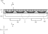
図1は、本発明の第1実施形態のサーマルプリントヘッドの平面図である。図2は、図1のII−II線に沿う断面図である。図3は、図1に示したサーマルプリントヘッドの要部拡大平面図である。図4は、図3のIV−IV線に沿う要部拡大断面図である。 FIG. 1 is a plan view of a thermal print head according to a first embodiment of the present invention. 2 is a cross-sectional view taken along line II-II in FIG. FIG. 3 is an enlarged plan view of a main part of the thermal print head shown in FIG. FIG. 4 is an enlarged cross-sectional view of a main part taken along line IV-IV in FIG.
これらの図に示すサーマルプリントヘッド101は、基材11と、配線基板12と、放熱板13と、蓄熱層2と、電極層3と、抵抗体層4と、絶縁層5と、保護層6(図1では省略)と、駆動IC7と、複数のワイヤ81と、封止樹脂82と、コネクタ83とを備える。サーマルプリントヘッド101は、印刷媒体801に印刷を施すプリンタに組み込まれるものである。このような印刷媒体801としては、たとえばバーコードシートやレシートを作成するための感熱紙が挙げられる。
The
図2に示す放熱板13は、基材11からの熱を放散させるためのものである。放熱板13は、たとえばAlなどの金属よりなる。放熱板13には基材11および配線基板12が取り付けられている。
The
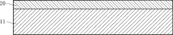
基材11は板状を呈している。本実施形態においては、基材11は半導体材料よりなる。基材11を構成する半導体材料としては、たとえば、Si、SiC、AlN、GaP、GaAs、InP、およびGaNが挙げられる。本実施形態においては、基材11は半導体材料よりなるが、基材11は半導体材料からなっていなくてもよい。たとえば、基材11は、後述するように、セラミックなどの絶縁材料よりなっていてもよい。基材11の厚さはたとえば0.625〜0.720mmである。図1に示すように、基材11は、方向Yに長く延びる平板状である。基材11の幅(基材11の方向Xにおける寸法)は、たとえば、3〜20mmである。基材11の方向Yにおける寸法は、たとえば、10〜300mmである。
The
図4に示すように、基材11は基材表面111を有する。基材表面111は、方向Xと方向Yとに広がる平面状である。基材表面111は、方向Yに沿って長手状に延びる。基材表面111は、基材11の厚さ方向Zの一方(以下、方向Zaと言う。図4では上方)を向く。すなわち、基材表面111は、抵抗体層4の位置する側を向く面である。
As shown in FIG. 4, the
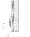
図2および図4に示すように、蓄熱層2は基材11に形成されている。蓄熱層2は、基材11の基材表面111の全体を覆っている。蓄熱層2は、発熱部41(後述)にて発生した熱を蓄えるためのものである。蓄熱層2の厚さは、たとえば、3μm以上である。図4に示すように、蓄熱層2は蓄熱層表面21を有する。蓄熱層表面21は方向Zaを向く。すなわち、蓄熱層表面21は、抵抗体層4の位置する側を向く面である。本実施形態では、蓄熱層表面21は全体にわたって平坦である。蓄熱層表面21が平坦であると、半導体プロセスによって抵抗体層4や絶縁層5を形成しやすい。
As shown in FIGS. 2 and 4, the
図2および図4に示すように、本実施形態では、蓄熱層2は、第1層26と第2層27とを含む。第1層26は、第2層27と基材11との間に位置している。第1層26は、基材11を構成する半導体材料を酸化した材料よりなる層である。たとえば、基材11を構成する半導体材料がSiである場合には、第1層26はSiO2よりなる層である。第2層27は、絶縁材料よりなる層である。第2層27を構成する材料は、特に限定されないが、本実施形態においては、第1層26を構成する材料と同一の材料よりなる。本実施形態とは異なり、蓄熱層2が二層構造ではなく、一層構造であってもよい。また、蓄熱層2を備えない構成であってもよい。
As shown in FIGS. 2 and 4, in the present embodiment, the
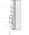
図2〜図4に示す電極層3は基材11に形成されている。図3における電極層3には、理解の便宜上、ハッチを付している。具体的には、電極層3は蓄熱層2に積層されている。また、電極層3は抵抗体層4に積層されている。本実施形態においては、電極層3と蓄熱層2との間に、抵抗体層4が介在している。電極層3は、抵抗体層4に導通している。電極層3は、抵抗体層4に通電するための経路を構成している。電極層3を構成する材料としては、たとえば、Au、Ag、Cu、Cr、Al−Si、および、Tiが挙げられる。本実施形態とは異なり、電極層3は、蓄熱層2と抵抗体層4との間に介在していてもよい。
The
図4に示すように、電極層3は、第1導電部31と第2導電部32とを含む。第1導電部31および第2導電部32は、互いに離間している。
As shown in FIG. 4, the
本実施形態においては、電極層3は、複数の個別電極33(同図には6つ示す)と、一つの共通電極35とを含む。
In the present embodiment, the
複数の個別電極33は、互いに導通していない。そのため、各個別電極33には、サーマルプリントヘッド101の組み込まれたプリンタが使用される際に、個別に、互いに異なる電位が付与されうる。各個別電極33は、屈曲部333と、直行部334と、斜行部335と、ボンディング部336とを有する。直行部334は、電極層3における第1導電部31を構成しており、方向Xに沿って延びる帯状である。直行部334は、抵抗体層4に積層されている。屈曲部333は、直行部334につながり、方向Yおよび方向Xの屈曲形状である。斜行部335は、方向Yおよび方向Xのいずれに対しても傾斜した方向に延びている。ボンディング部336は、ワイヤ81がボンディングされる部分である。
The plurality of
共通電極35は、サーマルプリントヘッド101の組み込まれたプリンタが使用される際に複数の個別電極33に対して電気的に逆極性となる部位である。共通電極35は、複数の共通電極帯状部351と、横行部352と、を有する。各共通電極帯状部351は、方向Xに延びる帯状である。共通電極35において、複数の共通電極帯状部351は、電極層3における第2導電部32を構成しており、第1導電部31に対して方向Yに離間している。共通電極帯状部351は、抵抗体層4に積層されている。複数の共通電極帯状部351、および複数の個別電極帯状部331は、方向Yに沿って配列されている。横行部352は、方向Yに長く延びる帯状であり、複数の共通電極帯状部351がつながっている。
The
抵抗体層4は基材11に形成されている。本実施形態では、抵抗体層4は、蓄熱層2に直接形成されている。本実施形態においては、抵抗体層4は、複数の矩形状の部分を有する。抵抗体層4は、電極層3からの電流が流れた部分が発熱する。このように発熱することによって印字ドットが形成される。抵抗体層4は、電極層3を構成する材料よりも抵抗率が高い材料よりなる。抵抗体層4を構成する材料としては、たとえば、ポリシリコン、TaSiO2、および、TiONが挙げられる。本実施形態においては、抵抗体層4には、抵抗値の調整のため、イオン(たとえば、ホウ素)がドーピングされている。抵抗体層4の厚さは、たとえば、0.2μm〜1μmである。
The
図4に示すように、抵抗体層4は、第1端面416と、第2端面417とを有する。
As shown in FIG. 4, the
第1端面416は、第2導電部32(共通電極帯状部351)の位置する側とは反対側(すなわち、図4の右方向)を向いている。第2端面417は、第1導電部31(個別電極帯状部331)の位置する側とは反対側(すなわち、図4の左方向)を向いている。
The
抵抗体層4は、サーマルプリントヘッド101の使用時に発熱する発熱部41を含む。発熱部41は、基材11の厚さ方向視において、第1導電部31および第2導電部32に重なっている。各発熱部41は蓄熱層2に積層されている。複数の発熱部41は、方向Yに沿って配列されている。
The
発熱部41は、第1当接部411および第2当接部412を含んでいる。第1当接部411は、電極層3における第1導電部31に当接している。第2当接部412は、電極層3における第2導電部32に当接している。
The
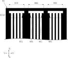
複数の発熱部41は、縮小部419を有するものを含んでいる。縮小部419は、方向Yにおける寸法が小とされた部位であり、第1導電部31および第2導電部32に対して方向Yに凹んでいる。本実施形態においては、縮小部419を有する2つの発熱部41が、縮小部419を有さない一定数の発熱部41を挟んで配置されている。なお、図示された例においては、縮小部419を有する2つの発熱部41が、縮小部419を有さない2つの発熱部41を挟んで配置されている。また、本実施形態においては、複数の発熱部41は、互いに隣り合う2つの発熱部41であって、互いに対面する側に各々縮小部419が形成されているものを含む。すなわち、隣り合う発熱部41のそれぞれに形成された縮小部419が、互いに対面するように配置されている。
The plurality of
絶縁層5は、発熱部41および電極層3の間に介在している部分を有する。絶縁層5を構成する材料としては、たとえば、SiO2、および、SiAlO2が挙げられる。絶縁層5は、第1介在部51と、第2介在部52と、中間部53とを含む。第1介在部51は、第1導電部31および発熱部41の間に介在している部位である。第2介在部52は、第2導電部32および発熱部41の間に介在している。中間部53は、基材11の厚さ方向Z視において、第1介在部51と第2介在部52とに挟まれている。中間部53は、第1介在部51および第2介在部52につながっている。
The insulating
本実施形態において、第1介在部51には、少なくとも1以上の第1開口511が形成されている。第1開口511は、たとえば円形状である。第1開口511の個数は、複数でも1つであってもよい。第1開口511と重なる位置に、上述の発熱部41における第1当接部411が位置している。図6に示すように、本実施形態においては更に、第1開口511内に、第1導電部31の一部が形成されている。
In the present embodiment, at least one or more
本実施形態において、第2介在部52には、少なくとも1以上の第2開口521が形成されている。第2開口521は、たとえば円形状である。第2開口521は、複数でも1つであってもよい。第2開口521と重なる位置に、上述の発熱部41における第2当接部412が位置している。図6に示すように、本実施形態においては更に、第2開口521内に、第2導電部32の一部が形成されている。
In the present embodiment, at least one or more
本実施形態においては、絶縁層5は、部分581,582を含む。部分581は、第1介在部51につながり且つ第1端面416を覆う部分である。部分582は、第2介在部52につながり且つ第2端面417を覆う部分である。部分581,582はそれぞれ、蓄熱層2に直接接している。すなわち、絶縁層5に直接接する部分を、蓄熱層2が有している。本実施形態とは異なり、絶縁層5が部分581,582を含んでいなくてもよい。
In the present embodiment, the insulating
保護層6は、電極層3と抵抗体層4と絶縁層5とを覆っており、電極層3と抵抗体層4と絶縁層5とを保護するためのものである。保護層6は、絶縁材料よりなる。保護層6を構成する絶縁材料としては、たとえば、SiNおよびSiO2が挙げられる。本実施形態においては、保護層6は、電極層3および絶縁層5に直接接している。
The
保護層6には、複数の貫通窓61(図2には1つ示す)が形成されている。各貫通窓61からは、ボンディング部336が露出している。
A plurality of through windows 61 (one shown in FIG. 2) are formed in the
図2に示す配線基板12は、たとえば、プリント配線基板である。配線基板12は、基材層と図示しない配線層とが積層された構造を有する。基材層は、たとえばガラスエポキシ樹脂よりなる。配線層は、たとえばCuよりなる。
The
図2、図3に示す駆動IC7は、各個別電極33にそれぞれ電位を付与し、各発熱部41に流す電流を制御するものである。各個別電極33にそれぞれ電位が付与されることにより、共通電極35と各個別電極33との間に電圧が印加され、各発熱部41に選択的に電流が流れる。駆動IC7は、配線基板12に搭載されている。図3に示すように、駆動IC7は、複数のパッド71を含む。複数のパッド71は、たとえば、2列に形成されている。
The driving
図2、図3に示す複数のワイヤ81は、たとえば、Auなどの導体よりなる。複数のワイヤ81のうちワイヤ811はそれぞれ、駆動IC7にボンディングされ、且つ、電極層3にボンディングされている。より具体的には、各ワイヤ811は、駆動IC7におけるパッド71にボンディングされ、且つ、ボンディング部336にボンディングされている。これにより、駆動IC7と各個別電極33とが導通している。複数のワイヤ81のうちワイヤ812は、それぞれ、駆動IC7におけるパッド71にボンディングされ、且つ、配線基板12における配線層にボンディングされている。これにより、当該配線層を介して、駆動IC7とコネクタ83とが導通している。
The plurality of
図2に示す封止樹脂82は、たとえば、黒色の樹脂よりなる。封止樹脂82は、駆動IC7、複数のワイヤ81、および、保護層6を覆っており、駆動IC7および複数のワイヤ81を保護している。封止樹脂82は保護層6に直接接する。コネクタ83は、配線基板12に固定されている。コネクタ83は、サーマルプリントヘッド101の外部からサーマルプリントヘッド101へ電力を供給し、駆動IC7を制御するためのものである。
The sealing
次に、サーマルプリントヘッド101の使用方法の一例について簡単に説明する。
Next, an example of how to use the
サーマルプリントヘッド101は、プリンタに組み込まれた状態で使用される。図2に示したように、当該プリンタ内において、サーマルプリントヘッド101の各発熱部41はプラテンローラ802に対向している。当該プリンタの使用時には、プラテンローラ802が回転することにより、印刷媒体801が、方向Xに沿ってプラテンローラ802と各発熱部41との間に一定速度で送給される。印刷媒体801は、プラテンローラ802によって保護層6のうち各発熱部41を覆う部分に押しあてられる。一方、図3に示した各個別電極33には、駆動IC7によって選択的に電位が付与される。これにより、共通電極35と複数の個別電極33の各々との間に電圧が印加される。そして、複数の発熱部41には選択的に電流が流れ、熱が発生する。そして、各発熱部41にて発生した熱は、保護層6を介して印刷媒体801に伝わる。そして、印刷媒体801上の方向Yに線状に延びる第1ライン領域に、複数のドットが印刷される。また、各発熱部41にて発生した熱は、蓄熱層2にも伝わり、蓄熱層2にて蓄えられる。
The
更に、プラテンローラ802が回転することにより、印刷媒体801が、方向Xに沿って一定速度で引き続き送給される。そして、上述の第1ライン領域への印刷と同様に、印刷媒体801上の方向Yに線状に延びる、第1ライン領域に隣接する第2ライン領域への印刷が行われる。第2ライン領域への印刷の際、印刷媒体801には、各発熱部41にて発生した熱に加え、第1ライン領域への印刷時に蓄熱層2にて蓄えられた熱が伝わる。このようにして、第2ライン領域への印刷が行われる。以上のように、印刷媒体801上の方向Yに線状に延びるライン領域ごとに、複数のドットを印刷することにより、印刷媒体801への印刷が行われる。
Further, the
次に、サーマルプリントヘッド101の製造方法の一例について簡単に説明する。本実施形態においてサーマルプリントヘッド101を製造するには、半導体プロセスを用いる。
Next, an example of a method for manufacturing the
まず、図5に示すように、半導体基板19を用意する。本実施形態において半導体基板19はSiよりなる。次に、図6に示すように、半導体基板19の表面を熱酸化する。これにより、基材11と、基材11に積層された第1層26とが形成される。本実施形態においては、第1層26は、SiO2よりなる。次に、図7に示すように、CVDもしくはスパッタによって、第1層26上に第2層27を形成する。これにより、基材11に積層された蓄熱層2が形成される。図示することは省略するが、基材11の裏面にもSiO2
層が形成される。なお、本実施形態とは異なり、半導体基板19の表面を熱酸化する必要は必ずしもなく、CVDもしくはスパッタによって、直接、蓄熱層2を形成してもよい。
First, as shown in FIG. 5, a
A layer is formed. Unlike the present embodiment, it is not always necessary to thermally oxidize the surface of the
次に、図8に示すように、抵抗体材料層4’を形成する。抵抗体材料層4’の形成は、たとえば、CVDもしくはスパッタにより行う。抵抗体材料層4’は、基材11の表面の全面に形成する。次に、図9、図10に示すように、抵抗体材料層4’をエッチングすることにより、抵抗体材料層4’’を形成する。抵抗体材料層4’のエッチングは、フォトリソグラフィーにより行う。図10に示すように、本実施形態では、抵抗体材料層4’’は、一方向に沿って帯状に延びる形状である。次に、抵抗体層4が所望の抵抗値になるように、抵抗体材料層4’’にイオンを打ち込む(図示略)。
Next, as shown in FIG. 8, a resistor material layer 4 'is formed. The resistor material layer 4 'is formed by, for example, CVD or sputtering. The
次に、図11に示すように、絶縁材料層5’を形成する。絶縁材料層5’の形成は、たとえば、CVDもしくはスパッタにより行う。次に、図12、図13に示すように、絶縁材料層5’をエッチングすることにより、上述の絶縁層5を形成する。絶縁材料層5’をエッチングする当該工程を経ることにより、上述の第1開口511および第2開口521が形成される。
Next, as shown in FIG. 11, an insulating material layer 5 'is formed. The insulating material layer 5 'is formed by, for example, CVD or sputtering. Next, as shown in FIGS. 12 and 13, the insulating
次に、図14、図15に示すように、電極材料層3’を形成する。電極材料層3’の形成は、たとえば、スパッタもしくはCVDにより行う。次に、図16に示すように、電極材料層3’のうち方向Yに長く延びる領域をエッチングによって除去する。これにより、絶縁層5の一部が、電極材料層3’から露出する。
Next, as shown in FIGS. 14 and 15, an electrode material layer 3 'is formed. The electrode material layer 3 'is formed by sputtering or CVD, for example. Next, as shown in FIG. 16, a region extending in the direction Y in the electrode material layer 3 'is removed by etching. Thereby, a part of the insulating
次に、図17および図18に示すように、蓄熱層2、電極材料層3’、抵抗体材料層4’および絶縁層5を覆うように、レジスト材料層60’を形成する。レジスト材料層60’の形成は、たとえば感光性樹脂材料を含む液体またはペーストを塗布することによって行う。
Next, as shown in FIGS. 17 and 18, a resist
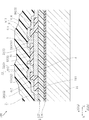
次に、図19に示すフォトリソグラフィマスク85を用いて縮小投影露光を行う。フォトリソグラフィマスク85は、縮小投影露光において、レジスト材料層60’に部分的且つ選択的に光を当てるためのものである。本実施形態においては、レジスト材料層60’のうち露光された部分が残存する、いわゆるネガ型である場合を例に説明するが、これとは異なり、レジスト材料層60’がいわゆるポジ型である場合であっても、本発明は適用可能である。
Next, reduced projection exposure is performed using a
フォトリソグラフィマスク85は、電極層3および抵抗体層4として残存させるべき部分の形状が除去された板状部材である。本実施形態においては、フォトリソグラフィマスク85を用いた縮小投影露光を行うため、フォトリソグラフィマスク85の各部のサイズは、電極層3および抵抗体層4の対応する各部のサイズよりも大である。
The
本実施形態においては、フォトリソグラフィマスク85は、反復露光部860、第1端部870、および第2端部880を有する。反復露光部860は、電極層3および抵抗体層4の大部分を形成するための縮小投影露光に用いられる。本実施形態においては、は、反復露光部860は、電極層3および抵抗体層4の一部に相当する。第1端部870は、反復露光部860によって形成される電極層3および抵抗体層4の部分に対して、方向Y一端側に隣接する部分を形成するための部位である。第2端部880は、反復露光部860によって形成される電極層3および抵抗体層4の部分に対して、方向Y他端側に隣接する部分を形成するための部位である。
In the present embodiment, the
本実施形態においては、反復露光部860は、第1導電部31、第2導電部32および発熱部41を形成するための部分を有しており、さらに個別電極33および共通電極35を形成するための部位を有する。第1端部870は、第1導電部31、第2導電部32および発熱部41を形成するための部分を有しており、さらに個別電極33および共通電極35を形成するための部位を有する。第2端部880は、第1導電部31、第2導電部32および発熱部41を形成するための部分を有しており、さらに個別電極33および共通電極35を形成するための部位を有する。
In the present embodiment, the repeated
反復露光部860は、2つの縮小部861を有している。縮小部861は、方向Y端部領域において方向Y寸法が小とされた部位である。反復露光部860においては、方向Y両端に2つの縮小部861が設けられている。また、縮小部861は、方向Xにおいて、発熱部41を露光する部分と重なっている。
The repeated
第1端部870は、第1縮小部871を有している。第1縮小部871は、方向Y端部領域(図中右端領域)において方向Y寸法が小とされた部位である。第1縮小部871は、方向Xにおいて、発熱部41を露光する部分と重なっている。
The
第2端部880は、第2縮小部881を有している。第2縮小部881は、方向Y端部領域(図中左端領域)において方向Y寸法が小とされた部位である。第2縮小部881は、方向Xにおいて、発熱部41を露光する部分と重なっている。
The
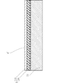
図20〜図24は、露光工程を示している。これらの図においては理解の便宜上、フォトリソグラフィマスク85と基材11およびレジスト材料層60'とを模式的に示している。
20 to 24 show the exposure process. In these drawings, for convenience of understanding, the
図20は、フォトリソグラフィマスク85の第1端部870を用いた縮小投影露光を示している。図中の一点鎖線は、集光された光を模式的に示す。フォトリソグラフィマスク85のうち第1端部870以外の部分を遮光した状態で、第1端部870を透してレジスト材料層60’に向けて集光される光をレジスト材料層60’に集光投影露光する。図中においては、レジスト材料層60’のうち露光された部分に、相対的に細かいハッチングが施されている。これにより、フォトリソグラフィマスク85の第1端部870が、集光度合いに応じて縮小され、レジスト材料層60’に露光される。レジスト材料層60’がネガ型であるため、この露光部分は、除去液などに対して残存する部位となる。
FIG. 20 shows reduced projection exposure using the
次いで、図21に示すように、フォトリソグラフィマスク85を基材11に対して方向Yに相対的に移動させる。この相対的な移動は、フォトリソグラフィマスク85を動かすことによって実現してもよいし、基材11を動かすことによって実現してもよい。この移動を経て、フォトリソグラフィマスク85の反復露光部860以外の部分を遮光した状態で、反復露光部860を透してレジスト材料層60’に向けて集光される光をレジスト材料層60’に集光投影露光する。この際の露光位置は、図20に示した第1端部870によって露光された部分と隣接している。
Next, as shown in FIG. 21, the
次いで、図22に示すように、フォトリソグラフィマスク85を基材11に対して方向Yに相対的に移動させる。この移動を経て、フォトリソグラフィマスク85の反復露光部860以外の部分を遮光した状態で、反復露光部860を透してレジスト材料層60’に向けて集光される光をレジスト材料層60’に集光投影露光する。この際の露光位置は、図21に示した反復露光部860によって露光された部分と隣接している。
Next, as shown in FIG. 22, the
次いで、図23に示すように、フォトリソグラフィマスク85を基材11に対して方向Yに相対的に移動させる。この移動を経て、フォトリソグラフィマスク85の反復露光部860以外の部分を遮光した状態で、反復露光部860を透してレジスト材料層60’に向けて集光される光をレジスト材料層60’に集光投影露光する。この際の露光位置は、図22に示した反復露光部860によって露光された部分と隣接している。この反復露光部860を用いた縮小投影露光とフォトリソグラフィマスク85および基材11の相対的な移動とを繰り返す。繰り返し回数は、サーマルプリントヘッド101を構成するのに必要とされる電極層3および抵抗体層4を構築可能な回数が選択される。
Next, as shown in FIG. 23, the
次いで、図24に示すように、フォトリソグラフィマスク85を基材11に対して方向Yに相対的に移動させる。この移動を経て、フォトリソグラフィマスク85の第2端部880以外の部分を遮光した状態で、第2端部880を透してレジスト材料層60’に向けて集光される光をレジスト材料層60’に集光投影露光する。この際の露光位置は、反復露光部860によって露光された部分の図中右端と隣接している。
Next, as shown in FIG. 24, the
このような複数回の縮小投影露光を終えた後に、未露光のレジスト材料層60’を除去し、露光されたレジスト材料層60’を残存させうる除去液を用いてレジスト材料層60’を部分的に除去する。これにより、図25に示すようにレジスト層60が得られる。レジスト層60は、個別電極33、共通電極35および発熱部41となるべき部分を覆う形状とされている。また、本実施形態においては、レジスト層60は、複数の縮小部69を有している。複数の縮小部69は、図19に示したように、フォトリソグラフィマスク85に縮小部861,871,881が形成されていたことから、レジスト材料層60’のうち露光された領域が方向Yに部分的に縮小された部位を有することに起因して形成されている。このレジスト層60をマスクとして用いたエッチングによって電極材料層3’をエッチングすることにより、電極層3が得られる。また、抵抗体材料層4’’をエッチングすることにより、抵抗体層4が得られる。なお、電極材料層3’および抵抗体材料層4’’のエッチングは、一括して行ってもよいし、各々を選択的に除去可能なエッチング液を使い分けることにより、別々のタイミングで行ってもよい。この後は、レジスト層60を除去することにより、図26に示す電極層3および抵抗体層4が得られる。また、複数の縮小部69に対応する部位に、複数の縮小部419が形成される。
After such multiple times of reduced projection exposure, the unexposed resist
次に、図27に示すように、保護材料層6’を形成する。保護材料層6’の形成は、たとえば、CVDにより行う。次に、図28に示すように、保護材料層6’をエッチングすることにより、複数の貫通窓61を形成する。保護材料層6’のエッチングは、フォトリソグラフィーにより行う。
Next, as shown in FIG. 27, a protective material layer 6 'is formed. The protective material layer 6 'is formed by, for example, CVD. Next, as shown in FIG. 28, the plurality of through
次に、図示は省略するが、基材11の裏面を研磨することにより、基材11の厚みを低減させる。次に、抵抗体層4の抵抗値の測定、および、基材11のダイシングを行ったのち、ダイシング後の製品と、配線基板12とを放熱板13に配置する。次に、図2に示した、駆動IC7を配線基板12に搭載し、ワイヤ81を所望の箇所にボンディングし、封止樹脂82を形成する。これらの工程を経るなどして、図2に示したサーマルプリントヘッド101が製造される。
Next, although illustration is omitted, the thickness of the
以上の工程を経て得られたサーマルプリントヘッド101においては、複数の発熱部41の方向Yピッチが、たとえば43.2μmである。また、隣り合う発熱部41同士の隙間は、たとえば0.1μm程度に設定可能である。
In the
次に、本実施形態の作用効果について説明する。 Next, the effect of this embodiment is demonstrated.
本実施形態においては、フォトリソグラフィマスク85を用いた縮小投影露光によってレジスト材料層60’を露光する。これにより、フォトリソグラフィマスク85に形成されたパターンが、正確な形状を維持しつつ集光度合いに応じた縮小を受けて、レジスト層60に写像される。このため、フォトリソグラフィマスク85の製作精度を過度に精密にすることなく、レジスト層60を微細に形成することが可能である。したがって、サーマルプリントヘッド101の印刷の高精細化を図ることが可能であり、印刷品位を向上させることができる。
In the present embodiment, the resist
また、フォトリソグラフィマスク85は、反復露光部860、第1端部870および第2端部880を有している。電極層3および抵抗体層4のうち方向Y両端付近を除く部分は、一定の部分パターンが繰り返されたパターンとなっている。この部分を、反復露光部860を用いた縮小投影露光を繰り返して形成することにより、フォトリソグラフィマスク85が不当に大型となってしまうことを防止することができる。また、反復露光部860を複数回用いることにより、電極層3および抵抗体層4の形状が方向Yの一端側、中央側および他端側などにおいて不揃いとなってしまうことを回避することができる。第1端部870および第2端部880を有する事により、電極層3および抵抗体層4のうち方向Y端部において、中央寄りの定常部分とはことなるパターンとすることも可能である。
The
縮小部861、第1縮小部871および第2縮小部881を有することにより、反復露光部860、第1端部870および第2端部880によって露光させたい領域に隣接する領域に、意図せず光を当ててしまうことを防止することができる。これは、いわゆる光の回折を考慮した方策である。また、縮小部861、第1縮小部871および第2縮小部881を、方向Xにおいて発熱部41と重なるものとすることにより、印刷品位の向上に大きく影響する複数の発熱部41をより正確に形成することができる。複数の発熱部41が、縮小部419を有するものを含むことにより、隣接する発熱部41が意図せず接触してしまうなどの事態を適切に回避することができる。
By including the
以下の説明では、上記と同一もしくは類似の構成については上記と同一の符号を付し、説明を適宜省略する。 In the following description, the same or similar components as those described above will be denoted by the same reference numerals as those described above, and description thereof will be omitted as appropriate.
<第2実施形態>
図29〜個別電極33を用いて、本発明の第2実施形態について説明する。
<Second Embodiment>
A second embodiment of the present invention will be described with reference to FIGS.
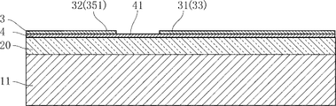
図29に示す基材11は、セラミックスよりなり、たとえばAl2O3よりなる。基材11上に、グレーズ層20を形成する。グレーズ層20は、電極層3および抵抗体層4を形成しうる平坦度を担保するためのものであり、たとえばガラスよりなる。
次に、図30に示すように、グレーズ層20上に抵抗体材料層4’を形成する。抵抗体材料層4’は、たとえばTaSiO2またはTaNよりなる。抵抗体材料層4’の形成は、たとえばCVDまたはスパッタにより行う。抵抗体材料層4’は、グレーズ層20の全面を覆っている。
Next, as shown in FIG. 30, the
次に、図31に示すように、電極材料層3’を形成する。電極材料層3’は、たとえばAl、Cu、および、Auの少なくともいずれかよりなる。電極材料層3’の形成は、たとえばCVDまたはスパッタにより行う。電極材料層3’は、抵抗体材料層4’全体を覆うように形成されてもよいし、抵抗体材料層4’のうち発熱部41となるべき部分を露出させるように形成してもよい。
Next, as shown in FIG. 31, an electrode material layer 3 'is formed. The
次いで、図17および図18を参照して説明したレジスト材料層60'を形成する。続いて、図19に示すフォトリソグラフィマスク85を用いた縮小投影露光を行う。この縮小投影露光の手順は、図20〜図24を参照して説明した手順と同様である。この露光工程の後にレジスト材料層60'を部分的且つ選択的に除去することにより、レジスト層60が得られる。そして、レジスト層60をマスクとして用いたエッチングにより、図32に示すように、電極層3および抵抗体層4が得られる。この後は、保護層6の形成等を適宜行うことにより、図33に示すサーマルプリントヘッド102が得られる。サーマルプリントヘッド102は、いわゆる薄膜型のサーマルプリントヘッドである。
Next, the resist
このような実施形態によっても、サーマルプリントヘッド102の印刷の高精細化を図ることができる。
According to such an embodiment as well, high definition printing of the
本発明は、上述した実施形態に限定されるものではない。本発明の具体的な構成は、種々に設計変更自在である。 The present invention is not limited to the embodiment described above. The specific configuration of the present invention can be modified in various ways.
101 サーマルプリントヘッド
102 サーマルプリントヘッド
11 基材
111 基材表面
12 配線基板
13 放熱板
19 半導体基板
2 蓄熱層
21 蓄熱層表面
26 第1層
27 第2層
20 グレーズ層
3 電極層
3’ 電極材料層
31 第1導電部
32 第2導電部
33 個別電極
331 個別電極帯状部
333 屈曲部
334 直行部
335 斜行部
336 ボンディング部
35 共通電極
351 共通電極帯状部
352 横行部
4 抵抗体層
4’ 抵抗体材料層
4’’ 抵抗体材料層
41 発熱部
411 第1当接部
412 第2当接部
416 第1端面
417 第2端面
419 縮小部
5 絶縁層
5’ 絶縁材料層
51 第1介在部
511 第1開口
52 第2介在部
521 第2開口
53 中間部
581 部分
582 部分
60 レジスト層
60’ レジスト材料層
69 縮小部
6 保護層
6’ 保護材料層
61 貫通窓
7 駆動IC
71 パッド
81 ワイヤ
811 ワイヤ
812 ワイヤ
82 封止樹脂
83 コネクタ
801 印刷媒体
802 プラテンローラ
85 フォトリソグラフィマスク
860 反復露光部
861 縮小部
870 第1端部
871 第1縮小部
880 第2端部
881 第2縮小部
DESCRIPTION OF
71
Claims (34)
前記基材に形成された抵抗体層と、
前記基材に形成され且つ前記抵抗体層と導通する電極層と、
絶縁層と、を備え、
前記電極層は、互いに離間する第1導電部および第2導電部を含み、
前記抵抗体層は、前記基材の厚さ方向視において、前記第1導電部および前記第2導電部に重なる部分を有する発熱部を含む、サーマルプリントヘッドの製造方法であって、
前記基材に前記抵抗体層となる抵抗体材料層および前記電極層となる電極材料層を形成する工程と、
前記抵抗体材料層および前記電極材料層を覆うレジスト材料層を形成する工程と、
フォトリソグラフィマスクに形成されたパターンを前記レジスト材料層に縮小投影露光する露光工程と、
前記レジスト材料層のうち前記露光工程の後に除去容易となっている部分を除去することによりレジスト層を形成する工程と、
前記レジスト層を用いたエッチングによって前記抵抗体材料層および前記電極材料層の少なくともいずれかをパターニングする工程と、
を備え、
前記露光工程においては、前記フォトリソグラフィマスクの反復露光部を用いて縮小投影露光する処理と、前記フォトリソグラフィマスクの前記反復露光部を前記基材の主走査方向に沿って相対的に移動させる処理と、を繰り返し、
前記反復露光部は、複数の前記発熱部に相当する部位を含み、
前記反復露光部の光透過部分のうち前記主走査方向端に位置する部位は、前記主走査方向寸法が小とされた縮小部を有する、サーマルプリントヘッドの製造方法。 A substrate;
A resistor layer formed on the substrate;
An electrode layer formed on the substrate and electrically connected to the resistor layer;
An insulating layer;
The electrode layer includes a first conductive portion and a second conductive portion that are separated from each other,
The resistor layer includes a heat generating part having a portion overlapping the first conductive part and the second conductive part in a thickness direction view of the base material,
Forming a resistor material layer to be the resistor layer and an electrode material layer to be the electrode layer on the substrate;
Forming a resist material layer covering the resistor material layer and the electrode material layer;
An exposure process for reducing and projecting a pattern formed on a photolithography mask onto the resist material layer; and
Forming a resist layer by removing a portion of the resist material layer that is easily removed after the exposure step;
Patterning at least one of the resistor material layer and the electrode material layer by etching using the resist layer;
With
In the exposure step, a reduction projection exposure process using a repetitive exposure part of the photolithography mask, and a process of relatively moving the repetitive exposure part of the photolithography mask along the main scanning direction of the substrate And repeat
The repeated exposure portion includes a plurality of portions corresponding to the heat generating portions,
Site located in the main scanning direction end of the light transmitting portion of the repetitive exposure unit, the main that the scanning direction dimensions have a reduced portion which is small, manufacturing method for a thermal print head.
ルプリントヘッドの製造方法。 27. The method of manufacturing a thermal print head according to claim 26 , wherein the resistor material layer is made of TaSiO 2 or TaN.
前記基材に形成された抵抗体層と、
前記基材に形成され且つ前記抵抗体層と導通する電極層と、
絶縁層と、を備え、
前記電極層は、互いに離間する第1導電部および第2導電部を含み、
前記抵抗体層は、各々が前記基材の厚さ方向視において、前記第1導電部および前記第2導電部に重なる部分を有する、前記基材の主走査方向に配列された複数の発熱部を含む、サーマルプリントヘッドであって、
前記複数の発熱部の少なくともいずれかは、該発熱部が重なる前記第1導電部および前記第2導電部に対して前記主走査方向において内方に凹む縮小部を有し、
前記基材に形成された抵抗体材料層および電極材料層を覆うレジスト材料層に対するフォトリソグラフィマスクのパターンの縮小投影露光と、前記レジスト材料層のうち前記縮小投影露光により除去容易となっている部分を除去することによるレジスト層の形成と、前記レジスト層を用いたエッチングとによって、前記抵抗体材料層がパターニングされて前記抵抗体層が得られること、および、前記電極材料層がパターニングされて前記電極層が得られること、の少なくともいずれかが行われ、
前記縮小投影露光は、前記フォトリソグラフィマスクの反復露光部を用いて縮小投影露光する処理と、前記フォトリソグラフィマスクの前記反復露光部を前記主走査方向に沿って相対的に移動させる処理と、を繰り返すことによって行われ、
前記反復露光部は、複数の前記発熱部に相当する部位を含み、
前記反復露光部の光透過部分のうち前記主走査方向端に位置する部位は、前記主走査方向寸法が小とされ前記縮小部に対応する、サーマルプリントヘッド。 A substrate;
A resistor layer formed on the substrate;
An electrode layer formed on the substrate and electrically connected to the resistor layer;
An insulating layer;
The electrode layer includes a first conductive portion and a second conductive portion that are separated from each other,
The resistor layer has a plurality of heating portions arranged in the main scanning direction of the base material, each having a portion overlapping the first conductive portion and the second conductive portion in the thickness direction of the base material Including a thermal print head,
At least one of the plurality of heat-generating unit may have a reduced portion concaved inwardly in the main scanning direction with respect to the first conductive portion and the second conductive part heat generating portion overlap,
Reduced projection exposure of the pattern of the photolithography mask to the resist material layer covering the resistor material layer and the electrode material layer formed on the base material, and a portion of the resist material layer that is easily removed by the reduced projection exposure The resistor material layer is patterned to form the resistor layer by forming a resist layer by removing the resist layer and etching using the resist layer, and the electrode material layer is patterned to form the resistor layer. At least one of obtaining an electrode layer is performed,
The reduced projection exposure includes a process of performing reduced projection exposure using a repeated exposure unit of the photolithography mask, and a process of relatively moving the repeated exposure unit of the photolithography mask along the main scanning direction. Done by repeating,
The repeated exposure portion includes a plurality of portions corresponding to the heat generating portions,
A portion of the light transmissive portion of the repeated exposure portion located at the end in the main scanning direction has a small size in the main scanning direction and corresponds to the reduction portion .
Priority Applications (1)
| Application Number | Priority Date | Filing Date | Title |
|---|---|---|---|
| JP2015124784A JP6557066B2 (en) | 2015-06-22 | 2015-06-22 | Thermal print head manufacturing method and thermal print head |
Applications Claiming Priority (1)
| Application Number | Priority Date | Filing Date | Title |
|---|---|---|---|
| JP2015124784A JP6557066B2 (en) | 2015-06-22 | 2015-06-22 | Thermal print head manufacturing method and thermal print head |
Publications (2)
| Publication Number | Publication Date |
|---|---|
| JP2017007203A JP2017007203A (en) | 2017-01-12 |
| JP6557066B2 true JP6557066B2 (en) | 2019-08-07 |
Family
ID=57762667
Family Applications (1)
| Application Number | Title | Priority Date | Filing Date |
|---|---|---|---|
| JP2015124784A Expired - Fee Related JP6557066B2 (en) | 2015-06-22 | 2015-06-22 | Thermal print head manufacturing method and thermal print head |
Country Status (1)
| Country | Link |
|---|---|
| JP (1) | JP6557066B2 (en) |
Families Citing this family (2)
| Publication number | Priority date | Publication date | Assignee | Title |
|---|---|---|---|---|
| JP2018176549A (en) * | 2017-04-13 | 2018-11-15 | ローム株式会社 | Thermal print head and method of manufacturing thermal print head |
| JP2021011020A (en) * | 2019-07-03 | 2021-02-04 | ローム株式会社 | Thermal print head and its manufacturing method |
Family Cites Families (7)
| Publication number | Priority date | Publication date | Assignee | Title |
|---|---|---|---|---|
| US3955068A (en) * | 1974-09-27 | 1976-05-04 | Rockwell International Corporation | Flexible conductor-resistor composite |
| JPH01152460A (en) * | 1987-12-09 | 1989-06-14 | Oki Electric Ind Co Ltd | Exposing method for photolithography process |
| JPH01267513A (en) * | 1988-04-19 | 1989-10-25 | Asahi Optical Co Ltd | Imaging lens |
| JP2775869B2 (en) * | 1989-07-12 | 1998-07-16 | 富士ゼロックス株式会社 | Wiring pattern patterning method in image sensor manufacturing |
| US5705299A (en) * | 1992-12-16 | 1998-01-06 | Texas Instruments Incorporated | Large die photolithography |
| JP2004219587A (en) * | 2003-01-10 | 2004-08-05 | Dainippon Printing Co Ltd | Method of creating photomask data having optical proximity correction pattern, and photomask having optical proximity correction pattern |
| JP6178669B2 (en) * | 2012-08-29 | 2017-08-09 | ローム株式会社 | Thermal print head and thermal printer |
-
2015
- 2015-06-22 JP JP2015124784A patent/JP6557066B2/en not_active Expired - Fee Related
Also Published As
| Publication number | Publication date |
|---|---|
| JP2017007203A (en) | 2017-01-12 |
Similar Documents
| Publication | Publication Date | Title |
|---|---|---|
| JP6371529B2 (en) | Thermal print head, thermal printer | |
| CN102555515A (en) | Thermal print head and method of manufacturing the same | |
| JP6557066B2 (en) | Thermal print head manufacturing method and thermal print head | |
| JP6209019B2 (en) | Thermal print head, thermal printer | |
| JP5972654B2 (en) | Thermal print head and method of manufacturing thermal print head | |
| JP7269802B2 (en) | Thermal print head and manufacturing method thereof | |
| JP7001388B2 (en) | Manufacturing method of thermal print head and thermal print head | |
| JP6654628B2 (en) | Thermal printhead and method of manufacturing thermal printhead | |
| JP2013202796A (en) | Thermal print head | |
| JP4448433B2 (en) | Manufacturing method of thermal head | |
| JP2016215389A (en) | Thermal print head | |
| JP6219076B2 (en) | Thermal print head, thermal printer | |
| JP7219634B2 (en) | thermal print head | |
| JP6341723B2 (en) | Thermal print head and thermal printer | |
| JP5820107B2 (en) | Thermal print head and manufacturing method thereof | |
| JP7271248B2 (en) | thermal print head | |
| JP7545854B2 (en) | Thermal printhead and method for manufacturing the same | |
| JP2009066854A (en) | Thermal print head and method for manufacturing the same | |
| JP4969600B2 (en) | Thermal print head | |
| JP5260038B2 (en) | Thermal print head and manufacturing method thereof | |
| WO2015159819A1 (en) | Thermal print head and thermal printer | |
| CN119369835A (en) | Thermal print head | |
| JP6422225B2 (en) | Thermal head | |
| JP2014188980A (en) | Thermal print head | |
| JP2023165458A (en) | Thermal print head and thermal printer |
Legal Events
| Date | Code | Title | Description |
|---|---|---|---|
| A621 | Written request for application examination |
Free format text: JAPANESE INTERMEDIATE CODE: A621 Effective date: 20180523 |
|
| A977 | Report on retrieval |
Free format text: JAPANESE INTERMEDIATE CODE: A971007 Effective date: 20190410 |
|
| A131 | Notification of reasons for refusal |
Free format text: JAPANESE INTERMEDIATE CODE: A131 Effective date: 20190416 |
|
| A521 | Request for written amendment filed |
Free format text: JAPANESE INTERMEDIATE CODE: A523 Effective date: 20190614 |
|
| TRDD | Decision of grant or rejection written | ||
| A01 | Written decision to grant a patent or to grant a registration (utility model) |
Free format text: JAPANESE INTERMEDIATE CODE: A01 Effective date: 20190625 |
|
| A61 | First payment of annual fees (during grant procedure) |
Free format text: JAPANESE INTERMEDIATE CODE: A61 Effective date: 20190711 |
|
| R150 | Certificate of patent or registration of utility model |
Ref document number: 6557066 Country of ref document: JP Free format text: JAPANESE INTERMEDIATE CODE: R150 |
|
| R250 | Receipt of annual fees |
Free format text: JAPANESE INTERMEDIATE CODE: R250 |
|
| R250 | Receipt of annual fees |
Free format text: JAPANESE INTERMEDIATE CODE: R250 |
|
| LAPS | Cancellation because of no payment of annual fees |