JP7269802B2 - Thermal print head and manufacturing method thereof - Google Patents
Thermal print head and manufacturing method thereof Download PDFInfo
- Publication number
- JP7269802B2 JP7269802B2 JP2019117056A JP2019117056A JP7269802B2 JP 7269802 B2 JP7269802 B2 JP 7269802B2 JP 2019117056 A JP2019117056 A JP 2019117056A JP 2019117056 A JP2019117056 A JP 2019117056A JP 7269802 B2 JP7269802 B2 JP 7269802B2
- Authority
- JP
- Japan
- Prior art keywords
- scanning direction
- main surface
- convex portion
- top surface
- pair
- Prior art date
- Legal status (The legal status is an assumption and is not a legal conclusion. Google has not performed a legal analysis and makes no representation as to the accuracy of the status listed.)
- Active
Links
Images


Classifications
-
- B—PERFORMING OPERATIONS; TRANSPORTING
- B41—PRINTING; LINING MACHINES; TYPEWRITERS; STAMPS
- B41J—TYPEWRITERS; SELECTIVE PRINTING MECHANISMS, i.e. MECHANISMS PRINTING OTHERWISE THAN FROM A FORME; CORRECTION OF TYPOGRAPHICAL ERRORS
- B41J2/00—Typewriters or selective printing mechanisms characterised by the printing or marking process for which they are designed
- B41J2/315—Typewriters or selective printing mechanisms characterised by the printing or marking process for which they are designed characterised by selective application of heat to a heat sensitive printing or impression-transfer material
- B41J2/32—Typewriters or selective printing mechanisms characterised by the printing or marking process for which they are designed characterised by selective application of heat to a heat sensitive printing or impression-transfer material using thermal heads
- B41J2/335—Structure of thermal heads
- B41J2/34—Structure of thermal heads comprising semiconductors
-
- B—PERFORMING OPERATIONS; TRANSPORTING
- B41—PRINTING; LINING MACHINES; TYPEWRITERS; STAMPS
- B41J—TYPEWRITERS; SELECTIVE PRINTING MECHANISMS, i.e. MECHANISMS PRINTING OTHERWISE THAN FROM A FORME; CORRECTION OF TYPOGRAPHICAL ERRORS
- B41J2/00—Typewriters or selective printing mechanisms characterised by the printing or marking process for which they are designed
- B41J2/315—Typewriters or selective printing mechanisms characterised by the printing or marking process for which they are designed characterised by selective application of heat to a heat sensitive printing or impression-transfer material
- B41J2/32—Typewriters or selective printing mechanisms characterised by the printing or marking process for which they are designed characterised by selective application of heat to a heat sensitive printing or impression-transfer material using thermal heads
- B41J2/335—Structure of thermal heads
- B41J2/33505—Constructional details
-
- B—PERFORMING OPERATIONS; TRANSPORTING
- B41—PRINTING; LINING MACHINES; TYPEWRITERS; STAMPS
- B41J—TYPEWRITERS; SELECTIVE PRINTING MECHANISMS, i.e. MECHANISMS PRINTING OTHERWISE THAN FROM A FORME; CORRECTION OF TYPOGRAPHICAL ERRORS
- B41J2/00—Typewriters or selective printing mechanisms characterised by the printing or marking process for which they are designed
- B41J2/315—Typewriters or selective printing mechanisms characterised by the printing or marking process for which they are designed characterised by selective application of heat to a heat sensitive printing or impression-transfer material
- B41J2/32—Typewriters or selective printing mechanisms characterised by the printing or marking process for which they are designed characterised by selective application of heat to a heat sensitive printing or impression-transfer material using thermal heads
- B41J2/335—Structure of thermal heads
- B41J2/3355—Structure of thermal heads characterised by materials
-
- B—PERFORMING OPERATIONS; TRANSPORTING
- B41—PRINTING; LINING MACHINES; TYPEWRITERS; STAMPS
- B41J—TYPEWRITERS; SELECTIVE PRINTING MECHANISMS, i.e. MECHANISMS PRINTING OTHERWISE THAN FROM A FORME; CORRECTION OF TYPOGRAPHICAL ERRORS
- B41J2/00—Typewriters or selective printing mechanisms characterised by the printing or marking process for which they are designed
- B41J2/315—Typewriters or selective printing mechanisms characterised by the printing or marking process for which they are designed characterised by selective application of heat to a heat sensitive printing or impression-transfer material
- B41J2/32—Typewriters or selective printing mechanisms characterised by the printing or marking process for which they are designed characterised by selective application of heat to a heat sensitive printing or impression-transfer material using thermal heads
- B41J2/335—Structure of thermal heads
- B41J2/3359—Manufacturing processes
Description
本発明は、サーマルプリントヘッドおよびその製造方法に関する。 The present invention relates to a thermal printhead and method of manufacturing the same.
特許文献1には、従来のサーマルプリントヘッドの一例が開示されている。このサーマルプリントヘッドは、ヘッド基板上に主走査方向に並ぶ多数の発熱部を備えている。各発熱部は、ヘッド基板にグレーズ層を介して形成した抵抗体層上に、その一部を露出させるようにして、上流側電極層と下流側電極層をそれらの端部を対向させて積層することにより形成されている。上流側電極層と下流側電極層間を通電することにより、上記抵抗体層の露出部(発熱部)がジュール熱により発熱する。
同文献に開示されたサーマルプリントヘッドはまた、印字媒体への熱伝達を効率化して高速印字を可能とする等のために、主走査方向に延びる蓄熱部としての凸状グレーズを設け、この凸条グレーズの頂部に各発熱部を配置している。このような凸状グレーズは、各発熱部へのプラテンローラ当たりを良好にして、印字品位を向上させることにも役立つ。 The thermal print head disclosed in the same document is also provided with a convex glaze as a heat storage portion extending in the main scanning direction in order to improve the efficiency of heat transfer to the print medium and enable high-speed printing. Each heating element is placed on top of the glazing. Such a convex glaze improves the contact of the platen roller with each heat-generating portion, and is useful for improving the print quality.
上記のような凸状グレーズは一般に、ガラスペーストを用いてスクリーン印刷をし、これを焼成することにより形成される。しかしながら、このような凸状グレーズの形成方法では、印刷時に形成される膜厚が製品ごとに、あるいは主走査方向の各所でまちまちになることがある。これらのことは、サーマルプリントヘッドの製品品位あるいは印字品位の一定化を阻害する要因となっていた。 The convex glaze as described above is generally formed by screen-printing using a glass paste and firing the paste. However, in such a convex glaze forming method, the film thickness formed during printing may vary from product to product or at various locations in the main scanning direction. These factors hinder the stabilization of the product quality or print quality of the thermal printhead.
また、特許文献2には、サーマルプリントヘッドにおいて、単結晶半導体に異方性エッチングを施すことによりヘッド基板上に凸部を形成し、この凸部に発熱部を配置する技術が開示されている。この場合、凸部の形状を主走査方向に一様とすることができるが、単結晶半導体はガラスと比較して熱伝導性が良いため、凸部の形態を損なうことなく、適切な蓄熱性を与えることが必要になる。 Further, Japanese Patent Laid-Open No. 2002-200001 discloses a technique in which a thermal print head is formed by anisotropically etching a single crystal semiconductor to form a convex portion on a head substrate, and disposing a heat generating portion on the convex portion. . In this case, the shape of the projections can be made uniform in the main scanning direction. It is necessary to give
本発明は、上記した事情のもとで考え出されたものであって、発熱部を形成するべくヘッド基板に形成した凸部に適切な蓄熱性能を与えることができるサーマルプリントヘッドを提供することをその課題とする。 SUMMARY OF THE INVENTION It is an object of the present invention to provide a thermal print head capable of imparting appropriate heat storage performance to a convex portion formed on a head substrate to form a heat generating portion. is the subject.
上記の課題を解決するため、本発明では、次の技術的手段を採用した。 In order to solve the above problems, the present invention employs the following technical means.
本発明の第1の側面により提供される係るサーマルプリントヘッドは、主面を有する基板と、上記基板の上記主面上に形成され、主走査方向に延びる凸部と、上記凸部の頂面に主走査方向に配列された複数の発熱部と、を含み、上記凸部には、その頂面に上端が位置し、上記凸部の深さ方向に所定長さで延びる多数の微小柱状蓄熱部材を、副走査方向所定幅で主走査方向に所定長さ延びる領域に埋設配置することにより、蓄熱部が形成されていることを特徴とする。 The thermal printhead provided by the first aspect of the present invention comprises a substrate having a main surface, a convex portion formed on the main surface of the substrate and extending in the main scanning direction, and a top surface of the convex portion. and a plurality of heat-generating portions arranged in the main scanning direction, wherein the convex portion has an upper end located on the top surface thereof, and a large number of micro-columnar heat storage portions extending a predetermined length in the depth direction of the convex portion. The heat accumulating portion is formed by burying the member in a region extending by a predetermined width in the sub-scanning direction and a predetermined length in the main scanning direction.
好ましい実施の形態では、上記複数の発熱部のそれぞれは、抵抗体層と、当該抵抗体層の一部を露出させるようにして当該抵抗体層上に積層され、相互間を通電可能な上流側導電層および下流側導電層を含んで形成されている。 In a preferred embodiment, each of the plurality of heat generating portions includes a resistor layer, and an upstream side that is laminated on the resistor layer such that a part of the resistor layer is exposed, and is electrically conductive between each other. It is formed including a conductive layer and a downstream conductive layer.
好ましい実施の形態では、上記凸部および上記基板のうち、少なくとも上記凸部は、単結晶半導体からなる。 In a preferred embodiment, of the protrusion and the substrate, at least the protrusion is made of a single crystal semiconductor.
好ましい実施の形態では、上記凸部および上記基板は、一体の単結晶半導体からなる。 In a preferred embodiment, the protrusion and the substrate are made of a single crystal semiconductor.
好ましい実施の形態では、上記単結晶半導体は、Siからなり、上記微小柱状蓄熱部材は、SiO2からなる。 In a preferred embodiment, the single crystal semiconductor is made of Si, and the micro-columnar heat storage member is made of SiO 2 .
好ましい実施の形態では、上記微小柱状蓄熱部材は、上記凸部の頂面に深掘りエッチングにより微小細孔を形成し、当該微小細孔を熱酸化させることにより形成されている。 In a preferred embodiment, the micro-columnar heat storage member is formed by forming micropores in the top surface of the projection by deep etching and thermally oxidizing the micropores.
好ましい実施の形態では、上記凸部は、上記頂面と、当該頂面に対して副走査方向両側につながり、かつ当該頂面から副走査方向に離れるにしたがって低位となるように上記主面に対して傾斜する一対の第1傾斜外面を含む。 In a preferred embodiment, the convex portion is connected to the top surface on both sides of the top surface in the sub-scanning direction, and is arranged on the main surface so as to become lower with distance from the top surface in the sub-scanning direction. It includes a pair of first slanted outer surfaces slanted relative to each other.
好ましい実施の形態では、上記凸部は、上記頂面と、当該頂面に対して副走査方向両側につながり、かつ当該頂面から副走査方向に離れるにしたがって低位となるように上記主面に対して傾斜する一対の第2傾斜外面と、上記一対の第2傾斜外面に対して上記頂面とは副走査方向の反対側につながり、かつ当該頂面から副走査方向に離れるにしたがって低位となるように、上記主面に対して上記一対の第2傾斜外面よりも大きな角度で傾斜する一対の第1傾斜外面を含む。 In a preferred embodiment, the convex portion is connected to the top surface on both sides of the top surface in the sub-scanning direction, and is arranged on the main surface so as to become lower with distance from the top surface in the sub-scanning direction. a pair of second inclined outer surfaces which are inclined with respect to each other; connected to the pair of second inclined outer surfaces on the side opposite to the sub-scanning direction from the top surface; so as to include a pair of first inclined outer surfaces inclined with respect to the main surface at a larger angle than the pair of second inclined outer surfaces.
本発明の第2の側面により提供されるサーマルプリントヘッドの製造方法は、主面を有する基板と、上記基板の上記主面上に形成され、主走査方向に延びる凸部と、上記凸部の頂面に主走査方向に配列された複数の発熱部と、を含み、上記凸部には、その頂面に上端が位置し、上記凸部の深さ方向に所定長さで延びる多数の微小柱状蓄熱部材を、副走査方向所定幅で主走査方向に所定長さ延びる所定領域に埋設形成することにより、蓄熱部が形成されており、上記凸部は、上記頂面と、当該頂面に対して副走査方向両側につながり、かつ当該頂面から副走査方向に離れるにしたがって低位となるように上記主面に対して傾斜する一対の第1傾斜外面とを含む、サーマルプリントヘッドの製造方法であって、主面を有する単結晶半導体からなる材料基板の上記主面における上記凸部の上記頂面となるべき領域に上記多数の微小柱状蓄熱部材を埋設配置した後、上記材料基板の上記主面に対して異方性エッチングを行うことにより、上記一対の傾斜外面と上記頂面とを有する上記凸部を形成することを特徴とする。 A method for manufacturing a thermal printhead provided by a second aspect of the present invention comprises: a substrate having a main surface; a convex portion formed on the main surface of the substrate and extending in the main scanning direction; a plurality of heat-generating portions arranged in the main scanning direction on the top surface of the protrusion, and a plurality of minute heat-generating portions each having an upper end positioned on the top surface of the protrusion and extending for a predetermined length in the depth direction of the protrusion. A heat storage portion is formed by embedding the columnar heat storage member in a predetermined region extending in the main scanning direction by a predetermined width in the sub-scanning direction. a pair of first inclined outer surfaces connected to both sides in the sub-scanning direction and inclined with respect to the main surface so as to become lower with distance from the top surface in the sub-scanning direction. After burying and arranging the plurality of micro-columnar heat storage members in regions to be the top surfaces of the protrusions on the main surface of the material substrate having a main surface and made of a single crystal semiconductor, Anisotropic etching is performed on the main surface to form the convex portion having the pair of inclined outer surfaces and the top surface.
好ましい実施の形態では、上記多数の微小柱状蓄熱部材は、Siウエハからなる上記材料基板の上記主面に深掘りエッチングにより上記材料基板の厚み方向に延びる多数の微小細孔を形成し、熱酸化処理を行うことにより上記多数の微小細孔をSiO2に変化させることにより形成する。 In a preferred embodiment, the large number of micro-columnar heat storage members are formed by forming a large number of micropores extending in the thickness direction of the material substrate by deep etching in the main surface of the material substrate made of a Si wafer, and thermally oxidizing the material substrate. By performing a treatment, the numerous fine pores are formed by converting them into SiO 2 .
好ましい実施の形態では、上記一対の第1傾斜外面は、上記材料基板の(100)面である上記主面に対して異方性エッチングを行うことにより形成する。 In a preferred embodiment, the pair of first inclined outer surfaces are formed by anisotropically etching the main surface, which is the (100) plane of the material substrate.
好ましい実施の形態では、上記異方性エッチングは、上記材料基板の上記主面のうち、上記多数の微小蓄熱部材が埋設形成された領域をマスクとして行う。 In a preferred embodiment, the anisotropic etching is performed using, of the main surface of the material substrate, a region in which the numerous minute heat storage members are embedded as a mask.
本発明の第2の側面により提供されるサーマルプリントヘッドの製造方法はまた、主面を有する基板と、上記基板の上記主面上に形成され、主走査方向に延びる凸部と、上記凸部の頂面に主走査方向に配列された複数の発熱部と、を含み、上記凸部には、その頂面に上端が位置し、上記凸部の深さ方向に所定長さで延びる多数の微小柱状蓄熱部材を、副走査方向所定幅で主走査方向に所定長さ延びる所定領域に埋設形成することにより、蓄熱部が形成されており、上記凸部は、上記頂面と、当該頂面に対して副走査方向両側につながり、かつ当該頂面から副走査方向に離れるにしたがって低位となるように上記主面に対して傾斜する一対の第2傾斜外面と、上記一対の第2傾斜外面に対して上記頂面とは副走査方向の反対側につながり、かつ当該頂面から副走査方向に離れるにしたがって低位となるように、上記主面に対して上記一対の第2傾斜外面よりも大きな角度で傾斜する一対の第1傾斜外面とを含みを含む、サーマルプリントヘッドの製造方法であって、主面を有する単結晶半導体からなる材料基板の上記主面における上記凸部の上記頂面となるべき領域に上記多数の微小柱状蓄熱部材を埋設配置した後、上記材料基板の上記主面に対して異方性エッチングを行うことにより、上記一対の第1傾斜外面と、上記第2傾斜外面と、上記頂面とを有する上記凸部を形成することを特徴とする。 A method for manufacturing a thermal printhead provided by a second aspect of the present invention also includes a substrate having a main surface, a convex portion formed on the main surface of the substrate and extending in the main scanning direction, and the convex portion and a plurality of heat-generating portions arranged in the main scanning direction on the top surface of the projection, and the top end of the projection is positioned on the top surface of the projection, and a large number of heat generating portions extending for a predetermined length in the depth direction of the projection. A heat storage portion is formed by embedding the micro-columnar heat storage member in a predetermined region extending in the main scanning direction by a predetermined width in the sub-scanning direction. a pair of second inclined outer surfaces connected to both sides in the sub-scanning direction and inclined with respect to the main surface so as to become lower with distance from the top surface in the sub-scanning direction; connected to the top surface on the opposite side in the sub-scanning direction, and is positioned lower than the pair of second inclined outer surfaces with respect to the main surface so as to become lower as it separates from the top surface in the sub-scanning direction. and a pair of first inclined outer surfaces inclined at a large angle, the top surface of the protrusion on the main surface of a material substrate having a main surface and comprising a single crystal semiconductor. After burying and arranging the large number of micro-columnar heat storage members in the regions to become It is characterized by forming the convex portion having the outer surface and the top surface.
好ましい実施の形態では、上記多数の微小柱状蓄熱部材は、Siウエハからなる上記材料基板の上記主面に深掘りエッチングにより上記材料基板の厚み方向に延びる多数の微小細孔を形成し、熱酸化処理を行うことにより上記多数の微小細孔をSiO2に変化させることにより形成する。 In a preferred embodiment, the large number of micro-columnar heat storage members are formed by forming a large number of micropores extending in the thickness direction of the material substrate by deep etching in the main surface of the material substrate made of a Si wafer, and thermally oxidizing the material substrate. By performing a treatment, the numerous fine pores are formed by converting them into SiO 2 .
好ましい実施の形態では、上記一対の第1傾斜外面および上記一対の第2傾斜外面は、上記材料基板の(100)面である上記主面に対して異方性エッチングを行うことにより上記一対の第1傾斜外面となるべき一対の傾斜外面を形成した後、追加の異方性エッチングを行うことにより、上記一対の第2傾斜外面を形成することにより形成する。 In a preferred embodiment, the pair of first inclined outer surfaces and the pair of second inclined outer surfaces are formed by anisotropically etching the main surface, which is the (100) plane, of the material substrate. After forming a pair of inclined outer surfaces to be the first inclined outer surfaces, additional anisotropic etching is performed to form the pair of second inclined outer surfaces.
好ましい実施の形態では、上記追加の異方性エッチングは、上記材料基板の上記主面のうち、上記多数の微小蓄熱部材が埋設形成された領域をマスクとして行う。 In a preferred embodiment, the additional anisotropic etching is performed using, of the main surface of the material substrate, a region in which the numerous minute heat storage members are embedded as a mask.
本発明の第3の側面により提供されるサーマルプリントヘッドの製造方法は、Siからなるヘッド基板の主面に配列される複数の発熱部の下位に蓄熱部を有するサーマルプリントヘッドの製造方法であって、上記蓄熱部は、Siウエハからなる材料基板の主面に深掘りエッチングにより上記材料基板の厚み方向に延びる多数の微小細孔を形成し、熱酸化処理を行うことにより上記多数の微小細孔をSiO2に変化させることにより形成することを特徴とする。 A method of manufacturing a thermal printhead provided by a third aspect of the present invention is a method of manufacturing a thermal printhead having a heat storage section below a plurality of heat generating sections arranged on the main surface of a head substrate made of Si. The heat storage part is formed by forming a large number of fine pores extending in the thickness direction of the material substrate by deep etching in the main surface of the material substrate made of a Si wafer, and performing a thermal oxidation treatment to form the large number of fine pores. It is characterized in that the pores are formed by converting them into SiO 2 .
本発明のその他の特徴および利点は、添付図面を参照して以下に行う詳細な説明によって、より明らかとなろう。 Other features and advantages of the present invention will become more apparent from the detailed description given below with reference to the accompanying drawings.
以下、本発明の好ましい実施の形態につき、図面を参照して具体的に説明する。 Preferred embodiments of the present invention will be specifically described below with reference to the drawings.
図1~図6は、本発明の第1実施形態に係るサーマルプリントヘッドを示す。このサーマルプリントヘッドA1は、ヘッド基板1、接続基板5および放熱部材8を有する。ヘッド基板1および接続基板5は、放熱部材8上に副走査方向yに隣接させて搭載されている。ヘッド基板1には、後に詳説する構成により、主走査方向xに配列される複数の発熱部41が形成されている。この発熱部41は、接続基板5上に搭載されたドライバIC7により選択的に発熱駆動され、コネクタ59を介して外部から送信される印字信号にしたがって、プラテンローラ91により発熱部41に押圧される感熱紙等の印字媒体に印字を行う。
1 to 6 show a thermal printhead according to a first embodiment of the invention. This thermal print head A1 has a
ヘッド基板1は、主走査方向xを長手方向とし、副走査方向yを短手方向とする細長矩形状の平面形状を有する。ヘッド基板1の大きさは限定されないが、一例を挙げると、主走査方向xの寸法は、例えば50~150mm、副走査方向yの寸法は、例えば2.0~5.0mm、厚さ方向zの寸法は、例えば725μmである。なお、以下の説明において、ヘッド基板1における副走査方向yのドライバIC7に近い側を上流側といい、ドライバIC7から遠い側を下流側という。
The
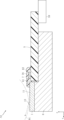
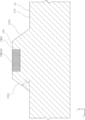
本実施形態のヘッド基板1は、単結晶半導体からなる。単結晶半導体としては、Siが好適である。当該ヘッド基板1の主面11の下流側寄りには、主走査方向xに延びる凸部13が一体に形成されている。この凸部13の断面形状は、主走査方向xについて一様である。
The
図5および図6に詳示するように、凸部13は、主面11と平行な頂面130と、この頂面130から副走査方向y両側につながって延び、主面11に至る一対の第1傾斜外面131を有する。一対の第1傾斜外面131は、頂面130から副走査方向yに離れるにしたがって低位となるように上記主面に対して傾斜する。一対の第1傾斜外面131の主面11に対する傾斜角度α1は、例えば50~60度である。本実施形態において、凸部13の寸法は、副走査方向y全幅H1が例えば200~300μm、高さH2が例えば150~180μm、頂面130の副走査方向y幅H3が例えば100~200μmである。なお、ヘッド基板1の主面11および凸部13の頂面は、(100)面である。
As shown in detail in FIGS. 5 and 6, the
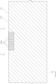
凸部13の頂面130には、当該頂面130の副走査方向y幅と同等の副走査方向所定幅であって、主走査方向xに延びる平面視領域に、所定深さの蓄熱部15が形成されている。この蓄熱部15は、凸部13の頂面130に上端が位置し、凸部13の深さ方向に所定長さで延びる多数の微小柱状蓄熱部材150を密集して埋設配置することにより形成されている。後記する製造方法によれば、微小柱状蓄熱部材150は、深掘りエッチング(DeepRIE)により柱状微小細孔150Aを形成し、約800~1100℃で熱酸化処理を行うことにより、柱状微小細孔150Aの内面をSiO2に変化させることにより形成される。熱酸化処理を行うことにより、SiO2に変化した部分が体積増加するため、少なくとも柱状微小細孔150Aの開口付近はSiO2で埋められる。この微小柱状蓄熱部材150は、できるだけ密集配置することが好ましいが、後記する製造方法において説明するように、それには、例えば内径1~10μm、深さ30~100μmの上記柱状微小細孔150Aを、主走査方向xおよび副走査方向yに1~3μmの間隔をあけて形成した上で、熱酸化処理を行うとよい。
On the
ヘッド基板1の主面11および上記のように蓄熱部15が設けられた凸部13には、少なくとも、これらを覆う絶縁層19、抵抗体層4、電極層3および保護層2がこの順で形成されている。
At least the
絶縁層19は、ヘッド基板1の主面11および凸部13を覆って形成されている。この絶縁層19は、後記する抵抗体層4および電極層3を形成するべき領域を覆うように形成される。絶縁層19は、絶縁性材料からなり、たとえばSiO2やSiNまたはTEOS(オルトケイ酸テトラエチル)からなり、本実施形態においては、TEOSが好適に採用されている。絶縁層19の厚さは特に限定されず、その一例を挙げるとたとえば5μm~15μmであり、好ましくは5μm~10μmである。
The insulating
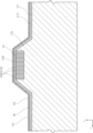
抵抗体層4は、絶縁層19を覆うように、主面11および凸部13にわたって形成されている。絶縁層19は、たとえばTaNからなる。抵抗体層4の厚さは特に限定されず、たとえば0.02μm~0.1μmであり、好ましくは0.08μm程度である。抵抗体層4は、後記する電極層3に覆われずに露出する部分が発熱部41を形成する。この発熱部41は、その多数が主走査方向xに配列され、その副走査方向yにおける形成領域は、凸部13の頂面130の副走査方向yの一部または全部を含んだ適宜領域とされる。抵抗体層4は、各発熱部41を主走査方向xについて独立させるため、少なくとも発熱部41を形成するべき副走査方向y領域については主走査方向xについて分離形成されている。
電極層3は、ヘッド基板1の上流側に形成される複数の個別電極層31と、ヘッド基板1の下流側に形成される共通電極層32とを含む。各個別電極層31は、概ね副走査方向yに延びる帯状をしており、それらの下流側先端は上記凸部13の副走査方向y適宜位置まで延びている。各個別電極層31の上流側端部には、個別パッド部311が形成されている。個別パッド部311は、接続基板5に搭載される駆動IC7とワイヤ61により接続される部分である。共通電極層32は、複数の櫛歯部324と、これら複数の櫛歯部324を共通につなげる共通部323とを有する。共通部323はヘッド基板1の上流側の縁に沿って主走査方向xに形成され、各櫛歯部324は、共通部323から分かれて副走査方向yに延びる帯状をしており、その上流側先端は、上記凸部13の副走査方向y適宜位置まで延び、各個別電極層31の先端に対して所定間隔を隔てて対向させられている。共通部323は、その主走査方向x両端から副走査方向yに折れ曲がってヘッド基板1の下流側に至る延長部325を有する。電極層3は、例えばCuからなり、その厚さは、例えば0.3~2.0μmである。上記したように、凸部13の頂面付近において、抵抗体層4のうち、個別電極層31と、これに先端部どうしが対向する共通電極層32の上記櫛歯部324とに覆われていない部分が各発熱部41を形成する。
The electrode layers 3 include a plurality of individual electrode layers 31 formed upstream of the
抵抗体層4および電極層3はさらに、保護層2で覆われている。保護層2は、絶縁性の材料からなり、例えばSiO2、SiN、SiC、AlN等からなる。保護層2の厚みは、例えば1.0~10μmである。
図5に示すように、保護層2は、パッド用開口21を有する。パッド用開口21は、複数の個別電極層31に設けた個別パッド部311を露出させている。
As shown in FIG. 5, the
接続基板5は、ヘッド基板1に対して副走査方向y上流側に隣接して配置されている。接続基板5は、例えばPCB基板であり、ドライバIC7やコネクタ59が搭載される。接続基板5は、主走査方向xを長手方向とする平面視長矩形状をしている。
The
ドライバIC7は、接続基板5上に搭載されており、複数の発熱部41に個別に通電させるために設けられる。ドライバIC7と上記各個別電極層31の各個別パッド部311間は、複数のワイヤ61によって接続される。ドライバIC7はまた、接続基板5上に形成された配線パターンに対して、ワイヤ62によって接続されている。ドライバIC7には、コネクタ59を介して外部から送信される印字信号が入力される。複数の発熱部41は、印字信号に従って個別に通電されることにより、選択的に発熱させられる。
The
ドライバIC7およびワイヤ61,62は、ヘッド基板1と接続基板5とに跨るようにして保護樹脂78で覆われている。保護樹脂78は、例えばエポキシ樹脂等の黒色の絶縁性樹脂が用いられる。
The
放熱部材8は、ヘッド基板1および接続基板5を支持しており、発熱部41により生じた熱の一部を外部へと放熱するために設けられる。放熱部材8は、例えばアルミ等の金属製である。
The
次に、サーマルプリントヘッドA1の製造方法の一例について、図7~図16を参照して説明する。 Next, an example of a method for manufacturing the thermal print head A1 will be described with reference to FIGS. 7 to 16. FIG.
まず、図7に示すように、材料基板1Aを用意する。材料基板1Aは、単結晶半導体からなり、たとえばSiウエハである。材料基板1Aは、平坦な主面11Aを有し、当該主面11Aは(100)面である。
First, as shown in FIG. 7, a
次いで、図8~図10に示すように、主面11Aに対し、例えば深掘りエッチングを施すことにより、内径1~10μm、深さ30~100μmの上記柱状微小細孔150Aを、主走査方向xおよび副走査方向yに1~3μmの間隔をあけて形成する。このように多数の柱状微小細孔150Aを形成する平面領域は、後記する凸部13の頂面130となる領域であり、例えば副走査方向y100~200μmで主走査方向xに延びる領域である。
Next, as shown in FIGS. 8 to 10, the
次いで、図10に示すように、上記多数の柱状微小細孔150Aに対して約800~1100℃で熱酸化処理を行うことにより、柱状微小細孔150Aの内面をSiO2に変化させて、多数の微小柱状蓄熱部材150からなる蓄熱部15を形成する。このとき、SiがSiO2に変化するとき、体積増加を伴うため、柱状微小細孔150Aの少なくとも開口付近はSiO2で埋められることになる。
Next, as shown in FIG. 10, the many
次いで、必要に応じて研磨するなどして、主面11Aに生じた酸化膜を除去した後、例えばKOHを用いた異方性エチングを行うことにより、図12に示すように、主走査方向xに略一様断面で延びる凸部13を形成する。このとき、上記のように多数の微小柱状蓄熱部材150が形成された領域をマスクとして機能させることができる。上記したように、凸部13は、頂面130およびこの頂面130を副走査方向yに挟んで位置する一対の傾斜外面(第1傾斜外面)131を有する。一対の傾斜外面131は、頂面130の副走査方向y両縁につながり、頂面130から副走査方向yに離れるにしたがい低位となるように傾斜する面である。
Next, after removing the oxide film formed on the
次いで、図13に示すように、絶縁層19を形成する。絶縁層の形成は、例えばCVDを用いてTEOSを堆積させることにより行う。
Next, as shown in FIG. 13, an insulating
次いで、図14に示すように、抵抗体膜4Aを形成する。抵抗体膜4Aの形成は、例えばスパッタリングにより絶縁層19上にTaNの薄膜を形成することによって行う。
Next, as shown in FIG. 14, a
次いで、図15に示すように、導電膜3Aを形成する。導電膜3Aの形成は、例えばめっきやスパッタリングによりCuからなる層を形成することによって行う。
Next, as shown in FIG. 15, a
次いで、図16に示すように、導電膜3Aおよび抵抗体膜4Aに選択的なエッチングを施すことにより、主走査方向xに分離された抵抗体層4、この抵抗体層4を発熱部41を残して覆う個別電極層31、および共通電極層32の櫛歯部324を形成する。
Next, as shown in FIG. 16, by selectively etching the
次いで、保護層2を形成する、保護層2の形成は、例えばCVDを用いて絶縁層19、電極層3および抵抗体層4上にSiNおよびSiCを堆積させることにより行われる。また、保護層2をエッチング等により部分的に除去することにより、パッド用開口21を形成する。この後は、放熱部材8上へのヘッド基板1および接続基板5の組付け、接続基板5へのドライバIC7接続の搭載、ワイヤ61,62のボンディング、保護樹脂78の形成等を行うことにより、図1~図6に示したサーマルプリントヘッドA1が得られる。
The formation of the
次に、第1実施形態に係るサーマルプリントヘッドA1の作用について説明する。 Next, operation of the thermal print head A1 according to the first embodiment will be described.
複数の発熱部41は、ヘッド基板1に設けた凸部13の頂面付近に配列されるため、印字媒体はプラテンローラ91を介して確実に発熱部41に押圧される。凸部13は、単結晶半導体に対して異方性エッチングを施すことにより形成されるため、その断面は主走査方向xについて一様となる。印字媒体の発熱部41に対する押圧接触状態は、主走査方向x各所において一定となる。これらのことは、ヘッド基板1の製造ロットが異なっても変わらない。そしてこのことは、印字品質の向上につながる。
Since the plurality of
ヘッド基板1の材料であるSiウエハは、SiO2などの絶縁材料と比較して熱伝導性がよく、何らの手当も行わないと発熱部41が発する熱を無駄に放熱部材8に向けて漏出させ、高速印字に不向きとなるが、このサーマルプリントヘッドA1の凸部13には、発熱部41の直下にSiO2からなる蓄熱部15が所定深さで設けられているため、発熱部41が発する熱の無駄な漏出が防がれ、高速印字にも適するようになる。
A Si wafer, which is the material of the
図17および図18は、本発明の第2実施形態に係るサーマルプリントヘッドを示す。このサーマルプリントヘッドA2は、第1実施形態に係るサーマルプリントヘッドA1と比較して、凸部13の形態が異なり、その余の構成は同じである。図17および図18においては、第1実施形態に係るサーマルプリントヘッドA1と同一の部分または部材には同一の符号を付し、以下においては適宜説明を省略する。
17 and 18 show a thermal printhead according to a second embodiment of the invention. The thermal print head A2 differs from the thermal print head A1 according to the first embodiment in the shape of the
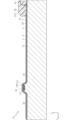
本実施形態では、ヘッド基板1に設ける凸部13は、頂面130と、この頂面130の副走査方向y両縁につながる一対の第2傾斜外面132と、当該一対の第2傾斜外面132の副走査方向y外縁につながり、主面11に至る一対の第1傾斜外面131とを有する。一対の第1傾斜外面131は、副走査方向yに頂面から離れるにしたがい低位となるように傾斜する面であり、主面11に対する傾斜角度α1は、例えば50~60度である。一対の第2傾斜外面132もまた、副走査方向yに頂面130から離れるにしたがい低位となるように傾斜する面であり、主面11に対する傾斜角度α2は、例えば25~35度である。本実施形態においても、凸部13は、主走査方向xについて断面略一様に形成されている。
In this embodiment, the
本実施形態においても、凸部13の頂面130には、当該頂面130の副走査方向y幅と同等の副走査方向所定幅であって、主走査方向xに延びる平面視領域に、第1実施形態について説明したのと同様にして、所定深さの蓄熱部15が形成されている。すなわち、この蓄熱部15は、凸部13の頂面130に上端が位置し、凸部13の深さ方向に所定長さで延びる多数の微小柱状蓄熱部材150を密集して埋設配置することにより形成されている。微小柱状蓄熱部材150は、深掘りエッチングにより柱状微小細孔150Aを形成し、約800~1100℃で熱酸化処理を行うことにより、柱状微小細孔150Aの内面をSiO2に変化させることにより形成される。
In the present embodiment as well, the
ヘッド基板1の主面11および上記のように蓄熱部15が設けられた凸部13には、第1実施形態と同様に、絶縁層19、抵抗体層4、電極層3および保護層2がこの順で形成されている。
An insulating
ヘッド基板1に隣接して配置される接続基板5およびこれらヘッド基板1および接続基板5を搭載する放熱部材8の構成は、第1実施形態と同様である。
The configuration of the
次に、上記した第2実施形態に係るサーマルプリントヘッドA2の製造方法の一例について、図19~図28を参照して説明する。 Next, an example of a method for manufacturing the thermal print head A2 according to the second embodiment will be described with reference to FIGS. 19 to 28. FIG.
まず、図19に示すように、材料基板1Aを用意する。材料基板1Aは、単結晶半導体からなり、例えばSiウエハである。材料基板1Aは、平坦な主面11Aを有し、当該主面11Aは(100)面である。
First, as shown in FIG. 19, a
次いで、図20および図21に示すように、主面11Aに対し、例えば深掘りエッチングを施すことにより、内径1~10μm、深さ30~100μmの上記柱状微小細孔150Aを、主走査方向xおよび副走査方向yに1~3μmの間隔をあけて形成する。このように多数の柱状微小細孔150Aを形成する平面領域は、後記する凸部13の頂面130となる領域であり、例えば副走査方向y100~200μmで、主走査方向xに延びる領域である。
Next, as shown in FIGS. 20 and 21, the
次いで、図22に示すように、上記多数の柱状微小細孔150Aに対して約800~1100℃で熱酸化処理を行うことにより、柱状微小細孔150Aの内面をSiO2に変化させて、多数の微小柱状蓄熱部材150からなる蓄熱部15を形成する。このとき、SiがSiO2に変化する際に体積増加を伴うため、柱状微小細孔150Aの少なくとも開口付近はSiO2で埋められることになる。
Next, as shown in FIG. 22, the many
次いで、必要に応じて主面11Aを研磨するなどして、主面11Aに生じた酸化膜を除去した後、主面11Aを所定のマスク層で覆った状態で、例えばKOHを用いた異方性エッチングを行うことにより、図23に示すように、主走査方向xに一様断面で延びる凸部中間体13Aを形成する。凸部中間体13Aは、頂面130Aおよびこの頂面130Aを副走査方向yに挟んで位置する一対の傾斜外面131Aを有する。この一対の傾斜外面131Aは、その主面11に近い一部が一対の第1傾斜外面131となるべき面である。頂面130Aは、材料基板1Aの主面11Aが残った平坦面であり、(100)面である。一対の傾斜外面131Aは、頂面130Aの副走査方向yにつながり、頂面130Aから副走査方向yに離れるにしたがい低位となるように傾斜する平面である。この状態において、凸部中間体13Aの頂面130Aには、上記のように形成した多数の微小柱状蓄熱部材150の上端が表れている。一対の傾斜外面131Aの主面11とのなす角度は、50~60度である。
Next, after removing the oxide film formed on the
次いで、例えばTMAHを用いた追加の異方性エッチングを行うことにより、図24に示すように、凸部中間体13Aに一対の第2傾斜外面132を形成することにより、一対の第1傾斜外面131と一対の第2傾斜外面132を有する凸部13を完成させる。この追加の異方性エッチングは、凸部中間体13Aの頂面130Aに上端が表れる多数の微小柱状蓄熱部材150をマスクとして利用しつつ行うことができる。一対の第2傾斜外面132の主面11とのなす角度α2は、25~35度である。
Then, as shown in FIG. 24, by performing additional anisotropic etching using, for example, TMAH, a pair of second inclined
次いで、図25に示すように、絶縁層19を形成する。絶縁層19の形成は、例えばCVDを用いてTEOSを堆積させることにより行う。
Next, as shown in FIG. 25, an insulating
次いで、図26に示すように、抵抗体膜4Aを形成する。抵抗体膜4Aは、例えばスパッタリングにより絶縁層19上にTaNの薄膜を形成することによって行う。
Next, as shown in FIG. 26, a
次いで、図27に示すように、導電膜3Aを形成する。導電膜3Aの形成は、例えばめっきやスパッタリングによりCuからなる層を形成することによって行う。
Next, as shown in FIG. 27, a
次いで、図28に示すように、導電膜3Aおよび抵抗体膜4Aに選択的なエッチングを施すことにより、主走査方向xに分離された抵抗体層4、この抵抗体層4を発熱部41を残して覆う個別電極層31、および共通電極層32の櫛歯部324を形成する。
Next, as shown in FIG. 28, by selectively etching the
次いで、保護層2を形成する。保護層2の形成は、例えばCVDを用いて絶縁層19、電極層3および抵抗体層4上にSiNおよびSiCを堆積させることにより行われる。また、保護層2をエッチング等により部分的に除去することにより、パッド用開口21を形成する。この後は、放熱部材8上へのヘッド基板1および接続基板5の組付け、接続基板5へのドライバIC7の搭載、ワイヤ61,62のボンディング、保護樹脂78の形成等を行うことにより、図17および図18に示したサーマルプリントヘッドA2が得られる。
Next,
この第2実施形態に係るサーマルプリントヘッドA2もまた、第1実施形態に係るサーマルプリントヘッドA1について上述したのと同様の作用を有する。 The thermal print head A2 according to the second embodiment also has the same function as the thermal print head A1 according to the first embodiment.
加えて本実施形態に係るサーマルプリントヘッドA2においては、凸部13の傾斜外面が第1傾斜外面131と第2傾斜外面132との2段階の傾斜外面で構成されているため、プラテンローラ91を介して凸部13に押圧される印字媒体を引っ掛かりなくより円滑に副走査方向yに送ることができる。
In addition, in the thermal print head A2 according to the present embodiment, the inclined outer surface of the
もちろん、本発明の範囲は上述した実施形態に限定されるものではなく、各請求項に記載した事項の範囲内でのあらゆる変更は、すべて本発明の範囲に含まれる。 Of course, the scope of the present invention is not limited to the embodiments described above, and all modifications within the scope of matters described in each claim are included in the scope of the present invention.
例えば、第2実施形態に係るサーマルプリントヘッドA2の構成において、凸部13の傾斜外面として、第1傾斜外面131、第2傾斜外面132に加え、第2傾斜外面132と頂面130との間に、主面11となす角度が第2傾斜外面132よりも小さい第3傾斜外面(図示せず)を設け、凸部13の表面をよりなだらかなものとすることも、本発明の範囲に含まれる。
For example, in the configuration of the thermal print head A<b>2 according to the second embodiment, the inclined outer surfaces of the
さらに、複数の発熱部41に関して、主走査方向xに独立配置した抵抗体層の露出部に選択的に通電して発熱させるあらゆる発熱部の形態を採用できることは、もちろんである。
Further, with respect to the plurality of
A1、A2:サーマルプリントヘッド
1 :ヘッド基板
1A :材料基板
2 :保護層
3 :電極層
3A :導電膜
4 :抵抗体層
4A :抵抗体膜
5 :接続基板
7 :ドライバIC
8 :放熱部材
11 :主面
11A :主面
13 :凸部
13A :凸部中間体
15 :蓄熱部
19 :絶縁層
21 :パッド用開口
31 :個別電極層
32 :共通電極層
41 :発熱部
59 :コネクタ
61 :ワイヤ
62 :ワイヤ
78 :保護樹脂
91 :プラテンローラ
130 :頂面
130A :頂面
131 :第1傾斜外面
131A :傾斜外面
132 :第2傾斜外面
150 :微小柱状蓄熱部材
150A :柱状微小細孔
311 ;電極パッド部
323 :共通部
324 :櫛歯部
325 :延長部
x :主走査方向
y :副走査方向
α1、α2:角度
A1, A2: Thermal print head 1:
8: heat dissipation member 11:
Claims (2)
主面を有する単結晶半導体からなる材料基板の上記主面における上記凸部の上記頂面となるべき領域に上記多数の微小柱状蓄熱部材を埋設配置した後、
上記材料基板の上記主面に対して異方性エッチングを行うことにより、上記一対の傾斜外面と上記頂面とを有する上記凸部を形成するに際し、
上記多数の微小柱状蓄熱部材は、Siウエハからなる上記材料基板の上記主面に深掘りエッチングにより上記材料基板の厚み方向に延びる多数の微小細孔を形成し、熱酸化処理を行うことにより上記多数の微小細孔をSiO2に変化させることにより形成し、
上記一対の第1傾斜外面は、上記材料基板の(100)面である上記主面に対し、上記材料基板の上記主面のうち、上記多数の微小蓄熱部材が埋設形成された領域をマスクとして異方性エッチングを行うことにより形成することを特徴とする、サーマルプリントヘッドの製造方法。 A substrate having a main surface, a convex portion formed on the main surface of the substrate and extending in the main scanning direction, and a plurality of heat generating portions arranged in the main scanning direction on the top surface of the convex portion, An upper end of the convex portion is positioned on the top surface thereof, and a large number of micro-columnar heat storage members extending for a predetermined length in the depth direction of the convex portion extend for a predetermined length in the main scanning direction with a predetermined width in the sub-scanning direction. A heat storage portion is formed by embedding in a predetermined region, and the convex portion is connected to the top surface on both sides of the top surface in the sub-scanning direction and separated from the top surface in the sub-scanning direction. a pair of first slanted outer surfaces slanted with respect to the main surface so as to be lowered according to
After burying and arranging the numerous micro-columnar heat storage members in regions to be the top surfaces of the protrusions on the main surface of a material substrate having a main surface and made of a single crystal semiconductor,
When forming the convex portion having the pair of inclined outer surfaces and the top surface by anisotropically etching the main surface of the material substrate,
The large number of micro-columnar heat storage members are formed by forming a large number of micropores extending in the thickness direction of the material substrate by deep etching in the main surface of the material substrate made of a Si wafer, and performing thermal oxidation treatment. Forming by converting a large number of micropores into SiO2,
The pair of first inclined outer surfaces are formed by using, as a mask, a region of the main surface of the material substrate in which the numerous micro heat storage members are embedded, with respect to the main surface which is the (100) plane of the material substrate. A method of manufacturing a thermal print head, characterized by forming the thermal print head by anisotropic etching .
主面を有する単結晶半導体からなる材料基板の上記主面における上記凸部の上記頂面となるべき領域に上記多数の微小柱状蓄熱部材を埋設配置した後、
上記材料基板の上記主面に対して異方性エッチングを行うことにより、上記一対の第1傾斜外面と、上記第2傾斜外面と、上記頂面とを有する上記凸部を形成するに際し、
上記多数の微小柱状蓄熱部材は、Siウエハからなる上記材料基板の上記主面に深掘りエッチングにより上記材料基板の厚み方向に延びる多数の微小細孔を形成し、熱酸化処理を行うことにより上記多数の微小細孔をSiO2に変化させることにより形成し、
上記一対の第1傾斜外面および上記一対の第2傾斜外面は、上記材料基板の(100)面である上記主面に対して異方性エッチングを行うことにより上記一対の第1傾斜外面となるべき一対の傾斜外面を形成した後、上記材料基板の上記主面のうち、上記多数の微小蓄熱部材が埋設形成された領域をマスクとして追加の異方性エッチングを行うことにより、上記一対の第2傾斜外面を形成することを特徴とする、サーマルプリントヘッドの製造方法。 A substrate having a main surface, a convex portion formed on the main surface of the substrate and extending in the main scanning direction, and a plurality of heat generating portions arranged in the main scanning direction on the top surface of the convex portion, An upper end of the convex portion is positioned on the top surface thereof, and a large number of micro-columnar heat storage members extending for a predetermined length in the depth direction of the convex portion extend for a predetermined length in the main scanning direction with a predetermined width in the sub-scanning direction. A heat storage portion is formed by embedding in a predetermined region, and the convex portion is connected to the top surface on both sides of the top surface in the sub-scanning direction and separated from the top surface in the sub-scanning direction. a pair of second inclined outer surfaces inclined with respect to the main surface so as to be lower in accordance with the above-mentioned top surface; a pair of first inclined outer surfaces inclined with respect to the main surface at a larger angle than the pair of second inclined outer surfaces so that the surface becomes lower as the distance from the surface increases in the sub-scanning direction. A manufacturing method of
After burying and arranging the numerous micro-columnar heat storage members in regions to be the top surfaces of the protrusions on the main surface of a material substrate having a main surface and made of a single crystal semiconductor,
When forming the convex portion having the pair of first inclined outer surfaces, the second inclined outer surface, and the top surface by performing anisotropic etching on the main surface of the material substrate,
The large number of micro-columnar heat storage members are formed by forming a large number of micropores extending in the thickness direction of the material substrate by deep etching in the main surface of the material substrate made of a Si wafer, and performing thermal oxidation treatment. Forming by converting a large number of micropores into SiO2,
The pair of first inclined outer surfaces and the pair of second inclined outer surfaces become the pair of first inclined outer surfaces by performing anisotropic etching on the main surface, which is the (100) plane of the material substrate. After forming the pair of inclined outer surfaces, additional anisotropic etching is performed using, as a mask, the region in which the numerous small heat storage members are embedded in the main surface of the material substrate, thereby forming the pair of second inclined surfaces. A method of manufacturing a thermal printhead, comprising forming a two-slanted outer surface .
Priority Applications (2)
| Application Number | Priority Date | Filing Date | Title |
|---|---|---|---|
| JP2019117056A JP7269802B2 (en) | 2019-06-25 | 2019-06-25 | Thermal print head and manufacturing method thereof |
| US16/908,143 US11279145B2 (en) | 2019-06-25 | 2020-06-22 | Thermal print head and method of manufacturing the same |
Applications Claiming Priority (1)
| Application Number | Priority Date | Filing Date | Title |
|---|---|---|---|
| JP2019117056A JP7269802B2 (en) | 2019-06-25 | 2019-06-25 | Thermal print head and manufacturing method thereof |
Publications (2)
| Publication Number | Publication Date |
|---|---|
| JP2021003809A JP2021003809A (en) | 2021-01-14 |
| JP7269802B2 true JP7269802B2 (en) | 2023-05-09 |
Family
ID=74044377
Family Applications (1)
| Application Number | Title | Priority Date | Filing Date |
|---|---|---|---|
| JP2019117056A Active JP7269802B2 (en) | 2019-06-25 | 2019-06-25 | Thermal print head and manufacturing method thereof |
Country Status (2)
| Country | Link |
|---|---|
| US (1) | US11279145B2 (en) |
| JP (1) | JP7269802B2 (en) |
Families Citing this family (1)
| Publication number | Priority date | Publication date | Assignee | Title |
|---|---|---|---|---|
| JP2023010023A (en) * | 2021-07-08 | 2023-01-20 | ローム株式会社 | Thermal print head, and manufacturing method of thermal print head |
Citations (6)
| Publication number | Priority date | Publication date | Assignee | Title |
|---|---|---|---|---|
| JP2003165241A (en) | 2001-12-03 | 2003-06-10 | Alps Electric Co Ltd | Thermal head |
| JP2004303744A (en) | 2003-03-28 | 2004-10-28 | Denso Corp | Monolithic microwave integrated circuit and its fabrication method |
| JP2004342774A (en) | 2003-05-14 | 2004-12-02 | Fuji Electric Device Technology Co Ltd | Method for manufacturing semiconductor device |
| US20070042606A1 (en) | 2005-08-19 | 2007-02-22 | Honeywell International Inc. | Creating novel structures using deep trenching of oriented silicon substrates |
| JP2014231216A (en) | 2012-08-29 | 2014-12-11 | ローム株式会社 | Thermal print head and thermal printer |
| JP2019014233A (en) | 2017-06-08 | 2019-01-31 | ローム株式会社 | Thermal print head |
Family Cites Families (5)
| Publication number | Priority date | Publication date | Assignee | Title |
|---|---|---|---|---|
| JPS6295239A (en) | 1985-10-23 | 1987-05-01 | Alps Electric Co Ltd | Thermal head |
| EP1226951A3 (en) | 2001-01-29 | 2003-03-12 | Alps Electric Co., Ltd. | Power-saving thermal head |
| US6767081B2 (en) * | 2001-12-03 | 2004-07-27 | Alps Electric Co., Ltd. | Thermal head |
| JP2007269036A (en) | 2007-06-04 | 2007-10-18 | Rohm Co Ltd | Method for adjusting resistance value of heating element of thin-film thermal print head |
| JP6650264B2 (en) * | 2015-12-25 | 2020-02-19 | ローム株式会社 | Thermal print head |
-
2019
- 2019-06-25 JP JP2019117056A patent/JP7269802B2/en active Active
-
2020
- 2020-06-22 US US16/908,143 patent/US11279145B2/en active Active
Patent Citations (6)
| Publication number | Priority date | Publication date | Assignee | Title |
|---|---|---|---|---|
| JP2003165241A (en) | 2001-12-03 | 2003-06-10 | Alps Electric Co Ltd | Thermal head |
| JP2004303744A (en) | 2003-03-28 | 2004-10-28 | Denso Corp | Monolithic microwave integrated circuit and its fabrication method |
| JP2004342774A (en) | 2003-05-14 | 2004-12-02 | Fuji Electric Device Technology Co Ltd | Method for manufacturing semiconductor device |
| US20070042606A1 (en) | 2005-08-19 | 2007-02-22 | Honeywell International Inc. | Creating novel structures using deep trenching of oriented silicon substrates |
| JP2014231216A (en) | 2012-08-29 | 2014-12-11 | ローム株式会社 | Thermal print head and thermal printer |
| JP2019014233A (en) | 2017-06-08 | 2019-01-31 | ローム株式会社 | Thermal print head |
Also Published As
| Publication number | Publication date |
|---|---|
| US11279145B2 (en) | 2022-03-22 |
| JP2021003809A (en) | 2021-01-14 |
| US20200406631A1 (en) | 2020-12-31 |
Similar Documents
| Publication | Publication Date | Title |
|---|---|---|
| JP6371529B2 (en) | Thermal print head, thermal printer | |
| CN108944063B (en) | Thermal print head and method of manufacturing thermal print head | |
| JP7269802B2 (en) | Thermal print head and manufacturing method thereof | |
| JP7413066B2 (en) | Thermal print head manufacturing method, thermal print head and thermal printer | |
| JP7284640B2 (en) | thermal print head | |
| JP7093226B2 (en) | Thermal print head | |
| JP6209019B2 (en) | Thermal print head, thermal printer | |
| JP6786669B2 (en) | Thermal printhead, thermal printer | |
| JP6557066B2 (en) | Thermal print head manufacturing method and thermal print head | |
| JP5802032B2 (en) | Thermal print head | |
| JP7297564B2 (en) | Thermal print head and manufacturing method thereof | |
| JP2021115854A (en) | Thermal print head and method of manufacturing thermal print head | |
| JP5670076B2 (en) | Thermal print head and manufacturing method thereof | |
| JP6341723B2 (en) | Thermal print head and thermal printer | |
| JP7151054B2 (en) | Thermal print head and manufacturing method thereof | |
| JP6422225B2 (en) | Thermal head | |
| WO2021149617A1 (en) | Thermal print head and method for manufacturing thermal print head | |
| JP2023082289A (en) | Thermal print head, and manufacturing method of thermal print head | |
| JP2019098667A (en) | Thermal print head | |
| JP7360880B2 (en) | Thermal print head and its manufacturing method | |
| JP7398244B2 (en) | Method for forming heat storage layer and method for manufacturing thermal print head | |
| JP7219634B2 (en) | thermal print head | |
| US20200391517A1 (en) | Thermal print head and method of manufacturing thermal print head | |
| JP2023121941A (en) | thermal print head | |
| JP2024009481A (en) | Thermal print head and manufacturing method for thermal print head |
Legal Events
| Date | Code | Title | Description |
|---|---|---|---|
| A621 | Written request for application examination |
Free format text: JAPANESE INTERMEDIATE CODE: A621 Effective date: 20220516 |
|
| A977 | Report on retrieval |
Free format text: JAPANESE INTERMEDIATE CODE: A971007 Effective date: 20230112 |
|
| A131 | Notification of reasons for refusal |
Free format text: JAPANESE INTERMEDIATE CODE: A131 Effective date: 20230117 |
|
| A521 | Request for written amendment filed |
Free format text: JAPANESE INTERMEDIATE CODE: A523 Effective date: 20230320 |
|
| TRDD | Decision of grant or rejection written | ||
| A01 | Written decision to grant a patent or to grant a registration (utility model) |
Free format text: JAPANESE INTERMEDIATE CODE: A01 Effective date: 20230404 |
|
| A61 | First payment of annual fees (during grant procedure) |
Free format text: JAPANESE INTERMEDIATE CODE: A61 Effective date: 20230424 |
|
| R150 | Certificate of patent or registration of utility model |
Ref document number: 7269802 Country of ref document: JP Free format text: JAPANESE INTERMEDIATE CODE: R150 |