JP6335538B2 - プラズマ処理室用のガス分配部材を製造する方法 - Google Patents
プラズマ処理室用のガス分配部材を製造する方法 Download PDFInfo
- Publication number
- JP6335538B2 JP6335538B2 JP2014025393A JP2014025393A JP6335538B2 JP 6335538 B2 JP6335538 B2 JP 6335538B2 JP 2014025393 A JP2014025393 A JP 2014025393A JP 2014025393 A JP2014025393 A JP 2014025393A JP 6335538 B2 JP6335538 B2 JP 6335538B2
- Authority
- JP
- Japan
- Prior art keywords
- carbon
- gas distribution
- shaped
- distribution member
- gas
- Prior art date
- Legal status (The legal status is an assumption and is not a legal conclusion. Google has not performed a legal analysis and makes no representation as to the accuracy of the status listed.)
- Active
Links
- 238000009826 distribution Methods 0.000 title claims description 125
- 238000004519 manufacturing process Methods 0.000 title claims description 7
- 239000007789 gas Substances 0.000 claims description 219
- OKTJSMMVPCPJKN-UHFFFAOYSA-N Carbon Chemical compound [C] OKTJSMMVPCPJKN-UHFFFAOYSA-N 0.000 claims description 117
- 229910052799 carbon Inorganic materials 0.000 claims description 113
- 238000000034 method Methods 0.000 claims description 69
- 239000000463 material Substances 0.000 claims description 38
- 238000000151 deposition Methods 0.000 claims description 19
- 230000008569 process Effects 0.000 claims description 18
- 238000003754 machining Methods 0.000 claims description 17
- 239000004065 semiconductor Substances 0.000 claims description 16
- QVGXLLKOCUKJST-UHFFFAOYSA-N atomic oxygen Chemical compound [O] QVGXLLKOCUKJST-UHFFFAOYSA-N 0.000 claims description 11
- 229910052760 oxygen Inorganic materials 0.000 claims description 11
- 239000001301 oxygen Substances 0.000 claims description 11
- 230000008021 deposition Effects 0.000 claims description 8
- 238000005553 drilling Methods 0.000 claims description 6
- 229910002804 graphite Inorganic materials 0.000 claims description 5
- 239000010439 graphite Substances 0.000 claims description 5
- 238000010438 heat treatment Methods 0.000 claims description 5
- 238000001020 plasma etching Methods 0.000 claims description 5
- 238000000623 plasma-assisted chemical vapour deposition Methods 0.000 claims description 5
- 238000004380 ashing Methods 0.000 claims description 4
- 125000004432 carbon atom Chemical group C* 0.000 claims description 4
- 239000007921 spray Substances 0.000 claims description 4
- 238000005229 chemical vapour deposition Methods 0.000 claims description 3
- 229910052739 hydrogen Inorganic materials 0.000 claims description 3
- 239000001257 hydrogen Substances 0.000 claims description 3
- 230000035699 permeability Effects 0.000 claims description 3
- UFHFLCQGNIYNRP-UHFFFAOYSA-N Hydrogen Chemical compound [H][H] UFHFLCQGNIYNRP-UHFFFAOYSA-N 0.000 claims description 2
- 238000002834 transmittance Methods 0.000 claims description 2
- 238000005516 engineering process Methods 0.000 claims 1
- HBMJWWWQQXIZIP-UHFFFAOYSA-N silicon carbide Chemical compound [Si+]#[C-] HBMJWWWQQXIZIP-UHFFFAOYSA-N 0.000 description 45
- 229910010271 silicon carbide Inorganic materials 0.000 description 44
- 239000000758 substrate Substances 0.000 description 21
- UGFAIRIUMAVXCW-UHFFFAOYSA-N Carbon monoxide Chemical compound [O+]#[C-] UGFAIRIUMAVXCW-UHFFFAOYSA-N 0.000 description 5
- 229910002091 carbon monoxide Inorganic materials 0.000 description 5
- 238000004891 communication Methods 0.000 description 5
- 238000005530 etching Methods 0.000 description 5
- 229910052736 halogen Inorganic materials 0.000 description 4
- 150000002367 halogens Chemical class 0.000 description 4
- VYPSYNLAJGMNEJ-UHFFFAOYSA-N Silicium dioxide Chemical compound O=[Si]=O VYPSYNLAJGMNEJ-UHFFFAOYSA-N 0.000 description 3
- XUIMIQQOPSSXEZ-UHFFFAOYSA-N Silicon Chemical compound [Si] XUIMIQQOPSSXEZ-UHFFFAOYSA-N 0.000 description 3
- 238000005260 corrosion Methods 0.000 description 3
- 230000007797 corrosion Effects 0.000 description 3
- 229910052710 silicon Inorganic materials 0.000 description 3
- 239000010703 silicon Substances 0.000 description 3
- CURLTUGMZLYLDI-UHFFFAOYSA-N Carbon dioxide Chemical compound O=C=O CURLTUGMZLYLDI-UHFFFAOYSA-N 0.000 description 2
- 229910052782 aluminium Inorganic materials 0.000 description 2
- XAGFODPZIPBFFR-UHFFFAOYSA-N aluminium Chemical compound [Al] XAGFODPZIPBFFR-UHFFFAOYSA-N 0.000 description 2
- 230000008901 benefit Effects 0.000 description 2
- 230000015572 biosynthetic process Effects 0.000 description 2
- 238000005219 brazing Methods 0.000 description 2
- 239000003989 dielectric material Substances 0.000 description 2
- 239000012530 fluid Substances 0.000 description 2
- 238000000227 grinding Methods 0.000 description 2
- VNWKTOKETHGBQD-UHFFFAOYSA-N methane Chemical compound C VNWKTOKETHGBQD-UHFFFAOYSA-N 0.000 description 2
- 239000000203 mixture Substances 0.000 description 2
- 239000002245 particle Substances 0.000 description 2
- 229920002120 photoresistant polymer Polymers 0.000 description 2
- 239000007787 solid Substances 0.000 description 2
- 239000000126 substance Substances 0.000 description 2
- XLYOFNOQVPJJNP-UHFFFAOYSA-N water Substances O XLYOFNOQVPJJNP-UHFFFAOYSA-N 0.000 description 2
- 230000002411 adverse Effects 0.000 description 1
- 238000007743 anodising Methods 0.000 description 1
- 150000001721 carbon Chemical group 0.000 description 1
- 229910002092 carbon dioxide Inorganic materials 0.000 description 1
- 239000001569 carbon dioxide Substances 0.000 description 1
- 230000008859 change Effects 0.000 description 1
- 238000002485 combustion reaction Methods 0.000 description 1
- 239000004020 conductor Substances 0.000 description 1
- 238000011109 contamination Methods 0.000 description 1
- 230000006378 damage Effects 0.000 description 1
- 229920001971 elastomer Polymers 0.000 description 1
- 239000000806 elastomer Substances 0.000 description 1
- 238000010894 electron beam technology Methods 0.000 description 1
- 230000003628 erosive effect Effects 0.000 description 1
- NBVXSUQYWXRMNV-UHFFFAOYSA-N fluoromethane Chemical compound FC NBVXSUQYWXRMNV-UHFFFAOYSA-N 0.000 description 1
- 150000002431 hydrogen Chemical class 0.000 description 1
- 238000010884 ion-beam technique Methods 0.000 description 1
- 239000007788 liquid Substances 0.000 description 1
- 230000007246 mechanism Effects 0.000 description 1
- 229910052751 metal Inorganic materials 0.000 description 1
- 239000002184 metal Substances 0.000 description 1
- 238000012986 modification Methods 0.000 description 1
- 230000004048 modification Effects 0.000 description 1
- 230000003647 oxidation Effects 0.000 description 1
- 238000007254 oxidation reaction Methods 0.000 description 1
- 230000000704 physical effect Effects 0.000 description 1
- 238000005498 polishing Methods 0.000 description 1
- 229920000642 polymer Polymers 0.000 description 1
- 235000012239 silicon dioxide Nutrition 0.000 description 1
- 239000000377 silicon dioxide Substances 0.000 description 1
- 229910052814 silicon oxide Inorganic materials 0.000 description 1
- 238000004544 sputter deposition Methods 0.000 description 1
Images
Classifications
-
- C—CHEMISTRY; METALLURGY
- C23—COATING METALLIC MATERIAL; COATING MATERIAL WITH METALLIC MATERIAL; CHEMICAL SURFACE TREATMENT; DIFFUSION TREATMENT OF METALLIC MATERIAL; COATING BY VACUUM EVAPORATION, BY SPUTTERING, BY ION IMPLANTATION OR BY CHEMICAL VAPOUR DEPOSITION, IN GENERAL; INHIBITING CORROSION OF METALLIC MATERIAL OR INCRUSTATION IN GENERAL
- C23C—COATING METALLIC MATERIAL; COATING MATERIAL WITH METALLIC MATERIAL; SURFACE TREATMENT OF METALLIC MATERIAL BY DIFFUSION INTO THE SURFACE, BY CHEMICAL CONVERSION OR SUBSTITUTION; COATING BY VACUUM EVAPORATION, BY SPUTTERING, BY ION IMPLANTATION OR BY CHEMICAL VAPOUR DEPOSITION, IN GENERAL
- C23C16/00—Chemical coating by decomposition of gaseous compounds, without leaving reaction products of surface material in the coating, i.e. chemical vapour deposition [CVD] processes
- C23C16/44—Chemical coating by decomposition of gaseous compounds, without leaving reaction products of surface material in the coating, i.e. chemical vapour deposition [CVD] processes characterised by the method of coating
- C23C16/455—Chemical coating by decomposition of gaseous compounds, without leaving reaction products of surface material in the coating, i.e. chemical vapour deposition [CVD] processes characterised by the method of coating characterised by the method used for introducing gases into reaction chamber or for modifying gas flows in reaction chamber
- C23C16/45563—Gas nozzles
- C23C16/45565—Shower nozzles
-
- H—ELECTRICITY
- H01—ELECTRIC ELEMENTS
- H01J—ELECTRIC DISCHARGE TUBES OR DISCHARGE LAMPS
- H01J37/00—Discharge tubes with provision for introducing objects or material to be exposed to the discharge, e.g. for the purpose of examination or processing thereof
- H01J37/32—Gas-filled discharge tubes
- H01J37/32431—Constructional details of the reactor
- H01J37/32532—Electrodes
- H01J37/32541—Shape
-
- B—PERFORMING OPERATIONS; TRANSPORTING
- B05—SPRAYING OR ATOMISING IN GENERAL; APPLYING FLUENT MATERIALS TO SURFACES, IN GENERAL
- B05D—PROCESSES FOR APPLYING FLUENT MATERIALS TO SURFACES, IN GENERAL
- B05D5/00—Processes for applying liquids or other fluent materials to surfaces to obtain special surface effects, finishes or structures
-
- C—CHEMISTRY; METALLURGY
- C23—COATING METALLIC MATERIAL; COATING MATERIAL WITH METALLIC MATERIAL; CHEMICAL SURFACE TREATMENT; DIFFUSION TREATMENT OF METALLIC MATERIAL; COATING BY VACUUM EVAPORATION, BY SPUTTERING, BY ION IMPLANTATION OR BY CHEMICAL VAPOUR DEPOSITION, IN GENERAL; INHIBITING CORROSION OF METALLIC MATERIAL OR INCRUSTATION IN GENERAL
- C23C—COATING METALLIC MATERIAL; COATING MATERIAL WITH METALLIC MATERIAL; SURFACE TREATMENT OF METALLIC MATERIAL BY DIFFUSION INTO THE SURFACE, BY CHEMICAL CONVERSION OR SUBSTITUTION; COATING BY VACUUM EVAPORATION, BY SPUTTERING, BY ION IMPLANTATION OR BY CHEMICAL VAPOUR DEPOSITION, IN GENERAL
- C23C16/00—Chemical coating by decomposition of gaseous compounds, without leaving reaction products of surface material in the coating, i.e. chemical vapour deposition [CVD] processes
- C23C16/01—Chemical coating by decomposition of gaseous compounds, without leaving reaction products of surface material in the coating, i.e. chemical vapour deposition [CVD] processes on temporary substrates, e.g. substrates subsequently removed by etching
-
- C—CHEMISTRY; METALLURGY
- C23—COATING METALLIC MATERIAL; COATING MATERIAL WITH METALLIC MATERIAL; CHEMICAL SURFACE TREATMENT; DIFFUSION TREATMENT OF METALLIC MATERIAL; COATING BY VACUUM EVAPORATION, BY SPUTTERING, BY ION IMPLANTATION OR BY CHEMICAL VAPOUR DEPOSITION, IN GENERAL; INHIBITING CORROSION OF METALLIC MATERIAL OR INCRUSTATION IN GENERAL
- C23C—COATING METALLIC MATERIAL; COATING MATERIAL WITH METALLIC MATERIAL; SURFACE TREATMENT OF METALLIC MATERIAL BY DIFFUSION INTO THE SURFACE, BY CHEMICAL CONVERSION OR SUBSTITUTION; COATING BY VACUUM EVAPORATION, BY SPUTTERING, BY ION IMPLANTATION OR BY CHEMICAL VAPOUR DEPOSITION, IN GENERAL
- C23C16/00—Chemical coating by decomposition of gaseous compounds, without leaving reaction products of surface material in the coating, i.e. chemical vapour deposition [CVD] processes
- C23C16/22—Chemical coating by decomposition of gaseous compounds, without leaving reaction products of surface material in the coating, i.e. chemical vapour deposition [CVD] processes characterised by the deposition of inorganic material, other than metallic material
- C23C16/30—Deposition of compounds, mixtures or solid solutions, e.g. borides, carbides, nitrides
- C23C16/32—Carbides
- C23C16/325—Silicon carbide
-
- H—ELECTRICITY
- H01—ELECTRIC ELEMENTS
- H01J—ELECTRIC DISCHARGE TUBES OR DISCHARGE LAMPS
- H01J37/00—Discharge tubes with provision for introducing objects or material to be exposed to the discharge, e.g. for the purpose of examination or processing thereof
- H01J37/32—Gas-filled discharge tubes
- H01J37/32431—Constructional details of the reactor
- H01J37/3244—Gas supply means
- H01J37/32449—Gas control, e.g. control of the gas flow
-
- H—ELECTRICITY
- H01—ELECTRIC ELEMENTS
- H01L—SEMICONDUCTOR DEVICES NOT COVERED BY CLASS H10
- H01L21/00—Processes or apparatus adapted for the manufacture or treatment of semiconductor or solid state devices or of parts thereof
- H01L21/02—Manufacture or treatment of semiconductor devices or of parts thereof
- H01L21/02104—Forming layers
- H01L21/02107—Forming insulating materials on a substrate
- H01L21/02225—Forming insulating materials on a substrate characterised by the process for the formation of the insulating layer
- H01L21/0226—Forming insulating materials on a substrate characterised by the process for the formation of the insulating layer formation by a deposition process
- H01L21/02263—Forming insulating materials on a substrate characterised by the process for the formation of the insulating layer formation by a deposition process deposition from the gas or vapour phase
- H01L21/02271—Forming insulating materials on a substrate characterised by the process for the formation of the insulating layer formation by a deposition process deposition from the gas or vapour phase deposition by decomposition or reaction of gaseous or vapour phase compounds, i.e. chemical vapour deposition
- H01L21/02274—Forming insulating materials on a substrate characterised by the process for the formation of the insulating layer formation by a deposition process deposition from the gas or vapour phase deposition by decomposition or reaction of gaseous or vapour phase compounds, i.e. chemical vapour deposition in the presence of a plasma [PECVD]
-
- H—ELECTRICITY
- H01—ELECTRIC ELEMENTS
- H01L—SEMICONDUCTOR DEVICES NOT COVERED BY CLASS H10
- H01L21/00—Processes or apparatus adapted for the manufacture or treatment of semiconductor or solid state devices or of parts thereof
- H01L21/02—Manufacture or treatment of semiconductor devices or of parts thereof
- H01L21/04—Manufacture or treatment of semiconductor devices or of parts thereof the devices having potential barriers, e.g. a PN junction, depletion layer or carrier concentration layer
- H01L21/18—Manufacture or treatment of semiconductor devices or of parts thereof the devices having potential barriers, e.g. a PN junction, depletion layer or carrier concentration layer the devices having semiconductor bodies comprising elements of Group IV of the Periodic Table or AIIIBV compounds with or without impurities, e.g. doping materials
- H01L21/28—Manufacture of electrodes on semiconductor bodies using processes or apparatus not provided for in groups H01L21/20 - H01L21/268
- H01L21/283—Deposition of conductive or insulating materials for electrodes conducting electric current
- H01L21/285—Deposition of conductive or insulating materials for electrodes conducting electric current from a gas or vapour, e.g. condensation
- H01L21/28506—Deposition of conductive or insulating materials for electrodes conducting electric current from a gas or vapour, e.g. condensation of conductive layers
-
- H—ELECTRICITY
- H01—ELECTRIC ELEMENTS
- H01L—SEMICONDUCTOR DEVICES NOT COVERED BY CLASS H10
- H01L21/00—Processes or apparatus adapted for the manufacture or treatment of semiconductor or solid state devices or of parts thereof
- H01L21/02—Manufacture or treatment of semiconductor devices or of parts thereof
- H01L21/04—Manufacture or treatment of semiconductor devices or of parts thereof the devices having potential barriers, e.g. a PN junction, depletion layer or carrier concentration layer
- H01L21/18—Manufacture or treatment of semiconductor devices or of parts thereof the devices having potential barriers, e.g. a PN junction, depletion layer or carrier concentration layer the devices having semiconductor bodies comprising elements of Group IV of the Periodic Table or AIIIBV compounds with or without impurities, e.g. doping materials
- H01L21/30—Treatment of semiconductor bodies using processes or apparatus not provided for in groups H01L21/20 - H01L21/26
- H01L21/302—Treatment of semiconductor bodies using processes or apparatus not provided for in groups H01L21/20 - H01L21/26 to change their surface-physical characteristics or shape, e.g. etching, polishing, cutting
- H01L21/306—Chemical or electrical treatment, e.g. electrolytic etching
- H01L21/3065—Plasma etching; Reactive-ion etching
-
- H—ELECTRICITY
- H01—ELECTRIC ELEMENTS
- H01L—SEMICONDUCTOR DEVICES NOT COVERED BY CLASS H10
- H01L21/00—Processes or apparatus adapted for the manufacture or treatment of semiconductor or solid state devices or of parts thereof
- H01L21/67—Apparatus specially adapted for handling semiconductor or electric solid state devices during manufacture or treatment thereof; Apparatus specially adapted for handling wafers during manufacture or treatment of semiconductor or electric solid state devices or components ; Apparatus not specifically provided for elsewhere
- H01L21/67005—Apparatus not specifically provided for elsewhere
- H01L21/67011—Apparatus for manufacture or treatment
- H01L21/67017—Apparatus for fluid treatment
- H01L21/67063—Apparatus for fluid treatment for etching
- H01L21/67069—Apparatus for fluid treatment for etching for drying etching
-
- H—ELECTRICITY
- H01—ELECTRIC ELEMENTS
- H01L—SEMICONDUCTOR DEVICES NOT COVERED BY CLASS H10
- H01L21/00—Processes or apparatus adapted for the manufacture or treatment of semiconductor or solid state devices or of parts thereof
- H01L21/67—Apparatus specially adapted for handling semiconductor or electric solid state devices during manufacture or treatment thereof; Apparatus specially adapted for handling wafers during manufacture or treatment of semiconductor or electric solid state devices or components ; Apparatus not specifically provided for elsewhere
- H01L21/67005—Apparatus not specifically provided for elsewhere
- H01L21/67011—Apparatus for manufacture or treatment
- H01L21/6715—Apparatus for applying a liquid, a resin, an ink or the like
Landscapes
- Chemical & Material Sciences (AREA)
- Engineering & Computer Science (AREA)
- Physics & Mathematics (AREA)
- Chemical Kinetics & Catalysis (AREA)
- General Chemical & Material Sciences (AREA)
- Organic Chemistry (AREA)
- Metallurgy (AREA)
- Mechanical Engineering (AREA)
- Materials Engineering (AREA)
- Plasma & Fusion (AREA)
- Condensed Matter Physics & Semiconductors (AREA)
- Power Engineering (AREA)
- Microelectronics & Electronic Packaging (AREA)
- Computer Hardware Design (AREA)
- Manufacturing & Machinery (AREA)
- General Physics & Mathematics (AREA)
- Analytical Chemistry (AREA)
- Inorganic Chemistry (AREA)
- Drying Of Semiconductors (AREA)
- Chemical Vapour Deposition (AREA)
Description
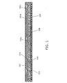
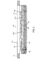
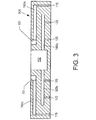
[適用例1]半導体プラズマ処理室内に処理ガスを供給するSi含有ガス分配部材を製造する方法であって、
該Si含有ガス分配部材の内部空洞構造に対応する形状に炭素部材を成形し、
Si含有材料で前記成形炭素部材の周囲に所定の厚さのシェルを形成するように、前記成形炭素部材上にSi含有材料を堆積させ、
前記Si含有シェルを、該Si含有ガス分配部材の構造に機械加工することであって、該機械加工により、該Si含有ガス分配部材の内部領域にある前記成形炭素部材の一部を露出させるようにガス入口および出口孔を形成し、
炭素と反応するガスによって炭素原子を解離させて、該Si含有ガス分配部材の内部領域から前記成形炭素部材を除去し、これにより、該Si含有ガス分配部材の内部領域に成形された内部空洞を残して、該Si含有ガス分配部材の内部領域から排除する
方法。
[適用例2]前記成形炭素部材上へのSi含有材料の堆積は、前記成形炭素部材を該成形炭素部材の第1の側で支持して、該成形炭素部材の第2の側にSi含有材料を堆積させることと、前記成形炭素部材を回転させて、Si含有材料が堆積された前記成形炭素部材の前記第2の側で支持し、前記成形炭素部材の前記第1の側にSi含有材料を堆積させることと、を含む適用例1に記載の方法。
[適用例3]前記成形炭素部材は、該Si含有ガス分配部材の内部空洞構造に対応する空間的関係で成形および配置される複数の分離された炭素要素を含み、該複数の分離された炭素要素は、複数の流体的に分離されたガスゾーンを該Si含有ガス分配部材内に形成するように配置され、
このとき、前記成形および配置された炭素要素上へのSi含有材料の堆積は、各炭素要素を第1の側で支持して、該成形および配置された炭素要素のそれぞれの第2の側にSi含有材料を堆積させることで、該成形および配置された炭素要素の前記第2の側に前記Si含有シェルの一部を形成することと、該成形および配置された炭素要素を回転させて、該成形および配置された炭素要素の前記Si含有シェルの前記一部が形成された前記第2の側で支持し、該成形および配置された炭素要素のそれぞれの第1の側にSi含有材料を堆積させることで、該成形および配置された炭素要素上に前記Si含有シェルを形成することと、を含む適用例1に記載の方法。
[適用例4]該Si含有ガス分配部材の内部で流体的に分離された前記ガスゾーンは、流体的に分離されたそれぞれのガスゾーンによって処理ガスの異なる放射状または環状の分布が可能となり得るように配置される適用例3に記載の方法。
[適用例5]2つの分離された炭素要素が、該Si含有ガス分配部材の内部で流体的に分離された2つのガスプレナムを含む内部空洞の対応する形状に成形される適用例3に記載の方法。
[適用例6]前記Si含有材料の堆積工程は、CVD法、PECVD法、またはコールドスプレー法により実施される適用例1に記載の方法。
[適用例7]前記成形炭素部材の除去は、アッシング処理を含む適用例1に記載の方法。
[適用例8]前記成形炭素部材の除去は、該Si含有ガス分配部材の内部領域から炭素を除去するために、前記Si含有コーティングされた炭素部材を酸素含有雰囲気中で加熱することを含む適用例1に記載の方法。
[適用例9]前記炭素部材の除去は、該Si含有ガス分配部材の内部領域から炭素を除去するために、前記Si含有コーティングされた炭素部材を水素含有雰囲気中で加熱することを含む適用例1に記載の方法。
[適用例10]各ガス入口および出口孔が、ドリル加工などの機械加工技術により作製される適用例1に記載の方法。
[適用例11]さらに各ガス入口および出口孔のレーザ孔あけによって、各ガス入口および出口孔の透過性が所定の透過率に調整される適用例10に記載の方法。
[適用例12]前記半導体プラズマ処理室は、プラズマエッチング室である適用例1に記載の方法。
[適用例13]該Si含有ガス分配部材は、バッキングプレート、熱制御プレート、またはガス分配プレートである適用例1に記載の方法。
[適用例14]前記成形炭素部材は黒鉛で形成される適用例1に記載の方法。
[適用例15]前記Si含有材料は、SiCである適用例1に記載の方法。
[適用例16]半導体プラズマ処理室用のシャワーヘッド電極アセンブリであって、
適用例1に記載の方法により製造されるSi含有ガス分配部材と、シリコンのシャワーヘッド電極とを含み、
前記Si含有ガス分配部材は、前記シリコンのシャワーヘッド電極のガス孔のパターンに一致するガス孔のパターンを有する
シャワーヘッド電極アセンブリ。
[適用例17]前記Si含有ガス分配部材は、ガス分配プレート、熱制御プレート、またはバッキングプレートである適用例16に記載のシャワーヘッド電極アセンブリ。
[適用例18]適用例16に記載のシャワーヘッド電極アセンブリを備えるプラズマ処理室内で半導体基板を処理する方法であって、
プラズマ処理装置に半導体基板を搬入して、該基板を基板サポート上で支持し、
前記Si含有ガス分配部材を通して、処理ガスを前記プラズマ処理室内に導入し、
前記処理ガスをプラズマ状態に励起し、
前記半導体基板を前記プラズマで処理する
方法。
[適用例19]前記処理は、前記基板上への導電材料または誘電材料の堆積を含む適用例18に記載の方法。
[適用例20]前記処理は、前記基板上の層をプラズマエッチングすることを含み、前記層は、金属、誘電体、またはフォトレジストである適用例18に記載の方法。
[適用例21]前記プラズマエッチングは、フッ化炭素および/またはハイドロフルオロカーボン・エッチングガスを用いて、誘電体材料に開口をエッチングすることを含む適用例20記載の方法。
Claims (15)
- 半導体プラズマ処理室内に処理ガスを供給するSi含有ガス分配部材を製造する方法であって、
該Si含有ガス分配部材の内部空洞構造に対応する形状に炭素部材を成形し、
前記成形された炭素部材である成形炭素部材の周囲に、Si含有材料が所定の厚さのシェルを形成するように、前記成形炭素部材上にSi含有材料を堆積させ、
Si含有の前記シェルを、該Si含有ガス分配部材の構造に機械加工することであって、該機械加工により、該Si含有ガス分配部材の内部領域にある前記成形炭素部材の一部を露出させるようにガス入口および出口孔を形成し、
炭素と反応するガスによって炭素原子を解離させて、該Si含有ガス分配部材の内部領域から前記成形炭素部材を除去し、これにより、該Si含有ガス分配部材の内部領域に成形された内部空洞を残して、該Si含有ガス分配部材の内部領域から排除する
方法。 - 前記成形炭素部材上へのSi含有材料の堆積は、前記成形炭素部材を該成形炭素部材の第1の側で支持して、該成形炭素部材の第2の側にSi含有材料を堆積させることと、前記成形炭素部材を回転させて、Si含有材料が堆積された前記成形炭素部材の前記第2の側で支持し、前記成形炭素部材の前記第1の側にSi含有材料を堆積させることと、を含む請求項1に記載の方法。
- 前記成形炭素部材は、該Si含有ガス分配部材の内部空洞構造に対応する空間的関係で成形および配置される複数の分離された炭素要素を含み、該複数の分離された炭素要素は、複数の流体的に分離されたガスゾーンを該Si含有ガス分配部材内に形成するように配置され、
このとき、前記成形および配置された炭素要素上へのSi含有材料の堆積は、各炭素要素を第1の側で支持して、該成形および配置された炭素要素のそれぞれの第2の側にSi含有材料を堆積させることで、該成形および配置された炭素要素の前記第2の側に前記Si含有シェルの一部を形成することと、該成形および配置された炭素要素を回転させて、該成形および配置された炭素要素の前記Si含有シェルの前記一部が形成された前記第2の側で支持し、該成形および配置された炭素要素のそれぞれの第1の側にSi含有材料を堆積させることで、該成形および配置された炭素要素上に前記Si含有シェルを形成することと、を含む請求項1に記載の方法。 - 該Si含有ガス分配部材の内部で流体的に分離された前記ガスゾーンは、流体的に分離されたそれぞれのガスゾーンによって処理ガスの異なる放射状または環状の分布が可能となり得るように配置される請求項3に記載の方法。
- 2つの分離された炭素要素が、該Si含有ガス分配部材の内部で流体的に分離された2つのガスプレナムを含む内部空洞の対応する形状に成形される請求項3に記載の方法。
- 前記Si含有材料の堆積工程は、CVD法、PECVD法、またはコールドスプレー法により実施される請求項1に記載の方法。
- 前記成形炭素部材の除去は、アッシング処理を含む請求項1に記載の方法。
- 前記成形炭素部材の除去は、該Si含有ガス分配部材の内部領域から炭素を除去するために、Si含有コーティングされた炭素部材を酸素含有雰囲気中で加熱することを含む請求項1に記載の方法。
- 前記炭素部材の除去は、該Si含有ガス分配部材の内部領域から炭素を除去するために、Si含有コーティングされた炭素部材を水素含有雰囲気中で加熱することを含む請求項1に記載の方法。
- 各ガス入口および出口孔が、機械加工技術により作製される請求項1に記載の方法。
- さらに各ガス入口および出口孔のレーザ孔あけによって、各ガス入口および出口孔の透過性が所定の透過率に調整される請求項10に記載の方法。
- 前記半導体プラズマ処理室は、プラズマエッチング室である請求項1に記載の方法。
- 該Si含有ガス分配部材は、バッキングプレート、熱制御プレート、またはガス分配プレートである請求項1に記載の方法。
- 前記成形炭素部材は黒鉛で形成される請求項1に記載の方法。
- 前記Si含有材料は、SiCである請求項1に記載の方法。
Applications Claiming Priority (2)
| Application Number | Priority Date | Filing Date | Title |
|---|---|---|---|
| US13/766,096 US8883029B2 (en) | 2013-02-13 | 2013-02-13 | Method of making a gas distribution member for a plasma processing chamber |
| US13/766,096 | 2013-02-13 |
Publications (3)
| Publication Number | Publication Date |
|---|---|
| JP2014160819A JP2014160819A (ja) | 2014-09-04 |
| JP2014160819A5 JP2014160819A5 (ja) | 2017-03-09 |
| JP6335538B2 true JP6335538B2 (ja) | 2018-05-30 |
Family
ID=51297720
Family Applications (1)
| Application Number | Title | Priority Date | Filing Date |
|---|---|---|---|
| JP2014025393A Active JP6335538B2 (ja) | 2013-02-13 | 2014-02-13 | プラズマ処理室用のガス分配部材を製造する方法 |
Country Status (4)
| Country | Link |
|---|---|
| US (2) | US8883029B2 (ja) |
| JP (1) | JP6335538B2 (ja) |
| KR (1) | KR20140102154A (ja) |
| TW (1) | TWI662148B (ja) |
Families Citing this family (17)
| Publication number | Priority date | Publication date | Assignee | Title |
|---|---|---|---|---|
| US8883029B2 (en) * | 2013-02-13 | 2014-11-11 | Lam Research Corporation | Method of making a gas distribution member for a plasma processing chamber |
| US20140315392A1 (en) * | 2013-04-22 | 2014-10-23 | Lam Research Corporation | Cold spray barrier coated component of a plasma processing chamber and method of manufacture thereof |
| US9580360B2 (en) | 2014-04-07 | 2017-02-28 | Lam Research Corporation | Monolithic ceramic component of gas delivery system and method of making and use thereof |
| JP6375163B2 (ja) * | 2014-07-11 | 2018-08-15 | 東京エレクトロン株式会社 | プラズマ処理装置および上部電極アセンブリ |
| US9837254B2 (en) * | 2014-08-12 | 2017-12-05 | Lam Research Corporation | Differentially pumped reactive gas injector |
| US10825652B2 (en) | 2014-08-29 | 2020-11-03 | Lam Research Corporation | Ion beam etch without need for wafer tilt or rotation |
| US9406535B2 (en) | 2014-08-29 | 2016-08-02 | Lam Research Corporation | Ion injector and lens system for ion beam milling |
| US9536748B2 (en) | 2014-10-21 | 2017-01-03 | Lam Research Corporation | Use of ion beam etching to generate gate-all-around structure |
| CN106783669B (zh) * | 2015-11-25 | 2019-04-12 | 无锡华瑛微电子技术有限公司 | 半导体处理装置及方法 |
| US10203604B2 (en) | 2015-11-30 | 2019-02-12 | Applied Materials, Inc. | Method and apparatus for post exposure processing of photoresist wafers |
| US9779955B2 (en) | 2016-02-25 | 2017-10-03 | Lam Research Corporation | Ion beam etching utilizing cryogenic wafer temperatures |
| US9958782B2 (en) | 2016-06-29 | 2018-05-01 | Applied Materials, Inc. | Apparatus for post exposure bake |
| US10954596B2 (en) * | 2016-12-08 | 2021-03-23 | Applied Materials, Inc. | Temporal atomic layer deposition process chamber |
| US11881384B2 (en) * | 2019-09-27 | 2024-01-23 | Applied Materials, Inc. | Monolithic modular microwave source with integrated process gas distribution |
| CN113025998B (zh) * | 2019-12-24 | 2023-09-01 | 广东众元半导体科技有限公司 | 一种金刚石薄膜微波等离子体化学气相沉积使用的基片台 |
| US11694908B2 (en) * | 2020-10-22 | 2023-07-04 | Applied Materials, Inc. | Gasbox for semiconductor processing chamber |
| US11776793B2 (en) * | 2020-11-13 | 2023-10-03 | Applied Materials, Inc. | Plasma source with ceramic electrode plate |
Family Cites Families (39)
| Publication number | Priority date | Publication date | Assignee | Title |
|---|---|---|---|---|
| JPH03162593A (ja) * | 1989-11-21 | 1991-07-12 | Hitachi Chem Co Ltd | プラズマエツチング用電極板及びその製造法 |
| JP3897393B2 (ja) * | 1997-04-14 | 2007-03-22 | 東芝セラミックス株式会社 | 高純度炭化珪素質半導体処理部材の製造方法 |
| JP3478703B2 (ja) * | 1997-05-15 | 2003-12-15 | 信越化学工業株式会社 | 炭化けい素電極板の製造方法 |
| JPH11104950A (ja) * | 1997-10-03 | 1999-04-20 | Shin Etsu Chem Co Ltd | 電極板及びその製造方法 |
| US6073577A (en) | 1998-06-30 | 2000-06-13 | Lam Research Corporation | Electrode for plasma processes and method for manufacture and use thereof |
| FR2790953B1 (fr) * | 1999-03-19 | 2002-08-09 | Oreal | Composition a phase aqueuse continue renfermant de l'acide l-2-oxothiazolidine 4-carboxylique |
| KR100806097B1 (ko) * | 1999-09-30 | 2008-02-21 | 램 리써치 코포레이션 | 예비 처리된 가스 분배판 |
| US6444040B1 (en) * | 2000-05-05 | 2002-09-03 | Applied Materials Inc. | Gas distribution plate |
| US6630756B2 (en) * | 2001-07-12 | 2003-10-07 | Generac Power Systems, Inc. | Air flow arrangement for generator enclosure |
| JP2003059903A (ja) * | 2001-08-10 | 2003-02-28 | Ibiden Co Ltd | プラズマエッチング装置のガス吹き出し板及びその製造方法 |
| CN100442429C (zh) * | 2002-05-23 | 2008-12-10 | 蓝姆研究公司 | 用于半导体处理等离子反应器的多部分电极以及替换多部分电极的一部分的方法 |
| US7267741B2 (en) * | 2003-11-14 | 2007-09-11 | Lam Research Corporation | Silicon carbide components of semiconductor substrate processing apparatuses treated to remove free-carbon |
| US7645341B2 (en) * | 2003-12-23 | 2010-01-12 | Lam Research Corporation | Showerhead electrode assembly for plasma processing apparatuses |
| JP2005285845A (ja) * | 2004-03-26 | 2005-10-13 | Ibiden Co Ltd | プラズマエッチング装置のガス吹き出し板 |
| JP2005285846A (ja) * | 2004-03-26 | 2005-10-13 | Ibiden Co Ltd | プラズマエッチング装置のガス吹き出し板 |
| US7712434B2 (en) | 2004-04-30 | 2010-05-11 | Lam Research Corporation | Apparatus including showerhead electrode and heater for plasma processing |
| US8317968B2 (en) * | 2004-04-30 | 2012-11-27 | Lam Research Corporation | Apparatus including gas distribution member supplying process gas and radio frequency (RF) power for plasma processing |
| US7480974B2 (en) | 2005-02-15 | 2009-01-27 | Lam Research Corporation | Methods of making gas distribution members for plasma processing apparatuses |
| US8679252B2 (en) * | 2005-09-23 | 2014-03-25 | Lam Research Corporation | Actively heated aluminum baffle component having improved particle performance and methods of use and manufacture thereof |
| US7854820B2 (en) * | 2006-10-16 | 2010-12-21 | Lam Research Corporation | Upper electrode backing member with particle reducing features |
| US20080087641A1 (en) * | 2006-10-16 | 2008-04-17 | Lam Research Corporation | Components for a plasma processing apparatus |
| US8702866B2 (en) * | 2006-12-18 | 2014-04-22 | Lam Research Corporation | Showerhead electrode assembly with gas flow modification for extended electrode life |
| US8069817B2 (en) | 2007-03-30 | 2011-12-06 | Lam Research Corporation | Showerhead electrodes and showerhead electrode assemblies having low-particle performance for semiconductor material processing apparatuses |
| CN101889329B (zh) * | 2007-10-31 | 2012-07-04 | 朗姆研究公司 | 长寿命可消耗氮化硅-二氧化硅等离子处理部件 |
| JP5265700B2 (ja) * | 2007-12-19 | 2013-08-14 | ラム リサーチ コーポレーション | プラズマ処理装置用の複合シャワーヘッド電極組立体 |
| US8161906B2 (en) | 2008-07-07 | 2012-04-24 | Lam Research Corporation | Clamped showerhead electrode assembly |
| US8221582B2 (en) | 2008-07-07 | 2012-07-17 | Lam Research Corporation | Clamped monolithic showerhead electrode |
| US8449679B2 (en) * | 2008-08-15 | 2013-05-28 | Lam Research Corporation | Temperature controlled hot edge ring assembly |
| US8147648B2 (en) * | 2008-08-15 | 2012-04-03 | Lam Research Corporation | Composite showerhead electrode assembly for a plasma processing apparatus |
| US8272346B2 (en) * | 2009-04-10 | 2012-09-25 | Lam Research Corporation | Gasket with positioning feature for clamped monolithic showerhead electrode |
| US20110002103A1 (en) * | 2009-07-01 | 2011-01-06 | Wen-Yi Lee | Interlocking Structure For Memory Heat Sink |
| SG169960A1 (en) * | 2009-09-18 | 2011-04-29 | Lam Res Corp | Clamped monolithic showerhead electrode |
| JP3160877U (ja) * | 2009-10-13 | 2010-07-15 | ラム リサーチ コーポレーションLam Research Corporation | シャワーヘッド電極アセンブリの端部クランプ留めおよび機械固定される内側電極 |
| US8470127B2 (en) | 2011-01-06 | 2013-06-25 | Lam Research Corporation | Cam-locked showerhead electrode and assembly |
| JP5808697B2 (ja) * | 2012-03-01 | 2015-11-10 | 株式会社日立ハイテクノロジーズ | ドライエッチング装置及びドライエッチング方法 |
| US9058960B2 (en) * | 2012-05-09 | 2015-06-16 | Lam Research Corporation | Compression member for use in showerhead electrode assembly |
| US8975817B2 (en) * | 2012-10-17 | 2015-03-10 | Lam Research Corporation | Pressure controlled heat pipe temperature control plate |
| US8883029B2 (en) * | 2013-02-13 | 2014-11-11 | Lam Research Corporation | Method of making a gas distribution member for a plasma processing chamber |
| US9580360B2 (en) * | 2014-04-07 | 2017-02-28 | Lam Research Corporation | Monolithic ceramic component of gas delivery system and method of making and use thereof |
-
2013
- 2013-02-13 US US13/766,096 patent/US8883029B2/en not_active Expired - Fee Related
-
2014
- 2014-02-13 TW TW103104796A patent/TWI662148B/zh active
- 2014-02-13 KR KR1020140016848A patent/KR20140102154A/ko not_active Application Discontinuation
- 2014-02-13 JP JP2014025393A patent/JP6335538B2/ja active Active
- 2014-10-09 US US14/510,681 patent/US20150024582A1/en not_active Abandoned
Also Published As
| Publication number | Publication date |
|---|---|
| TW201443273A (zh) | 2014-11-16 |
| KR20140102154A (ko) | 2014-08-21 |
| US20140227866A1 (en) | 2014-08-14 |
| US20150024582A1 (en) | 2015-01-22 |
| JP2014160819A (ja) | 2014-09-04 |
| TWI662148B (zh) | 2019-06-11 |
| US8883029B2 (en) | 2014-11-11 |
Similar Documents
| Publication | Publication Date | Title |
|---|---|---|
| JP6335538B2 (ja) | プラズマ処理室用のガス分配部材を製造する方法 | |
| JP7393501B2 (ja) | 前駆体の流れを改善する半導体処理チャンバ | |
| TWI670783B (zh) | 增進製程均勻性的方法及系統 | |
| WO2019164761A1 (en) | Multi-plate electrostatic chucks with ceramic baseplates | |
| US11915950B2 (en) | Multi-zone semiconductor substrate supports | |
| US20080023029A1 (en) | Silicon carbide components of semiconductor substrate processing apparatuses treated to remove free-carbon | |
| TWI796249B (zh) | 可運動的邊緣環設計 | |
| JP2014160819A5 (ja) | ||
| US20230093478A1 (en) | Semiconductor chamber components with high-performance coating | |
| TWI827654B (zh) | 用於基板處理系統之侷限環與在基板處理系統中使用侷限環的方法 | |
| US20230290616A1 (en) | Semiconductor chamber components with multi-layer coating | |
| US20220084845A1 (en) | High conductance process kit | |
| TW202336270A (zh) | 具有背側泵送的熱處理腔室蓋 | |
| KR20180025598A (ko) | 기판 지지 유닛 및 이를 가지는 기판 처리 장치 |
Legal Events
| Date | Code | Title | Description |
|---|---|---|---|
| A521 | Request for written amendment filed |
Free format text: JAPANESE INTERMEDIATE CODE: A523 Effective date: 20170206 |
|
| A621 | Written request for application examination |
Free format text: JAPANESE INTERMEDIATE CODE: A621 Effective date: 20170206 |
|
| A977 | Report on retrieval |
Free format text: JAPANESE INTERMEDIATE CODE: A971007 Effective date: 20171127 |
|
| A131 | Notification of reasons for refusal |
Free format text: JAPANESE INTERMEDIATE CODE: A131 Effective date: 20171219 |
|
| A521 | Request for written amendment filed |
Free format text: JAPANESE INTERMEDIATE CODE: A523 Effective date: 20180316 |
|
| TRDD | Decision of grant or rejection written | ||
| A01 | Written decision to grant a patent or to grant a registration (utility model) |
Free format text: JAPANESE INTERMEDIATE CODE: A01 Effective date: 20180403 |
|
| A61 | First payment of annual fees (during grant procedure) |
Free format text: JAPANESE INTERMEDIATE CODE: A61 Effective date: 20180501 |
|
| R150 | Certificate of patent or registration of utility model |
Ref document number: 6335538 Country of ref document: JP Free format text: JAPANESE INTERMEDIATE CODE: R150 |
|
| R250 | Receipt of annual fees |
Free format text: JAPANESE INTERMEDIATE CODE: R250 |
|
| R250 | Receipt of annual fees |
Free format text: JAPANESE INTERMEDIATE CODE: R250 |
|
| R250 | Receipt of annual fees |
Free format text: JAPANESE INTERMEDIATE CODE: R250 |
|
| R250 | Receipt of annual fees |
Free format text: JAPANESE INTERMEDIATE CODE: R250 |