JP6315892B2 - 液晶表示パネル - Google Patents
液晶表示パネル Download PDFInfo
- Publication number
- JP6315892B2 JP6315892B2 JP2013102687A JP2013102687A JP6315892B2 JP 6315892 B2 JP6315892 B2 JP 6315892B2 JP 2013102687 A JP2013102687 A JP 2013102687A JP 2013102687 A JP2013102687 A JP 2013102687A JP 6315892 B2 JP6315892 B2 JP 6315892B2
- Authority
- JP
- Japan
- Prior art keywords
- liquid crystal
- conductive layer
- crystal display
- tft array
- gate
- Prior art date
- Legal status (The legal status is an assumption and is not a legal conclusion. Google has not performed a legal analysis and makes no representation as to the accuracy of the status listed.)
- Active
Links
- 239000010410 layer Substances 0.000 claims description 155
- 239000004973 liquid crystal related substance Substances 0.000 claims description 141
- 239000000758 substrate Substances 0.000 claims description 134
- 239000010408 film Substances 0.000 claims description 46
- 239000003566 sealing material Substances 0.000 claims description 36
- 230000005684 electric field Effects 0.000 claims description 34
- 239000011159 matrix material Substances 0.000 claims description 16
- 239000011347 resin Substances 0.000 claims description 13
- 229920005989 resin Polymers 0.000 claims description 13
- 229910052751 metal Inorganic materials 0.000 claims description 10
- 239000002184 metal Substances 0.000 claims description 10
- 239000004020 conductor Substances 0.000 claims description 8
- 239000002245 particle Substances 0.000 claims description 4
- 239000010409 thin film Substances 0.000 claims description 3
- 230000004888 barrier function Effects 0.000 claims description 2
- 239000000565 sealant Substances 0.000 claims 1
- 238000007689 inspection Methods 0.000 description 12
- 239000000463 material Substances 0.000 description 11
- 230000000694 effects Effects 0.000 description 8
- 239000011521 glass Substances 0.000 description 8
- 241000519995 Stachys sylvatica Species 0.000 description 5
- 238000004519 manufacturing process Methods 0.000 description 5
- 230000007246 mechanism Effects 0.000 description 5
- 238000000034 method Methods 0.000 description 5
- 230000006872 improvement Effects 0.000 description 3
- 239000007769 metal material Substances 0.000 description 3
- BQCADISMDOOEFD-UHFFFAOYSA-N Silver Chemical compound [Ag] BQCADISMDOOEFD-UHFFFAOYSA-N 0.000 description 2
- 230000007547 defect Effects 0.000 description 2
- 239000011888 foil Substances 0.000 description 2
- 230000002093 peripheral effect Effects 0.000 description 2
- 239000000047 product Substances 0.000 description 2
- 230000007261 regionalization Effects 0.000 description 2
- 238000007789 sealing Methods 0.000 description 2
- 229910052709 silver Inorganic materials 0.000 description 2
- 239000004332 silver Substances 0.000 description 2
- OKTJSMMVPCPJKN-UHFFFAOYSA-N Carbon Chemical compound [C] OKTJSMMVPCPJKN-UHFFFAOYSA-N 0.000 description 1
- RYGMFSIKBFXOCR-UHFFFAOYSA-N Copper Chemical compound [Cu] RYGMFSIKBFXOCR-UHFFFAOYSA-N 0.000 description 1
- 239000004820 Pressure-sensitive adhesive Substances 0.000 description 1
- RTAQQCXQSZGOHL-UHFFFAOYSA-N Titanium Chemical compound [Ti] RTAQQCXQSZGOHL-UHFFFAOYSA-N 0.000 description 1
- WGLPBDUCMAPZCE-UHFFFAOYSA-N Trioxochromium Chemical compound O=[Cr](=O)=O WGLPBDUCMAPZCE-UHFFFAOYSA-N 0.000 description 1
- 230000009471 action Effects 0.000 description 1
- 239000000853 adhesive Substances 0.000 description 1
- 230000001070 adhesive effect Effects 0.000 description 1
- 239000012790 adhesive layer Substances 0.000 description 1
- 230000002411 adverse Effects 0.000 description 1
- 229910052799 carbon Inorganic materials 0.000 description 1
- 229910000423 chromium oxide Inorganic materials 0.000 description 1
- 239000013065 commercial product Substances 0.000 description 1
- 230000005611 electricity Effects 0.000 description 1
- AMGQUBHHOARCQH-UHFFFAOYSA-N indium;oxotin Chemical compound [In].[Sn]=O AMGQUBHHOARCQH-UHFFFAOYSA-N 0.000 description 1
- 239000011229 interlayer Substances 0.000 description 1
- 230000003287 optical effect Effects 0.000 description 1
- 239000000049 pigment Substances 0.000 description 1
- 230000008569 process Effects 0.000 description 1
- 230000009467 reduction Effects 0.000 description 1
- 230000002040 relaxant effect Effects 0.000 description 1
- 239000002356 single layer Substances 0.000 description 1
- 125000006850 spacer group Chemical group 0.000 description 1
- 230000003068 static effect Effects 0.000 description 1
- 230000001629 suppression Effects 0.000 description 1
- 239000010936 titanium Substances 0.000 description 1
- 229910052719 titanium Inorganic materials 0.000 description 1
Images


Classifications
-
- G—PHYSICS
- G02—OPTICS
- G02F—OPTICAL DEVICES OR ARRANGEMENTS FOR THE CONTROL OF LIGHT BY MODIFICATION OF THE OPTICAL PROPERTIES OF THE MEDIA OF THE ELEMENTS INVOLVED THEREIN; NON-LINEAR OPTICS; FREQUENCY-CHANGING OF LIGHT; OPTICAL LOGIC ELEMENTS; OPTICAL ANALOGUE/DIGITAL CONVERTERS
- G02F1/00—Devices or arrangements for the control of the intensity, colour, phase, polarisation or direction of light arriving from an independent light source, e.g. switching, gating or modulating; Non-linear optics
- G02F1/01—Devices or arrangements for the control of the intensity, colour, phase, polarisation or direction of light arriving from an independent light source, e.g. switching, gating or modulating; Non-linear optics for the control of the intensity, phase, polarisation or colour
- G02F1/13—Devices or arrangements for the control of the intensity, colour, phase, polarisation or direction of light arriving from an independent light source, e.g. switching, gating or modulating; Non-linear optics for the control of the intensity, phase, polarisation or colour based on liquid crystals, e.g. single liquid crystal display cells
- G02F1/133—Constructional arrangements; Operation of liquid crystal cells; Circuit arrangements
- G02F1/1333—Constructional arrangements; Manufacturing methods
- G02F1/1343—Electrodes
- G02F1/134309—Electrodes characterised by their geometrical arrangement
- G02F1/134363—Electrodes characterised by their geometrical arrangement for applying an electric field parallel to the substrate, i.e. in-plane switching [IPS]
-
- G—PHYSICS
- G02—OPTICS
- G02F—OPTICAL DEVICES OR ARRANGEMENTS FOR THE CONTROL OF LIGHT BY MODIFICATION OF THE OPTICAL PROPERTIES OF THE MEDIA OF THE ELEMENTS INVOLVED THEREIN; NON-LINEAR OPTICS; FREQUENCY-CHANGING OF LIGHT; OPTICAL LOGIC ELEMENTS; OPTICAL ANALOGUE/DIGITAL CONVERTERS
- G02F2202/00—Materials and properties
- G02F2202/22—Antistatic materials or arrangements
Description
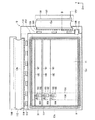
図1および図2は、本発明の実施の形態1に係る液晶表示装置を構成する液晶パネルの概略図である。図1は、液晶パネルの全体構成を示した平面図であり、図2は、図1におけるA−B線に沿った断面図である。本実施の形態では、各画素のスイッチング素子としてTFTを用いた横電界方式の液晶パネル、特にFFS方式の液晶パネルに本発明を適用した例を説明する。
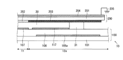
実施の形態1では、TFTアレイ基板100の最表面を覆う導電層117を、液晶層30内(シール材31よりも内側)のみに配置したが、その配置場所はこの限りではない。
実施の形態1では、TFTアレイ基板100の最表面を覆う導電層117を、表示領域11に設けられる共通電極103または画素電極102と同じ透明導電膜を用いて形成したが、導電層117の材料はこれに限られない。
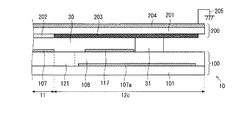
図7および図8は、実施の形態4に係る液晶パネル10の額縁領域12近傍の断面図であり、図7は額縁領域12aの近傍、図8は額縁領域12cの近傍をそれぞれ示している。実施の形態4の液晶パネル10の構成は、実施の形態1とほぼ同様であるが、対向基板200のシールド導電層204の接地構造(図3および図4の接地構造205)を省略している。
Claims (9)
- 各画素のTFT(Thin Film Transistor)が配設されたTFTアレイ基板と、
前記TFTアレイ基板に対向配置され、外側の面にシールド導電層を有する対向基板と、
前記TFTアレイ基板と前記対向基板との間に挟持された液晶層と、
を備える横電界方式の液晶表示パネルであって、
前記TFTアレイ基板は、
前記TFTのゲート電極に接続したゲート配線と、
前記ゲート配線を表示領域より外側の額縁領域へ引き出すゲート引き出し配線と、
前記ゲート引き出し配線が配置されない辺を含む全ての辺の前記額縁領域において、前記TFTアレイ基板における前記ゲート引き出し配線を覆うように形成された絶縁膜の表面を覆って配置されるとともに、前記液晶層と前記絶縁膜の表面との境界面に配置された導電層と、を備え、
前記液晶表示パネルは、
前記額縁領域において前記TFTアレイ基板と前記対向基板の間に形成され、前記液晶層を封止するシール材をさらに備え、
前記導電層は、前記シール材と表示領域との間に形成されており、
前記シールド導電層は、特定の電位に固定されないフローティング状態である
ことを特徴とする液晶表示パネル。 - 前記導電層には、各画素の共通電極の電位である共通電位が供給される
請求項1記載の液晶表示パネル。 - 前記導電層は、各画素の画素電極または共通電極と同じ透明導電膜により形成されている
請求項1または請求項2記載の液晶表示パネル。 - 前記導電層は、金属膜により形成されている
請求項1または請求項2記載の液晶表示パネル。 - 前記対向基板は、前記液晶層側の面に、黒色粒子を分散させた樹脂により形成されたブラックマトリクスをさらに備える
請求項1から請求項4のいずれか一項記載の液晶表示パネル。 - 前記シールド導電層は、視差バリアを構成する遮光性導電膜である
請求項1記載の液晶表示パネル。 - 前記シールド導電層は、前記対向基板の前面側に配置されるタッチパネルと前記対向基板との間にノイズシールドとして設けられた透明導電膜である
請求項1記載の液晶表示パネル。 - 前記導電層の外側端部は、前記シール材に接触するように前記シール材と重複しており、
前記シール材の表面の抵抗値は、前記液晶層の抵抗値よりも小さい
請求項1から請求項7のいずれか一項記載の液晶表示パネル。 - 前記導電層の外側端部は、前記シール材に接触するように前記シール材と重複しており、
前記シール材は、導電性材料により構成されている
請求項1から請求項7のいずれか一項記載の液晶表示パネル。
Priority Applications (2)
| Application Number | Priority Date | Filing Date | Title |
|---|---|---|---|
| JP2013102687A JP6315892B2 (ja) | 2013-05-15 | 2013-05-15 | 液晶表示パネル |
| US14/268,268 US20140340605A1 (en) | 2013-05-15 | 2014-05-02 | Liquid crystal display panel |
Applications Claiming Priority (1)
| Application Number | Priority Date | Filing Date | Title |
|---|---|---|---|
| JP2013102687A JP6315892B2 (ja) | 2013-05-15 | 2013-05-15 | 液晶表示パネル |
Publications (3)
| Publication Number | Publication Date |
|---|---|
| JP2014224840A JP2014224840A (ja) | 2014-12-04 |
| JP2014224840A5 JP2014224840A5 (ja) | 2016-06-30 |
| JP6315892B2 true JP6315892B2 (ja) | 2018-04-25 |
Family
ID=51895520
Family Applications (1)
| Application Number | Title | Priority Date | Filing Date |
|---|---|---|---|
| JP2013102687A Active JP6315892B2 (ja) | 2013-05-15 | 2013-05-15 | 液晶表示パネル |
Country Status (2)
| Country | Link |
|---|---|
| US (1) | US20140340605A1 (ja) |
| JP (1) | JP6315892B2 (ja) |
Families Citing this family (8)
| Publication number | Priority date | Publication date | Assignee | Title |
|---|---|---|---|---|
| CN103926729B (zh) * | 2013-12-31 | 2017-12-22 | 上海天马微电子有限公司 | 一种阵列基板、彩膜基板、触控显示装置及其驱动方法 |
| CN104880869A (zh) * | 2015-06-19 | 2015-09-02 | 京东方科技集团股份有限公司 | 显示面板及其制作方法、显示装置 |
| CN105182599B (zh) * | 2015-10-23 | 2018-12-18 | 京东方科技集团股份有限公司 | 显示面板和显示装置 |
| CN105677098B (zh) * | 2016-01-05 | 2018-09-11 | 京东方科技集团股份有限公司 | 一种触摸屏和触控设备 |
| CN105552028A (zh) * | 2016-02-18 | 2016-05-04 | 京东方科技集团股份有限公司 | 阵列基板及其制作方法、显示面板及显示装置 |
| CN108700787A (zh) | 2016-03-01 | 2018-10-23 | 夏普株式会社 | 显示装置及显示装置的检查方法 |
| CN113325641B (zh) * | 2018-06-29 | 2022-12-30 | 上海中航光电子有限公司 | 一种阵列基板、显示面板及显示装置 |
| CN114253035A (zh) * | 2020-09-23 | 2022-03-29 | 京东方科技集团股份有限公司 | 显示装置和阵列基板 |
Family Cites Families (16)
| Publication number | Priority date | Publication date | Assignee | Title |
|---|---|---|---|---|
| JPH0827458B2 (ja) * | 1986-08-26 | 1996-03-21 | オプトレツクス株式会社 | 液晶表示素子 |
| JP2006323097A (ja) * | 2005-05-18 | 2006-11-30 | Toshiba Matsushita Display Technology Co Ltd | 液晶表示装置 |
| US20070002192A1 (en) * | 2005-06-29 | 2007-01-04 | Casio Computer Co., Ltd. | Liquid crystal display apparatus including touch panel |
| JP2007052183A (ja) * | 2005-08-17 | 2007-03-01 | Nec Lcd Technologies Ltd | タッチパネル搭載液晶表示装置及びその製造方法 |
| US8395738B2 (en) * | 2007-10-17 | 2013-03-12 | Japan Display Central Inc. | Liquid crystal display device |
| JP4678031B2 (ja) * | 2008-01-11 | 2011-04-27 | ソニー株式会社 | 液晶装置および電子機器 |
| US8310609B2 (en) * | 2008-09-30 | 2012-11-13 | Sony Corporation | Liquid crystal device, electronic apparatus, and method of manufacturing liquid crystal device |
| JP5294883B2 (ja) * | 2009-01-05 | 2013-09-18 | 株式会社ジャパンディスプレイウェスト | 液晶表示装置および電子機器 |
| JP5238571B2 (ja) * | 2009-03-25 | 2013-07-17 | 株式会社東芝 | 液晶表示装置 |
| JP5015274B2 (ja) * | 2010-01-13 | 2012-08-29 | シャープ株式会社 | 表示パネルおよび表示装置 |
| JP5453146B2 (ja) * | 2010-03-16 | 2014-03-26 | 株式会社ジャパンディスプレイ | 表示装置 |
| US20130128192A1 (en) * | 2010-08-02 | 2013-05-23 | Sharp Kabushiki Kaisha | Liquid crystal display device and manufacturing method for same |
| JP5756860B2 (ja) * | 2011-08-10 | 2015-07-29 | シャープ株式会社 | 液晶ディスプレイ |
| JP5520899B2 (ja) * | 2011-08-23 | 2014-06-11 | 株式会社ジャパンディスプレイ | 液晶表示装置 |
| JP2013064800A (ja) * | 2011-09-15 | 2013-04-11 | Japan Display Central Co Ltd | 液晶表示装置 |
| KR101945866B1 (ko) * | 2012-03-19 | 2019-02-11 | 삼성디스플레이 주식회사 | 차폐 도전체를 가지는 액정 표시 장치 |
-
2013
- 2013-05-15 JP JP2013102687A patent/JP6315892B2/ja active Active
-
2014
- 2014-05-02 US US14/268,268 patent/US20140340605A1/en not_active Abandoned
Also Published As
| Publication number | Publication date |
|---|---|
| US20140340605A1 (en) | 2014-11-20 |
| JP2014224840A (ja) | 2014-12-04 |
Similar Documents
| Publication | Publication Date | Title |
|---|---|---|
| JP6315892B2 (ja) | 液晶表示パネル | |
| TWI629623B (zh) | Display device | |
| US11867997B2 (en) | Liquid crystal display device | |
| JP5013554B2 (ja) | 液晶表示装置 | |
| US10324346B2 (en) | Display device | |
| JP5585127B2 (ja) | アレイ基板、および液晶表示装置 | |
| WO2011096123A1 (ja) | 液晶表示装置 | |
| JP2009086184A (ja) | タッチパネル付き液晶表示装置 | |
| TWI481925B (zh) | 顯示裝置,其製造方法,及電子裝置 | |
| JP2015084017A (ja) | 液晶表示装置 | |
| JP6436666B2 (ja) | 液晶表示装置 | |
| JP5736895B2 (ja) | 横電界方式の液晶表示装置 | |
| JP2017111396A (ja) | 表示装置 | |
| WO2017022609A1 (ja) | 表示パネル | |
| JP2017015923A (ja) | 液晶表示装置 | |
| JP2008158392A (ja) | 液晶表示装置 | |
| JP5207422B2 (ja) | 液晶表示装置 | |
| JP6037753B2 (ja) | 液晶表示装置 | |
| JP5247615B2 (ja) | 横電界方式の液晶表示装置 | |
| US20220221763A1 (en) | Liquid crystal display device | |
| US20200387024A1 (en) | Display panel and display device | |
| JP2010217636A (ja) | 電気光学装置、電気光学装置の製造方法及び電子機器 | |
| JP7094810B2 (ja) | 表示装置 | |
| JP2011002609A (ja) | 横電界方式の液晶表示装置 | |
| JP5392702B2 (ja) | 液晶表示装置および電子機器 |
Legal Events
| Date | Code | Title | Description |
|---|---|---|---|
| A521 | Request for written amendment filed |
Free format text: JAPANESE INTERMEDIATE CODE: A523 Effective date: 20160511 |
|
| A621 | Written request for application examination |
Free format text: JAPANESE INTERMEDIATE CODE: A621 Effective date: 20160511 |
|
| A977 | Report on retrieval |
Free format text: JAPANESE INTERMEDIATE CODE: A971007 Effective date: 20170316 |
|
| A131 | Notification of reasons for refusal |
Free format text: JAPANESE INTERMEDIATE CODE: A131 Effective date: 20170328 |
|
| A521 | Request for written amendment filed |
Free format text: JAPANESE INTERMEDIATE CODE: A523 Effective date: 20170417 |
|
| A131 | Notification of reasons for refusal |
Free format text: JAPANESE INTERMEDIATE CODE: A131 Effective date: 20170905 |
|
| A521 | Request for written amendment filed |
Free format text: JAPANESE INTERMEDIATE CODE: A523 Effective date: 20171020 |
|
| TRDD | Decision of grant or rejection written | ||
| A01 | Written decision to grant a patent or to grant a registration (utility model) |
Free format text: JAPANESE INTERMEDIATE CODE: A01 Effective date: 20180227 |
|
| A61 | First payment of annual fees (during grant procedure) |
Free format text: JAPANESE INTERMEDIATE CODE: A61 Effective date: 20180327 |
|
| R150 | Certificate of patent or registration of utility model |
Ref document number: 6315892 Country of ref document: JP Free format text: JAPANESE INTERMEDIATE CODE: R150 |
|
| R250 | Receipt of annual fees |
Free format text: JAPANESE INTERMEDIATE CODE: R250 |
|
| R250 | Receipt of annual fees |
Free format text: JAPANESE INTERMEDIATE CODE: R250 |
|
| R250 | Receipt of annual fees |
Free format text: JAPANESE INTERMEDIATE CODE: R250 |
|
| R250 | Receipt of annual fees |
Free format text: JAPANESE INTERMEDIATE CODE: R250 |