JP6258576B2 - 光電素子の製造方法 - Google Patents
光電素子の製造方法 Download PDFInfo
- Publication number
- JP6258576B2 JP6258576B2 JP2012219627A JP2012219627A JP6258576B2 JP 6258576 B2 JP6258576 B2 JP 6258576B2 JP 2012219627 A JP2012219627 A JP 2012219627A JP 2012219627 A JP2012219627 A JP 2012219627A JP 6258576 B2 JP6258576 B2 JP 6258576B2
- Authority
- JP
- Japan
- Prior art keywords
- doping
- semiconductor substrate
- material layer
- layer
- doping material
- Prior art date
- Legal status (The legal status is an assumption and is not a legal conclusion. Google has not performed a legal analysis and makes no representation as to the accuracy of the status listed.)
- Active
Links
- 238000000034 method Methods 0.000 title claims description 71
- 238000004519 manufacturing process Methods 0.000 title claims description 40
- 239000000758 substrate Substances 0.000 claims description 120
- 239000004065 semiconductor Substances 0.000 claims description 119
- 239000000463 material Substances 0.000 claims description 96
- 238000009792 diffusion process Methods 0.000 claims description 63
- 239000002019 doping agent Substances 0.000 claims description 38
- RLOWWWKZYUNIDI-UHFFFAOYSA-N phosphinic chloride Chemical compound ClP=O RLOWWWKZYUNIDI-UHFFFAOYSA-N 0.000 claims description 28
- 230000008021 deposition Effects 0.000 claims description 27
- 238000010438 heat treatment Methods 0.000 claims description 22
- 238000005530 etching Methods 0.000 claims description 13
- 239000012159 carrier gas Substances 0.000 claims description 12
- VYPSYNLAJGMNEJ-UHFFFAOYSA-N Silicium dioxide Chemical compound O=[Si]=O VYPSYNLAJGMNEJ-UHFFFAOYSA-N 0.000 claims description 8
- 229910052814 silicon oxide Inorganic materials 0.000 claims description 8
- 239000003929 acidic solution Substances 0.000 claims description 3
- 238000013459 approach Methods 0.000 claims description 2
- 239000010410 layer Substances 0.000 description 186
- 238000005137 deposition process Methods 0.000 description 60
- 230000000052 comparative effect Effects 0.000 description 25
- 238000000151 deposition Methods 0.000 description 23
- 238000005215 recombination Methods 0.000 description 15
- 230000006798 recombination Effects 0.000 description 15
- 239000000969 carrier Substances 0.000 description 12
- 239000011521 glass Substances 0.000 description 10
- PXHVJJICTQNCMI-UHFFFAOYSA-N Nickel Chemical compound [Ni] PXHVJJICTQNCMI-UHFFFAOYSA-N 0.000 description 9
- 239000005360 phosphosilicate glass Substances 0.000 description 9
- 229910004298 SiO 2 Inorganic materials 0.000 description 8
- 238000010248 power generation Methods 0.000 description 8
- IJGRMHOSHXDMSA-UHFFFAOYSA-N Atomic nitrogen Chemical compound N#N IJGRMHOSHXDMSA-UHFFFAOYSA-N 0.000 description 7
- OAICVXFJPJFONN-UHFFFAOYSA-N Phosphorus Chemical compound [P] OAICVXFJPJFONN-UHFFFAOYSA-N 0.000 description 6
- HEMHJVSKTPXQMS-UHFFFAOYSA-M Sodium hydroxide Chemical compound [OH-].[Na+] HEMHJVSKTPXQMS-UHFFFAOYSA-M 0.000 description 6
- 239000010949 copper Substances 0.000 description 6
- 239000002003 electrode paste Substances 0.000 description 6
- 229910052698 phosphorus Inorganic materials 0.000 description 6
- 239000011574 phosphorus Substances 0.000 description 6
- 239000007787 solid Substances 0.000 description 6
- 238000007740 vapor deposition Methods 0.000 description 6
- 238000005229 chemical vapour deposition Methods 0.000 description 5
- 230000005684 electric field Effects 0.000 description 5
- 238000001704 evaporation Methods 0.000 description 5
- 239000007789 gas Substances 0.000 description 5
- HQVNEWCFYHHQES-UHFFFAOYSA-N silicon nitride Chemical compound N12[Si]34N5[Si]62N3[Si]51N64 HQVNEWCFYHHQES-UHFFFAOYSA-N 0.000 description 5
- 229910052581 Si3N4 Inorganic materials 0.000 description 4
- QVGXLLKOCUKJST-UHFFFAOYSA-N atomic oxygen Chemical compound [O] QVGXLLKOCUKJST-UHFFFAOYSA-N 0.000 description 4
- 230000007423 decrease Effects 0.000 description 4
- 230000008020 evaporation Effects 0.000 description 4
- 239000007769 metal material Substances 0.000 description 4
- 239000001301 oxygen Substances 0.000 description 4
- 229910052760 oxygen Inorganic materials 0.000 description 4
- 238000002161 passivation Methods 0.000 description 4
- XHXFXVLFKHQFAL-UHFFFAOYSA-N phosphoryl trichloride Chemical compound ClP(Cl)(Cl)=O XHXFXVLFKHQFAL-UHFFFAOYSA-N 0.000 description 4
- 230000002265 prevention Effects 0.000 description 4
- 238000007650 screen-printing Methods 0.000 description 4
- 238000005019 vapor deposition process Methods 0.000 description 4
- QTBSBXVTEAMEQO-UHFFFAOYSA-N Acetic acid Chemical compound CC(O)=O QTBSBXVTEAMEQO-UHFFFAOYSA-N 0.000 description 3
- RYGMFSIKBFXOCR-UHFFFAOYSA-N Copper Chemical compound [Cu] RYGMFSIKBFXOCR-UHFFFAOYSA-N 0.000 description 3
- KRHYYFGTRYWZRS-UHFFFAOYSA-N Fluorane Chemical compound F KRHYYFGTRYWZRS-UHFFFAOYSA-N 0.000 description 3
- XUIMIQQOPSSXEZ-UHFFFAOYSA-N Silicon Chemical compound [Si] XUIMIQQOPSSXEZ-UHFFFAOYSA-N 0.000 description 3
- BQCADISMDOOEFD-UHFFFAOYSA-N Silver Chemical compound [Ag] BQCADISMDOOEFD-UHFFFAOYSA-N 0.000 description 3
- 229910052782 aluminium Inorganic materials 0.000 description 3
- XAGFODPZIPBFFR-UHFFFAOYSA-N aluminium Chemical compound [Al] XAGFODPZIPBFFR-UHFFFAOYSA-N 0.000 description 3
- 238000006243 chemical reaction Methods 0.000 description 3
- 229910052802 copper Inorganic materials 0.000 description 3
- 230000003247 decreasing effect Effects 0.000 description 3
- 229910052759 nickel Inorganic materials 0.000 description 3
- 229910052757 nitrogen Inorganic materials 0.000 description 3
- 238000004904 shortening Methods 0.000 description 3
- 229910052709 silver Inorganic materials 0.000 description 3
- 239000004332 silver Substances 0.000 description 3
- 239000002131 composite material Substances 0.000 description 2
- 238000010586 diagram Methods 0.000 description 2
- 238000001035 drying Methods 0.000 description 2
- 238000012986 modification Methods 0.000 description 2
- 230000004048 modification Effects 0.000 description 2
- 229910021421 monocrystalline silicon Inorganic materials 0.000 description 2
- 230000003647 oxidation Effects 0.000 description 2
- 238000007254 oxidation reaction Methods 0.000 description 2
- 229910052710 silicon Inorganic materials 0.000 description 2
- 239000010703 silicon Substances 0.000 description 2
- 239000002356 single layer Substances 0.000 description 2
- 239000000126 substance Substances 0.000 description 2
- XLYOFNOQVPJJNP-UHFFFAOYSA-N water Chemical compound O XLYOFNOQVPJJNP-UHFFFAOYSA-N 0.000 description 2
- GRYLNZFGIOXLOG-UHFFFAOYSA-N Nitric acid Chemical compound O[N+]([O-])=O GRYLNZFGIOXLOG-UHFFFAOYSA-N 0.000 description 1
- KWYUFKZDYYNOTN-UHFFFAOYSA-M Potassium hydroxide Chemical compound [OH-].[K+] KWYUFKZDYYNOTN-UHFFFAOYSA-M 0.000 description 1
- 239000002253 acid Substances 0.000 description 1
- 239000003513 alkali Substances 0.000 description 1
- 239000012670 alkaline solution Substances 0.000 description 1
- 239000002585 base Substances 0.000 description 1
- 238000004140 cleaning Methods 0.000 description 1
- 238000010344 co-firing Methods 0.000 description 1
- 229910021419 crystalline silicon Inorganic materials 0.000 description 1
- 230000002950 deficient Effects 0.000 description 1
- 239000008367 deionised water Substances 0.000 description 1
- 229910021641 deionized water Inorganic materials 0.000 description 1
- 230000001066 destructive effect Effects 0.000 description 1
- 229910001873 dinitrogen Inorganic materials 0.000 description 1
- 230000000694 effects Effects 0.000 description 1
- 230000005611 electricity Effects 0.000 description 1
- 230000007613 environmental effect Effects 0.000 description 1
- 238000010304 firing Methods 0.000 description 1
- 239000012535 impurity Substances 0.000 description 1
- 239000011261 inert gas Substances 0.000 description 1
- 230000001678 irradiating effect Effects 0.000 description 1
- 229910052751 metal Inorganic materials 0.000 description 1
- 239000002184 metal Substances 0.000 description 1
- 239000011259 mixed solution Substances 0.000 description 1
- 125000000896 monocarboxylic acid group Chemical group 0.000 description 1
- QPJSUIGXIBEQAC-UHFFFAOYSA-N n-(2,4-dichloro-5-propan-2-yloxyphenyl)acetamide Chemical compound CC(C)OC1=CC(NC(C)=O)=C(Cl)C=C1Cl QPJSUIGXIBEQAC-UHFFFAOYSA-N 0.000 description 1
- 229910017604 nitric acid Inorganic materials 0.000 description 1
- 150000004767 nitrides Chemical class 0.000 description 1
- 238000007747 plating Methods 0.000 description 1
- 229910021420 polycrystalline silicon Inorganic materials 0.000 description 1
- 239000002244 precipitate Substances 0.000 description 1
- 239000000243 solution Substances 0.000 description 1
Images


Classifications
-
- H—ELECTRICITY
- H01—ELECTRIC ELEMENTS
- H01L—SEMICONDUCTOR DEVICES NOT COVERED BY CLASS H10
- H01L31/00—Semiconductor devices sensitive to infrared radiation, light, electromagnetic radiation of shorter wavelength or corpuscular radiation and specially adapted either for the conversion of the energy of such radiation into electrical energy or for the control of electrical energy by such radiation; Processes or apparatus specially adapted for the manufacture or treatment thereof or of parts thereof; Details thereof
- H01L31/04—Semiconductor devices sensitive to infrared radiation, light, electromagnetic radiation of shorter wavelength or corpuscular radiation and specially adapted either for the conversion of the energy of such radiation into electrical energy or for the control of electrical energy by such radiation; Processes or apparatus specially adapted for the manufacture or treatment thereof or of parts thereof; Details thereof adapted as photovoltaic [PV] conversion devices
-
- H—ELECTRICITY
- H01—ELECTRIC ELEMENTS
- H01L—SEMICONDUCTOR DEVICES NOT COVERED BY CLASS H10
- H01L31/00—Semiconductor devices sensitive to infrared radiation, light, electromagnetic radiation of shorter wavelength or corpuscular radiation and specially adapted either for the conversion of the energy of such radiation into electrical energy or for the control of electrical energy by such radiation; Processes or apparatus specially adapted for the manufacture or treatment thereof or of parts thereof; Details thereof
- H01L31/18—Processes or apparatus specially adapted for the manufacture or treatment of these devices or of parts thereof
- H01L31/1804—Processes or apparatus specially adapted for the manufacture or treatment of these devices or of parts thereof comprising only elements of Group IV of the Periodic System
-
- H—ELECTRICITY
- H01—ELECTRIC ELEMENTS
- H01L—SEMICONDUCTOR DEVICES NOT COVERED BY CLASS H10
- H01L21/00—Processes or apparatus adapted for the manufacture or treatment of semiconductor or solid state devices or of parts thereof
- H01L21/02—Manufacture or treatment of semiconductor devices or of parts thereof
- H01L21/04—Manufacture or treatment of semiconductor devices or of parts thereof the devices having at least one potential-jump barrier or surface barrier, e.g. PN junction, depletion layer or carrier concentration layer
- H01L21/18—Manufacture or treatment of semiconductor devices or of parts thereof the devices having at least one potential-jump barrier or surface barrier, e.g. PN junction, depletion layer or carrier concentration layer the devices having semiconductor bodies comprising elements of Group IV of the Periodic System or AIIIBV compounds with or without impurities, e.g. doping materials
- H01L21/22—Diffusion of impurity materials, e.g. doping materials, electrode materials, into or out of a semiconductor body, or between semiconductor regions; Interactions between two or more impurities; Redistribution of impurities
- H01L21/223—Diffusion of impurity materials, e.g. doping materials, electrode materials, into or out of a semiconductor body, or between semiconductor regions; Interactions between two or more impurities; Redistribution of impurities using diffusion into or out of a solid from or into a gaseous phase
-
- H—ELECTRICITY
- H01—ELECTRIC ELEMENTS
- H01L—SEMICONDUCTOR DEVICES NOT COVERED BY CLASS H10
- H01L21/00—Processes or apparatus adapted for the manufacture or treatment of semiconductor or solid state devices or of parts thereof
- H01L21/02—Manufacture or treatment of semiconductor devices or of parts thereof
- H01L21/04—Manufacture or treatment of semiconductor devices or of parts thereof the devices having at least one potential-jump barrier or surface barrier, e.g. PN junction, depletion layer or carrier concentration layer
- H01L21/18—Manufacture or treatment of semiconductor devices or of parts thereof the devices having at least one potential-jump barrier or surface barrier, e.g. PN junction, depletion layer or carrier concentration layer the devices having semiconductor bodies comprising elements of Group IV of the Periodic System or AIIIBV compounds with or without impurities, e.g. doping materials
- H01L21/22—Diffusion of impurity materials, e.g. doping materials, electrode materials, into or out of a semiconductor body, or between semiconductor regions; Interactions between two or more impurities; Redistribution of impurities
- H01L21/225—Diffusion of impurity materials, e.g. doping materials, electrode materials, into or out of a semiconductor body, or between semiconductor regions; Interactions between two or more impurities; Redistribution of impurities using diffusion into or out of a solid from or into a solid phase, e.g. a doped oxide layer
- H01L21/2251—Diffusion into or out of group IV semiconductors
- H01L21/2254—Diffusion into or out of group IV semiconductors from or through or into an applied layer, e.g. photoresist, nitrides
- H01L21/2255—Diffusion into or out of group IV semiconductors from or through or into an applied layer, e.g. photoresist, nitrides the applied layer comprising oxides only, e.g. P2O5, PSG, H3BO3, doped oxides
- H01L21/2256—Diffusion into or out of group IV semiconductors from or through or into an applied layer, e.g. photoresist, nitrides the applied layer comprising oxides only, e.g. P2O5, PSG, H3BO3, doped oxides through the applied layer
-
- H—ELECTRICITY
- H01—ELECTRIC ELEMENTS
- H01L—SEMICONDUCTOR DEVICES NOT COVERED BY CLASS H10
- H01L21/00—Processes or apparatus adapted for the manufacture or treatment of semiconductor or solid state devices or of parts thereof
- H01L21/02—Manufacture or treatment of semiconductor devices or of parts thereof
- H01L21/04—Manufacture or treatment of semiconductor devices or of parts thereof the devices having at least one potential-jump barrier or surface barrier, e.g. PN junction, depletion layer or carrier concentration layer
- H01L21/18—Manufacture or treatment of semiconductor devices or of parts thereof the devices having at least one potential-jump barrier or surface barrier, e.g. PN junction, depletion layer or carrier concentration layer the devices having semiconductor bodies comprising elements of Group IV of the Periodic System or AIIIBV compounds with or without impurities, e.g. doping materials
- H01L21/26—Bombardment with radiation
- H01L21/263—Bombardment with radiation with high-energy radiation
- H01L21/268—Bombardment with radiation with high-energy radiation using electromagnetic radiation, e.g. laser radiation
-
- H—ELECTRICITY
- H01—ELECTRIC ELEMENTS
- H01L—SEMICONDUCTOR DEVICES NOT COVERED BY CLASS H10
- H01L31/00—Semiconductor devices sensitive to infrared radiation, light, electromagnetic radiation of shorter wavelength or corpuscular radiation and specially adapted either for the conversion of the energy of such radiation into electrical energy or for the control of electrical energy by such radiation; Processes or apparatus specially adapted for the manufacture or treatment thereof or of parts thereof; Details thereof
- H01L31/02—Details
- H01L31/0216—Coatings
-
- H—ELECTRICITY
- H01—ELECTRIC ELEMENTS
- H01L—SEMICONDUCTOR DEVICES NOT COVERED BY CLASS H10
- H01L31/00—Semiconductor devices sensitive to infrared radiation, light, electromagnetic radiation of shorter wavelength or corpuscular radiation and specially adapted either for the conversion of the energy of such radiation into electrical energy or for the control of electrical energy by such radiation; Processes or apparatus specially adapted for the manufacture or treatment thereof or of parts thereof; Details thereof
- H01L31/02—Details
- H01L31/0236—Special surface textures
- H01L31/02363—Special surface textures of the semiconductor body itself, e.g. textured active layers
-
- H—ELECTRICITY
- H01—ELECTRIC ELEMENTS
- H01L—SEMICONDUCTOR DEVICES NOT COVERED BY CLASS H10
- H01L31/00—Semiconductor devices sensitive to infrared radiation, light, electromagnetic radiation of shorter wavelength or corpuscular radiation and specially adapted either for the conversion of the energy of such radiation into electrical energy or for the control of electrical energy by such radiation; Processes or apparatus specially adapted for the manufacture or treatment thereof or of parts thereof; Details thereof
- H01L31/04—Semiconductor devices sensitive to infrared radiation, light, electromagnetic radiation of shorter wavelength or corpuscular radiation and specially adapted either for the conversion of the energy of such radiation into electrical energy or for the control of electrical energy by such radiation; Processes or apparatus specially adapted for the manufacture or treatment thereof or of parts thereof; Details thereof adapted as photovoltaic [PV] conversion devices
- H01L31/06—Semiconductor devices sensitive to infrared radiation, light, electromagnetic radiation of shorter wavelength or corpuscular radiation and specially adapted either for the conversion of the energy of such radiation into electrical energy or for the control of electrical energy by such radiation; Processes or apparatus specially adapted for the manufacture or treatment thereof or of parts thereof; Details thereof adapted as photovoltaic [PV] conversion devices characterised by at least one potential-jump barrier or surface barrier
- H01L31/068—Semiconductor devices sensitive to infrared radiation, light, electromagnetic radiation of shorter wavelength or corpuscular radiation and specially adapted either for the conversion of the energy of such radiation into electrical energy or for the control of electrical energy by such radiation; Processes or apparatus specially adapted for the manufacture or treatment thereof or of parts thereof; Details thereof adapted as photovoltaic [PV] conversion devices characterised by at least one potential-jump barrier or surface barrier the potential barriers being only of the PN homojunction type, e.g. bulk silicon PN homojunction solar cells or thin film polycrystalline silicon PN homojunction solar cells
-
- H—ELECTRICITY
- H01—ELECTRIC ELEMENTS
- H01L—SEMICONDUCTOR DEVICES NOT COVERED BY CLASS H10
- H01L31/00—Semiconductor devices sensitive to infrared radiation, light, electromagnetic radiation of shorter wavelength or corpuscular radiation and specially adapted either for the conversion of the energy of such radiation into electrical energy or for the control of electrical energy by such radiation; Processes or apparatus specially adapted for the manufacture or treatment thereof or of parts thereof; Details thereof
- H01L31/18—Processes or apparatus specially adapted for the manufacture or treatment of these devices or of parts thereof
-
- Y—GENERAL TAGGING OF NEW TECHNOLOGICAL DEVELOPMENTS; GENERAL TAGGING OF CROSS-SECTIONAL TECHNOLOGIES SPANNING OVER SEVERAL SECTIONS OF THE IPC; TECHNICAL SUBJECTS COVERED BY FORMER USPC CROSS-REFERENCE ART COLLECTIONS [XRACs] AND DIGESTS
- Y02—TECHNOLOGIES OR APPLICATIONS FOR MITIGATION OR ADAPTATION AGAINST CLIMATE CHANGE
- Y02E—REDUCTION OF GREENHOUSE GAS [GHG] EMISSIONS, RELATED TO ENERGY GENERATION, TRANSMISSION OR DISTRIBUTION
- Y02E10/00—Energy generation through renewable energy sources
- Y02E10/50—Photovoltaic [PV] energy
- Y02E10/547—Monocrystalline silicon PV cells
-
- Y—GENERAL TAGGING OF NEW TECHNOLOGICAL DEVELOPMENTS; GENERAL TAGGING OF CROSS-SECTIONAL TECHNOLOGIES SPANNING OVER SEVERAL SECTIONS OF THE IPC; TECHNICAL SUBJECTS COVERED BY FORMER USPC CROSS-REFERENCE ART COLLECTIONS [XRACs] AND DIGESTS
- Y02—TECHNOLOGIES OR APPLICATIONS FOR MITIGATION OR ADAPTATION AGAINST CLIMATE CHANGE
- Y02P—CLIMATE CHANGE MITIGATION TECHNOLOGIES IN THE PRODUCTION OR PROCESSING OF GOODS
- Y02P70/00—Climate change mitigation technologies in the production process for final industrial or consumer products
- Y02P70/50—Manufacturing or production processes characterised by the final manufactured product
Description

100c、200c コンタクト層
100w、200w ウィンドウ層
110、210 第1電極
115、215 反射防止膜
120、220 第2電極
125、225 背面電界層
200e エミッタ層
Ac コンタクト領域
Aw ウィンドウ領域
L レーザ
M エッチング防止膜
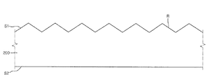
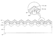
R テクスチュア構造
S1 半導体基板の第1面
S2 半導体基板の第2面
DP1 第1ドーピング物質層
DP2 第2ドーピング物質層
t 第1ドーピング物質層及び第2ドーピング物質層が形成するガラス層の厚み
Claims (14)
- 第1導電型を有する半導体基板に、前記第1導電型と異なる第2導電型を有する第1ドーピング物質層を形成する先蒸着段階と、
前記第1ドーピング物質層が形成された前記半導体基板を加熱する熱拡散段階と、
前記熱拡散段階後、前記第1ドーピング物質層上に、前記第2導電型を有する第2ドーピング物質層を形成する後蒸着段階と、
前記半導体基板、前記第1ドーピング物質層及び前記第2ドーピング物質層の一部をレーザで局所加熱し、前記半導体基板の第1面上にコンタクト層を形成する局所加熱段階と、
前記局所加熱段階後、前記第1ドーピング物質層及び第2ドーピング物質層を除去する段階と、
前記コンタクト層上に第1電極を形成し、前記半導体基板の前記第1面と対向する第2面上に第2電極を形成する段階と、
を含み、
前記後蒸着段階は、前記先蒸着段階よりも工程時間が短く、
前記先蒸着段階は、前記半導体基板が存在する蒸着チャンバ内に、POCl 3 を含む第1ドーピングソースを提供する段階を含み、前記後蒸着段階は、前記蒸着チャンバ内に、POCl 3 を含む第2ドーピングソースを提供する段階を含むことを特徴とする光電素子の製造方法。 - 前記第1ドーピングソースを提供する段階は、第1工程時間の間行われ、
前記第2ドーピングソースを提供する段階は、第2工程時間の間行われ、
前記第1工程時間は、前記第2工程時間より長いことを特徴とする請求項1に記載の光電素子の製造方法。 - 前記第1ドーピングソースを提供する段階では、前記第1ドーピングソースは、キャリアガスを介して供給され、前記第1ドーピングソースは第1濃度を有し、
前記第2ドーピングソースを提供する段階では、前記第2ドーピングソースは、キャリアガスを介して供給され、前記第2ドーピングソースは第2濃度を有し、
前記第2濃度は、前記第1濃度より高いことを特徴とする請求項1又は2に記載の光電素子の製造方法。 - 前記第1ドーピングソースを提供する段階では、
前記第1ドーピングソースは、キャリアガスを介して供給され、前記第1ドーピングソースは5体積%〜7体積%の濃度を有することを特徴とする請求項1〜3のいずれか一項に記載の光電素子の製造方法。 - 前記第1ドーピングソースを提供する段階は、10分〜20分間行われることを特徴とする請求項1〜4のいずれか一項に記載の光電素子の製造方法。
- 前記第2ドーピングソースを提供する段階では、
前記第2ドーピングソースは、キャリアガスを介して供給され、前記第2ドーピングソースは10体積%以上の濃度を有することを特徴とする請求項1〜5のいずれか一項に記載の光電素子の製造方法。 - 前記第2ドーピングソースを提供する段階は、3分〜8分間行われることを特徴とする請求項1〜6のいずれか一項に記載の光電素子の製造方法。
- 前記熱拡散段階は、不活性雰囲気下で、800℃〜900℃で30分〜50分間行われることを特徴とする請求項1〜7のいずれか一項に記載の光電素子の製造方法。
- 前記熱拡散段階では、前記半導体基板の前記第1面にエミッタ層を形成することを特徴とする請求項1〜8のいずれか一項に記載の光電素子の製造方法。
- 前記局所加熱段階では、
前記半導体基板の前記第1面に、前記コンタクト層より低いドーピング濃度を有し、前記コンタクト層と接するウィンドウ層を形成することを特徴とする請求項1〜9のいずれか一項に記載の光電素子の製造方法。 - 前記第1ドーピング物質層及び第2ドーピング物質層を除去する段階では、酸性溶液のエッチャントを利用してエッチングすることを特徴とする請求項1に記載の光電素子の製造方法。
- 前記局所加熱段階後、前記半導体基板上に反射防止膜を形成する段階をさらに含むことを特徴とする請求項1〜11のいずれか一項に記載の光電素子の製造方法。
- 前記半導体基板の前記第2面上に、前記第1導電型を有する背面電界層を形成する段階をさらに含むことを特徴とする請求項1〜12のいずれか一項に記載の光電素子の製造方法。
- 第1導電型の半導体基板に前記第1導電型と異なる第2導電型を有する第1ドーピング物質層を形成する先蒸着段階と、
前記第1ドーピング物質層のドーパントを前記半導体基板に拡散させ、前記半導体基板の第1面にエミッタ層を形成する拡散段階と、
前記拡散段階後、前記第2導電型を有する第2ドーピング物質層を形成する後蒸着段階と、
前記第1ドーピング物質層及び前記第2ドーピング物質層のドーパントを前記エミッタ層に拡散させ、前記半導体基板の前記第1面の一部にコンタクト層を形成する選択的拡散段階と、
前記選択的拡散段階後、前記第1ドーピング物質層及び第2ドーピング物質層を除去する段階と、
を含み、
前記後蒸着段階後、前記第1ドーピング物質層と前記第2ドーピング物質層は、変化する濃度勾配を有し、前記第1ドーピング物質層及び前記第2ドーピング物質層のシリコン酸化物の濃度は、前記半導体基板に近づくほど上昇し、
前記後蒸着段階は、前記先蒸着段階よりも工程時間が短く、
前記先蒸着段階は、前記半導体基板が存在する蒸着チャンバ内に、POCl 3 を含む第1ドーピングソースを提供する段階を含み、前記後蒸着段階は、前記蒸着チャンバ内に、POCl 3 を含む第2ドーピングソースを提供する段階を含むことを特徴とする光電素子の製造方法。
Applications Claiming Priority (4)
| Application Number | Priority Date | Filing Date | Title |
|---|---|---|---|
| US201161546642P | 2011-10-13 | 2011-10-13 | |
| US61/546642 | 2011-10-13 | ||
| US13/568462 | 2012-08-07 | ||
| US13/568,462 US8664015B2 (en) | 2011-10-13 | 2012-08-07 | Method of manufacturing photoelectric device |
Publications (2)
| Publication Number | Publication Date |
|---|---|
| JP2013089955A JP2013089955A (ja) | 2013-05-13 |
| JP6258576B2 true JP6258576B2 (ja) | 2018-01-10 |
Family
ID=46963476
Family Applications (1)
| Application Number | Title | Priority Date | Filing Date |
|---|---|---|---|
| JP2012219627A Active JP6258576B2 (ja) | 2011-10-13 | 2012-10-01 | 光電素子の製造方法 |
Country Status (5)
| Country | Link |
|---|---|
| US (1) | US8664015B2 (ja) |
| EP (1) | EP2581950A3 (ja) |
| JP (1) | JP6258576B2 (ja) |
| KR (1) | KR20130040125A (ja) |
| CN (1) | CN103050568A (ja) |
Families Citing this family (18)
| Publication number | Priority date | Publication date | Assignee | Title |
|---|---|---|---|---|
| DE102010054370A1 (de) * | 2010-12-13 | 2012-06-14 | Centrotherm Photovoltaics Ag | Verfahren zur Herstellung von Siliziumsolarzellen mit vorderseitiger Textur und glatter Rückseitenoberfläche |
| EP2654090B1 (en) * | 2012-04-17 | 2020-07-08 | LG Electronics, Inc. | Solar cell |
| KR101387718B1 (ko) | 2012-05-07 | 2014-04-22 | 엘지전자 주식회사 | 태양 전지 및 이의 제조 방법 |
| US8722545B2 (en) * | 2012-08-27 | 2014-05-13 | Stmicroelectronics Pte Ltd. | Method of selectively deglazing P205 |
| TW201432925A (zh) * | 2013-02-08 | 2014-08-16 | Ind Tech Res Inst | 矽晶太陽能電池結構 |
| CN104143583B (zh) * | 2013-05-08 | 2016-08-03 | 昱晶能源科技股份有限公司 | 制造太阳能电池的方法及太阳能电池 |
| KR20150048430A (ko) * | 2013-10-28 | 2015-05-07 | 현대중공업 주식회사 | 태양전지의 전극 패터닝 방법 및 이에 의한 태양전지 |
| JP6144778B2 (ja) * | 2013-12-13 | 2017-06-07 | 信越化学工業株式会社 | 太陽電池の製造方法 |
| JP6291341B2 (ja) * | 2014-05-12 | 2018-03-14 | キヤノン株式会社 | 基台をクリーニングする方法、半導体ウエハの熱処理方法、及び固体撮像装置の製造方法 |
| CN105322056A (zh) * | 2015-12-07 | 2016-02-10 | 中国科学院半导体研究所 | 一种选择性结构太阳电池的制备方法 |
| US20190067477A1 (en) * | 2017-08-28 | 2019-02-28 | United Microelectronics Corp. | Semiconductor structure with doped fin-shaped structures and method of fabricating the same |
| CN107993930A (zh) * | 2017-12-05 | 2018-05-04 | 苏州润阳光伏科技有限公司 | 磷扩散均匀性的修复方法 |
| CN110335814B (zh) * | 2019-07-05 | 2021-10-22 | 晶澳(扬州)太阳能科技有限公司 | 在硅片上制备选择性掺杂结构的制备方法及太阳能电池片 |
| CN111524797A (zh) * | 2020-04-26 | 2020-08-11 | 泰州中来光电科技有限公司 | 一种选择性发射极的制备方法 |
| CN111739794B (zh) * | 2020-06-30 | 2024-01-30 | 浙江晶科能源有限公司 | 硼扩散方法、太阳能电池及其制作方法 |
| CN114188436B (zh) * | 2020-09-15 | 2024-03-15 | 一道新能源科技股份有限公司 | 一种硅基底制备方法及太阳能电池 |
| CN113594299B (zh) * | 2021-07-27 | 2024-01-26 | 普乐新能源科技(泰兴)有限公司 | 一种n型硅片p++结构的制作工艺 |
| CN114709277B (zh) * | 2022-05-31 | 2022-09-23 | 浙江晶科能源有限公司 | 太阳能电池及其制备方法、光伏组件 |
Family Cites Families (26)
| Publication number | Priority date | Publication date | Assignee | Title |
|---|---|---|---|---|
| JPS4926456B1 (ja) * | 1970-03-02 | 1974-07-09 | ||
| JPS56130916A (en) * | 1980-03-17 | 1981-10-14 | Matsushita Electric Ind Co Ltd | Manufacture of semiconductor device |
| JP2004281569A (ja) * | 2003-03-13 | 2004-10-07 | Kyocera Corp | 太陽電池素子の製造方法 |
| US6998288B1 (en) * | 2003-10-03 | 2006-02-14 | Sunpower Corporation | Use of doped silicon dioxide in the fabrication of solar cells |
| DE102004036220B4 (de) * | 2004-07-26 | 2009-04-02 | Jürgen H. Werner | Verfahren zur Laserdotierung von Festkörpern mit einem linienfokussierten Laserstrahl |
| WO2007085452A1 (de) * | 2006-01-25 | 2007-08-02 | Fraunhofer-Gesellschaft zur Förderung der angewandten Forschung e.V. | Verfahren und vorrichtung zur präzisionsbearbeitung von substraten mittels eines in einen flüssigkeitsstrahl eingekoppelten laser und dessen verwendung |
| US8222516B2 (en) * | 2008-02-20 | 2012-07-17 | Sunpower Corporation | Front contact solar cell with formed emitter |
| JP4610630B2 (ja) | 2008-03-31 | 2011-01-12 | 三菱電機株式会社 | 太陽電池用拡散層の製造方法および太陽電池セルの製造方法 |
| KR100965600B1 (ko) | 2008-04-08 | 2010-06-23 | 주식회사 효성 | 실리콘 태양전지와 그의 제조방법 및 제조장치 |
| JP4712073B2 (ja) | 2008-07-11 | 2011-06-29 | 三菱電機株式会社 | 太陽電池用拡散層の製造方法および太陽電池セルの製造方法 |
| US8293568B2 (en) | 2008-07-28 | 2012-10-23 | Day4 Energy Inc. | Crystalline silicon PV cell with selective emitter produced with low temperature precision etch back and passivation process |
| US7897434B2 (en) * | 2008-08-12 | 2011-03-01 | International Business Machines Corporation | Methods of fabricating solar cell chips |
| TWI389322B (zh) | 2008-09-16 | 2013-03-11 | Gintech Energy Corp | 具有差異性摻雜之太陽能電池的製造方法 |
| KR20100032161A (ko) | 2008-09-17 | 2010-03-25 | 주식회사 효성 | 태양전지 제조방법 및 장치 |
| US8088675B2 (en) * | 2008-09-19 | 2012-01-03 | Applied Materials, Inc. | Methods of making an emitter having a desired dopant profile |
| US8053343B2 (en) | 2009-02-05 | 2011-11-08 | Snt. Co., Ltd. | Method for forming selective emitter of solar cell and diffusion apparatus for forming the same |
| KR101145928B1 (ko) | 2009-03-11 | 2012-05-15 | 엘지전자 주식회사 | 태양 전지 및 태양 전지의 제조 방법 |
| KR101155563B1 (ko) | 2009-05-27 | 2012-06-19 | 주식회사 효성 | 레이저를 이용한 태양전지 제조방법 |
| KR101161810B1 (ko) | 2009-08-21 | 2012-07-03 | 주식회사 효성 | 태양전지의 선택적 에미터 형성방법 및 그 태양전지 제조방법 |
| KR101083372B1 (ko) | 2009-10-14 | 2011-11-14 | 주식회사 효성 | 보론 도핑방법 및 이를 이용한 태양전지 제조방법 |
| US8614115B2 (en) * | 2009-10-30 | 2013-12-24 | International Business Machines Corporation | Photovoltaic solar cell device manufacture |
| US20110126877A1 (en) * | 2009-11-27 | 2011-06-02 | Jinah Kim | Solar cell |
| EP2395554A3 (en) * | 2010-06-14 | 2015-03-11 | Imec | Fabrication method for interdigitated back contact photovoltaic cells |
| CN103262266A (zh) * | 2010-08-02 | 2013-08-21 | 森特瑟姆光伏股份有限公司 | 包括选择性发射极的太阳能电池的制造方法 |
| TWI497737B (zh) * | 2010-12-02 | 2015-08-21 | Au Optronics Corp | 太陽能電池及其製造方法 |
| EP2490268A1 (en) * | 2011-02-03 | 2012-08-22 | Imec | Method for fabricating photovoltaic cells |
-
2012
- 2012-08-07 US US13/568,462 patent/US8664015B2/en active Active
- 2012-08-31 KR KR1020120096704A patent/KR20130040125A/ko not_active Application Discontinuation
- 2012-09-13 EP EP12184308.0A patent/EP2581950A3/en not_active Withdrawn
- 2012-09-28 CN CN2012103711538A patent/CN103050568A/zh active Pending
- 2012-10-01 JP JP2012219627A patent/JP6258576B2/ja active Active
Also Published As
| Publication number | Publication date |
|---|---|
| EP2581950A3 (en) | 2014-11-26 |
| KR20130040125A (ko) | 2013-04-23 |
| US20130095597A1 (en) | 2013-04-18 |
| EP2581950A2 (en) | 2013-04-17 |
| JP2013089955A (ja) | 2013-05-13 |
| US8664015B2 (en) | 2014-03-04 |
| CN103050568A (zh) | 2013-04-17 |
Similar Documents
| Publication | Publication Date | Title |
|---|---|---|
| JP6258576B2 (ja) | 光電素子の製造方法 | |
| JP5490231B2 (ja) | 太陽電池素子およびその製造方法ならびに太陽電池モジュール | |
| JP6285545B2 (ja) | 太陽電池素子および太陽電池モジュール | |
| JP2006516830A (ja) | 改良された光起電電池及びその製造 | |
| JP5991945B2 (ja) | 太陽電池および太陽電池モジュール | |
| CN108039374A (zh) | n型双面太阳电池的制备方法 | |
| JP5338702B2 (ja) | 太陽電池の製造方法 | |
| JP2014011246A (ja) | 太陽電池素子および太陽電池モジュール | |
| TWI695518B (zh) | 高光電變換效率太陽電池及高光電變換效率太陽電池之製造方法 | |
| WO2013100085A1 (ja) | 太陽電池素子、太陽電池素子の製造方法および太陽電池モジュール | |
| JP6426486B2 (ja) | 太陽電池素子の製造方法 | |
| JP5623131B2 (ja) | 太陽電池素子およびその製造方法ならびに太陽電池モジュール | |
| JP6330108B1 (ja) | 高光電変換効率太陽電池及び高光電変換効率太陽電池の製造方法 | |
| JP6220483B1 (ja) | 高光電変換効率太陽電池及び高光電変換効率太陽電池の製造方法 | |
| JP5744202B2 (ja) | アルミナ膜の形成方法 | |
| CN115692516A (zh) | 一种新型topcon电池及其制作方法 | |
| KR101198430B1 (ko) | 양면 수광형 국부화 에미터 태양전지 및 그 제조 방법 | |
| JP6430842B2 (ja) | 太陽電池素子の製造方法および太陽電池モジュールの製造方法 | |
| JP6114205B2 (ja) | 太陽電池の製造方法 | |
| KR101181625B1 (ko) | 국부화 에미터 태양전지 및 그 제조 방법 | |
| KR101382047B1 (ko) | 태양전지의 선택적 에미터 형성방법 | |
| JP6741626B2 (ja) | 高効率裏面電極型太陽電池及びその製造方法 | |
| TWI482294B (zh) | 製作背面具有介電質層以及分散式接觸電極之矽太陽能電池之方法及該元件 | |
| TWI447927B (zh) | 以抗蝕材料製作局部正面蝕刻之太陽能電池之方法 | |
| KR20120026683A (ko) | 태양전지의 제조방법 |
Legal Events
| Date | Code | Title | Description |
|---|---|---|---|
| A711 | Notification of change in applicant |
Free format text: JAPANESE INTERMEDIATE CODE: A711 Effective date: 20150723 |
|
| A621 | Written request for application examination |
Free format text: JAPANESE INTERMEDIATE CODE: A621 Effective date: 20150930 |
|
| A977 | Report on retrieval |
Free format text: JAPANESE INTERMEDIATE CODE: A971007 Effective date: 20160720 |
|
| A131 | Notification of reasons for refusal |
Free format text: JAPANESE INTERMEDIATE CODE: A131 Effective date: 20160726 |
|
| A601 | Written request for extension of time |
Free format text: JAPANESE INTERMEDIATE CODE: A601 Effective date: 20161026 |
|
| A521 | Request for written amendment filed |
Free format text: JAPANESE INTERMEDIATE CODE: A523 Effective date: 20161202 |
|
| A131 | Notification of reasons for refusal |
Free format text: JAPANESE INTERMEDIATE CODE: A131 Effective date: 20170314 |
|
| A521 | Request for written amendment filed |
Free format text: JAPANESE INTERMEDIATE CODE: A523 Effective date: 20170609 |
|
| TRDD | Decision of grant or rejection written | ||
| A01 | Written decision to grant a patent or to grant a registration (utility model) |
Free format text: JAPANESE INTERMEDIATE CODE: A01 Effective date: 20171128 |
|
| A61 | First payment of annual fees (during grant procedure) |
Free format text: JAPANESE INTERMEDIATE CODE: A61 Effective date: 20171207 |
|
| R150 | Certificate of patent or registration of utility model |
Ref document number: 6258576 Country of ref document: JP Free format text: JAPANESE INTERMEDIATE CODE: R150 |
|
| R250 | Receipt of annual fees |
Free format text: JAPANESE INTERMEDIATE CODE: R250 |
|
| R250 | Receipt of annual fees |
Free format text: JAPANESE INTERMEDIATE CODE: R250 |
|
| R250 | Receipt of annual fees |
Free format text: JAPANESE INTERMEDIATE CODE: R250 |
|
| R250 | Receipt of annual fees |
Free format text: JAPANESE INTERMEDIATE CODE: R250 |