JP6258576B2 - Method for manufacturing photoelectric device - Google Patents
Method for manufacturing photoelectric device Download PDFInfo
- Publication number
- JP6258576B2 JP6258576B2 JP2012219627A JP2012219627A JP6258576B2 JP 6258576 B2 JP6258576 B2 JP 6258576B2 JP 2012219627 A JP2012219627 A JP 2012219627A JP 2012219627 A JP2012219627 A JP 2012219627A JP 6258576 B2 JP6258576 B2 JP 6258576B2
- Authority
- JP
- Japan
- Prior art keywords
- doping
- semiconductor substrate
- material layer
- layer
- doping material
- Prior art date
- Legal status (The legal status is an assumption and is not a legal conclusion. Google has not performed a legal analysis and makes no representation as to the accuracy of the status listed.)
- Active
Links
- 238000000034 method Methods 0.000 title claims description 71
- 238000004519 manufacturing process Methods 0.000 title claims description 40
- 239000000758 substrate Substances 0.000 claims description 120
- 239000004065 semiconductor Substances 0.000 claims description 119
- 239000000463 material Substances 0.000 claims description 96
- 238000009792 diffusion process Methods 0.000 claims description 63
- 239000002019 doping agent Substances 0.000 claims description 38
- RLOWWWKZYUNIDI-UHFFFAOYSA-N phosphinic chloride Chemical compound ClP=O RLOWWWKZYUNIDI-UHFFFAOYSA-N 0.000 claims description 28
- 230000008021 deposition Effects 0.000 claims description 27
- 238000010438 heat treatment Methods 0.000 claims description 22
- 238000005530 etching Methods 0.000 claims description 13
- 239000012159 carrier gas Substances 0.000 claims description 12
- VYPSYNLAJGMNEJ-UHFFFAOYSA-N Silicium dioxide Chemical compound O=[Si]=O VYPSYNLAJGMNEJ-UHFFFAOYSA-N 0.000 claims description 8
- 229910052814 silicon oxide Inorganic materials 0.000 claims description 8
- 239000003929 acidic solution Substances 0.000 claims description 3
- 238000013459 approach Methods 0.000 claims description 2
- 239000010410 layer Substances 0.000 description 186
- 238000005137 deposition process Methods 0.000 description 60
- 230000000052 comparative effect Effects 0.000 description 25
- 238000000151 deposition Methods 0.000 description 23
- 238000005215 recombination Methods 0.000 description 15
- 230000006798 recombination Effects 0.000 description 15
- 239000000969 carrier Substances 0.000 description 12
- 239000011521 glass Substances 0.000 description 10
- PXHVJJICTQNCMI-UHFFFAOYSA-N Nickel Chemical compound [Ni] PXHVJJICTQNCMI-UHFFFAOYSA-N 0.000 description 9
- 239000005360 phosphosilicate glass Substances 0.000 description 9
- 229910004298 SiO 2 Inorganic materials 0.000 description 8
- 238000010248 power generation Methods 0.000 description 8
- IJGRMHOSHXDMSA-UHFFFAOYSA-N Atomic nitrogen Chemical compound N#N IJGRMHOSHXDMSA-UHFFFAOYSA-N 0.000 description 7
- OAICVXFJPJFONN-UHFFFAOYSA-N Phosphorus Chemical compound [P] OAICVXFJPJFONN-UHFFFAOYSA-N 0.000 description 6
- HEMHJVSKTPXQMS-UHFFFAOYSA-M Sodium hydroxide Chemical compound [OH-].[Na+] HEMHJVSKTPXQMS-UHFFFAOYSA-M 0.000 description 6
- 239000010949 copper Substances 0.000 description 6
- 239000002003 electrode paste Substances 0.000 description 6
- 229910052698 phosphorus Inorganic materials 0.000 description 6
- 239000011574 phosphorus Substances 0.000 description 6
- 239000007787 solid Substances 0.000 description 6
- 238000007740 vapor deposition Methods 0.000 description 6
- 238000005229 chemical vapour deposition Methods 0.000 description 5
- 230000005684 electric field Effects 0.000 description 5
- 238000001704 evaporation Methods 0.000 description 5
- 239000007789 gas Substances 0.000 description 5
- HQVNEWCFYHHQES-UHFFFAOYSA-N silicon nitride Chemical compound N12[Si]34N5[Si]62N3[Si]51N64 HQVNEWCFYHHQES-UHFFFAOYSA-N 0.000 description 5
- 229910052581 Si3N4 Inorganic materials 0.000 description 4
- QVGXLLKOCUKJST-UHFFFAOYSA-N atomic oxygen Chemical compound [O] QVGXLLKOCUKJST-UHFFFAOYSA-N 0.000 description 4
- 230000007423 decrease Effects 0.000 description 4
- 230000008020 evaporation Effects 0.000 description 4
- 239000007769 metal material Substances 0.000 description 4
- 239000001301 oxygen Substances 0.000 description 4
- 229910052760 oxygen Inorganic materials 0.000 description 4
- 238000002161 passivation Methods 0.000 description 4
- XHXFXVLFKHQFAL-UHFFFAOYSA-N phosphoryl trichloride Chemical compound ClP(Cl)(Cl)=O XHXFXVLFKHQFAL-UHFFFAOYSA-N 0.000 description 4
- 230000002265 prevention Effects 0.000 description 4
- 238000007650 screen-printing Methods 0.000 description 4
- 238000005019 vapor deposition process Methods 0.000 description 4
- QTBSBXVTEAMEQO-UHFFFAOYSA-N Acetic acid Chemical compound CC(O)=O QTBSBXVTEAMEQO-UHFFFAOYSA-N 0.000 description 3
- RYGMFSIKBFXOCR-UHFFFAOYSA-N Copper Chemical compound [Cu] RYGMFSIKBFXOCR-UHFFFAOYSA-N 0.000 description 3
- KRHYYFGTRYWZRS-UHFFFAOYSA-N Fluorane Chemical compound F KRHYYFGTRYWZRS-UHFFFAOYSA-N 0.000 description 3
- XUIMIQQOPSSXEZ-UHFFFAOYSA-N Silicon Chemical compound [Si] XUIMIQQOPSSXEZ-UHFFFAOYSA-N 0.000 description 3
- BQCADISMDOOEFD-UHFFFAOYSA-N Silver Chemical compound [Ag] BQCADISMDOOEFD-UHFFFAOYSA-N 0.000 description 3
- 229910052782 aluminium Inorganic materials 0.000 description 3
- XAGFODPZIPBFFR-UHFFFAOYSA-N aluminium Chemical compound [Al] XAGFODPZIPBFFR-UHFFFAOYSA-N 0.000 description 3
- 238000006243 chemical reaction Methods 0.000 description 3
- 229910052802 copper Inorganic materials 0.000 description 3
- 230000003247 decreasing effect Effects 0.000 description 3
- 229910052759 nickel Inorganic materials 0.000 description 3
- 229910052757 nitrogen Inorganic materials 0.000 description 3
- 238000004904 shortening Methods 0.000 description 3
- 229910052709 silver Inorganic materials 0.000 description 3
- 239000004332 silver Substances 0.000 description 3
- 239000002131 composite material Substances 0.000 description 2
- 238000010586 diagram Methods 0.000 description 2
- 238000001035 drying Methods 0.000 description 2
- 238000012986 modification Methods 0.000 description 2
- 230000004048 modification Effects 0.000 description 2
- 229910021421 monocrystalline silicon Inorganic materials 0.000 description 2
- 230000003647 oxidation Effects 0.000 description 2
- 238000007254 oxidation reaction Methods 0.000 description 2
- 229910052710 silicon Inorganic materials 0.000 description 2
- 239000010703 silicon Substances 0.000 description 2
- 239000002356 single layer Substances 0.000 description 2
- 239000000126 substance Substances 0.000 description 2
- XLYOFNOQVPJJNP-UHFFFAOYSA-N water Chemical compound O XLYOFNOQVPJJNP-UHFFFAOYSA-N 0.000 description 2
- GRYLNZFGIOXLOG-UHFFFAOYSA-N Nitric acid Chemical compound O[N+]([O-])=O GRYLNZFGIOXLOG-UHFFFAOYSA-N 0.000 description 1
- KWYUFKZDYYNOTN-UHFFFAOYSA-M Potassium hydroxide Chemical compound [OH-].[K+] KWYUFKZDYYNOTN-UHFFFAOYSA-M 0.000 description 1
- 239000002253 acid Substances 0.000 description 1
- 239000003513 alkali Substances 0.000 description 1
- 239000012670 alkaline solution Substances 0.000 description 1
- 239000002585 base Substances 0.000 description 1
- 238000004140 cleaning Methods 0.000 description 1
- 238000010344 co-firing Methods 0.000 description 1
- 229910021419 crystalline silicon Inorganic materials 0.000 description 1
- 230000002950 deficient Effects 0.000 description 1
- 239000008367 deionised water Substances 0.000 description 1
- 229910021641 deionized water Inorganic materials 0.000 description 1
- 230000001066 destructive effect Effects 0.000 description 1
- 229910001873 dinitrogen Inorganic materials 0.000 description 1
- 230000000694 effects Effects 0.000 description 1
- 230000005611 electricity Effects 0.000 description 1
- 230000007613 environmental effect Effects 0.000 description 1
- 238000010304 firing Methods 0.000 description 1
- 239000012535 impurity Substances 0.000 description 1
- 239000011261 inert gas Substances 0.000 description 1
- 230000001678 irradiating effect Effects 0.000 description 1
- 229910052751 metal Inorganic materials 0.000 description 1
- 239000002184 metal Substances 0.000 description 1
- 239000011259 mixed solution Substances 0.000 description 1
- 125000000896 monocarboxylic acid group Chemical group 0.000 description 1
- QPJSUIGXIBEQAC-UHFFFAOYSA-N n-(2,4-dichloro-5-propan-2-yloxyphenyl)acetamide Chemical compound CC(C)OC1=CC(NC(C)=O)=C(Cl)C=C1Cl QPJSUIGXIBEQAC-UHFFFAOYSA-N 0.000 description 1
- 229910017604 nitric acid Inorganic materials 0.000 description 1
- 150000004767 nitrides Chemical class 0.000 description 1
- 238000007747 plating Methods 0.000 description 1
- 229910021420 polycrystalline silicon Inorganic materials 0.000 description 1
- 239000002244 precipitate Substances 0.000 description 1
- 239000000243 solution Substances 0.000 description 1
Images


Classifications
-
- H—ELECTRICITY
- H01—ELECTRIC ELEMENTS
- H01L—SEMICONDUCTOR DEVICES NOT COVERED BY CLASS H10
- H01L31/00—Semiconductor devices sensitive to infrared radiation, light, electromagnetic radiation of shorter wavelength or corpuscular radiation and specially adapted either for the conversion of the energy of such radiation into electrical energy or for the control of electrical energy by such radiation; Processes or apparatus specially adapted for the manufacture or treatment thereof or of parts thereof; Details thereof
- H01L31/04—Semiconductor devices sensitive to infrared radiation, light, electromagnetic radiation of shorter wavelength or corpuscular radiation and specially adapted either for the conversion of the energy of such radiation into electrical energy or for the control of electrical energy by such radiation; Processes or apparatus specially adapted for the manufacture or treatment thereof or of parts thereof; Details thereof adapted as photovoltaic [PV] conversion devices
-
- H—ELECTRICITY
- H01—ELECTRIC ELEMENTS
- H01L—SEMICONDUCTOR DEVICES NOT COVERED BY CLASS H10
- H01L31/00—Semiconductor devices sensitive to infrared radiation, light, electromagnetic radiation of shorter wavelength or corpuscular radiation and specially adapted either for the conversion of the energy of such radiation into electrical energy or for the control of electrical energy by such radiation; Processes or apparatus specially adapted for the manufacture or treatment thereof or of parts thereof; Details thereof
- H01L31/18—Processes or apparatus specially adapted for the manufacture or treatment of these devices or of parts thereof
- H01L31/1804—Processes or apparatus specially adapted for the manufacture or treatment of these devices or of parts thereof comprising only elements of Group IV of the Periodic Table
-
- H—ELECTRICITY
- H01—ELECTRIC ELEMENTS
- H01L—SEMICONDUCTOR DEVICES NOT COVERED BY CLASS H10
- H01L21/00—Processes or apparatus adapted for the manufacture or treatment of semiconductor or solid state devices or of parts thereof
- H01L21/02—Manufacture or treatment of semiconductor devices or of parts thereof
- H01L21/04—Manufacture or treatment of semiconductor devices or of parts thereof the devices having potential barriers, e.g. a PN junction, depletion layer or carrier concentration layer
- H01L21/18—Manufacture or treatment of semiconductor devices or of parts thereof the devices having potential barriers, e.g. a PN junction, depletion layer or carrier concentration layer the devices having semiconductor bodies comprising elements of Group IV of the Periodic Table or AIIIBV compounds with or without impurities, e.g. doping materials
- H01L21/22—Diffusion of impurity materials, e.g. doping materials, electrode materials, into or out of a semiconductor body, or between semiconductor regions; Interactions between two or more impurities; Redistribution of impurities
- H01L21/223—Diffusion of impurity materials, e.g. doping materials, electrode materials, into or out of a semiconductor body, or between semiconductor regions; Interactions between two or more impurities; Redistribution of impurities using diffusion into or out of a solid from or into a gaseous phase
-
- H—ELECTRICITY
- H01—ELECTRIC ELEMENTS
- H01L—SEMICONDUCTOR DEVICES NOT COVERED BY CLASS H10
- H01L21/00—Processes or apparatus adapted for the manufacture or treatment of semiconductor or solid state devices or of parts thereof
- H01L21/02—Manufacture or treatment of semiconductor devices or of parts thereof
- H01L21/04—Manufacture or treatment of semiconductor devices or of parts thereof the devices having potential barriers, e.g. a PN junction, depletion layer or carrier concentration layer
- H01L21/18—Manufacture or treatment of semiconductor devices or of parts thereof the devices having potential barriers, e.g. a PN junction, depletion layer or carrier concentration layer the devices having semiconductor bodies comprising elements of Group IV of the Periodic Table or AIIIBV compounds with or without impurities, e.g. doping materials
- H01L21/22—Diffusion of impurity materials, e.g. doping materials, electrode materials, into or out of a semiconductor body, or between semiconductor regions; Interactions between two or more impurities; Redistribution of impurities
- H01L21/225—Diffusion of impurity materials, e.g. doping materials, electrode materials, into or out of a semiconductor body, or between semiconductor regions; Interactions between two or more impurities; Redistribution of impurities using diffusion into or out of a solid from or into a solid phase, e.g. a doped oxide layer
- H01L21/2251—Diffusion into or out of group IV semiconductors
- H01L21/2254—Diffusion into or out of group IV semiconductors from or through or into an applied layer, e.g. photoresist, nitrides
- H01L21/2255—Diffusion into or out of group IV semiconductors from or through or into an applied layer, e.g. photoresist, nitrides the applied layer comprising oxides only, e.g. P2O5, PSG, H3BO3, doped oxides
- H01L21/2256—Diffusion into or out of group IV semiconductors from or through or into an applied layer, e.g. photoresist, nitrides the applied layer comprising oxides only, e.g. P2O5, PSG, H3BO3, doped oxides through the applied layer
-
- H—ELECTRICITY
- H01—ELECTRIC ELEMENTS
- H01L—SEMICONDUCTOR DEVICES NOT COVERED BY CLASS H10
- H01L21/00—Processes or apparatus adapted for the manufacture or treatment of semiconductor or solid state devices or of parts thereof
- H01L21/02—Manufacture or treatment of semiconductor devices or of parts thereof
- H01L21/04—Manufacture or treatment of semiconductor devices or of parts thereof the devices having potential barriers, e.g. a PN junction, depletion layer or carrier concentration layer
- H01L21/18—Manufacture or treatment of semiconductor devices or of parts thereof the devices having potential barriers, e.g. a PN junction, depletion layer or carrier concentration layer the devices having semiconductor bodies comprising elements of Group IV of the Periodic Table or AIIIBV compounds with or without impurities, e.g. doping materials
- H01L21/26—Bombardment with radiation
- H01L21/263—Bombardment with radiation with high-energy radiation
- H01L21/268—Bombardment with radiation with high-energy radiation using electromagnetic radiation, e.g. laser radiation
-
- H—ELECTRICITY
- H01—ELECTRIC ELEMENTS
- H01L—SEMICONDUCTOR DEVICES NOT COVERED BY CLASS H10
- H01L31/00—Semiconductor devices sensitive to infrared radiation, light, electromagnetic radiation of shorter wavelength or corpuscular radiation and specially adapted either for the conversion of the energy of such radiation into electrical energy or for the control of electrical energy by such radiation; Processes or apparatus specially adapted for the manufacture or treatment thereof or of parts thereof; Details thereof
- H01L31/02—Details
- H01L31/0216—Coatings
-
- H—ELECTRICITY
- H01—ELECTRIC ELEMENTS
- H01L—SEMICONDUCTOR DEVICES NOT COVERED BY CLASS H10
- H01L31/00—Semiconductor devices sensitive to infrared radiation, light, electromagnetic radiation of shorter wavelength or corpuscular radiation and specially adapted either for the conversion of the energy of such radiation into electrical energy or for the control of electrical energy by such radiation; Processes or apparatus specially adapted for the manufacture or treatment thereof or of parts thereof; Details thereof
- H01L31/02—Details
- H01L31/0236—Special surface textures
- H01L31/02363—Special surface textures of the semiconductor body itself, e.g. textured active layers
-
- H—ELECTRICITY
- H01—ELECTRIC ELEMENTS
- H01L—SEMICONDUCTOR DEVICES NOT COVERED BY CLASS H10
- H01L31/00—Semiconductor devices sensitive to infrared radiation, light, electromagnetic radiation of shorter wavelength or corpuscular radiation and specially adapted either for the conversion of the energy of such radiation into electrical energy or for the control of electrical energy by such radiation; Processes or apparatus specially adapted for the manufacture or treatment thereof or of parts thereof; Details thereof
- H01L31/04—Semiconductor devices sensitive to infrared radiation, light, electromagnetic radiation of shorter wavelength or corpuscular radiation and specially adapted either for the conversion of the energy of such radiation into electrical energy or for the control of electrical energy by such radiation; Processes or apparatus specially adapted for the manufacture or treatment thereof or of parts thereof; Details thereof adapted as photovoltaic [PV] conversion devices
- H01L31/06—Semiconductor devices sensitive to infrared radiation, light, electromagnetic radiation of shorter wavelength or corpuscular radiation and specially adapted either for the conversion of the energy of such radiation into electrical energy or for the control of electrical energy by such radiation; Processes or apparatus specially adapted for the manufacture or treatment thereof or of parts thereof; Details thereof adapted as photovoltaic [PV] conversion devices characterised by potential barriers
- H01L31/068—Semiconductor devices sensitive to infrared radiation, light, electromagnetic radiation of shorter wavelength or corpuscular radiation and specially adapted either for the conversion of the energy of such radiation into electrical energy or for the control of electrical energy by such radiation; Processes or apparatus specially adapted for the manufacture or treatment thereof or of parts thereof; Details thereof adapted as photovoltaic [PV] conversion devices characterised by potential barriers the potential barriers being only of the PN homojunction type, e.g. bulk silicon PN homojunction solar cells or thin film polycrystalline silicon PN homojunction solar cells
-
- H—ELECTRICITY
- H01—ELECTRIC ELEMENTS
- H01L—SEMICONDUCTOR DEVICES NOT COVERED BY CLASS H10
- H01L31/00—Semiconductor devices sensitive to infrared radiation, light, electromagnetic radiation of shorter wavelength or corpuscular radiation and specially adapted either for the conversion of the energy of such radiation into electrical energy or for the control of electrical energy by such radiation; Processes or apparatus specially adapted for the manufacture or treatment thereof or of parts thereof; Details thereof
- H01L31/18—Processes or apparatus specially adapted for the manufacture or treatment of these devices or of parts thereof
-
- Y—GENERAL TAGGING OF NEW TECHNOLOGICAL DEVELOPMENTS; GENERAL TAGGING OF CROSS-SECTIONAL TECHNOLOGIES SPANNING OVER SEVERAL SECTIONS OF THE IPC; TECHNICAL SUBJECTS COVERED BY FORMER USPC CROSS-REFERENCE ART COLLECTIONS [XRACs] AND DIGESTS
- Y02—TECHNOLOGIES OR APPLICATIONS FOR MITIGATION OR ADAPTATION AGAINST CLIMATE CHANGE
- Y02E—REDUCTION OF GREENHOUSE GAS [GHG] EMISSIONS, RELATED TO ENERGY GENERATION, TRANSMISSION OR DISTRIBUTION
- Y02E10/00—Energy generation through renewable energy sources
- Y02E10/50—Photovoltaic [PV] energy
- Y02E10/547—Monocrystalline silicon PV cells
-
- Y—GENERAL TAGGING OF NEW TECHNOLOGICAL DEVELOPMENTS; GENERAL TAGGING OF CROSS-SECTIONAL TECHNOLOGIES SPANNING OVER SEVERAL SECTIONS OF THE IPC; TECHNICAL SUBJECTS COVERED BY FORMER USPC CROSS-REFERENCE ART COLLECTIONS [XRACs] AND DIGESTS
- Y02—TECHNOLOGIES OR APPLICATIONS FOR MITIGATION OR ADAPTATION AGAINST CLIMATE CHANGE
- Y02P—CLIMATE CHANGE MITIGATION TECHNOLOGIES IN THE PRODUCTION OR PROCESSING OF GOODS
- Y02P70/00—Climate change mitigation technologies in the production process for final industrial or consumer products
- Y02P70/50—Manufacturing or production processes characterised by the final manufactured product
Landscapes
- Engineering & Computer Science (AREA)
- Physics & Mathematics (AREA)
- Power Engineering (AREA)
- Condensed Matter Physics & Semiconductors (AREA)
- General Physics & Mathematics (AREA)
- Computer Hardware Design (AREA)
- Microelectronics & Electronic Packaging (AREA)
- Manufacturing & Machinery (AREA)
- Electromagnetism (AREA)
- High Energy & Nuclear Physics (AREA)
- Optics & Photonics (AREA)
- Health & Medical Sciences (AREA)
- Toxicology (AREA)
- Life Sciences & Earth Sciences (AREA)
- Chemical & Material Sciences (AREA)
- Crystallography & Structural Chemistry (AREA)
- Sustainable Development (AREA)
- Photovoltaic Devices (AREA)
- Electrodes Of Semiconductors (AREA)
Description
本発明は、光電素子の製造方法に関する。 The present invention relates to a method for manufacturing a photoelectric element.
近年、エネルギー資源の枯渇問題や地球環境問題などによって、クリーンエネルギーの開発が加速化されている。太陽電池を利用した太陽光発電は、太陽光を直接電気に変換するためクリーンエネルギーであり、新たなエネルギーの源泉として期待されている。 In recent years, the development of clean energy has been accelerated due to the problem of depletion of energy resources and global environmental problems. Solar power generation using solar cells is clean energy because it converts sunlight directly into electricity, and is expected as a new source of energy.
しかし、現在工業的に生産されている太陽電池は、火力発電と比較してまだ発電コストが高い。太陽電池の広範囲な分野への応用のためには、太陽電池の発電効率をさらに高めることが必要であるが、従来の太陽電池は、発電効率が低いという問題があった。 However, industrially produced solar cells still have high power generation costs compared to thermal power generation. In order to apply solar cells to a wide range of fields, it is necessary to further increase the power generation efficiency of solar cells. However, conventional solar cells have a problem of low power generation efficiency.
そこで、本発明は、上記問題に鑑みてなされたものであり、本発明の目的とするところは、太陽電池の発電効率を高めることが可能な、新規かつ改良された光電素子の製造方法を提供することにある。 Accordingly, the present invention has been made in view of the above problems, and an object of the present invention is to provide a novel and improved photoelectric element manufacturing method capable of increasing the power generation efficiency of a solar cell. There is to do.
上記課題を解決するために、本発明のある観点によれば第1導電型を有する半導体基板に、前記第1導電型と異なる第2導電型を有する第1ドーピング物質層を形成する先蒸着段階と、前記第1ドーピング物質層が形成された前記半導体基板を加熱する熱拡散段階と、前記熱拡散段階後、前記第1ドーピング物質層上に、前記第2導電型を有する第2ドーピング物質層を形成する後蒸着段階と、前記半導体基板、前記第1ドーピング物質層及び前記第2ドーピング物質層の一部をレーザで局所加熱し、前記半導体基板の第1面上にコンタクト層を形成する局所加熱段階と、前記コンタクト層上に第1電極を形成し、前記半導体基板の前記第1面と対向する第2面上に第2電極を形成する段階と、を含む光電素の製造方法が提供される。 In order to solve the above problems, according to an aspect of the present invention, a pre-deposition step of forming a first doping material layer having a second conductivity type different from the first conductivity type on a semiconductor substrate having a first conductivity type. And a thermal diffusion step of heating the semiconductor substrate on which the first doping material layer is formed, and a second doping material layer having the second conductivity type on the first doping material layer after the thermal diffusion step. Forming a contact layer on the first surface of the semiconductor substrate by locally heating the semiconductor substrate, the first doping material layer, and a part of the second doping material layer with a laser; A method for producing a photoelectric element is provided, comprising: a heating step; and forming a first electrode on the contact layer and forming a second electrode on a second surface opposite to the first surface of the semiconductor substrate. Is done.
前記先蒸着段階は、半導体基板が存在する蒸着チャンバ内に、第1ドーピングソースを提供する段階を含み、前記後蒸着段階は、前記蒸着チャンバ内に、第2ドーピングソースを提供する段階を含んでもよい。 The pre-deposition step may include providing a first doping source in a deposition chamber in which a semiconductor substrate is present, and the post-deposition step may include providing a second doping source in the deposition chamber. Good.
前記第1ドーピングソースを提供する段階は、第1工程時間の間行われ、前記第2ドーピングソースを提供する段階は、第2工程時間の間行われ、前記第1工程時間は、前記第2工程時間より長くてもよい。 Providing the first doping source is performed for a first process time, providing the second doping source is performed for a second process time, and the first process time is the second process time. It may be longer than the process time.
前記第1ドーピングソースを提供する段階では、前記第1ドーピングソースは、キャリアガスを介して供給され、前記第1ドーピングソースは第1濃度を有し、前記第2ドーピングソースを提供する段階では、前記第2ドーピングソースは、キャリアガスを介して供給され、前記第2ドーピングソースが第2濃度を有し、前記第2濃度は、第1濃度より高くてもよい。 In providing the first doping source, the first doping source is supplied through a carrier gas, the first doping source has a first concentration, and in providing the second doping source, The second doping source may be supplied via a carrier gas, the second doping source may have a second concentration, and the second concentration may be higher than the first concentration.
前記第1ドーピングソースは、POCl3を含んでもよい。 The first doping source may include POCl 3 .
前記第1ドーピングソースを提供する段階では、前記第1ドーピングソースは、キャリアガスを介して供給され、前記第1ドーピングソースが5体積%〜7体積%の濃度を有してもよい。 In providing the first doping source, the first doping source may be supplied through a carrier gas, and the first doping source may have a concentration of 5% to 7% by volume.
前記第1ドーピングソースを提供する段階は、10分〜20分間行われてもよい。 The providing of the first doping source may be performed for 10 to 20 minutes.
前記第2ドーピングソースは、POCl3を含んでもよい。 The second doping source may include POCl 3 .
前記第2ドーピングソースを提供する段階では、前記第2ドーピングソースは、キャリアガスを介して供給され、前記第2ドーピングソースは10体積%以上の濃度を有してもよい。 In providing the second doping source, the second doping source may be supplied through a carrier gas, and the second doping source may have a concentration of 10% by volume or more.
前記第2ドーピングソースを提供する段階は、3分〜8分間行われてもよい。 The providing of the second doping source may be performed for 3 to 8 minutes.
前記熱拡散段階は、不活性雰囲気下で、800℃〜900℃で30分〜50分間行われてもよい。 The thermal diffusion step may be performed at 800 ° C. to 900 ° C. for 30 minutes to 50 minutes under an inert atmosphere.
前記熱拡散段階では、前記半導体基板の前記第1面にエミッタ層を形成してもよい。 In the thermal diffusion step, an emitter layer may be formed on the first surface of the semiconductor substrate.
前記局所加熱段階では、前記半導体基板の前記第1面に、前記コンタクト層より低いドーピング濃度を有し、前記コンタクト層と接するウィンドウ層を形成してもよい。 In the local heating step, a window layer having a lower doping concentration than the contact layer and in contact with the contact layer may be formed on the first surface of the semiconductor substrate.
前記光電素子の製造方法は、前記局所加熱段階後、前記第1ドーピング物質層及び第2ドーピング物質層を除去する段階をさらに含んでもよい。 The method for manufacturing the photoelectric device may further include a step of removing the first doping material layer and the second doping material layer after the local heating step.
前記第1ドーピング物質層及び第2ドーピング物質層を除去する段階では、酸性溶液のエッチャントを利用してエッチングしてもよい。 In the step of removing the first doping material layer and the second doping material layer, etching may be performed using an etchant of an acidic solution.
前記光電素子の製造方法は、前記局所加熱段階後、前記半導体基板上に反射防止膜を形成する段階をさらに含んでもよい。 The method for manufacturing the photoelectric device may further include a step of forming an antireflection film on the semiconductor substrate after the local heating step.
前記光電素子の製造方法は、前記半導体基板の前記第2面上に、前記第1導電型を有する背面電界層を形成する段階をさらに含んでもよい。 The method for manufacturing a photoelectric device may further include forming a back surface field layer having the first conductivity type on the second surface of the semiconductor substrate.
また、上記課題を解決するために、本発明の別の観点によれば、第1導電型の半導体基板に、前記第1導電型と異なる第2導電型を有する第1ドーピング物質層を形成する先蒸着段階と、前記第1ドーピング物質層のドーパントを前記半導体基板に拡散させ、前記半導体基板の第1面にエミッタ層を形成する拡散段階と、前記拡散段階後、前記第2導電型を有する第2ドーピング物質層を形成する後蒸着段階を含み、前記第1ドーピング物質層と前記第2ドーピング物質層は、変化する濃度勾配を有し、前記第1ドーピング物質層及び前記第2ドーピング物質層のシリコン酸化物の濃度は、前記半導体基板に近づくほど上昇し、前記第1ドーピング物質層及び前記第2ドーピング物質層のドーパントを前記エミッタ層に拡散させ、前記半導体基板の前記第1面の一部にコンタクト層を形成する選択的拡散段階と、を含む光電素子の製造方法が提供される。 In order to solve the above problem, according to another aspect of the present invention, a first doping material layer having a second conductivity type different from the first conductivity type is formed on a first conductivity type semiconductor substrate. A pre-deposition step, a diffusion step of diffusing the dopant of the first doping material layer into the semiconductor substrate and forming an emitter layer on the first surface of the semiconductor substrate; and after the diffusion step, having the second conductivity type A post-deposition step of forming a second doping material layer, wherein the first doping material layer and the second doping material layer have a varying concentration gradient, the first doping material layer and the second doping material layer; The concentration of the silicon oxide increases as it approaches the semiconductor substrate, and the dopant of the first doping material layer and the second doping material layer is diffused into the emitter layer, and the semiconductor Method of manufacturing a photoelectric element including a selective diffusion step of forming a contact layer on a portion of the first surface plate, is provided.
以上説明したように本発明によれば、太陽電池の発電効率を高めることができる光電素子を製造することが可能である。 As described above, according to the present invention, it is possible to manufacture a photoelectric element that can increase the power generation efficiency of a solar cell.
太陽電池の発電効率を高めるためには、表面再結合損失を減少させ、太陽電池から生成される光電流の直列抵抗を低下させることが望ましい。そこで、本発明では、以下で詳述するように、電極との接触抵抗を低減させ、光電流パスの直列抵抗を低減させつつも、接合深度の増大及びキャリアの表面濃度の過度な上昇による表面再結合損失を抑制することが可能な光電素子の製造方法を提供する。 In order to increase the power generation efficiency of the solar cell, it is desirable to reduce the surface recombination loss and reduce the series resistance of the photocurrent generated from the solar cell. Therefore, in the present invention, as described in detail below, the surface due to an increase in the junction depth and an excessive increase in the surface concentration of the carrier while reducing the series resistance of the photocurrent path while reducing the contact resistance with the electrode. A method for manufacturing a photoelectric element capable of suppressing recombination loss is provided.
以下に添付図面を参照しながら、本発明の好適な実施の形態について詳細に説明する。なお、本明細書及び図面において、実質的に同一の機能構成を有する構成要素については、同一の符号を付することにより重複説明を省略する。 Exemplary embodiments of the present invention will be described below in detail with reference to the accompanying drawings. In addition, in this specification and drawing, about the component which has the substantially same function structure, the duplicate description is abbreviate | omitted by attaching | subjecting the same code | symbol.
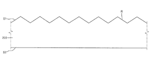
図1及び図2に本発明の一実施形態における光電素子の構造を模式的に図示する。 1 and 2 schematically show the structure of a photoelectric element in one embodiment of the present invention.
図1及び図2を参照すると、本実施形態に係る光電素子は、半導体基板100と、該半導体基板100に交互に形成されたコンタクト層100c及びウィンドウ層100wと、該コンタクト層100c上に形成された第1電極110と、を含む。
1 and 2, the photoelectric device according to the present embodiment is formed on a
半導体基板100は、第1面S1と、第1面S1と対向する第2面S2とを有してもよい。例えば、第1面S1は、半導体基板100の受光面側であり、第2面S2は、受光面に対向する背面側であってもよい。
The
例えば、半導体基板100は、第1面S1からの受光によってキャリアを生成することができる。キャリアとは、第1面S1から受光した光が半導体基板100に吸収されて生成された正孔と電子とを意味する。半導体基板100は、n型またはp型の導電型である単結晶または多結晶シリコン基板などで形成されてもよい。例えば、本発明の一実施形態において、半導体基板100はp型単結晶シリコン基板が用いられてもよい。
For example, the
半導体基板100の第1面S1には、微小な凹凸が形成されてもよい。例えば、半導体基板100の第1面S1には、凹凸パターンを含むテクスチャー(texture)構造Rが形成されてもよい。テクスチャー構造Rは、入射光の反射率を低下させ、できる限り多量の入射光が半導体基板100に吸収されるようにし、光電素子の光収集効率を上昇させる。
Minute irregularities may be formed on the first surface S <b> 1 of the
半導体基板100の第1面S1には、コンタクト層100c及びウィンドウ層100wが形成されてもよい。例えば、半導体基板100の第1面S1に沿って、複数のコンタクト層100c及びウィンドウ層100wが互いに交互に形成されてもよい。図2において、領域Ac及びAwは、それぞれコンタクト層100c及びウィンドウ層100wが形成された領域を示す。
A
コンタクト層100c及びウィンドウ層100wは、半導体基板100とは異なる導電型のドーパントによってドーピングされ、p−n接合を形成することができる。例えば、コンタクト層100c及びウィンドウ層100wは、p型半導体基板100にn型ドーパントを注入し、n型ドーピング層として形成してもよい。コンタクト層100c及びウィンドウ層100wは、同一の導電型ドーパントでドーピングされるが、互いに異なるドーピングレベルで形成される。例えば、コンタクト層100cは、高濃度にドーピングされ、ウィンドウ層100wは、低濃度にドーピングされてもよい。
The
コンタクト層100cは、第1電極110が位置する電極接合部を、選択的に高濃度でドーピングした領域である。コンタクト層100cは、半導体基板100から生成された少数キャリアを収集するエミッタ(emitter)が局所的に形成された選択的エミッタ(selective emitter)を形成する。例えば、コンタクト層100c上に、金属素材の第1電極110を形成し選択的エミッタを形成することができる。また、コンタクト層100cは、電極接合部を高濃度にドーピングすることにより、第1電極110との接触抵抗を低くすることができる。
The
ウィンドウ層100wは、半導体基板100の有効入射面を提供する。ウィンドウ層100wからの光の入射によって、半導体基板100からキャリアが生成される。第1電極110が位置するコンタクト層100cは高濃度にドーピングされ、第1電極110との接触抵抗を減少させるが、第1電極110が位置しないウィンドウ層100wは低濃度にドーピングされる。上記により、半導体基板100の表面に集中した過剰なドーパントによる表面再結合損失を減らすことができるため、表面近くで吸収される光の短波長領域の変換効率を上昇させることができる。
The
コンタクト層100c及びウィンドウ層100wは、ドーピング物質層(図示せず)を全面に塗布した半導体基板100を局所的に加熱することにより、加熱した一部領域に対するドーパントの固溶度及び拡散速度を増大させる方法により形成されてもよい。このとき、局所的に加熱された一部領域は、高濃度にドーピングされたコンタクト層100cを形成することができ、加熱されていない残りの領域は、低濃度にドーピングされたウィンドウ層100wを形成することができる。
The
さらに具体的には、コンタクト層100c及びウィンドウ層100wは、先蒸着(pre−deposition)工程、熱拡散(drive−in)工程、後蒸着(post−deposition)工程、及び局所加熱工程という一連の工程によって形成されてもよい。先蒸着工程及び後蒸着工程の2回の蒸着工程によって、半導体基板100上に、厚膜のドーピング物質層(図示せず)を形成することができる。
More specifically, the
熱拡散工程では、ドーピング物質層のドーパントが、半導体基板100内に拡散するように、高温による熱処理を行う。局所加熱工程では、半導体基板100の選択された一部領域を局所的に加熱し、異なるドーピングレベルを有するコンタクト層100c及びウィンドウ層100wを形成する。
In the thermal diffusion step, heat treatment is performed at a high temperature so that the dopant of the doping material layer is diffused into the
先蒸着工程及び後蒸着工程の2回の蒸着工程を実施することにより、半導体基板100上に、厚膜のドーピング物質層(図示せず)を形成することができ、さらに、局所的に加熱を行うことによりコンタクト層100cのドーピングレベルを上昇させ、高い開放電圧を得ることができる。また、コンタクト層100cと、第1電極110との接触抵抗を減らすことができる。
By performing two deposition processes, a pre-deposition process and a post-deposition process, a thick doping material layer (not shown) can be formed on the
特に、熱拡散工程の前後で、互いに異なる工程条件が適用された先蒸着工程、及び後蒸着工程の2回の蒸着工程を行うことにより、ドーピングレベルを上昇させつつも、従来はドーピングレベルの上昇に伴い生じていた表面再結合損失やキャリア寿命時間の短縮を避けることができる。具体的には、ドーパントの拡散に有利な濃度勾配を形成するように、後蒸着工程は先蒸着工程より高濃度のドーパントソースが使用される。また、先蒸着工程より後蒸着工程の工程時間を短くすることにより、コンタクト層のドーピングレベルを高めつつも、光によって生成されたキャリアを電荷分離するp−n接合の接合深度(junction depth)を浅くすることができ、半導体基板100の表面に過度なドーパントが集中することを阻むことができる。
In particular, before and after the thermal diffusion process, the doping level is raised by performing two deposition processes, a pre-deposition process and a post-deposition process in which different process conditions are applied. Thus, it is possible to avoid the surface recombination loss and the shortening of the carrier life time that have occurred. Specifically, a higher concentration dopant source is used in the post-deposition step than in the pre-deposition step so as to form a concentration gradient that is advantageous for dopant diffusion. In addition, by shortening the post-deposition process time compared to the pre-deposition process, the junction depth of the pn junction that separates charges generated by light while increasing the doping level of the contact layer can be increased. It can be shallow, and excessive dopants can be prevented from concentrating on the surface of the
上記について、比較例1及び比較例2と対比して説明すれば、以下の通りである。 The above will be described in comparison with Comparative Example 1 and Comparative Example 2 as follows.
比較例1では、高いドーピング濃度を得るために、1回の蒸着工程によって、厚膜のドーピング物質層を形成する。比較例1では、半導体基板の表面のドーパント濃度が過度に上昇するため、半導体基板の表面に集中された過剰のドーパントによって、表面再結合速度が増大し、キャリアの寿命時間は短くなる。また、比較例1では、光によって生成されたキャリアを電荷分離するp−n接合の接合深度が増大し、キャリアの収集効率が落ちてしまう。結果的に、開放電圧と短絡電流が低下し、太陽電池の曲線因子(fill factor)及び変換効率が低下してしまう。 In Comparative Example 1, in order to obtain a high doping concentration, a thick doping material layer is formed by a single vapor deposition process. In Comparative Example 1, since the dopant concentration on the surface of the semiconductor substrate is excessively increased, the excess dopant concentrated on the surface of the semiconductor substrate increases the surface recombination rate and shortens the lifetime of carriers. In Comparative Example 1, the junction depth of the pn junction that separates charges generated by light is increased, and the carrier collection efficiency is lowered. As a result, the open circuit voltage and the short circuit current are reduced, and the fill factor and conversion efficiency of the solar cell are reduced.
比較例2では、ドーピング物質層を厚膜に形成する代わりに、半導体基板100のコンタクト層100cに高出力のレーザを照射してドーパントの固溶度を上昇させ、照射領域へのドーパント拡散を促進する。すなわち、比較例2は、ドーピングされた半導体基板の選択された領域(コンタクト層100c)に対してレーザを照射する際に、高出力のレーザを用いることにより、ドーパントの固溶度をさらに上昇させ、拡散をさらに促進する方法である。これによりドーピング物質層を厚膜に形成せずに、高濃度のコンタクト層100cを形成することができる。しかし、比較例2では、高出力のレーザによって半導体基板100の表面が損傷し、半導体基板100の照射領域の抵抗がかえって上昇し、表面再結合損失が増大して太陽電池の曲線因子が低下する。
In Comparative Example 2, instead of forming the doping material layer as a thick film, the
本発明の一実施形態では、後蒸着工程において、先蒸着工程より高濃度のドーパントソースを使用し、かつ先蒸着工程より後蒸着工程の工程時間を短くすることにより、選択的エミッタ(コンタクト層100c)のドーピング濃度は高めつつも、浅い接合深度と低い表面再結合速度とを得ることができる。
In one embodiment of the present invention, a selective emitter (
先蒸着工程及び後蒸着工程の後の局所加熱工程では、均一な濃度にドーピングされた半導体基板100上の選択された領域(コンタクト層100c)を局所的に加熱することにより、ドーピングレベルが互いに異なるウィンドウ層100w及びコンタクト層100cを形成することができる。例えば、レーザの照射領域では、固溶度と拡散速度とが増大するため、ドーピング物質層(図示せず)のドーパントが早く拡散し、ドーピングレベルが上昇する。したがって、レーザ照射領域では、高濃度にドーピングされたコンタクト層100cが形成され、レーザ非照射領域では、低濃度にドーピングされたウィンドウ層100wが形成される。
In the local heating process after the pre-deposition process and the post-deposition process, the selected regions (
レーザの出力は、照射領域に対するドーパントの拡散を促進するのに十分でありつつも、レーザの照射による損傷を引き起こさないほどの出力範囲に設定されることが望ましい。例えば、レーザの出力が過度に設定されている場合、レーザ照射により照射領域の損傷が起きるので、欠陥部分での抵抗が増加し、直列抵抗の上昇及び太陽電池の曲線因子の低下が引き起こされる。 The output of the laser is desirably set to an output range that is sufficient to promote the diffusion of the dopant into the irradiation region but does not cause damage due to the laser irradiation. For example, when the output of the laser is set excessively, the irradiated region is damaged by the laser irradiation, so that the resistance at the defective portion increases, causing an increase in series resistance and a decrease in the fill factor of the solar cell.
コンタクト層100c上には、第1電極110が形成される。第1電極110は、p−n接合を介して電荷分離したキャリアを外部に引き出すことができる。第1電極110は、選択的に高濃度でドーピングされたコンタクト層100cに接続されてもよい。
A
第1電極110は、光電流(photo current)の引き出し方向に沿って、一方向に延びるストライプパターンで形成されてもよい。第1電極110は、銀(Ag)、アルミニウム(Al)、銅(Cu)、ニッケル(Ni)などの金属素材で形成されてもよく、電極ペーストの塗布、乾燥及び焼成(firing)により、コンタクト層100c上にスクリーンプリンティングされてもよい。高濃度にドーピングされたコンタクト層100c上に、第1電極110を接続することにより、コンタクト層100cと、第1電極110との接触抵抗を減らすことができる。
The
半導体基板100の第2面S2には、第2電極120が形成されてもよい。例えば、第2電極120は、半導体基板100上にスクリーンプリンティングされて形成されてもよく、また、第2電極120は多数のキャリアを収集するベース(base)に接続されてもよい。
A
また、半導体基板100の第1面S1及び第2面S2には、それぞれ反射防止膜115及び背面電界層125が形成されてもよい。例えば、反射防止膜115は、相殺的干渉により入射光の反射率を低下させ、入射光の特定波長領域の選択性を増大させる。
Further, an
反射防止膜115は、シリコン酸化膜(例えば、SiO2)やシリコン窒化膜(例えば、Si3N4)の単一層またはこれらの複合層で形成されてもよい。また、反射防止膜115は、熱酸化または化学気相蒸着などの方法により形成されてもよい。
The
背面電界層125は、半導体基板100と同一の導電型であるドーパントの高濃度ドーピング領域として形成されてもよい。背面電界層125は、キャリアの表面再結合損失を抑制するために、高濃度/低濃度の接合を介して、背面電界を形成する。例えば、前記背面電界層125は、p型半導体基板100に形成された高濃度のp+層であってもよい。
The back surface
一方、反射防止膜115及び背面電界層125は、表面再結合損失を減らすためのパッシベーション機能を兼ねることができる。例えば、反射防止膜115及び背面電界層125は、半導体基板100の互いに異なる第1面S1及び第2面S2のパッシベーション膜として機能することができる。
On the other hand, the
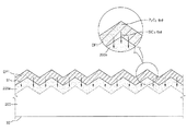
以下、図3A〜図3Mを参照し、本発明の一実施形態による光電素子の製造方法について説明する。 Hereinafter, a method for manufacturing a photoelectric device according to an embodiment of the present invention will be described with reference to FIGS. 3A to 3M.
まず、図3Aに図示するように、半導体基板200を準備する。例えば、半導体基板200は、p型結晶質シリコンウェーハであってもよい。また、例えば、半導体基板200の表面に付着した物理的・化学的不純物を除去するために、酸やアルカリの溶液を用いる洗浄工程が行われてもよい。
First, as shown in FIG. 3A, a
次に、図3Bに図示するように、半導体基板200の第2面S2を覆うエッチング防止膜Mが形成される。後述するように、エッチング防止膜Mは、第1面S1に対する表面テクスチャリング(texturing)時にエッチングマスクの機能を果たす。エッチング防止膜Mは、テクスチャリング・エッチャントに対して耐性を有する素材で形成されていればよい。例えば、前記エッチング防止膜Mは、シリコン酸化膜(例えば、SiO2)やシリコン窒化膜(例えば、Si3N4)で形成されていてもよい。このようなエッチング防止膜Mは、熱酸化によって酸化膜を形成したり、化学気相蒸着(CVD:chemical vapor deposition)によって酸化膜や窒化膜を蒸着したりすることにより形成される。
Next, as shown in FIG. 3B, an etching preventing film M that covers the second surface S2 of the
次に、図3Cに図示するように、半導体基板200の第1面S1に、表面テクスチャリングを行う。例えば、半導体基板200に対して、エッチャントとして水酸化カリウム(KOH)、水酸化ナトリウム(NaOH)のようなアルカリ溶液を適用して異方性エッチングを行い、半導体基板200表面に凹凸パターンを有するテクスチャー構造Rを形成することができる。このとき、エッチング防止膜Mで覆われている半導体基板200の第2面S2は、エッチングされずにエッチング防止膜Mにより保護される。図3Dに図示するように、役割を果たしたエッチング防止膜Mは、除去されてもよい。
Next, as illustrated in FIG. 3C, surface texturing is performed on the first surface S <b> 1 of the
次に、図3E〜図3Iに図示された一連の工程を行い、図3Iに図示されているように、半導体基板200の第1面S1に、コンタクト層200cとウィンドウ層200wとを形成する。コンタクト層200cとウィンドウ層200wは、先蒸着(pre−deposition)工程、熱拡散(drive−in)工程、後蒸着(post−deposition)工程、及び局所加熱工程という一連の工程で形成されてもよい。以下、一連の工程について詳しく説明する。
Next, a series of steps illustrated in FIGS. 3E to 3I are performed to form the
まず、図3Eに図示するように、半導体基板200の第1面S1上に、第1ドーピング物質層DP1を形成する先蒸着工程を行う。先蒸着工程では、p型またはn型のドーピング物質層DP1を形成することができ、例えば、p型半導体基板200と異なる導電型であるn型ドーピング物質層DP1を形成することができる。先蒸着工程には、拡散管(diffusion tube)を利用する拡散システムが適用されてもよい。
First, as illustrated in FIG. 3E, a pre-evaporation process for forming the first doping material layer DP1 on the first surface S1 of the
さらに具体的には、先蒸着工程では、ドーピングソースとしてのPOCl3(オキシ塩化リン)を用い、窒素と酸素とが混合されたキャリアガスによって、拡散管内の半導体基板200上に投入する。このとき、POCl3は、酸素と反応し、P2O5酸化膜となり第1ドーピング物質層DP1を形成する。
More specifically, in the pre-deposition step, POCl 3 (phosphorus oxychloride) as a doping source is used, and is introduced onto the
半導体基板200のシリコンと反応する前の第1ドーピング物質層DP1は、P2O5酸化膜として存在する。シリコンとの反応により、第1ドーピング物質層DP1のドーパントP(リン:phosphorus)は、半導体基板200の内部に拡散し、半導体基板200の表面には、酸化物が成長する。このとき、第1ドーピング物質層DP1は、SiO2を含むガラス層(PSG:phosphosilicate glass)となる。
The first doping material layer DP1 before reacting with silicon of the
また、先蒸着時のPOCl3の濃度は、ほぼ5〜7%の範囲で選択されることが望ましい。下限値(5%)より低い濃度のドーピングソースが適用される場合、半導体基板のドーパントの表面濃度が十分ではなく、電極との接触抵抗が上昇する。また、上限値(7%)より高い濃度のドーピングソースが適用される場合、半導体基板200のドーパントの表面濃度が過度に上昇して表面再結合損失が増大する。具体的には、先蒸着工程の工程条件として、5.7%濃度のPOCl3をドーピングソースとして使用し、800℃〜900℃で、10分〜20分間蒸着することが望ましい。さらに具体的には、先蒸着工程は、840℃の温度で15分間行われてもよい。
Further, the concentration of POCl 3 at the time of pre-deposition is preferably selected within a range of about 5 to 7%. When a doping source having a concentration lower than the lower limit (5%) is applied, the surface concentration of the dopant of the semiconductor substrate is not sufficient, and the contact resistance with the electrode increases. Further, when a doping source having a concentration higher than the upper limit (7%) is applied, the surface concentration of the dopant of the
ここで、本明細書におけるPOCl3濃度は、半導体基板200が置かれた蒸着チャンバ(例えば、拡散管)内に投入される全体ガス(キャリアガスを含む全体ガス)においてのPOCl3の占める体積流量を示す。例えば、5.7%濃度のPOCl3とは、16slm(標準状態流量(standard litters per minute:slm)0℃、1atmにおける1分間当たりの流量をリットル単位で表示した単位)の窒素、0.5slmの酸素、1slmのPOCl3を含む総17.5slmの全体ガスにおいて、POCl3の体積流量が5.7%であることを示す。
Here, the POCl 3 concentration in this specification is the volume flow rate occupied by POCl 3 in the entire gas (the entire gas including the carrier gas) introduced into the vapor deposition chamber (for example, the diffusion tube) in which the
次に、図3Fに図示するように、第1ドーピング物質層DP1のドーパントが半導体基板200内に速かに拡散するように、熱拡散(drive−in)工程を行う。熱拡散工程では、ドーピング物質を追加注入せずに、拡散管内の半導体基板200を高い温度に維持する。熱拡散工程は、先蒸着工程と共に連続でなされ、先蒸着工程を行った拡散管内で一括してなされる。熱拡散工程の工程条件として、不活性雰囲気下、800℃〜900℃で、30分〜50分間を用いてもよい。また、具体的な一例として、熱拡散工程は、840℃で40分間行われてもよく、窒素ガスなどの不活性ガスが注入されてもよい。
Next, as illustrated in FIG. 3F, a thermal diffusion (drive-in) process is performed so that the dopant of the first doping material layer DP <b> 1 is quickly diffused into the
これにより、第1ドーピング物質層DP1のドーパントP(リン:phosphorus)は、半導体基板200に拡散していき、半導体基板200の表面には、n型エミッタ層200eが形成される。拡散の進行により、P2O5のドーパントP(リン:phosphorus)は、半導体基板200の内部に拡散していき、半導体基板200の表面では、酸化物が成長する。第1ドーピング物質層DP1は、厚み方向に沿って、上部が相対的に高いP2O5含量を有し、下部が相対的に高いSiO2含量を有し、連続的に変化する濃度勾配を有するようになる。ここで、特許請求の範囲の記載では、熱拡散は、単に拡散と表現される。
Accordingly, the dopant P (phosphorus) of the first doping material layer DP1 diffuses into the
次に、図3Gに図示するように、第1ドーピング物質層DP1上に、第2ドーピング物質層DP2を形成する後蒸着工程(post−deposition)が行われる。後蒸着工程では、第1ドーピング物質層DP1と同一の導電型である第2ドーピング物質層DP2を形成することができる。また、蒸着チャンバとして、拡散管(diffusion tube)を利用する拡散システムが適用されてもよい。 Next, as illustrated in FIG. 3G, a post-deposition process for forming the second doping material layer DP2 on the first doping material layer DP1 is performed. In the post-deposition process, the second doping material layer DP2 having the same conductivity type as the first doping material layer DP1 can be formed. In addition, a diffusion system using a diffusion tube may be applied as the deposition chamber.
具体的には、後蒸着工程では、ドーピングソースとしてPOCl3(オキシ塩化リン)を、窒素と酸素とを混合したキャリアガスを用いて、拡散管内の半導体基板200上に投入する。
Specifically, in the post-deposition step, POCl 3 (phosphorus oxychloride) is introduced as a doping source onto the
後蒸着工程の工程条件は、先蒸着工程と異なってもよい。すなわち、後蒸着工程では、先蒸着工程より高濃度のドーピングソースを使い、先蒸着工程より短い工程時間を適用する。このように、先蒸着工程より高濃度のドーピングソースを使うことにより、第2ドーピング物質層DP2から半導体基板200に向けて、拡散に有利な濃度勾配を形成することができる。また、相対的に短い工程時間を適用することで、半導体基板200の表面濃度及び接合深度が増大することを抑制することができる。
The process conditions of the post-deposition process may be different from the pre-deposition process. That is, in the post-deposition process, a higher concentration doping source is used than in the pre-deposition process, and a shorter process time is applied than in the pre-deposition process. As described above, by using a doping source having a higher concentration than in the pre-deposition step, a concentration gradient advantageous for diffusion can be formed from the second doping material layer DP2 toward the
すなわち、先蒸着工程時のドーピングソースの第1濃度Co1及び第1工程時間t1と、後蒸着工程時のドーピングソースの第2濃度Co2及び第2工程時間t2とを比較すると、第1濃度Co1より第2濃度Co2のほうが大きく(Co1<Co2)、第1工程時間t1より第2工程時間t2のほうが短い(t1>t2)。 That is, when the first concentration Co1 and the first process time t1 of the doping source in the pre-deposition process are compared with the second concentration Co2 and the second process time t2 of the doping source in the post-deposition process, the first concentration Co1 The second concentration Co2 is larger (Co1 <Co2), and the second process time t2 is shorter than the first process time t1 (t1> t2).
例えば、後蒸着工程のPOCl3濃度は、おおよそ10%以上、さらに望ましくは、おおよそ12%以上としてもよい。10%より低い濃度のドーピングソースでは、先蒸着工程より高い濃度勾配、すなわち、ドーパント拡散に有利な濃度勾配を形成することができなくなる。ここで、本明細書においてPOCl3濃度は、半導体基板200が置かれた蒸着チャンバ(例えば、拡散管)中に投入される全体ガス(キャリアガスを含む全体ガス)中で、POCl3の占める体積流量を示す。
For example, the POCl 3 concentration in the post-deposition step may be approximately 10% or more, more desirably approximately 12% or more. With a doping source having a concentration lower than 10%, it is impossible to form a higher concentration gradient than that of the pre-deposition process, that is, a concentration gradient advantageous for dopant diffusion. Here, in this specification, the POCl 3 concentration is the volume occupied by POCl 3 in the entire gas (the entire gas including the carrier gas) introduced into the vapor deposition chamber (for example, the diffusion tube) in which the
具体的には、後蒸着工程の条件は、12.5%濃度のPOCl3をドーピングソースとして使用し、800℃〜900℃で、3分〜8分間としてもよい。具体的な一例として、後蒸着工程は、840℃で5分間行われる。 Specifically, the conditions of the post-deposition process may be 12.5% POCl 3 as a doping source, 800 ° C. to 900 ° C. and 3 minutes to 8 minutes. As a specific example, the post-deposition process is performed at 840 ° C. for 5 minutes.
また、ドーパント拡散前の第2ドーピング物質層DP2は、P2O5酸化膜として存在する。第2ドーピング物質層DP2のドーパントが、半導体基板200内部に拡散していくことにより、半導体基板200の表面には、酸化物が成長する。このとき、第2ドーピング物質層DP2は、SiO2を含むガラス層(PSG)となることができる。
In addition, the second doping material layer DP2 before the dopant diffusion exists as a P 2 O 5 oxide film. As the dopant of the second doping material layer DP2 diffuses into the
ここで第2ドーピング物質層DP2は、先蒸着された第1ドーピング物質層DP1と共に、厚膜のガラス層(PSG)を形成することができる。すなわち、第2ドーピング物質層DP2は、第1ドーピング物質層DP1と共に、所定の膜厚tを有する1層のガラス層(PSG)を形成する。このとき、該ガラス層(PSG)は、半導体基板200の界面付近で酸化膜が成長し、相対的に高いSiO2含量を有する。すなわち、ガラス層(PSG)は、半導体基板200の界面から遠くなるにつれ、SiO2含量はだんだんと小さくなり、P2O5含量は、だんだんと大きくなる濃度プロファイルを有してもよい。例えば、第1ドーピング物質層DP1及び第2ドーピング物質層DP2のシリコン酸化物の濃度は、半導体基板200に近づくほど上昇する。
Here, the second doping material layer DP2 may form a thick glass layer (PSG) together with the pre-deposited first doping material layer DP1. That is, the second doping material layer DP2 forms a single glass layer (PSG) having a predetermined thickness t together with the first doping material layer DP1. At this time, in the glass layer (PSG), an oxide film grows near the interface of the
次に、図3Hに図示するように、第1ドーピング物質層DP1及び第2ドーピング物質層DP2が形成された半導体基板200上のコンタクト領域Acを局所的に加熱し、ドーピングレベルが異なる領域を作製する局所加熱工程が行われる。局所加熱工程では、半導体基板200上の一部領域、さらに具体的には、第1電極210を形成するコンタクト領域Acを局所的に加熱し、高濃度のコンタクト層200cを形成する。
Next, as illustrated in Figure 3H, the contact area A c of the
半導体基板200上のコンタクト領域Acに対してレーザLを照射することにより、コンタクト領域Acの固溶度及び拡散速度が増大する。すなわち、先蒸着工程及び後蒸着工程によって、厚膜に形成されたドーピング物質層DP1、DP2のドーパントP(リン:phosphorus)が、レーザLを照射したコンタクト領域Ac内に拡散し、ドーピング濃度が上昇する。
By irradiating the laser L with respect to the contact area A c of the
このとき、レーザLを照射したコンタクト領域Acには、高いドーピングレベルを有するコンタクト層200cが形成され、レーザLを照射しないウィンドウ領域Awには、相対的に低いドーピングレベルを有するウィンドウ層200wが形成される。照射されたレーザLは、高いバンドギャップ・エネルギー(band−gap energy)を有する第1ドーピング物質層DP1及び第2ドーピング物質層DP2には吸収されることなく透過し、半導体基板200に吸収されてドーパントP(リン:phosphorus)の固溶度及び拡散を促進する。
In this case, the laser L contact area A c irradiated with is formed a
本発明の一実施形態では、先蒸着工程及び後蒸着工程の2回蒸着工程を行うので、1回蒸着と比較すると、より厚膜のドーピング物質層DP1、DP2を形成することができ、局所加熱工程によって、より高濃度のコンタクト層200cを形成することができる。コンタクト層200cのドーピング濃度を高めることにより、第1電極110との接触抵抗が低下し、さらに光電流の直列抵抗が低減することによって、高い開放電圧を得ることができ、曲線因子が上昇する。ここで、特許請求の範囲の記載では、局所加熱は、選択的拡散と表現した。また、選択的拡散と対比して、熱拡散は、拡散と表現した。
In one embodiment of the present invention, since the pre-evaporation process and the post-evaporation process are performed twice, the thicker doping material layers DP1 and DP2 can be formed compared to the single deposition process. A higher
次に、図3H及び図3Iに図示するように、第1ドーピング物質層DP1及び第2ドーピング物質層DP2を除去するエッチバック(etch−back)が行われる。第1ドーピング物質層DP1及び第2ドーピング物質層DP2は、ガラス層(PSG)状態で存在し、半導体基板200に内包された金属の不純成分の析出物を含んでいるため、これを除去することにより、不純成分を除去するギャザリング(gathering)効果を期待することもできる。
Next, as illustrated in FIGS. 3H and 3I, etch-back is performed to remove the first doping material layer DP1 and the second doping material layer DP2. Since the first doping material layer DP1 and the second doping material layer DP2 exist in a glass layer (PSG) state and contain precipitates of impure components of metal included in the
例えば、第1ドーピング物質層DP1及び第2ドーピング物質層DP2は、酸性溶液のエッチャントを適用してエッチング除去されてもよく、硝酸(HNO3)及びフッ酸(HF)と、酢酸(CH3COOH)または脱イオン水(DI water)との混合溶液を適用することができる。ただし、本発明の変形例として、このような第1ドーピング物質層DP1及び第2ドーピング物質層DP2を除外せずに、パッシベーション膜として活用してもよい。 For example, the first doping material layer DP1 and the second doping material layer DP2 may be etched away by applying an etchant of an acidic solution, such as nitric acid (HNO 3 ), hydrofluoric acid (HF), and acetic acid (CH 3 COOH). ) Or a mixed solution with deionized water (DI water). However, as a modification of the present invention, the first doping material layer DP1 and the second doping material layer DP2 may be used as a passivation film without being excluded.
次に、図3Jに図示するように、半導体基板200の第1面S1上に、反射防止膜215を形成する。例えば、反射防止膜215は、シリコン酸化膜(例えば、SiO2)、シリコン窒化膜(例えば、Si3N4)、水素化されたシリコン窒化膜(SiN:H)などで形成してもよい。また、シリコン酸化膜の単一層で形成されてもよく、あるいは互いに屈折率が異なるシリコン酸化膜とシリコン窒化膜との複合層で形成されてもよい。さらに、反射防止膜215は、化学気相蒸着(CVD)を利用して形成されてもよい。
Next, as illustrated in FIG. 3J, an
反射防止膜215は、半導体基板200で生成されたキャリアの表面再結合を防止し、キャリアの収集効率を向上させるパッシベーション膜の役目を兼ねることができる。すなわち、反射防止膜215は、半導体基板200の表面に存在するシリコン原子の未結合状態(dangling bond)によるキャリアの捕獲(trapping)を防止し、キャリアの収集効率を向上させることができる。
The
次に、図3Kに図示するように、コンタクト層200c上に、第1電極210を形成する。第1電極210は、光電流の引き出し方向に沿って、一方向に並んで延びるストライプパターンで形成されてもよく、また光の有効入射面積を考慮したパターンで形成されてもよい。
Next, as illustrated in FIG. 3K, the
第1電極210は、銀(Ag)、アルミニウム(Al)、銅(Cu)、ニッケル(Ni)などの金属素材を含んでもよい。例えば、スクリーンプリンティングを利用し、コンタクト層200c上に電極ペースト(図示せず)をパターン印刷した後、乾燥及び焼成してもよい。係る場合、電極ペースト(図示せず)に含まれたガラスフリット成分が反射防止膜215を貫くことにより、第1電極210とコンタクト層200cとを互いに接触させることができる。
The
次に、図3Lに図示するように、半導体基板200の第2面S2上に、背面電界(BSF:back surface field)層225を形成する。例えば、背面電界層225は、高濃度ドーピング層で形成されてもよく、半導体基板200と同一導電型のドーパントを高濃度でドーピングして形成してもよい。例えば、背面電界層225は、p型半導体基板200の第2面S2に高濃度p+層として形成されてもよい。係る構成により、背面電界層225は、少数キャリア(電子)が第2面S2側に移動して再結合することを防止することができる。
Next, as illustrated in FIG. 3L, a back surface field (BSF)
次に、図3Mに図示するように、半導体基板200の第2面S2上に、第2電極220が形成される。第2電極220は、銀(Ag)、アルミニウム(Al)、銅(Cu)、ニッケル(Ni)などの金属素材で形成されてもよい。また、第2電極220は、スクリーンプリンティングやメッキのような方法で形成されてもよい。例えば、第2電極220は、電極ペースト(図示せず)の塗布後、乾燥及び焼成により形成されてもよく、第1電極ペースト(図示せず)と第2電極ペースト(図示せず)とを共に焼成する工程(co−firing)により、第1面S1上の第1電極210と、第2面S2上の第2電極220とを共に形成してもよい。
Next, as illustrated in FIG. 3M, the second electrode 220 is formed on the second surface S <b> 2 of the
以下の表1に本発明による光電素子の特性を評価するための実験結果を示す。 Table 1 below shows experimental results for evaluating the characteristics of the photoelectric device according to the present invention.

比較例3〜6は、先蒸着工程及び熱拡散工程によりコンタクト層を形成した光電素子を示し、実施例は、コンタクト層を本発明の実施形態によって形成した光電素子を示す。 Comparative Examples 3 to 6 show photoelectric elements in which a contact layer is formed by a pre-deposition process and a thermal diffusion process, and Examples show photoelectric elements in which a contact layer is formed according to an embodiment of the present invention.
比較例3では、4.7%濃度のPOCl3をドーピングソースにして、840℃で15分間、先蒸着工程を行い、その後840℃の温度で40分間、熱拡散工程を行った。 In Comparative Example 3, a pre-evaporation process was performed at 840 ° C. for 15 minutes using 4.7% concentration of POCl 3 as a doping source, and then a thermal diffusion process was performed at a temperature of 840 ° C. for 40 minutes.
比較例4では、8.7%濃度のPOCl3をドーピングソースにして、840℃で25分間、先蒸着工程を行い、その後830℃の温度で20分間、熱拡散工程を行った。 In Comparative Example 4, a pre-deposition process was performed at 840 ° C. for 25 minutes using 8.7% concentration of POCl 3 as a doping source, and then a thermal diffusion process was performed at a temperature of 830 ° C. for 20 minutes.
比較例5では、8.7%濃度のPOCl3をドーピングソースにして、840℃で15分間、先蒸着工程を行い、その後840℃の温度で15分間、熱拡散工程を行った。 In Comparative Example 5, a pre-deposition process was performed at 840 ° C. for 15 minutes using 8.7% concentration of POCl 3 as a doping source, and then a thermal diffusion process was performed at a temperature of 840 ° C. for 15 minutes.
比較例6では、12.5%濃度のPOCl3をドーピングソースにして、840℃で10分間、先蒸着工程を行い、その後840℃の温度で15分間、熱拡散工程を行った。 In Comparative Example 6, a pre-deposition process was performed at 840 ° C. for 10 minutes using POCl 3 having a concentration of 12.5% as a doping source, and then a thermal diffusion process was performed at a temperature of 840 ° C. for 15 minutes.
実施例では、5.7%濃度のPOCl3をドーピングソースにして、840℃で15分間、先蒸着工程を行い、その後840℃の温度で40分間、熱拡散工程を行った後、12.5%濃度のPOCl3をドーピングソースにして、840℃で5分間、後蒸着工程を行った。 In the embodiment, a pre-deposition process is performed at 840 ° C. for 15 minutes using 5.7% concentration of POCl 3 as a doping source, and then a thermal diffusion process is performed at a temperature of 840 ° C. for 40 minutes. A post-deposition process was performed at 840 ° C. for 5 minutes using% concentration of POCl 3 as a doping source.
比較例3〜6及び実施例それぞれの場合に、ドーピング物質層の厚みを測定し、コンタクト層の面抵抗と、暗示開放電圧(implied open circuit voltage:implied Voc)を測定した。このとき、コンタクト層の面抵抗は、エッチバックによって、ウィンドウ層100wの面抵抗を110Ω/sqで一致させた同一条件の下で測定した。
In each of Comparative Examples 3 to 6 and Examples, the thickness of the doping material layer was measured, and the surface resistance of the contact layer and the implied open circuit voltage (implied Voc) were measured. At this time, the surface resistance of the contact layer was measured under the same condition in which the surface resistance of the
実施例と比較例3とを比較すると、実施例は比較例3より、さらに厚いドーピング物質層(ガラス層(PSG))を形成することができる。相対的に厚膜のドーピング物質層を形成することにより、ドーパントの添加量を増加させ、コンタクト層のドーピングレベルを高めることができる。 When Example and Comparative Example 3 are compared, the Example can form a thicker doping material layer (glass layer (PSG)) than Comparative Example 3. By forming a relatively thick doping material layer, the amount of dopant added can be increased and the doping level of the contact layer can be increased.
実施例と比較例4、5と比較すると、実施例より厚いドーピング物質層を形成した比較例4、5より、実施例はさらに低いコンタクト層面抵抗を得ることができる。単にドーピング物質層を厚く形成するよりは、実施例のように、後蒸着工程において、相対的に先蒸着工程より高濃度のドーピングソースを適用することにより、ドーパント拡散に有利な濃度勾配を形成することができ、ドーピングレベルを高めるのに効果的であるということが分かる。 Compared with the examples and comparative examples 4 and 5, the examples can obtain lower contact layer surface resistance than the comparative examples 4 and 5 in which the doping material layer thicker than the examples is formed. Rather than simply forming a thick doping material layer, a concentration gradient advantageous for dopant diffusion is formed in the post-deposition process by applying a higher concentration of doping source than in the pre-deposition process, as in the embodiment. It can be seen that it is effective to increase the doping level.
同一濃度のドーピングソース(12.5%、POCl3)を適用した実施例と比較例6とを比較すると、比較例6より、実施例はさらに低いコンタクト層面抵抗が得られる。単にドーピングソースの濃度を高めるより、実施例のように、後蒸着工程において、相対的に先蒸着工程より高濃度のドーピングソースを適用することにより、ドーパント拡散に有利な濃度勾配を形成することができ、ドーピングレベルを高めるのに効果的であるということが分かる。 Comparing the example using the same concentration doping source (12.5%, POCl 3 ) with the comparative example 6, the contact layer surface resistance of the example is lower than that of the comparative example 6. Rather than simply increasing the concentration of the doping source, a concentration gradient advantageous for dopant diffusion can be formed in the post-deposition process by applying a higher concentration of the doping source than in the pre-deposition process, as in the embodiment. It can be seen that it is effective in increasing the doping level.
比較例3〜6及び実施例で、暗示開放電圧(implied Voc)を測定した結果から、実施例は最も高い暗示開放電圧を得る可能性があるということを確認することができる。暗示開放電圧は、光によって生成されたキャリアの再結合損失を反映し、暗示開放電圧は、再結合損失が増加すると減少する。具体的には、暗示開放電圧は、PCD(photo conductance decay)を利用して測定され、測定されたキャリアの寿命時間を利用して計算される。そのため、キャリアの寿命時間が長いほど、暗示開放電圧値は増大し、実際に製作された光電素子の開放電圧(open circuit voltage:Voc)が増大すると予測される。 From the result of measuring the implicit open circuit voltage (implied Voc) in the comparative examples 3 to 6 and the example, it can be confirmed that the example has a possibility of obtaining the highest implicit open circuit voltage. The implicit open circuit voltage reflects the recombination loss of carriers generated by light, and the implicit open circuit voltage decreases as the recombination loss increases. Specifically, the implicit open circuit voltage is measured using PCD (photo conductance decay), and is calculated using the measured carrier lifetime. For this reason, the longer the lifetime of the carrier, the higher the implicit open circuit voltage value, and the open circuit voltage (open circuit voltage: Voc) of the actually manufactured photoelectric element is expected to increase.
本発明で最も高い暗示開放電圧を得たことは、すなわち半導体基板の表面に直接行われる先蒸着工程で、相対的に低濃度のドーピングソースを適用し、後蒸着工程において先蒸着工程より短縮された工程時間を適用することにより、半導体基板の表面濃度を抑制して表面再結合損失を低下させ、浅い接合深度を形成してキャリア収集効率が向上した結果であると理解される。 In the present invention, the highest implicit open-circuit voltage was obtained, that is, in the pre-deposition process performed directly on the surface of the semiconductor substrate, a relatively low concentration doping source was applied, and the post-deposition process was shortened compared to the pre-deposition process. It is understood that this is a result of suppressing the surface concentration of the semiconductor substrate and reducing the surface recombination loss, forming a shallow junction depth, and improving the carrier collection efficiency by applying the above process time.
比較例3より先蒸着工程のPOCl3濃度を増加させた比較例4〜6で、比較例3より低い面抵抗を得ることは可能であるが、接合深度の増大及び再結合損失の増加により、比較例3よりは暗示開放電圧は低下する。 In Comparative Examples 4 to 6 in which the POCl 3 concentration in the pre-deposition step is increased from that of Comparative Example 3, it is possible to obtain a lower surface resistance than that of Comparative Example 3. The implicit open circuit voltage is lower than in Comparative Example 3.
一方、本発明の一実施形態では、互いに異なる工程条件である先蒸着工程及び後蒸着工程の2回蒸着を適用しているが、本発明は、上記実施形態に限定されない。ドーパントの拡散に有利な濃度勾配を形成するために、後蒸着工程にて先蒸着工程より高濃度のドーピングソースを適用し、接合深度及び表面濃度の過度な上昇を抑制するために、後蒸着工程で、先蒸着工程より相対的に短い工程時間適用されるならば、3回以上蒸着工程が行われてもよい。 On the other hand, in one embodiment of the present invention, two depositions of a pre-deposition process and a post-deposition process, which are different process conditions, are applied, but the present invention is not limited to the above-described embodiment. In order to form a concentration gradient advantageous for dopant diffusion, a post-deposition process is performed in order to suppress an excessive increase in junction depth and surface concentration by applying a higher concentration doping source in the post-deposition process than in the pre-deposition process. In this case, the deposition process may be performed three or more times if the process time is relatively shorter than the previous deposition process.
例えば、3回以上の蒸着を行う場合には、一次蒸着工程、熱拡散工程、二次蒸着工程、熱拡散工程、三次蒸着工程の一連の工程を行うようにしてもよい。係る場合、一次蒸着時のドーピングソースの濃度Co1、二次蒸着時のドーピングソースの濃度Co2、及び三次蒸着時のドーピングソースの濃度Co3は、Co1<Co2<Co3の関係を有してもよい。また、一次蒸着時の工程時間t1、二次蒸着時の工程時間t2、及び三次蒸着時の工程時間t3は、t1>t2>t3の関係を有してもよい。 For example, when performing vapor deposition three or more times, you may make it perform a series of processes, a primary vapor deposition process, a thermal diffusion process, a secondary vapor deposition process, a thermal diffusion process, and a tertiary vapor deposition process. In this case, the concentration Co1 of the doping source during the primary deposition, the concentration Co2 of the doping source during the secondary deposition, and the concentration Co3 of the doping source during the tertiary deposition may have a relationship of Co1 <Co2 <Co3. Moreover, the process time t1 at the time of primary vapor deposition, the process time t2 at the time of secondary vapor deposition, and the process time t3 at the time of tertiary vapor deposition may have a relationship of t1> t2> t3.
上記にて詳述したように、本発明によれば、電極接合部を形成する選択的エミッタ領域を高濃度にドーピングして電極の接触抵抗を低下させ、光電流パスの直列抵抗を下げつつも、ドーピングレベルの上昇に伴う接合深度の増大及びキャリアの表面濃度の過度な上昇による表面再結合損失を抑制することができる光電素子を製造することが可能である。 As described in detail above, according to the present invention, the selective emitter region forming the electrode junction is heavily doped to reduce the contact resistance of the electrode while reducing the series resistance of the photocurrent path. It is possible to manufacture a photoelectric device that can suppress surface recombination loss due to an increase in junction depth accompanying an increase in doping level and an excessive increase in the surface concentration of carriers.
以上、添付図面を参照しながら本発明の好適な実施形態について詳細に説明したが、本発明はかかる例に限定されない。本発明の属する技術の分野における通常の知識を有する者であれば、特許請求の範囲に記載された技術的思想の範疇内において、各種の変更例または修正例に想到し得ることは明らかであり、これらについても、当然に本発明の技術的範囲に属するものと了解される。従って、本発明の真の保護範囲は、特許請求の範囲によって定められる。 The preferred embodiments of the present invention have been described in detail above with reference to the accompanying drawings, but the present invention is not limited to such examples. It is obvious that a person having ordinary knowledge in the technical field to which the present invention pertains can come up with various changes or modifications within the scope of the technical idea described in the claims. Of course, it is understood that these also belong to the technical scope of the present invention. Therefore, the true protection scope of the present invention is defined by the claims.
本発明の光電素子の製造方法は、例えば、太陽電池関連の技術分野に効果的に適用可能である。 The method for producing a photoelectric element of the present invention can be effectively applied to, for example, a technical field related to solar cells.
100、200 半導体基板
100c、200c コンタクト層
100w、200w ウィンドウ層
110、210 第1電極
115、215 反射防止膜
120、220 第2電極
125、225 背面電界層
200e エミッタ層
Ac コンタクト領域
Aw ウィンドウ領域
L レーザ
M エッチング防止膜
R テクスチュア構造
S1 半導体基板の第1面
S2 半導体基板の第2面
DP1 第1ドーピング物質層
DP2 第2ドーピング物質層
t 第1ドーピング物質層及び第2ドーピング物質層が形成するガラス層の厚み
100, 200 semiconductor substrate
100c,
Claims (14)
前記第1ドーピング物質層が形成された前記半導体基板を加熱する熱拡散段階と、
前記熱拡散段階後、前記第1ドーピング物質層上に、前記第2導電型を有する第2ドーピング物質層を形成する後蒸着段階と、
前記半導体基板、前記第1ドーピング物質層及び前記第2ドーピング物質層の一部をレーザで局所加熱し、前記半導体基板の第1面上にコンタクト層を形成する局所加熱段階と、
前記局所加熱段階後、前記第1ドーピング物質層及び第2ドーピング物質層を除去する段階と、
前記コンタクト層上に第1電極を形成し、前記半導体基板の前記第1面と対向する第2面上に第2電極を形成する段階と、
を含み、
前記後蒸着段階は、前記先蒸着段階よりも工程時間が短く、
前記先蒸着段階は、前記半導体基板が存在する蒸着チャンバ内に、POCl 3 を含む第1ドーピングソースを提供する段階を含み、前記後蒸着段階は、前記蒸着チャンバ内に、POCl 3 を含む第2ドーピングソースを提供する段階を含むことを特徴とする光電素子の製造方法。 A pre-deposition step of forming a first doping material layer having a second conductivity type different from the first conductivity type on a semiconductor substrate having a first conductivity type;
A thermal diffusion step of heating the semiconductor substrate on which the first doping material layer is formed;
A post-deposition step of forming a second doping material layer having the second conductivity type on the first doping material layer after the thermal diffusion step;
A local heating step of locally heating a portion of the semiconductor substrate, the first doping material layer, and the second doping material layer with a laser to form a contact layer on the first surface of the semiconductor substrate;
Removing the first doping material layer and the second doping material layer after the local heating step;
Forming a first electrode on the contact layer and forming a second electrode on a second surface opposite to the first surface of the semiconductor substrate;
Only including,
The post-deposition stage is shorter in process time than the pre-deposition stage,
The pre-deposition step may include providing a first doping source including POCl 3 in a deposition chamber in which the semiconductor substrate is present , and the post-deposition step may include a second step including POCl 3 in the deposition chamber. A method for manufacturing a photoelectric device comprising providing a doping source .
前記第2ドーピングソースを提供する段階は、第2工程時間の間行われ、
前記第1工程時間は、前記第2工程時間より長いことを特徴とする請求項1に記載の光電素子の製造方法。 Providing the first doping source is performed for a first process time;
Providing the second doping source is performed for a second process time;
The method for manufacturing a photoelectric device according to claim 1 , wherein the first process time is longer than the second process time.
前記第2ドーピングソースを提供する段階では、前記第2ドーピングソースは、キャリアガスを介して供給され、前記第2ドーピングソースは第2濃度を有し、
前記第2濃度は、前記第1濃度より高いことを特徴とする請求項1又は2に記載の光電素子の製造方法。 In providing the first doping source, the first doping source is supplied through a carrier gas, and the first doping source has a first concentration.
In providing the second doping source, the second doping source is supplied via a carrier gas, and the second doping source has a second concentration.
The method for manufacturing a photoelectric device according to claim 1, wherein the second concentration is higher than the first concentration.
前記第1ドーピングソースは、キャリアガスを介して供給され、前記第1ドーピングソースは5体積%〜7体積%の濃度を有することを特徴とする請求項1〜3のいずれか一項に記載の光電素子の製造方法。 Providing the first doping source comprises:
The first doping source is supplied through the carrier gas, according to claim 1, characterized in that it comprises a first doping source concentration of 5 vol% to 7 vol% A method for manufacturing a photoelectric element.
前記第2ドーピングソースは、キャリアガスを介して供給され、前記第2ドーピングソースは10体積%以上の濃度を有することを特徴とする請求項1〜5のいずれか一項に記載の光電素子の製造方法。 Providing the second doping source;
6. The photoelectric device according to claim 1 , wherein the second doping source is supplied via a carrier gas, and the second doping source has a concentration of 10% by volume or more. Production method.
前記半導体基板の前記第1面に、前記コンタクト層より低いドーピング濃度を有し、前記コンタクト層と接するウィンドウ層を形成することを特徴とする請求項1〜9のいずれか一項に記載の光電素子の製造方法。 In the local heating step,
The photoelectric layer according to any one of claims 1 to 9 , wherein a window layer having a lower doping concentration than the contact layer and in contact with the contact layer is formed on the first surface of the semiconductor substrate. Device manufacturing method.
前記第1ドーピング物質層のドーパントを前記半導体基板に拡散させ、前記半導体基板の第1面にエミッタ層を形成する拡散段階と、
前記拡散段階後、前記第2導電型を有する第2ドーピング物質層を形成する後蒸着段階と、
前記第1ドーピング物質層及び前記第2ドーピング物質層のドーパントを前記エミッタ層に拡散させ、前記半導体基板の前記第1面の一部にコンタクト層を形成する選択的拡散段階と、
前記選択的拡散段階後、前記第1ドーピング物質層及び第2ドーピング物質層を除去する段階と、
を含み、
前記後蒸着段階後、前記第1ドーピング物質層と前記第2ドーピング物質層は、変化する濃度勾配を有し、前記第1ドーピング物質層及び前記第2ドーピング物質層のシリコン酸化物の濃度は、前記半導体基板に近づくほど上昇し、
前記後蒸着段階は、前記先蒸着段階よりも工程時間が短く、
前記先蒸着段階は、前記半導体基板が存在する蒸着チャンバ内に、POCl 3 を含む第1ドーピングソースを提供する段階を含み、前記後蒸着段階は、前記蒸着チャンバ内に、POCl 3 を含む第2ドーピングソースを提供する段階を含むことを特徴とする光電素子の製造方法。 A pre-deposition step of forming a first doping material layer having a second conductivity type different from the first conductivity type on a first conductivity type semiconductor substrate;
A diffusion step of diffusing the dopant of the first doping material layer into the semiconductor substrate and forming an emitter layer on the first surface of the semiconductor substrate;
A post-deposition step of forming a second doping material layer having the second conductivity type after the diffusion step ;
A selective diffusion step of diffusing the dopants of the first and second doping material layers into the emitter layer to form a contact layer on a portion of the first surface of the semiconductor substrate;
Removing the first and second doping material layers after the selective diffusion step;
Including
After the post-deposition step, the first doping material layer and the second doping material layer have a varying concentration gradient, and the concentration of silicon oxide in the first doping material layer and the second doping material layer is: It rises as it approaches the semiconductor substrate,
The post-deposition stage is shorter in process time than the pre-deposition stage,
The pre-deposition step may include providing a first doping source including POCl 3 in a deposition chamber in which the semiconductor substrate is present , and the post-deposition step may include a second step including POCl 3 in the deposition chamber. A method for manufacturing a photoelectric device comprising providing a doping source .
Applications Claiming Priority (4)
| Application Number | Priority Date | Filing Date | Title |
|---|---|---|---|
| US201161546642P | 2011-10-13 | 2011-10-13 | |
| US61/546642 | 2011-10-13 | ||
| US13/568,462 US8664015B2 (en) | 2011-10-13 | 2012-08-07 | Method of manufacturing photoelectric device |
| US13/568462 | 2012-08-07 |
Publications (2)
| Publication Number | Publication Date |
|---|---|
| JP2013089955A JP2013089955A (en) | 2013-05-13 |
| JP6258576B2 true JP6258576B2 (en) | 2018-01-10 |
Family
ID=46963476
Family Applications (1)
| Application Number | Title | Priority Date | Filing Date |
|---|---|---|---|
| JP2012219627A Active JP6258576B2 (en) | 2011-10-13 | 2012-10-01 | Method for manufacturing photoelectric device |
Country Status (5)
| Country | Link |
|---|---|
| US (1) | US8664015B2 (en) |
| EP (1) | EP2581950A3 (en) |
| JP (1) | JP6258576B2 (en) |
| KR (1) | KR20130040125A (en) |
| CN (1) | CN103050568A (en) |
Families Citing this family (18)
| Publication number | Priority date | Publication date | Assignee | Title |
|---|---|---|---|---|
| DE102010054370A1 (en) * | 2010-12-13 | 2012-06-14 | Centrotherm Photovoltaics Ag | Process for the preparation of silicon solar cells with front-sided texture and smooth back surface |
| US9312420B2 (en) | 2012-04-17 | 2016-04-12 | Lg Electronics Inc. | Solar cell and method for manufacturing the same |
| KR101387718B1 (en) * | 2012-05-07 | 2014-04-22 | 엘지전자 주식회사 | Solar cell and method for manufactruing the same |
| US8722545B2 (en) * | 2012-08-27 | 2014-05-13 | Stmicroelectronics Pte Ltd. | Method of selectively deglazing P205 |
| TW201432925A (en) * | 2013-02-08 | 2014-08-16 | Ind Tech Res Inst | Silicon solar cell structure |
| CN104143583B (en) * | 2013-05-08 | 2016-08-03 | 昱晶能源科技股份有限公司 | Manufacture method and the solaode of solaode |
| KR20150048430A (en) * | 2013-10-28 | 2015-05-07 | 현대중공업 주식회사 | rear patterning method of solar cell and solar cell thereby |
| WO2015087472A1 (en) * | 2013-12-13 | 2015-06-18 | 信越化学工業株式会社 | Production method for solar cells and solar cell obtained by said production method |
| JP6291341B2 (en) * | 2014-05-12 | 2018-03-14 | キヤノン株式会社 | Method for cleaning base, heat treatment method for semiconductor wafer, and method for manufacturing solid-state imaging device |
| CN105322056A (en) * | 2015-12-07 | 2016-02-10 | 中国科学院半导体研究所 | Preparation method of solar cell of selective structure |
| US20190067477A1 (en) * | 2017-08-28 | 2019-02-28 | United Microelectronics Corp. | Semiconductor structure with doped fin-shaped structures and method of fabricating the same |
| CN107993930A (en) * | 2017-12-05 | 2018-05-04 | 苏州润阳光伏科技有限公司 | The restorative procedure of phosphorus diffusion uniformity |
| CN110335814B (en) * | 2019-07-05 | 2021-10-22 | 晶澳(扬州)太阳能科技有限公司 | Preparation method for preparing selective doping structure on silicon wafer and solar cell |
| CN111524797A (en) * | 2020-04-26 | 2020-08-11 | 泰州中来光电科技有限公司 | Preparation method of selective emitter |
| CN111739794B (en) * | 2020-06-30 | 2024-01-30 | 浙江晶科能源有限公司 | Boron diffusion method, solar cell and manufacturing method thereof |
| CN114188436B (en) * | 2020-09-15 | 2024-03-15 | 一道新能源科技股份有限公司 | Silicon substrate preparation method and solar cell |
| CN113594299B (en) * | 2021-07-27 | 2024-01-26 | 普乐新能源科技(泰兴)有限公司 | Manufacturing process of P++ structure of N-type silicon wafer |
| CN114709277B (en) * | 2022-05-31 | 2022-09-23 | 浙江晶科能源有限公司 | Solar cell, preparation method thereof and photovoltaic module |
Family Cites Families (26)
| Publication number | Priority date | Publication date | Assignee | Title |
|---|---|---|---|---|
| JPS4926456B1 (en) * | 1970-03-02 | 1974-07-09 | ||
| JPS56130916A (en) * | 1980-03-17 | 1981-10-14 | Matsushita Electric Ind Co Ltd | Manufacture of semiconductor device |
| JP2004281569A (en) * | 2003-03-13 | 2004-10-07 | Kyocera Corp | Method for producing solar cell element |
| US6998288B1 (en) * | 2003-10-03 | 2006-02-14 | Sunpower Corporation | Use of doped silicon dioxide in the fabrication of solar cells |
| DE102004036220B4 (en) * | 2004-07-26 | 2009-04-02 | Jürgen H. Werner | Method for laser doping of solids with a line-focused laser beam |
| US20100213166A1 (en) * | 2006-01-25 | 2010-08-26 | Fraunhofer-Gesellschaft zur Förderung der angewandten Forschung e.V. | Process and Device for The Precision-Processing Of Substrates by Means of a Laser Coupled Into a Liquid Stream, And Use of Same |
| US8222516B2 (en) * | 2008-02-20 | 2012-07-17 | Sunpower Corporation | Front contact solar cell with formed emitter |
| JP4610630B2 (en) | 2008-03-31 | 2011-01-12 | 三菱電機株式会社 | Method for producing diffusion layer for solar cell and method for producing solar cell |
| KR100965600B1 (en) | 2008-04-08 | 2010-06-23 | 주식회사 효성 | Silicon solar cell, method and apparatue for manufacturing a thereof |
| JP4712073B2 (en) | 2008-07-11 | 2011-06-29 | 三菱電機株式会社 | Method for producing diffusion layer for solar cell and method for producing solar cell |
| JP5223004B2 (en) | 2008-07-28 | 2013-06-26 | デイ4 エネルギー インコーポレイテッド | Crystalline silicon PV cell with selective emitters manufactured by low temperature precision etch-back and passivation process |
| US7897434B2 (en) * | 2008-08-12 | 2011-03-01 | International Business Machines Corporation | Methods of fabricating solar cell chips |
| TWI389322B (en) | 2008-09-16 | 2013-03-11 | Gintech Energy Corp | Method of fabricating a differential doped solar cell |
| KR20100032161A (en) | 2008-09-17 | 2010-03-25 | 주식회사 효성 | Method and apparatue for manufacturing of solar cell |
| US8088675B2 (en) * | 2008-09-19 | 2012-01-03 | Applied Materials, Inc. | Methods of making an emitter having a desired dopant profile |
| US8053343B2 (en) | 2009-02-05 | 2011-11-08 | Snt. Co., Ltd. | Method for forming selective emitter of solar cell and diffusion apparatus for forming the same |
| KR101145928B1 (en) | 2009-03-11 | 2012-05-15 | 엘지전자 주식회사 | Solar Cell and Manufacturing Method of the same |
| KR101155563B1 (en) | 2009-05-27 | 2012-06-19 | 주식회사 효성 | Method for manufacturing for Solar cell using a Laser |
| KR101161810B1 (en) | 2009-08-21 | 2012-07-03 | 주식회사 효성 | Method of preparing selective emitter of solar cell and method of preparing solar cell |
| KR101083372B1 (en) | 2009-10-14 | 2011-11-14 | 주식회사 효성 | Method for doping in Boron and Method for fabricating Solar cell using the same |
| US8614115B2 (en) * | 2009-10-30 | 2013-12-24 | International Business Machines Corporation | Photovoltaic solar cell device manufacture |
| US20110126877A1 (en) * | 2009-11-27 | 2011-06-02 | Jinah Kim | Solar cell |
| EP2395554A3 (en) * | 2010-06-14 | 2015-03-11 | Imec | Fabrication method for interdigitated back contact photovoltaic cells |
| WO2012022349A2 (en) * | 2010-08-02 | 2012-02-23 | Centrotherm Photovoltaics Ag | Method for producing a solar cell with a selective emitter |
| TWI497737B (en) * | 2010-12-02 | 2015-08-21 | Au Optronics Corp | Solar cell and manufacturing method thereof |
| EP2490268A1 (en) * | 2011-02-03 | 2012-08-22 | Imec | Method for fabricating photovoltaic cells |
-
2012
- 2012-08-07 US US13/568,462 patent/US8664015B2/en active Active
- 2012-08-31 KR KR1020120096704A patent/KR20130040125A/en not_active Application Discontinuation
- 2012-09-13 EP EP12184308.0A patent/EP2581950A3/en not_active Withdrawn
- 2012-09-28 CN CN2012103711538A patent/CN103050568A/en active Pending
- 2012-10-01 JP JP2012219627A patent/JP6258576B2/en active Active
Also Published As
| Publication number | Publication date |
|---|---|
| EP2581950A3 (en) | 2014-11-26 |
| US20130095597A1 (en) | 2013-04-18 |
| KR20130040125A (en) | 2013-04-23 |
| US8664015B2 (en) | 2014-03-04 |
| EP2581950A2 (en) | 2013-04-17 |
| CN103050568A (en) | 2013-04-17 |
| JP2013089955A (en) | 2013-05-13 |
Similar Documents
| Publication | Publication Date | Title |
|---|---|---|
| JP6258576B2 (en) | Method for manufacturing photoelectric device | |
| JP5490231B2 (en) | SOLAR CELL DEVICE, ITS MANUFACTURING METHOD, AND SOLAR CELL MODULE | |
| JP6285545B2 (en) | Solar cell element and solar cell module | |
| JP2006516830A (en) | Improved photovoltaic cell and its manufacture | |
| JP5991945B2 (en) | Solar cell and solar cell module | |
| CN108039374A (en) | The preparation method of N-shaped double-side solar cell | |
| JP5338702B2 (en) | Manufacturing method of solar cell | |
| WO2013100085A1 (en) | Solar cell element, method for manufacturing solar cell element, and solar cell module | |
| JP2014011246A (en) | Solar cell element and solar cell module | |
| TWI695518B (en) | Solar cell with high photoelectric conversion efficiency and method for manufacturing solar cell with high photoelectric conversion efficiency | |
| JP6426486B2 (en) | Method of manufacturing solar cell element | |
| JP6330108B1 (en) | High photoelectric conversion efficiency solar cell and method for producing high photoelectric conversion efficiency solar cell | |
| JP5744202B2 (en) | Method for forming alumina film | |
| JP5623131B2 (en) | SOLAR CELL DEVICE, ITS MANUFACTURING METHOD, AND SOLAR CELL MODULE | |
| JP6220483B1 (en) | High photoelectric conversion efficiency solar cell and method for producing high photoelectric conversion efficiency solar cell | |
| CN115692516A (en) | Novel TOPCON battery and manufacturing method thereof | |
| KR101198430B1 (en) | Bifacial Photovoltaic Localized Emitter Solar Cell and Method for Manufacturing Thereof | |
| JP6430842B2 (en) | Method for manufacturing solar cell element and method for manufacturing solar cell module | |
| JP6114205B2 (en) | Manufacturing method of solar cell | |
| JP6741626B2 (en) | High efficiency back electrode type solar cell and manufacturing method thereof | |
| KR101181625B1 (en) | Localized Emitter Solar Cell and Method for Manufacturing Thereof | |
| KR101382047B1 (en) | Method for fabricating selective emitter structure of solar cell | |
| TWI482294B (en) | Method for fabricating silicon solar cells with back passivating layer and rear local contact and the device thereof | |
| TWI447927B (en) | Method of manufacturing solar cell having partially etched front side using resist material | |
| KR20120026683A (en) | Method for fabricating of solar cell |
Legal Events
| Date | Code | Title | Description |
|---|---|---|---|
| A711 | Notification of change in applicant |
Free format text: JAPANESE INTERMEDIATE CODE: A711 Effective date: 20150723 |
|
| A621 | Written request for application examination |
Free format text: JAPANESE INTERMEDIATE CODE: A621 Effective date: 20150930 |
|
| A977 | Report on retrieval |
Free format text: JAPANESE INTERMEDIATE CODE: A971007 Effective date: 20160720 |
|
| A131 | Notification of reasons for refusal |
Free format text: JAPANESE INTERMEDIATE CODE: A131 Effective date: 20160726 |
|
| A601 | Written request for extension of time |
Free format text: JAPANESE INTERMEDIATE CODE: A601 Effective date: 20161026 |
|
| A521 | Request for written amendment filed |
Free format text: JAPANESE INTERMEDIATE CODE: A523 Effective date: 20161202 |
|
| A131 | Notification of reasons for refusal |
Free format text: JAPANESE INTERMEDIATE CODE: A131 Effective date: 20170314 |
|
| A521 | Request for written amendment filed |
Free format text: JAPANESE INTERMEDIATE CODE: A523 Effective date: 20170609 |
|
| TRDD | Decision of grant or rejection written | ||
| A01 | Written decision to grant a patent or to grant a registration (utility model) |
Free format text: JAPANESE INTERMEDIATE CODE: A01 Effective date: 20171128 |
|
| A61 | First payment of annual fees (during grant procedure) |
Free format text: JAPANESE INTERMEDIATE CODE: A61 Effective date: 20171207 |
|
| R150 | Certificate of patent or registration of utility model |
Ref document number: 6258576 Country of ref document: JP Free format text: JAPANESE INTERMEDIATE CODE: R150 |
|
| R250 | Receipt of annual fees |
Free format text: JAPANESE INTERMEDIATE CODE: R250 |
|
| R250 | Receipt of annual fees |
Free format text: JAPANESE INTERMEDIATE CODE: R250 |
|
| R250 | Receipt of annual fees |
Free format text: JAPANESE INTERMEDIATE CODE: R250 |
|
| R250 | Receipt of annual fees |
Free format text: JAPANESE INTERMEDIATE CODE: R250 |