JP6254348B2 - 光電変換装置 - Google Patents
光電変換装置 Download PDFInfo
- Publication number
- JP6254348B2 JP6254348B2 JP2013006813A JP2013006813A JP6254348B2 JP 6254348 B2 JP6254348 B2 JP 6254348B2 JP 2013006813 A JP2013006813 A JP 2013006813A JP 2013006813 A JP2013006813 A JP 2013006813A JP 6254348 B2 JP6254348 B2 JP 6254348B2
- Authority
- JP
- Japan
- Prior art keywords
- silicon substrate
- oxide
- semiconductor layer
- electrode
- silicon
- Prior art date
- Legal status (The legal status is an assumption and is not a legal conclusion. Google has not performed a legal analysis and makes no representation as to the accuracy of the status listed.)
- Expired - Fee Related
Links
- 238000006243 chemical reaction Methods 0.000 title claims description 42
- XUIMIQQOPSSXEZ-UHFFFAOYSA-N Silicon Chemical compound [Si] XUIMIQQOPSSXEZ-UHFFFAOYSA-N 0.000 claims description 129
- 229910052710 silicon Inorganic materials 0.000 claims description 129
- 239000010703 silicon Substances 0.000 claims description 129
- 239000000758 substrate Substances 0.000 claims description 102
- 239000004065 semiconductor Substances 0.000 claims description 75
- 238000002161 passivation Methods 0.000 claims description 26
- 239000010409 thin film Substances 0.000 claims description 25
- 230000007547 defect Effects 0.000 claims description 14
- 229910000476 molybdenum oxide Inorganic materials 0.000 claims description 14
- PQQKPALAQIIWST-UHFFFAOYSA-N oxomolybdenum Chemical compound [Mo]=O PQQKPALAQIIWST-UHFFFAOYSA-N 0.000 claims description 14
- AMWRITDGCCNYAT-UHFFFAOYSA-L hydroxy(oxo)manganese;manganese Chemical compound [Mn].O[Mn]=O.O[Mn]=O AMWRITDGCCNYAT-UHFFFAOYSA-L 0.000 claims description 6
- 229910052751 metal Inorganic materials 0.000 claims description 6
- 239000002184 metal Substances 0.000 claims description 6
- 229910000484 niobium oxide Inorganic materials 0.000 claims description 4
- URLJKFSTXLNXLG-UHFFFAOYSA-N niobium(5+);oxygen(2-) Chemical compound [O-2].[O-2].[O-2].[O-2].[O-2].[Nb+5].[Nb+5] URLJKFSTXLNXLG-UHFFFAOYSA-N 0.000 claims description 4
- WGLPBDUCMAPZCE-UHFFFAOYSA-N Trioxochromium Chemical compound O=[Cr](=O)=O WGLPBDUCMAPZCE-UHFFFAOYSA-N 0.000 claims description 3
- XHCLAFWTIXFWPH-UHFFFAOYSA-N [O-2].[O-2].[O-2].[O-2].[O-2].[V+5].[V+5] Chemical compound [O-2].[O-2].[O-2].[O-2].[O-2].[V+5].[V+5] XHCLAFWTIXFWPH-UHFFFAOYSA-N 0.000 claims description 3
- 229910000423 chromium oxide Inorganic materials 0.000 claims description 3
- QGLKJKCYBOYXKC-UHFFFAOYSA-N nonaoxidotritungsten Chemical compound O=[W]1(=O)O[W](=O)(=O)O[W](=O)(=O)O1 QGLKJKCYBOYXKC-UHFFFAOYSA-N 0.000 claims description 3
- DYIZHKNUQPHNJY-UHFFFAOYSA-N oxorhenium Chemical compound [Re]=O DYIZHKNUQPHNJY-UHFFFAOYSA-N 0.000 claims description 3
- BPUBBGLMJRNUCC-UHFFFAOYSA-N oxygen(2-);tantalum(5+) Chemical compound [O-2].[O-2].[O-2].[O-2].[O-2].[Ta+5].[Ta+5] BPUBBGLMJRNUCC-UHFFFAOYSA-N 0.000 claims description 3
- 229910003449 rhenium oxide Inorganic materials 0.000 claims description 3
- 229910001936 tantalum oxide Inorganic materials 0.000 claims description 3
- 229910001930 tungsten oxide Inorganic materials 0.000 claims description 3
- 229910001935 vanadium oxide Inorganic materials 0.000 claims description 3
- 230000000737 periodic effect Effects 0.000 claims description 2
- 239000010410 layer Substances 0.000 description 97
- 239000010408 film Substances 0.000 description 45
- 239000012535 impurity Substances 0.000 description 31
- 238000000034 method Methods 0.000 description 25
- QTBSBXVTEAMEQO-UHFFFAOYSA-N Acetic acid Chemical compound CC(O)=O QTBSBXVTEAMEQO-UHFFFAOYSA-N 0.000 description 15
- 229910021421 monocrystalline silicon Inorganic materials 0.000 description 15
- KRHYYFGTRYWZRS-UHFFFAOYSA-N Fluorane Chemical compound F KRHYYFGTRYWZRS-UHFFFAOYSA-N 0.000 description 14
- 239000000463 material Substances 0.000 description 13
- 238000005530 etching Methods 0.000 description 11
- 230000000694 effects Effects 0.000 description 10
- 239000002253 acid Substances 0.000 description 9
- 238000004519 manufacturing process Methods 0.000 description 8
- 229910044991 metal oxide Inorganic materials 0.000 description 8
- 150000004706 metal oxides Chemical class 0.000 description 8
- 238000001704 evaporation Methods 0.000 description 7
- 230000008569 process Effects 0.000 description 7
- 238000005215 recombination Methods 0.000 description 7
- 230000006798 recombination Effects 0.000 description 7
- 239000011347 resin Substances 0.000 description 7
- 229920005989 resin Polymers 0.000 description 7
- KWYUFKZDYYNOTN-UHFFFAOYSA-M Potassium hydroxide Chemical compound [OH-].[K+] KWYUFKZDYYNOTN-UHFFFAOYSA-M 0.000 description 6
- HEMHJVSKTPXQMS-UHFFFAOYSA-M Sodium hydroxide Chemical compound [OH-].[Na+] HEMHJVSKTPXQMS-UHFFFAOYSA-M 0.000 description 6
- XLOMVQKBTHCTTD-UHFFFAOYSA-N Zinc monoxide Chemical compound [Zn]=O XLOMVQKBTHCTTD-UHFFFAOYSA-N 0.000 description 6
- 238000009792 diffusion process Methods 0.000 description 6
- JKQOBWVOAYFWKG-UHFFFAOYSA-N molybdenum trioxide Chemical compound O=[Mo](=O)=O JKQOBWVOAYFWKG-UHFFFAOYSA-N 0.000 description 6
- 239000000243 solution Substances 0.000 description 6
- 238000004544 sputter deposition Methods 0.000 description 6
- GRYLNZFGIOXLOG-UHFFFAOYSA-N Nitric acid Chemical compound O[N+]([O-])=O GRYLNZFGIOXLOG-UHFFFAOYSA-N 0.000 description 5
- BQCADISMDOOEFD-UHFFFAOYSA-N Silver Chemical compound [Ag] BQCADISMDOOEFD-UHFFFAOYSA-N 0.000 description 5
- 239000000969 carrier Substances 0.000 description 5
- 229910017604 nitric acid Inorganic materials 0.000 description 5
- 229910052709 silver Inorganic materials 0.000 description 5
- 239000004332 silver Substances 0.000 description 5
- RYGMFSIKBFXOCR-UHFFFAOYSA-N Copper Chemical compound [Cu] RYGMFSIKBFXOCR-UHFFFAOYSA-N 0.000 description 4
- VYPSYNLAJGMNEJ-UHFFFAOYSA-N Silicium dioxide Chemical compound O=[Si]=O VYPSYNLAJGMNEJ-UHFFFAOYSA-N 0.000 description 4
- 239000012670 alkaline solution Substances 0.000 description 4
- 229910052782 aluminium Inorganic materials 0.000 description 4
- XAGFODPZIPBFFR-UHFFFAOYSA-N aluminium Chemical compound [Al] XAGFODPZIPBFFR-UHFFFAOYSA-N 0.000 description 4
- 239000007864 aqueous solution Substances 0.000 description 4
- QVGXLLKOCUKJST-UHFFFAOYSA-N atomic oxygen Chemical compound [O] QVGXLLKOCUKJST-UHFFFAOYSA-N 0.000 description 4
- 238000004140 cleaning Methods 0.000 description 4
- 229910052802 copper Inorganic materials 0.000 description 4
- 239000010949 copper Substances 0.000 description 4
- 230000003287 optical effect Effects 0.000 description 4
- 239000001301 oxygen Substances 0.000 description 4
- 229910052760 oxygen Inorganic materials 0.000 description 4
- 229910052814 silicon oxide Inorganic materials 0.000 description 4
- 239000002344 surface layer Substances 0.000 description 4
- KFZMGEQAYNKOFK-UHFFFAOYSA-N Isopropanol Chemical compound CC(C)O KFZMGEQAYNKOFK-UHFFFAOYSA-N 0.000 description 3
- 150000001242 acetic acid derivatives Chemical class 0.000 description 3
- 238000000151 deposition Methods 0.000 description 3
- 239000007789 gas Substances 0.000 description 3
- 229910021420 polycrystalline silicon Inorganic materials 0.000 description 3
- 239000000843 powder Substances 0.000 description 3
- XOLBLPGZBRYERU-UHFFFAOYSA-N tin dioxide Chemical compound O=[Sn]=O XOLBLPGZBRYERU-UHFFFAOYSA-N 0.000 description 3
- 229910001887 tin oxide Inorganic materials 0.000 description 3
- 238000007740 vapor deposition Methods 0.000 description 3
- 239000011787 zinc oxide Substances 0.000 description 3
- XKRFYHLGVUSROY-UHFFFAOYSA-N Argon Chemical compound [Ar] XKRFYHLGVUSROY-UHFFFAOYSA-N 0.000 description 2
- CURLTUGMZLYLDI-UHFFFAOYSA-N Carbon dioxide Chemical compound O=C=O CURLTUGMZLYLDI-UHFFFAOYSA-N 0.000 description 2
- GYHNNYVSQQEPJS-UHFFFAOYSA-N Gallium Chemical compound [Ga] GYHNNYVSQQEPJS-UHFFFAOYSA-N 0.000 description 2
- ZOKXTWBITQBERF-UHFFFAOYSA-N Molybdenum Chemical compound [Mo] ZOKXTWBITQBERF-UHFFFAOYSA-N 0.000 description 2
- PXHVJJICTQNCMI-UHFFFAOYSA-N Nickel Chemical compound [Ni] PXHVJJICTQNCMI-UHFFFAOYSA-N 0.000 description 2
- OAICVXFJPJFONN-UHFFFAOYSA-N Phosphorus Chemical compound [P] OAICVXFJPJFONN-UHFFFAOYSA-N 0.000 description 2
- 229910052787 antimony Inorganic materials 0.000 description 2
- WATWJIUSRGPENY-UHFFFAOYSA-N antimony atom Chemical compound [Sb] WATWJIUSRGPENY-UHFFFAOYSA-N 0.000 description 2
- 230000015572 biosynthetic process Effects 0.000 description 2
- 230000008020 evaporation Effects 0.000 description 2
- 229910052733 gallium Inorganic materials 0.000 description 2
- AMGQUBHHOARCQH-UHFFFAOYSA-N indium;oxotin Chemical compound [In].[Sn]=O AMGQUBHHOARCQH-UHFFFAOYSA-N 0.000 description 2
- 229910010272 inorganic material Inorganic materials 0.000 description 2
- 238000007733 ion plating Methods 0.000 description 2
- 229910052750 molybdenum Inorganic materials 0.000 description 2
- 239000011733 molybdenum Substances 0.000 description 2
- 229910052698 phosphorus Inorganic materials 0.000 description 2
- 239000011574 phosphorus Substances 0.000 description 2
- XHXFXVLFKHQFAL-UHFFFAOYSA-N phosphoryl trichloride Chemical compound ClP(Cl)(Cl)=O XHXFXVLFKHQFAL-UHFFFAOYSA-N 0.000 description 2
- 238000005036 potential barrier Methods 0.000 description 2
- 238000007650 screen-printing Methods 0.000 description 2
- 239000002356 single layer Substances 0.000 description 2
- 239000000126 substance Substances 0.000 description 2
- 238000001039 wet etching Methods 0.000 description 2
- ZCYVEMRRCGMTRW-UHFFFAOYSA-N 7553-56-2 Chemical compound [I] ZCYVEMRRCGMTRW-UHFFFAOYSA-N 0.000 description 1
- ZOXJGFHDIHLPTG-UHFFFAOYSA-N Boron Chemical compound [B] ZOXJGFHDIHLPTG-UHFFFAOYSA-N 0.000 description 1
- OKTJSMMVPCPJKN-UHFFFAOYSA-N Carbon Chemical compound [C] OKTJSMMVPCPJKN-UHFFFAOYSA-N 0.000 description 1
- LFQSCWFLJHTTHZ-UHFFFAOYSA-N Ethanol Chemical compound CCO LFQSCWFLJHTTHZ-UHFFFAOYSA-N 0.000 description 1
- PXGOKWXKJXAPGV-UHFFFAOYSA-N Fluorine Chemical compound FF PXGOKWXKJXAPGV-UHFFFAOYSA-N 0.000 description 1
- 229910052581 Si3N4 Inorganic materials 0.000 description 1
- GWEVSGVZZGPLCZ-UHFFFAOYSA-N Titan oxide Chemical compound O=[Ti]=O GWEVSGVZZGPLCZ-UHFFFAOYSA-N 0.000 description 1
- HCHKCACWOHOZIP-UHFFFAOYSA-N Zinc Chemical compound [Zn] HCHKCACWOHOZIP-UHFFFAOYSA-N 0.000 description 1
- 239000005083 Zinc sulfide Substances 0.000 description 1
- 229910052783 alkali metal Inorganic materials 0.000 description 1
- 150000001340 alkali metals Chemical class 0.000 description 1
- 229910052786 argon Inorganic materials 0.000 description 1
- 229910052785 arsenic Inorganic materials 0.000 description 1
- RQNWIZPPADIBDY-UHFFFAOYSA-N arsenic atom Chemical compound [As] RQNWIZPPADIBDY-UHFFFAOYSA-N 0.000 description 1
- 230000008033 biological extinction Effects 0.000 description 1
- 229910052796 boron Inorganic materials 0.000 description 1
- 239000001569 carbon dioxide Substances 0.000 description 1
- 229910002092 carbon dioxide Inorganic materials 0.000 description 1
- 239000003054 catalyst Substances 0.000 description 1
- 238000006388 chemical passivation reaction Methods 0.000 description 1
- 238000010549 co-Evaporation Methods 0.000 description 1
- 239000004020 conductor Substances 0.000 description 1
- 239000013078 crystal Substances 0.000 description 1
- 229910021419 crystalline silicon Inorganic materials 0.000 description 1
- 230000008021 deposition Effects 0.000 description 1
- 238000001312 dry etching Methods 0.000 description 1
- 230000005684 electric field Effects 0.000 description 1
- 230000002349 favourable effect Effects 0.000 description 1
- 229910052731 fluorine Inorganic materials 0.000 description 1
- 239000011737 fluorine Substances 0.000 description 1
- 229910021389 graphene Inorganic materials 0.000 description 1
- 238000010438 heat treatment Methods 0.000 description 1
- QOSATHPSBFQAML-UHFFFAOYSA-N hydrogen peroxide;hydrate Chemical compound O.OO QOSATHPSBFQAML-UHFFFAOYSA-N 0.000 description 1
- 229910003437 indium oxide Inorganic materials 0.000 description 1
- PJXISJQVUVHSOJ-UHFFFAOYSA-N indium(iii) oxide Chemical compound [O-2].[O-2].[O-2].[In+3].[In+3] PJXISJQVUVHSOJ-UHFFFAOYSA-N 0.000 description 1
- 150000002484 inorganic compounds Chemical class 0.000 description 1
- 239000011147 inorganic material Substances 0.000 description 1
- 239000012212 insulator Substances 0.000 description 1
- 239000011630 iodine Substances 0.000 description 1
- 229910052740 iodine Inorganic materials 0.000 description 1
- 150000002500 ions Chemical class 0.000 description 1
- ORUIBWPALBXDOA-UHFFFAOYSA-L magnesium fluoride Chemical compound [F-].[F-].[Mg+2] ORUIBWPALBXDOA-UHFFFAOYSA-L 0.000 description 1
- 229910001635 magnesium fluoride Inorganic materials 0.000 description 1
- 230000000873 masking effect Effects 0.000 description 1
- 239000011259 mixed solution Substances 0.000 description 1
- 239000000203 mixture Substances 0.000 description 1
- 229910052759 nickel Inorganic materials 0.000 description 1
- 150000004767 nitrides Chemical class 0.000 description 1
- 230000001590 oxidative effect Effects 0.000 description 1
- 238000005268 plasma chemical vapour deposition Methods 0.000 description 1
- 238000010248 power generation Methods 0.000 description 1
- 230000009467 reduction Effects 0.000 description 1
- 230000003252 repetitive effect Effects 0.000 description 1
- HQVNEWCFYHHQES-UHFFFAOYSA-N silicon nitride Chemical compound N12[Si]34N5[Si]62N3[Si]51N64 HQVNEWCFYHHQES-UHFFFAOYSA-N 0.000 description 1
- 229910001415 sodium ion Inorganic materials 0.000 description 1
- 230000000087 stabilizing effect Effects 0.000 description 1
- OGIDPMRJRNCKJF-UHFFFAOYSA-N titanium oxide Inorganic materials [Ti]=O OGIDPMRJRNCKJF-UHFFFAOYSA-N 0.000 description 1
- 229910000314 transition metal oxide Inorganic materials 0.000 description 1
- WFKWXMTUELFFGS-UHFFFAOYSA-N tungsten Chemical compound [W] WFKWXMTUELFFGS-UHFFFAOYSA-N 0.000 description 1
- 229910052721 tungsten Inorganic materials 0.000 description 1
- 239000010937 tungsten Substances 0.000 description 1
- 238000001771 vacuum deposition Methods 0.000 description 1
- 239000012808 vapor phase Substances 0.000 description 1
- 238000010792 warming Methods 0.000 description 1
- 229910052725 zinc Inorganic materials 0.000 description 1
- 239000011701 zinc Substances 0.000 description 1
- 229910052984 zinc sulfide Inorganic materials 0.000 description 1
- DRDVZXDWVBGGMH-UHFFFAOYSA-N zinc;sulfide Chemical compound [S-2].[Zn+2] DRDVZXDWVBGGMH-UHFFFAOYSA-N 0.000 description 1
Images


Classifications
-
- H—ELECTRICITY
- H01—ELECTRIC ELEMENTS
- H01L—SEMICONDUCTOR DEVICES NOT COVERED BY CLASS H10
- H01L31/00—Semiconductor devices sensitive to infrared radiation, light, electromagnetic radiation of shorter wavelength or corpuscular radiation and specially adapted either for the conversion of the energy of such radiation into electrical energy or for the control of electrical energy by such radiation; Processes or apparatus specially adapted for the manufacture or treatment thereof or of parts thereof; Details thereof
- H01L31/0248—Semiconductor devices sensitive to infrared radiation, light, electromagnetic radiation of shorter wavelength or corpuscular radiation and specially adapted either for the conversion of the energy of such radiation into electrical energy or for the control of electrical energy by such radiation; Processes or apparatus specially adapted for the manufacture or treatment thereof or of parts thereof; Details thereof characterised by their semiconductor bodies
- H01L31/0352—Semiconductor devices sensitive to infrared radiation, light, electromagnetic radiation of shorter wavelength or corpuscular radiation and specially adapted either for the conversion of the energy of such radiation into electrical energy or for the control of electrical energy by such radiation; Processes or apparatus specially adapted for the manufacture or treatment thereof or of parts thereof; Details thereof characterised by their semiconductor bodies characterised by their shape or by the shapes, relative sizes or disposition of the semiconductor regions
-
- H—ELECTRICITY
- H01—ELECTRIC ELEMENTS
- H01L—SEMICONDUCTOR DEVICES NOT COVERED BY CLASS H10
- H01L31/00—Semiconductor devices sensitive to infrared radiation, light, electromagnetic radiation of shorter wavelength or corpuscular radiation and specially adapted either for the conversion of the energy of such radiation into electrical energy or for the control of electrical energy by such radiation; Processes or apparatus specially adapted for the manufacture or treatment thereof or of parts thereof; Details thereof
- H01L31/02—Details
- H01L31/0216—Coatings
- H01L31/02161—Coatings for devices characterised by at least one potential jump barrier or surface barrier
- H01L31/02167—Coatings for devices characterised by at least one potential jump barrier or surface barrier for solar cells
- H01L31/02168—Coatings for devices characterised by at least one potential jump barrier or surface barrier for solar cells the coatings being antireflective or having enhancing optical properties for the solar cells
-
- H—ELECTRICITY
- H01—ELECTRIC ELEMENTS
- H01L—SEMICONDUCTOR DEVICES NOT COVERED BY CLASS H10
- H01L31/00—Semiconductor devices sensitive to infrared radiation, light, electromagnetic radiation of shorter wavelength or corpuscular radiation and specially adapted either for the conversion of the energy of such radiation into electrical energy or for the control of electrical energy by such radiation; Processes or apparatus specially adapted for the manufacture or treatment thereof or of parts thereof; Details thereof
- H01L31/02—Details
- H01L31/0216—Coatings
- H01L31/02161—Coatings for devices characterised by at least one potential jump barrier or surface barrier
- H01L31/02167—Coatings for devices characterised by at least one potential jump barrier or surface barrier for solar cells
-
- H—ELECTRICITY
- H01—ELECTRIC ELEMENTS
- H01L—SEMICONDUCTOR DEVICES NOT COVERED BY CLASS H10
- H01L31/00—Semiconductor devices sensitive to infrared radiation, light, electromagnetic radiation of shorter wavelength or corpuscular radiation and specially adapted either for the conversion of the energy of such radiation into electrical energy or for the control of electrical energy by such radiation; Processes or apparatus specially adapted for the manufacture or treatment thereof or of parts thereof; Details thereof
- H01L31/02—Details
- H01L31/0224—Electrodes
- H01L31/022408—Electrodes for devices characterised by at least one potential jump barrier or surface barrier
- H01L31/022425—Electrodes for devices characterised by at least one potential jump barrier or surface barrier for solar cells
- H01L31/022441—Electrode arrangements specially adapted for back-contact solar cells
- H01L31/02245—Electrode arrangements specially adapted for back-contact solar cells for metallisation wrap-through [MWT] type solar cells
-
- H—ELECTRICITY
- H01—ELECTRIC ELEMENTS
- H01L—SEMICONDUCTOR DEVICES NOT COVERED BY CLASS H10
- H01L31/00—Semiconductor devices sensitive to infrared radiation, light, electromagnetic radiation of shorter wavelength or corpuscular radiation and specially adapted either for the conversion of the energy of such radiation into electrical energy or for the control of electrical energy by such radiation; Processes or apparatus specially adapted for the manufacture or treatment thereof or of parts thereof; Details thereof
- H01L31/02—Details
- H01L31/0236—Special surface textures
- H01L31/02363—Special surface textures of the semiconductor body itself, e.g. textured active layers
-
- H—ELECTRICITY
- H01—ELECTRIC ELEMENTS
- H01L—SEMICONDUCTOR DEVICES NOT COVERED BY CLASS H10
- H01L31/00—Semiconductor devices sensitive to infrared radiation, light, electromagnetic radiation of shorter wavelength or corpuscular radiation and specially adapted either for the conversion of the energy of such radiation into electrical energy or for the control of electrical energy by such radiation; Processes or apparatus specially adapted for the manufacture or treatment thereof or of parts thereof; Details thereof
- H01L31/04—Semiconductor devices sensitive to infrared radiation, light, electromagnetic radiation of shorter wavelength or corpuscular radiation and specially adapted either for the conversion of the energy of such radiation into electrical energy or for the control of electrical energy by such radiation; Processes or apparatus specially adapted for the manufacture or treatment thereof or of parts thereof; Details thereof adapted as photovoltaic [PV] conversion devices
- H01L31/06—Semiconductor devices sensitive to infrared radiation, light, electromagnetic radiation of shorter wavelength or corpuscular radiation and specially adapted either for the conversion of the energy of such radiation into electrical energy or for the control of electrical energy by such radiation; Processes or apparatus specially adapted for the manufacture or treatment thereof or of parts thereof; Details thereof adapted as photovoltaic [PV] conversion devices characterised by at least one potential-jump barrier or surface barrier
- H01L31/068—Semiconductor devices sensitive to infrared radiation, light, electromagnetic radiation of shorter wavelength or corpuscular radiation and specially adapted either for the conversion of the energy of such radiation into electrical energy or for the control of electrical energy by such radiation; Processes or apparatus specially adapted for the manufacture or treatment thereof or of parts thereof; Details thereof adapted as photovoltaic [PV] conversion devices characterised by at least one potential-jump barrier or surface barrier the potential barriers being only of the PN homojunction type, e.g. bulk silicon PN homojunction solar cells or thin film polycrystalline silicon PN homojunction solar cells
- H01L31/0682—Semiconductor devices sensitive to infrared radiation, light, electromagnetic radiation of shorter wavelength or corpuscular radiation and specially adapted either for the conversion of the energy of such radiation into electrical energy or for the control of electrical energy by such radiation; Processes or apparatus specially adapted for the manufacture or treatment thereof or of parts thereof; Details thereof adapted as photovoltaic [PV] conversion devices characterised by at least one potential-jump barrier or surface barrier the potential barriers being only of the PN homojunction type, e.g. bulk silicon PN homojunction solar cells or thin film polycrystalline silicon PN homojunction solar cells back-junction, i.e. rearside emitter, solar cells, e.g. interdigitated base-emitter regions back-junction cells
-
- H—ELECTRICITY
- H01—ELECTRIC ELEMENTS
- H01L—SEMICONDUCTOR DEVICES NOT COVERED BY CLASS H10
- H01L31/00—Semiconductor devices sensitive to infrared radiation, light, electromagnetic radiation of shorter wavelength or corpuscular radiation and specially adapted either for the conversion of the energy of such radiation into electrical energy or for the control of electrical energy by such radiation; Processes or apparatus specially adapted for the manufacture or treatment thereof or of parts thereof; Details thereof
- H01L31/04—Semiconductor devices sensitive to infrared radiation, light, electromagnetic radiation of shorter wavelength or corpuscular radiation and specially adapted either for the conversion of the energy of such radiation into electrical energy or for the control of electrical energy by such radiation; Processes or apparatus specially adapted for the manufacture or treatment thereof or of parts thereof; Details thereof adapted as photovoltaic [PV] conversion devices
- H01L31/06—Semiconductor devices sensitive to infrared radiation, light, electromagnetic radiation of shorter wavelength or corpuscular radiation and specially adapted either for the conversion of the energy of such radiation into electrical energy or for the control of electrical energy by such radiation; Processes or apparatus specially adapted for the manufacture or treatment thereof or of parts thereof; Details thereof adapted as photovoltaic [PV] conversion devices characterised by at least one potential-jump barrier or surface barrier
- H01L31/072—Semiconductor devices sensitive to infrared radiation, light, electromagnetic radiation of shorter wavelength or corpuscular radiation and specially adapted either for the conversion of the energy of such radiation into electrical energy or for the control of electrical energy by such radiation; Processes or apparatus specially adapted for the manufacture or treatment thereof or of parts thereof; Details thereof adapted as photovoltaic [PV] conversion devices characterised by at least one potential-jump barrier or surface barrier the potential barriers being only of the PN heterojunction type
- H01L31/074—Semiconductor devices sensitive to infrared radiation, light, electromagnetic radiation of shorter wavelength or corpuscular radiation and specially adapted either for the conversion of the energy of such radiation into electrical energy or for the control of electrical energy by such radiation; Processes or apparatus specially adapted for the manufacture or treatment thereof or of parts thereof; Details thereof adapted as photovoltaic [PV] conversion devices characterised by at least one potential-jump barrier or surface barrier the potential barriers being only of the PN heterojunction type comprising a heterojunction with an element of Group IV of the Periodic System, e.g. ITO/Si, GaAs/Si or CdTe/Si solar cells
-
- Y—GENERAL TAGGING OF NEW TECHNOLOGICAL DEVELOPMENTS; GENERAL TAGGING OF CROSS-SECTIONAL TECHNOLOGIES SPANNING OVER SEVERAL SECTIONS OF THE IPC; TECHNICAL SUBJECTS COVERED BY FORMER USPC CROSS-REFERENCE ART COLLECTIONS [XRACs] AND DIGESTS
- Y02—TECHNOLOGIES OR APPLICATIONS FOR MITIGATION OR ADAPTATION AGAINST CLIMATE CHANGE
- Y02E—REDUCTION OF GREENHOUSE GAS [GHG] EMISSIONS, RELATED TO ENERGY GENERATION, TRANSMISSION OR DISTRIBUTION
- Y02E10/00—Energy generation through renewable energy sources
- Y02E10/50—Photovoltaic [PV] energy
- Y02E10/547—Monocrystalline silicon PV cells
Description
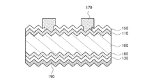
110 シリコン半導体層
110a n+型領域
110b n−型領域
130 酸化物半導体層
150 透光性薄膜
160 パッシベーション層
170 第1の電極
180 シリコン半導体層
190 第2の電極
220 第1の不純物領域
230 第2の不純物領域
240 不純物領域
260 絶縁層
270 第1の電極
290 第2の電極
Claims (5)
- 第1の電極と、
第2の電極と、
前記第1の電極及び前記第2の電極の間に設けられたシリコン基板と、
前記第1の電極及び前記シリコン基板の間に設けられた第1のシリコン層と、
前記第1の電極及び前記第1のシリコン層の間に設けられたパッシベーション層と、
前記第1の電極及び前記パッシベーション層の間に設けられた、透光性を有する薄膜と、
前記第2の電極及び前記シリコン基板の間に設けられ、前記シリコン基板と接する酸化物半導体層と、を有し、
前記酸化物半導体層は、前記シリコン基板の一方の面の略全面と接し、
前記第2の電極は、前記酸化物半導体層の一方の面の略全面と接し、
前記酸化物半導体層は、前記シリコン基板の表面欠陥を終端する機能を有し、
前記パッシベーション層は、前記第1のシリコン層の表面欠陥を低減する機能を有し、
前記第1のシリコン層は、前記シリコン基板と逆の導電型を有することを特徴とする光電変換装置。 - 請求項1において、
前記第1のシリコン層は、第1の領域と、前記第1の領域よりもキャリア濃度が高い第2の領域と、を有し、
前記第1の電極は、前記第2の領域と接する領域を有することを特徴とする光電変換装置。 - 請求項1または請求項2において、
前記酸化物半導体層は、バンドギャップが2eV以上であることを特徴とする光電変換装置。 - 請求項1または請求項2において、
前記酸化物半導体層は、元素周期表において第4族乃至第8族に属する金属を含むことを特徴とする光電変換装置。 - 請求項1または請求項2において、
前記酸化物半導体層は、酸化バナジウム、酸化ニオブ、酸化タンタル、酸化クロム、酸化モリブデン、酸化タングステン、酸化マンガン、または酸化レニウムを含むことを特徴とする光電変換装置。
Priority Applications (1)
| Application Number | Priority Date | Filing Date | Title |
|---|---|---|---|
| JP2013006813A JP6254348B2 (ja) | 2012-01-18 | 2013-01-18 | 光電変換装置 |
Applications Claiming Priority (5)
| Application Number | Priority Date | Filing Date | Title |
|---|---|---|---|
| JP2012007650 | 2012-01-18 | ||
| JP2012007650 | 2012-01-18 | ||
| JP2012107483 | 2012-05-09 | ||
| JP2012107483 | 2012-05-09 | ||
| JP2013006813A JP6254348B2 (ja) | 2012-01-18 | 2013-01-18 | 光電変換装置 |
Publications (3)
| Publication Number | Publication Date |
|---|---|
| JP2013254932A JP2013254932A (ja) | 2013-12-19 |
| JP2013254932A5 JP2013254932A5 (ja) | 2016-01-21 |
| JP6254348B2 true JP6254348B2 (ja) | 2017-12-27 |
Family
ID=48779133
Family Applications (1)
| Application Number | Title | Priority Date | Filing Date |
|---|---|---|---|
| JP2013006813A Expired - Fee Related JP6254348B2 (ja) | 2012-01-18 | 2013-01-18 | 光電変換装置 |
Country Status (3)
| Country | Link |
|---|---|
| US (1) | US20130180577A1 (ja) |
| JP (1) | JP6254348B2 (ja) |
| CN (1) | CN103219398B (ja) |
Families Citing this family (4)
| Publication number | Priority date | Publication date | Assignee | Title |
|---|---|---|---|---|
| TWI469380B (zh) * | 2013-11-08 | 2015-01-11 | Ind Tech Res Inst | 異質接面太陽電池結構 |
| JP6305105B2 (ja) * | 2014-02-27 | 2018-04-04 | 日立造船株式会社 | 太陽電池 |
| CN107425083A (zh) * | 2017-07-26 | 2017-12-01 | 顺德中山大学太阳能研究院 | 一种叠层背钝化太阳能电池及其制备方法 |
| CN109786503A (zh) * | 2018-12-29 | 2019-05-21 | 浙江师范大学 | 用氧化钼对单晶硅表面进行钝化的方法 |
Family Cites Families (17)
| Publication number | Priority date | Publication date | Assignee | Title |
|---|---|---|---|---|
| DE4217428A1 (de) * | 1991-12-09 | 1993-06-17 | Deutsche Aerospace | Hochleistungs-solarzellenstruktur |
| WO1998043304A1 (fr) * | 1997-03-21 | 1998-10-01 | Sanyo Electric Co., Ltd. | Element photovoltaique et procede de fabrication dudit element |
| US7382421B2 (en) * | 2004-10-12 | 2008-06-03 | Hewlett-Packard Development Company, L.P. | Thin film transistor with a passivation layer |
| US7375378B2 (en) * | 2005-05-12 | 2008-05-20 | General Electric Company | Surface passivated photovoltaic devices |
| JP4568254B2 (ja) * | 2006-07-20 | 2010-10-27 | 三洋電機株式会社 | 太陽電池モジュール |
| US7968792B2 (en) * | 2007-03-05 | 2011-06-28 | Seagate Technology Llc | Quantum dot sensitized wide bandgap semiconductor photovoltaic devices & methods of fabricating same |
| TW200841393A (en) * | 2007-04-02 | 2008-10-16 | Miin-Jang Chen | Optoelectronic device and method of fabricating the same |
| JP5277485B2 (ja) * | 2007-12-13 | 2013-08-28 | シャープ株式会社 | 太陽電池の製造方法 |
| KR20090091562A (ko) * | 2008-02-25 | 2009-08-28 | 엘지전자 주식회사 | 태양전지 및 그 제조방법 |
| JP5250412B2 (ja) * | 2008-12-26 | 2013-07-31 | Tdk株式会社 | 光電変換素子用色素および光電変換素子 |
| US8129216B2 (en) * | 2009-04-29 | 2012-03-06 | International Business Machines Corporation | Method of manufacturing solar cell with doping patterns and contacts |
| KR20120067361A (ko) * | 2009-09-18 | 2012-06-25 | 어플라이드 머티어리얼스, 인코포레이티드 | 태양 전지에서 표면 재결합을 감소시키기 위한 한계치 조절 주입 |
| JP2011146528A (ja) * | 2010-01-14 | 2011-07-28 | Kaneka Corp | 多結晶シリコン系太陽電池およびその製造方法 |
| US20120031484A1 (en) * | 2010-08-06 | 2012-02-09 | E. I. Du Pont De Nemours And Company | Conductive paste for a solar cell electrode |
| US20120111399A1 (en) * | 2010-11-08 | 2012-05-10 | E. I. Du Pont De Nemours And Company | Solar cell electrode |
| US20120255612A1 (en) * | 2011-04-08 | 2012-10-11 | Dieter Pierreux | Ald of metal oxide film using precursor pairs with different oxidants |
| CN102184985B (zh) * | 2011-04-30 | 2013-09-04 | 常州天合光能有限公司 | 一种太阳能电池浮动结背面钝化结构及其方法 |
-
2013
- 2013-01-02 US US13/732,604 patent/US20130180577A1/en not_active Abandoned
- 2013-01-17 CN CN201310017189.0A patent/CN103219398B/zh not_active Expired - Fee Related
- 2013-01-18 JP JP2013006813A patent/JP6254348B2/ja not_active Expired - Fee Related
Also Published As
| Publication number | Publication date |
|---|---|
| CN103219398B (zh) | 2017-09-12 |
| JP2013254932A (ja) | 2013-12-19 |
| US20130180577A1 (en) | 2013-07-18 |
| CN103219398A (zh) | 2013-07-24 |
Similar Documents
| Publication | Publication Date | Title |
|---|---|---|
| JP5844797B2 (ja) | 太陽電池の製造方法 | |
| JP6329660B2 (ja) | 光電変換装置 | |
| JP5570654B2 (ja) | 太陽電池素子および太陽電池モジュール | |
| JP6254343B2 (ja) | 光電変換装置 | |
| US8889464B2 (en) | Method for manufacturing solar cell | |
| US20120273036A1 (en) | Photoelectric conversion device and manufacturing method thereof | |
| US9761749B2 (en) | Photoelectric conversion device | |
| JP6254348B2 (ja) | 光電変換装置 | |
| JP5826094B2 (ja) | p型半導体材料、および光電変換装置の作製方法 | |
| JP2015138959A (ja) | 光起電力装置および光起電力装置の製造方法 | |
| US9437768B2 (en) | Photoelectric conversion device | |
| JP2017005270A (ja) | 光電変換装置の作製方法 | |
| JP6139731B2 (ja) | 光電変換装置の作製方法 | |
| US11631779B2 (en) | Solar cell with high photoelectric conversion efficiency and method for manufacturing solar cell with high photoelectric conversion efficiency | |
| JPWO2018179656A1 (ja) | 太陽電池、太陽電池モジュール、および、太陽電池の製造方法 | |
| TW201719914A (zh) | 光發電元件及其製造方法 | |
| TW201709541A (zh) | 光發電元件及其製造方法 | |
| JP2013125884A (ja) | 光電変換装置の作製方法および光電変換装置 | |
| KR102563642B1 (ko) | 고효율 이면전극형 태양전지 및 그 제조방법 | |
| JP7346050B2 (ja) | 太陽電池セルおよび太陽電池モジュール | |
| JP5316491B2 (ja) | 太陽電池の製造方法 | |
| Li et al. | Photovoltaic Performance Enhancement of Textured Silicon Solar Cells Using Luminescent Down-Shifting Methylammonium Lead Tribromide Perovskite Nanophosphors |
Legal Events
| Date | Code | Title | Description |
|---|---|---|---|
| A521 | Request for written amendment filed |
Free format text: JAPANESE INTERMEDIATE CODE: A523 Effective date: 20151125 |
|
| A621 | Written request for application examination |
Free format text: JAPANESE INTERMEDIATE CODE: A621 Effective date: 20151125 |
|
| A977 | Report on retrieval |
Free format text: JAPANESE INTERMEDIATE CODE: A971007 Effective date: 20160729 |
|
| A131 | Notification of reasons for refusal |
Free format text: JAPANESE INTERMEDIATE CODE: A131 Effective date: 20160802 |
|
| A521 | Request for written amendment filed |
Free format text: JAPANESE INTERMEDIATE CODE: A523 Effective date: 20160923 |
|
| A131 | Notification of reasons for refusal |
Free format text: JAPANESE INTERMEDIATE CODE: A131 Effective date: 20170307 |
|
| A521 | Request for written amendment filed |
Free format text: JAPANESE INTERMEDIATE CODE: A523 Effective date: 20170502 |
|
| TRDD | Decision of grant or rejection written | ||
| A01 | Written decision to grant a patent or to grant a registration (utility model) |
Free format text: JAPANESE INTERMEDIATE CODE: A01 Effective date: 20171107 |
|
| A61 | First payment of annual fees (during grant procedure) |
Free format text: JAPANESE INTERMEDIATE CODE: A61 Effective date: 20171130 |
|
| R150 | Certificate of patent or registration of utility model |
Ref document number: 6254348 Country of ref document: JP Free format text: JAPANESE INTERMEDIATE CODE: R150 |
|
| LAPS | Cancellation because of no payment of annual fees |