JP6234975B2 - 半導体装置 - Google Patents
半導体装置 Download PDFInfo
- Publication number
- JP6234975B2 JP6234975B2 JP2015196735A JP2015196735A JP6234975B2 JP 6234975 B2 JP6234975 B2 JP 6234975B2 JP 2015196735 A JP2015196735 A JP 2015196735A JP 2015196735 A JP2015196735 A JP 2015196735A JP 6234975 B2 JP6234975 B2 JP 6234975B2
- Authority
- JP
- Japan
- Prior art keywords
- layer
- threshold voltage
- voltage adjustment
- electron supply
- adjustment layer
- Prior art date
- Legal status (The legal status is an assumption and is not a legal conclusion. Google has not performed a legal analysis and makes no representation as to the accuracy of the status listed.)
- Active
Links
- 239000004065 semiconductor Substances 0.000 title claims description 32
- 239000013078 crystal Substances 0.000 claims description 13
- 150000004767 nitrides Chemical class 0.000 claims description 12
- 230000007547 defect Effects 0.000 claims description 10
- 229910052721 tungsten Inorganic materials 0.000 claims description 9
- 239000012535 impurity Substances 0.000 claims description 8
- 229910052751 metal Inorganic materials 0.000 claims description 4
- 239000002184 metal Substances 0.000 claims description 4
- 229910004298 SiO 2 Inorganic materials 0.000 claims description 3
- 238000004544 sputter deposition Methods 0.000 claims description 3
- 238000000034 method Methods 0.000 description 24
- 239000000969 carrier Substances 0.000 description 12
- 230000005533 two-dimensional electron gas Effects 0.000 description 10
- WFKWXMTUELFFGS-UHFFFAOYSA-N tungsten Chemical compound [W] WFKWXMTUELFFGS-UHFFFAOYSA-N 0.000 description 5
- 239000010937 tungsten Substances 0.000 description 5
- 229910002704 AlGaN Inorganic materials 0.000 description 4
- 238000005516 engineering process Methods 0.000 description 4
- 238000004519 manufacturing process Methods 0.000 description 4
- 238000005530 etching Methods 0.000 description 3
- 230000005669 field effect Effects 0.000 description 3
- 239000000758 substrate Substances 0.000 description 3
- 229910052782 aluminium Inorganic materials 0.000 description 2
- 239000007789 gas Substances 0.000 description 2
- WQJQOUPTWCFRMM-UHFFFAOYSA-N tungsten disilicide Chemical compound [Si]#[W]#[Si] WQJQOUPTWCFRMM-UHFFFAOYSA-N 0.000 description 2
- 229910021342 tungsten silicide Inorganic materials 0.000 description 2
- XAGFODPZIPBFFR-UHFFFAOYSA-N aluminium Chemical compound [Al] XAGFODPZIPBFFR-UHFFFAOYSA-N 0.000 description 1
- 238000013459 approach Methods 0.000 description 1
- 230000004888 barrier function Effects 0.000 description 1
- 239000003990 capacitor Substances 0.000 description 1
- 238000009792 diffusion process Methods 0.000 description 1
- 230000000694 effects Effects 0.000 description 1
- 229910052733 gallium Inorganic materials 0.000 description 1
- 229910052738 indium Inorganic materials 0.000 description 1
- 238000009413 insulation Methods 0.000 description 1
- 239000000463 material Substances 0.000 description 1
- 238000012986 modification Methods 0.000 description 1
- 230000004048 modification Effects 0.000 description 1
Images

Classifications
-
- H—ELECTRICITY
- H01—ELECTRIC ELEMENTS
- H01L—SEMICONDUCTOR DEVICES NOT COVERED BY CLASS H10
- H01L29/00—Semiconductor devices specially adapted for rectifying, amplifying, oscillating or switching and having potential barriers; Capacitors or resistors having potential barriers, e.g. a PN-junction depletion layer or carrier concentration layer; Details of semiconductor bodies or of electrodes thereof ; Multistep manufacturing processes therefor
- H01L29/66—Types of semiconductor device ; Multistep manufacturing processes therefor
- H01L29/68—Types of semiconductor device ; Multistep manufacturing processes therefor controllable by only the electric current supplied, or only the electric potential applied, to an electrode which does not carry the current to be rectified, amplified or switched
- H01L29/76—Unipolar devices, e.g. field effect transistors
- H01L29/772—Field effect transistors
- H01L29/778—Field effect transistors with two-dimensional charge carrier gas channel, e.g. HEMT ; with two-dimensional charge-carrier layer formed at a heterojunction interface
- H01L29/7786—Field effect transistors with two-dimensional charge carrier gas channel, e.g. HEMT ; with two-dimensional charge-carrier layer formed at a heterojunction interface with direct single heterostructure, i.e. with wide bandgap layer formed on top of active layer, e.g. direct single heterostructure MIS-like HEMT
- H01L29/7787—Field effect transistors with two-dimensional charge carrier gas channel, e.g. HEMT ; with two-dimensional charge-carrier layer formed at a heterojunction interface with direct single heterostructure, i.e. with wide bandgap layer formed on top of active layer, e.g. direct single heterostructure MIS-like HEMT with wide bandgap charge-carrier supplying layer, e.g. direct single heterostructure MODFET
-
- H—ELECTRICITY
- H01—ELECTRIC ELEMENTS
- H01L—SEMICONDUCTOR DEVICES NOT COVERED BY CLASS H10
- H01L29/00—Semiconductor devices specially adapted for rectifying, amplifying, oscillating or switching and having potential barriers; Capacitors or resistors having potential barriers, e.g. a PN-junction depletion layer or carrier concentration layer; Details of semiconductor bodies or of electrodes thereof ; Multistep manufacturing processes therefor
- H01L29/40—Electrodes ; Multistep manufacturing processes therefor
- H01L29/43—Electrodes ; Multistep manufacturing processes therefor characterised by the materials of which they are formed
- H01L29/432—Heterojunction gate for field effect devices
-
- H—ELECTRICITY
- H01—ELECTRIC ELEMENTS
- H01L—SEMICONDUCTOR DEVICES NOT COVERED BY CLASS H10
- H01L29/00—Semiconductor devices specially adapted for rectifying, amplifying, oscillating or switching and having potential barriers; Capacitors or resistors having potential barriers, e.g. a PN-junction depletion layer or carrier concentration layer; Details of semiconductor bodies or of electrodes thereof ; Multistep manufacturing processes therefor
- H01L29/02—Semiconductor bodies ; Multistep manufacturing processes therefor
- H01L29/06—Semiconductor bodies ; Multistep manufacturing processes therefor characterised by their shape; characterised by the shapes, relative sizes, or dispositions of the semiconductor regions ; characterised by the concentration or distribution of impurities within semiconductor regions
- H01L29/10—Semiconductor bodies ; Multistep manufacturing processes therefor characterised by their shape; characterised by the shapes, relative sizes, or dispositions of the semiconductor regions ; characterised by the concentration or distribution of impurities within semiconductor regions with semiconductor regions connected to an electrode not carrying current to be rectified, amplified or switched and such electrode being part of a semiconductor device which comprises three or more electrodes
- H01L29/1066—Gate region of field-effect devices with PN junction gate
-
- H—ELECTRICITY
- H01—ELECTRIC ELEMENTS
- H01L—SEMICONDUCTOR DEVICES NOT COVERED BY CLASS H10
- H01L29/00—Semiconductor devices specially adapted for rectifying, amplifying, oscillating or switching and having potential barriers; Capacitors or resistors having potential barriers, e.g. a PN-junction depletion layer or carrier concentration layer; Details of semiconductor bodies or of electrodes thereof ; Multistep manufacturing processes therefor
- H01L29/02—Semiconductor bodies ; Multistep manufacturing processes therefor
- H01L29/12—Semiconductor bodies ; Multistep manufacturing processes therefor characterised by the materials of which they are formed
- H01L29/20—Semiconductor bodies ; Multistep manufacturing processes therefor characterised by the materials of which they are formed including, apart from doping materials or other impurities, only AIIIBV compounds
- H01L29/201—Semiconductor bodies ; Multistep manufacturing processes therefor characterised by the materials of which they are formed including, apart from doping materials or other impurities, only AIIIBV compounds including two or more compounds, e.g. alloys
- H01L29/205—Semiconductor bodies ; Multistep manufacturing processes therefor characterised by the materials of which they are formed including, apart from doping materials or other impurities, only AIIIBV compounds including two or more compounds, e.g. alloys in different semiconductor regions, e.g. heterojunctions
-
- H—ELECTRICITY
- H01—ELECTRIC ELEMENTS
- H01L—SEMICONDUCTOR DEVICES NOT COVERED BY CLASS H10
- H01L29/00—Semiconductor devices specially adapted for rectifying, amplifying, oscillating or switching and having potential barriers; Capacitors or resistors having potential barriers, e.g. a PN-junction depletion layer or carrier concentration layer; Details of semiconductor bodies or of electrodes thereof ; Multistep manufacturing processes therefor
- H01L29/66—Types of semiconductor device ; Multistep manufacturing processes therefor
- H01L29/68—Types of semiconductor device ; Multistep manufacturing processes therefor controllable by only the electric current supplied, or only the electric potential applied, to an electrode which does not carry the current to be rectified, amplified or switched
- H01L29/76—Unipolar devices, e.g. field effect transistors
- H01L29/772—Field effect transistors
- H01L29/778—Field effect transistors with two-dimensional charge carrier gas channel, e.g. HEMT ; with two-dimensional charge-carrier layer formed at a heterojunction interface
- H01L29/7786—Field effect transistors with two-dimensional charge carrier gas channel, e.g. HEMT ; with two-dimensional charge-carrier layer formed at a heterojunction interface with direct single heterostructure, i.e. with wide bandgap layer formed on top of active layer, e.g. direct single heterostructure MIS-like HEMT
-
- H—ELECTRICITY
- H01—ELECTRIC ELEMENTS
- H01L—SEMICONDUCTOR DEVICES NOT COVERED BY CLASS H10
- H01L29/00—Semiconductor devices specially adapted for rectifying, amplifying, oscillating or switching and having potential barriers; Capacitors or resistors having potential barriers, e.g. a PN-junction depletion layer or carrier concentration layer; Details of semiconductor bodies or of electrodes thereof ; Multistep manufacturing processes therefor
- H01L29/02—Semiconductor bodies ; Multistep manufacturing processes therefor
- H01L29/12—Semiconductor bodies ; Multistep manufacturing processes therefor characterised by the materials of which they are formed
- H01L29/20—Semiconductor bodies ; Multistep manufacturing processes therefor characterised by the materials of which they are formed including, apart from doping materials or other impurities, only AIIIBV compounds
- H01L29/2003—Nitride compounds
-
- H—ELECTRICITY
- H01—ELECTRIC ELEMENTS
- H01L—SEMICONDUCTOR DEVICES NOT COVERED BY CLASS H10
- H01L29/00—Semiconductor devices specially adapted for rectifying, amplifying, oscillating or switching and having potential barriers; Capacitors or resistors having potential barriers, e.g. a PN-junction depletion layer or carrier concentration layer; Details of semiconductor bodies or of electrodes thereof ; Multistep manufacturing processes therefor
- H01L29/02—Semiconductor bodies ; Multistep manufacturing processes therefor
- H01L29/12—Semiconductor bodies ; Multistep manufacturing processes therefor characterised by the materials of which they are formed
- H01L29/20—Semiconductor bodies ; Multistep manufacturing processes therefor characterised by the materials of which they are formed including, apart from doping materials or other impurities, only AIIIBV compounds
- H01L29/201—Semiconductor bodies ; Multistep manufacturing processes therefor characterised by the materials of which they are formed including, apart from doping materials or other impurities, only AIIIBV compounds including two or more compounds, e.g. alloys
-
- H—ELECTRICITY
- H01—ELECTRIC ELEMENTS
- H01L—SEMICONDUCTOR DEVICES NOT COVERED BY CLASS H10
- H01L29/00—Semiconductor devices specially adapted for rectifying, amplifying, oscillating or switching and having potential barriers; Capacitors or resistors having potential barriers, e.g. a PN-junction depletion layer or carrier concentration layer; Details of semiconductor bodies or of electrodes thereof ; Multistep manufacturing processes therefor
- H01L29/02—Semiconductor bodies ; Multistep manufacturing processes therefor
- H01L29/30—Semiconductor bodies ; Multistep manufacturing processes therefor characterised by physical imperfections; having polished or roughened surface
- H01L29/34—Semiconductor bodies ; Multistep manufacturing processes therefor characterised by physical imperfections; having polished or roughened surface the imperfections being on the surface
-
- H—ELECTRICITY
- H01—ELECTRIC ELEMENTS
- H01L—SEMICONDUCTOR DEVICES NOT COVERED BY CLASS H10
- H01L29/00—Semiconductor devices specially adapted for rectifying, amplifying, oscillating or switching and having potential barriers; Capacitors or resistors having potential barriers, e.g. a PN-junction depletion layer or carrier concentration layer; Details of semiconductor bodies or of electrodes thereof ; Multistep manufacturing processes therefor
- H01L29/40—Electrodes ; Multistep manufacturing processes therefor
- H01L29/43—Electrodes ; Multistep manufacturing processes therefor characterised by the materials of which they are formed
- H01L29/47—Schottky barrier electrodes
- H01L29/475—Schottky barrier electrodes on AIII-BV compounds
Landscapes
- Engineering & Computer Science (AREA)
- Microelectronics & Electronic Packaging (AREA)
- Power Engineering (AREA)
- Physics & Mathematics (AREA)
- Ceramic Engineering (AREA)
- Condensed Matter Physics & Semiconductors (AREA)
- General Physics & Mathematics (AREA)
- Computer Hardware Design (AREA)
- Junction Field-Effect Transistors (AREA)
- Insulated Gate Type Field-Effect Transistor (AREA)
Description
特許文献6〜7の技術は、オン抵抗の増加を防止することを意図した技術であるが、結果的にはゲート電極からのリーク電流を低く抑える効果を持つ。しかしながら、この技術によっても、閾値電圧が、場合によってまたは経時的に変化する現象を抑制できないことが判明した。
本明細書では、ゲート電極からのリーク電流が低く抑えられ、閾値電圧の変化が抑制されている半導体装置を開示する。
特許文献6〜7の技術では、閾値電圧調整層から電子供給層にキャリアが移動して閾値電圧調整層の帯電電荷量が変化することを防止できる。しかしながら、ゲート電極から閾値電圧調整層にキャリアが移動することには対策しておらず、閾値電圧調整層の帯電電荷量が一定に維持されない。特許文献6〜7の技術でも、閾値電圧調整層の帯電電荷量が、場合によってあるいは経時的に変化し、それによって閾値電圧が変化してしまう。
電子走行層はGaNで形成されている。電子供給層は、Inx1Aly1Ga1−x1−y1N(0≦x1<1,0≦y1<1,0<1−x1−y1<1)で形成されており、電子走行層上に形成されている。ソース電極とドレイン電極は、電子供給層上に形成されている。ソース電極とドレイン電極は、相互に離れた位置に形成されている。閾値電圧調整層は、p型のInx2Aly2Ga1−x2−y2N(0≦x2<1,0≦y2<1,0<1−x2−y2≦1)で形成されており、電子供給層上に形成されている。閾値電圧調整層は、ソース電極とドレイン電極の間の一部に位置している。ゲート電極は、閾値電圧調整層上に形成されている。
(1)閾値電圧調整層の上にタングステン(W)またはWを含む金属をスパッタリングする。すると、閾値電圧調整層に結晶欠陥層が形成され、それが高抵抗層となる。その手法によって形成した半導体装置は、ゲート電極がタングステン(W)を含んでおり、ゲート電極と閾値電圧調整層の界面に、閾値電圧調整層上にWまたはWを含む金属をスパッタリングした際に生じた結晶欠陥層が露出している。
閾値電圧調整層がp型のGaNで形成されている場合は、ゲート電極と閾値電圧調整層の間に、
(2)不純物を低濃度に含む(従って高抵抗な)p型GaNを介在させる、
(3)i型のGaN(意図的な不純物添加をしていないGaN)を介在させる、
(4)n型GaNを介在させる、
(5)いわゆる絶縁層(SiO2,SiN,AlO,GaOなど)を介在させる、または
(6)閾値電圧調整層との間にヘテロ接合を形成する窒化物半導体層が介在させるといった手法を用いることができる。
ここでいう高抵抗層は、閾値電圧調整層よりも高抵抗な層をいう。また層といっても厚みを有するものに限られず、pn接合あるいはヘテロ接合に形成される障壁がキャリアの移動を阻止するものを含む。高抵抗層に、いわゆる絶縁層を用いることが好ましい。絶縁層は抵抗が著しく高く、閾値電圧の変動抑制に最も効果的である。
電子供給層がアルミニウム(Al)を含んでいる場合、そのAl組成比を、閾値電圧調整層側で高くして電子走行層側で低くする。Al組成比が高い領域が高抵抗層となる。
ここでいう高抵抗層とは、閾値電圧調整層と電子供給層の双方よりも高抵抗なことをいう。前記の場合、高抵抗層が電子供給層の一部であるといえる。この場合、閾値電圧調整層に接する範囲の電子供給層の抵抗が、それ以外の範囲の電子供給層の抵抗より高抵抗であるので、閾値電圧調整層と電子供給層の間に高抵抗層が介在しているということができる。
(特徴1)ゲート電極はタングステンで形成されている。ゲート電極を構成するタンクステンと閾値電圧調整層を構成する窒化物半導体の間にはショットキー容量(C2)が存在する。また閾値電圧調整層を構成する窒化物半導体と電子供給層を構成する窒化物半導体の間にも容量(C1)が存在する。容量C2と容量C1の合成容量によって、閾値電圧を制御することができる。
(特徴2)ゲート電極はタングステンシリサイドで形成されている。Si半導体の製造ラインではゲート電極形成用にタングステンシリサイドが多用される。その多用技術を流用することができる。
(特徴3)電子供給層がAlGaNで形成され、閾値電圧調整層がGaNで形成されている。
(特徴4)電子供給層のAl組成が深さともに連続的または断続的に変化している。
(特徴5)閾値電圧調整層に接する範囲では、電子供給層のAl組成が、AlとInとGaの総量に対して25%以上である。
(特徴6)電子供給層はInを含み、閾値電圧調整層はInを含まない。
(特徴7)電子供給層はInを含まず、閾値電圧調整層はInを含む。
(特徴8)p型のInx2Aly2Ga1−x2−y2Nで形成されている閾値電圧調整層には結晶欠陥が存在し、その結晶欠陥にキャリアをトラップしている。
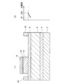
図1は、第1実施例の半導体装置(2次元電子ガスを利用する電界効果トランジスタ)の断面図であり、基板2上にバッファ層4が結晶成長し、バッファ層4上にi型のGaN層6が結晶成長し、i型のGaN層6上にi型のAly1Ga1−y1N層8(0<y1<1)が結晶成長している。本明細書では、p型またはn型にするための不純物を添加する処理をしないで結晶成長した場合をi型という。本実施例では、y1=0.25であり、その膜圧は30nmである。Alを含まないGaN層6上にAlを含むGaN層8が結晶成長しているヘテロ接合では、前者のバンドギャップよりも後者のバンドギャップが広いことから、GaN層6のヘテロ接合界面に面した領域に2次元電子ガスが生成される。本明細書では、2次元電子ガスが生成されるGaN層6を電子走行層といい、2次元電子ガスを生成するAlGaN層8を電子供給層という。電子供給層8の表面上にソース電極18とドレイン電極20が形成されている。ソース電極18とドレイン電極20は、相互に離れた位置に形成されている。ソース電極18とヘテロ接合界面の間に介在する範囲の電子供給層8と、ドレイン電極20とヘテロ接合界面の間に介在する範囲の電子供給層8は、例えば電極18,20を形成する金属が拡散するなどして低抵抗となっている。電子走行層6がi型であることから、電子の移動度が高く、ソース電極18とドレイン電極20の間が低抵抗となる。
第2実施例の半導体装置では、図2に示すように、電子供給層8とは別の結晶構造を持つ高抵抗層10が存在しない。ただし、電子供給層8を形成するAly1Ga1-y1N(0≦y1<1,0<1−y1<1)のAl組成(y1の値)が、深さ方向に変化(傾斜)している。すなわち、閾値電圧調整層12に接する上面では、y1=0.25であり、電子走行層6に接する下面では、y1=0.05であり、その間の深さでは連続的に変化している。この場合、Al組成(y1の値)が高いほど絶縁性が高く、高抵抗である。閾値電圧調整層12に接するy1=0.25の範囲は、残部よりも高抵抗であり、高抵抗層となっているということができる。元素の組成比を変えることで高抵抗層を製造する技術によると、原料ガスの配合比を変えながら結晶成長を続けることができる。製造時間を短時間化することができる。これに対して、組成自体を異にする高抵抗層を製膜するためには、材料ガスの供給を停止して置換する処理が必要となり、製造時間が長時間化する。
第2実施例の電界効果トランジスタでも、リーク電流が低く、閾値電圧が常に安定している。閾値電圧が、場合によってあるいは経時的に変化するのを抑制する。
4:バッファ層
6:電子走行層
8:電子供給層
10:高抵抗層
12:閾値電圧調整層
14:高抵抗層
16:ゲート電極
18:ソース電極
20:ドレイン電極
Claims (4)
- GaNで形成されている電子走行層と、
前記電子走行層上に形成されており、Inx1Aly1Ga1-x1-y1N(0≦x1<1,0<y1<1,0<1−x1−y1<1)で形成されている電子供給層と、
前記電子供給層上の相互に離れた位置に形成されているソース電極とドレイン電極と、
前記ソース電極と前記ドレイン電極の間に位置する前記電子供給層上の一部に形成されており、p型のInx2Aly2Ga1-x2-y2N(0≦x2<1,0≦y2<1,0<1−x2−y2≦1)で形成されている閾値電圧調整層と、
前記閾値電圧調整層上に形成されているゲート電極を備えており、
前記ゲート電極と前記閾値電圧調整層の間と、前記閾値電圧調整層と前記電子供給層の間の双方に、高抵抗層が介在しており、
前記電子供給層がAlを含み、そのAl組成比が前記閾値電圧調整層の側で高くて前記電子走行層の側で低く、
前記Al組成比の高い層が、前記閾値電圧調整層と前記電子供給層の間の前記高抵抗層となっている半導体装置。 - 前記ゲート電極がWを含み、
前記ゲート電極と前記閾値電圧調整層の界面に、前記閾値電圧調整層上にWまたはWを含む金属をスパッタリングした際に生じた結晶欠陥層が露出しており、その結晶欠陥層が前記ゲート電極と前記閾値電圧調整層の間の前記高抵抗層となっている請求項1に記載の半導体装置。 - 前記閾値電圧調整層がp型のGaNで形成されており、
前記ゲート電極と前記閾値電圧調整層の間に、不純物を低濃度に含むp型GaN,i型のGaN,n型GaN、絶縁層(SiO2,SiN,AlO,GaO)、または、前記閾値電圧調整層との間にヘテロ接合を形成する窒化物半導体層が介在している請求項1に記載の半導体装置。 - 前記電子供給層と前記閾値電圧調整層のうちの一方がInを含み、他方がInを含まない請求項1から3のいずれかの一項に記載の半導体装置。
Priority Applications (2)
| Application Number | Priority Date | Filing Date | Title |
|---|---|---|---|
| JP2015196735A JP6234975B2 (ja) | 2015-10-02 | 2015-10-02 | 半導体装置 |
| US15/240,745 US9773900B2 (en) | 2015-10-02 | 2016-08-18 | Semiconductor device |
Applications Claiming Priority (1)
| Application Number | Priority Date | Filing Date | Title |
|---|---|---|---|
| JP2015196735A JP6234975B2 (ja) | 2015-10-02 | 2015-10-02 | 半導体装置 |
Publications (2)
| Publication Number | Publication Date |
|---|---|
| JP2017069515A JP2017069515A (ja) | 2017-04-06 |
| JP6234975B2 true JP6234975B2 (ja) | 2017-11-22 |
Family
ID=58447644
Family Applications (1)
| Application Number | Title | Priority Date | Filing Date |
|---|---|---|---|
| JP2015196735A Active JP6234975B2 (ja) | 2015-10-02 | 2015-10-02 | 半導体装置 |
Country Status (2)
| Country | Link |
|---|---|
| US (1) | US9773900B2 (ja) |
| JP (1) | JP6234975B2 (ja) |
Families Citing this family (3)
| Publication number | Priority date | Publication date | Assignee | Title |
|---|---|---|---|---|
| CN110021661B (zh) * | 2019-04-26 | 2022-06-17 | 江苏能华微电子科技发展有限公司 | 半导体器件及其制作方法 |
| CN112368842B (zh) * | 2020-09-09 | 2022-12-06 | 英诺赛科(苏州)科技有限公司 | 半导体装置结构和其制造方法 |
| CN114256343A (zh) * | 2020-09-24 | 2022-03-29 | 联华电子股份有限公司 | 高电子迁移率晶体管及其制作方法 |
Family Cites Families (16)
| Publication number | Priority date | Publication date | Assignee | Title |
|---|---|---|---|---|
| KR100571071B1 (ko) * | 1996-12-04 | 2006-06-21 | 소니 가부시끼 가이샤 | 전계효과트랜지스터및그제조방법 |
| US7612390B2 (en) * | 2004-02-05 | 2009-11-03 | Cree, Inc. | Heterojunction transistors including energy barriers |
| JP5486166B2 (ja) * | 2008-06-16 | 2014-05-07 | 株式会社豊田中央研究所 | 半導体装置とその製造方法 |
| JP2011029507A (ja) | 2009-07-28 | 2011-02-10 | Panasonic Corp | 半導体装置 |
| US8895993B2 (en) * | 2011-01-31 | 2014-11-25 | Taiwan Semiconductor Manufacturing Company, Ltd. | Low gate-leakage structure and method for gallium nitride enhancement mode transistor |
| US8604486B2 (en) | 2011-06-10 | 2013-12-10 | International Rectifier Corporation | Enhancement mode group III-V high electron mobility transistor (HEMT) and method for fabrication |
| JP2013074179A (ja) * | 2011-09-28 | 2013-04-22 | Fujitsu Ltd | 化合物半導体装置及びその製造方法 |
| KR101882997B1 (ko) | 2011-09-30 | 2018-07-30 | 삼성전기주식회사 | 질화물 반도체 소자 및 그 제조방법 |
| JP2013207107A (ja) | 2012-03-28 | 2013-10-07 | Fujitsu Ltd | 化合物半導体装置及びその製造方法 |
| US9111905B2 (en) * | 2012-03-29 | 2015-08-18 | Taiwan Semiconductor Manufacturing Company, Ltd. | High electron mobility transistor and method of forming the same |
| JP2014027187A (ja) * | 2012-07-27 | 2014-02-06 | Fujitsu Ltd | 化合物半導体装置及びその製造方法 |
| US9837521B2 (en) * | 2012-10-11 | 2017-12-05 | Rohm Co., Ltd. | Nitride semiconductor device and fabrication method therefor |
| JP2014110393A (ja) | 2012-12-04 | 2014-06-12 | Fujitsu Ltd | 化合物半導体装置及びその製造方法 |
| JP2014207379A (ja) * | 2013-04-15 | 2014-10-30 | トランスフォーム・ジャパン株式会社 | 化合物半導体装置及びその製造方法 |
| JP5707463B2 (ja) * | 2013-09-30 | 2015-04-30 | 株式会社豊田中央研究所 | 半導体装置とその製造方法 |
| JP6170007B2 (ja) | 2014-04-10 | 2017-07-26 | トヨタ自動車株式会社 | スイッチング素子 |
-
2015
- 2015-10-02 JP JP2015196735A patent/JP6234975B2/ja active Active
-
2016
- 2016-08-18 US US15/240,745 patent/US9773900B2/en active Active
Also Published As
| Publication number | Publication date |
|---|---|
| JP2017069515A (ja) | 2017-04-06 |
| US9773900B2 (en) | 2017-09-26 |
| US20170098701A1 (en) | 2017-04-06 |
Similar Documents
| Publication | Publication Date | Title |
|---|---|---|
| JP6174874B2 (ja) | 半導体装置 | |
| JP6270572B2 (ja) | 半導体装置及びその製造方法 | |
| US20190140088A1 (en) | Nitride power transistor and manufacturing method thereof | |
| JP6189235B2 (ja) | 半導体装置 | |
| US20140110759A1 (en) | Semiconductor device | |
| US20150270379A1 (en) | Semiconductor device | |
| US20130240899A1 (en) | Nitride semiconductor device | |
| JP2013235873A (ja) | 半導体装置およびその製造方法 | |
| US8816399B2 (en) | Semiconductor device | |
| JP5919703B2 (ja) | 半導体装置 | |
| JP6330148B2 (ja) | 半導体装置 | |
| WO2015004853A1 (ja) | 半導体装置 | |
| JP2019525499A (ja) | 半導体デバイス及び半導体デバイスを設計する方法 | |
| JP5707463B2 (ja) | 半導体装置とその製造方法 | |
| TW201541635A (zh) | 半導體基板及半導體元件 | |
| US20150263155A1 (en) | Semiconductor device | |
| US20160211357A1 (en) | Semiconductor device | |
| JP6234975B2 (ja) | 半導体装置 | |
| TW201709514A (zh) | 增強型高電子遷移率電晶體結構 | |
| US20240105812A1 (en) | Nitride-based semiconductor device and method for manufacturing the same | |
| JP5793101B2 (ja) | 半導体装置 | |
| JP4801325B2 (ja) | Iii−v族窒化物半導体を用いた半導体装置 | |
| JP2007250727A (ja) | 電界効果トランジスタ | |
| US20160211358A1 (en) | Semiconductor device | |
| US9627489B2 (en) | Semiconductor device |
Legal Events
| Date | Code | Title | Description |
|---|---|---|---|
| A977 | Report on retrieval |
Free format text: JAPANESE INTERMEDIATE CODE: A971007 Effective date: 20170720 |
|
| A131 | Notification of reasons for refusal |
Free format text: JAPANESE INTERMEDIATE CODE: A131 Effective date: 20170725 |
|
| A521 | Request for written amendment filed |
Free format text: JAPANESE INTERMEDIATE CODE: A523 Effective date: 20170921 |
|
| TRDD | Decision of grant or rejection written | ||
| A01 | Written decision to grant a patent or to grant a registration (utility model) |
Free format text: JAPANESE INTERMEDIATE CODE: A01 Effective date: 20171017 |
|
| A61 | First payment of annual fees (during grant procedure) |
Free format text: JAPANESE INTERMEDIATE CODE: A61 Effective date: 20171025 |
|
| R150 | Certificate of patent or registration of utility model |
Ref document number: 6234975 Country of ref document: JP Free format text: JAPANESE INTERMEDIATE CODE: R150 |
|
| S111 | Request for change of ownership or part of ownership |
Free format text: JAPANESE INTERMEDIATE CODE: R313117 |
|
| R350 | Written notification of registration of transfer |
Free format text: JAPANESE INTERMEDIATE CODE: R350 |
|
| R250 | Receipt of annual fees |
Free format text: JAPANESE INTERMEDIATE CODE: R250 |
|
| R250 | Receipt of annual fees |
Free format text: JAPANESE INTERMEDIATE CODE: R250 |
|
| R250 | Receipt of annual fees |
Free format text: JAPANESE INTERMEDIATE CODE: R250 |