JP6220142B2 - 発光素子パッケージ - Google Patents
発光素子パッケージ Download PDFInfo
- Publication number
- JP6220142B2 JP6220142B2 JP2013078227A JP2013078227A JP6220142B2 JP 6220142 B2 JP6220142 B2 JP 6220142B2 JP 2013078227 A JP2013078227 A JP 2013078227A JP 2013078227 A JP2013078227 A JP 2013078227A JP 6220142 B2 JP6220142 B2 JP 6220142B2
- Authority
- JP
- Japan
- Prior art keywords
- light emitting
- surface portion
- light
- lead frame
- light source
- Prior art date
- Legal status (The legal status is an assumption and is not a legal conclusion. Google has not performed a legal analysis and makes no representation as to the accuracy of the status listed.)
- Active
Links
Images


Classifications
-
- H—ELECTRICITY
- H01—ELECTRIC ELEMENTS
- H01L—SEMICONDUCTOR DEVICES NOT COVERED BY CLASS H10
- H01L33/00—Semiconductor devices with at least one potential-jump barrier or surface barrier specially adapted for light emission; Processes or apparatus specially adapted for the manufacture or treatment thereof or of parts thereof; Details thereof
- H01L33/02—Semiconductor devices with at least one potential-jump barrier or surface barrier specially adapted for light emission; Processes or apparatus specially adapted for the manufacture or treatment thereof or of parts thereof; Details thereof characterised by the semiconductor bodies
- H01L33/08—Semiconductor devices with at least one potential-jump barrier or surface barrier specially adapted for light emission; Processes or apparatus specially adapted for the manufacture or treatment thereof or of parts thereof; Details thereof characterised by the semiconductor bodies with a plurality of light emitting regions, e.g. laterally discontinuous light emitting layer or photoluminescent region integrated within the semiconductor body
-
- F—MECHANICAL ENGINEERING; LIGHTING; HEATING; WEAPONS; BLASTING
- F21—LIGHTING
- F21S—NON-PORTABLE LIGHTING DEVICES; SYSTEMS THEREOF; VEHICLE LIGHTING DEVICES SPECIALLY ADAPTED FOR VEHICLE EXTERIORS
- F21S43/00—Signalling devices specially adapted for vehicle exteriors, e.g. brake lamps, direction indicator lights or reversing lights
- F21S43/10—Signalling devices specially adapted for vehicle exteriors, e.g. brake lamps, direction indicator lights or reversing lights characterised by the light source
- F21S43/13—Signalling devices specially adapted for vehicle exteriors, e.g. brake lamps, direction indicator lights or reversing lights characterised by the light source characterised by the type of light source
- F21S43/14—Light emitting diodes [LED]
-
- F—MECHANICAL ENGINEERING; LIGHTING; HEATING; WEAPONS; BLASTING
- F21—LIGHTING
- F21S—NON-PORTABLE LIGHTING DEVICES; SYSTEMS THEREOF; VEHICLE LIGHTING DEVICES SPECIALLY ADAPTED FOR VEHICLE EXTERIORS
- F21S43/00—Signalling devices specially adapted for vehicle exteriors, e.g. brake lamps, direction indicator lights or reversing lights
- F21S43/10—Signalling devices specially adapted for vehicle exteriors, e.g. brake lamps, direction indicator lights or reversing lights characterised by the light source
- F21S43/13—Signalling devices specially adapted for vehicle exteriors, e.g. brake lamps, direction indicator lights or reversing lights characterised by the light source characterised by the type of light source
- F21S43/15—Strips of light sources
-
- F—MECHANICAL ENGINEERING; LIGHTING; HEATING; WEAPONS; BLASTING
- F21—LIGHTING
- F21S—NON-PORTABLE LIGHTING DEVICES; SYSTEMS THEREOF; VEHICLE LIGHTING DEVICES SPECIALLY ADAPTED FOR VEHICLE EXTERIORS
- F21S43/00—Signalling devices specially adapted for vehicle exteriors, e.g. brake lamps, direction indicator lights or reversing lights
- F21S43/10—Signalling devices specially adapted for vehicle exteriors, e.g. brake lamps, direction indicator lights or reversing lights characterised by the light source
- F21S43/19—Attachment of light sources or lamp holders
- F21S43/195—Details of lamp holders, terminals or connectors
-
- F—MECHANICAL ENGINEERING; LIGHTING; HEATING; WEAPONS; BLASTING
- F21—LIGHTING
- F21S—NON-PORTABLE LIGHTING DEVICES; SYSTEMS THEREOF; VEHICLE LIGHTING DEVICES SPECIALLY ADAPTED FOR VEHICLE EXTERIORS
- F21S43/00—Signalling devices specially adapted for vehicle exteriors, e.g. brake lamps, direction indicator lights or reversing lights
- F21S43/20—Signalling devices specially adapted for vehicle exteriors, e.g. brake lamps, direction indicator lights or reversing lights characterised by refractors, transparent cover plates, light guides or filters
- F21S43/235—Light guides
- F21S43/236—Light guides characterised by the shape of the light guide
- F21S43/237—Light guides characterised by the shape of the light guide rod-shaped
-
- F—MECHANICAL ENGINEERING; LIGHTING; HEATING; WEAPONS; BLASTING
- F21—LIGHTING
- F21S—NON-PORTABLE LIGHTING DEVICES; SYSTEMS THEREOF; VEHICLE LIGHTING DEVICES SPECIALLY ADAPTED FOR VEHICLE EXTERIORS
- F21S43/00—Signalling devices specially adapted for vehicle exteriors, e.g. brake lamps, direction indicator lights or reversing lights
- F21S43/20—Signalling devices specially adapted for vehicle exteriors, e.g. brake lamps, direction indicator lights or reversing lights characterised by refractors, transparent cover plates, light guides or filters
- F21S43/235—Light guides
- F21S43/242—Light guides characterised by the emission area
- F21S43/245—Light guides characterised by the emission area emitting light from one or more of its major surfaces
-
- F—MECHANICAL ENGINEERING; LIGHTING; HEATING; WEAPONS; BLASTING
- F21—LIGHTING
- F21S—NON-PORTABLE LIGHTING DEVICES; SYSTEMS THEREOF; VEHICLE LIGHTING DEVICES SPECIALLY ADAPTED FOR VEHICLE EXTERIORS
- F21S43/00—Signalling devices specially adapted for vehicle exteriors, e.g. brake lamps, direction indicator lights or reversing lights
- F21S43/20—Signalling devices specially adapted for vehicle exteriors, e.g. brake lamps, direction indicator lights or reversing lights characterised by refractors, transparent cover plates, light guides or filters
- F21S43/235—Light guides
- F21S43/249—Light guides with two or more light sources being coupled into the light guide
-
- G—PHYSICS
- G02—OPTICS
- G02B—OPTICAL ELEMENTS, SYSTEMS OR APPARATUS
- G02B6/00—Light guides; Structural details of arrangements comprising light guides and other optical elements, e.g. couplings
- G02B6/0001—Light guides; Structural details of arrangements comprising light guides and other optical elements, e.g. couplings specially adapted for lighting devices or systems
- G02B6/0011—Light guides; Structural details of arrangements comprising light guides and other optical elements, e.g. couplings specially adapted for lighting devices or systems the light guides being planar or of plate-like form
- G02B6/0013—Means for improving the coupling-in of light from the light source into the light guide
- G02B6/0015—Means for improving the coupling-in of light from the light source into the light guide provided on the surface of the light guide or in the bulk of it
- G02B6/002—Means for improving the coupling-in of light from the light source into the light guide provided on the surface of the light guide or in the bulk of it by shaping at least a portion of the light guide, e.g. with collimating, focussing or diverging surfaces
- G02B6/0021—Means for improving the coupling-in of light from the light source into the light guide provided on the surface of the light guide or in the bulk of it by shaping at least a portion of the light guide, e.g. with collimating, focussing or diverging surfaces for housing at least a part of the light source, e.g. by forming holes or recesses
-
- G—PHYSICS
- G02—OPTICS
- G02B—OPTICAL ELEMENTS, SYSTEMS OR APPARATUS
- G02B6/00—Light guides; Structural details of arrangements comprising light guides and other optical elements, e.g. couplings
- G02B6/0001—Light guides; Structural details of arrangements comprising light guides and other optical elements, e.g. couplings specially adapted for lighting devices or systems
- G02B6/0011—Light guides; Structural details of arrangements comprising light guides and other optical elements, e.g. couplings specially adapted for lighting devices or systems the light guides being planar or of plate-like form
- G02B6/0033—Means for improving the coupling-out of light from the light guide
- G02B6/0035—Means for improving the coupling-out of light from the light guide provided on the surface of the light guide or in the bulk of it
- G02B6/004—Scattering dots or dot-like elements, e.g. microbeads, scattering particles, nanoparticles
- G02B6/0041—Scattering dots or dot-like elements, e.g. microbeads, scattering particles, nanoparticles provided in the bulk of the light guide
-
- G—PHYSICS
- G02—OPTICS
- G02B—OPTICAL ELEMENTS, SYSTEMS OR APPARATUS
- G02B6/00—Light guides; Structural details of arrangements comprising light guides and other optical elements, e.g. couplings
- G02B6/0001—Light guides; Structural details of arrangements comprising light guides and other optical elements, e.g. couplings specially adapted for lighting devices or systems
- G02B6/0011—Light guides; Structural details of arrangements comprising light guides and other optical elements, e.g. couplings specially adapted for lighting devices or systems the light guides being planar or of plate-like form
- G02B6/0075—Arrangements of multiple light guides
- G02B6/0078—Side-by-side arrangements, e.g. for large area displays
-
- G—PHYSICS
- G02—OPTICS
- G02B—OPTICAL ELEMENTS, SYSTEMS OR APPARATUS
- G02B6/00—Light guides; Structural details of arrangements comprising light guides and other optical elements, e.g. couplings
- G02B6/0001—Light guides; Structural details of arrangements comprising light guides and other optical elements, e.g. couplings specially adapted for lighting devices or systems
- G02B6/0011—Light guides; Structural details of arrangements comprising light guides and other optical elements, e.g. couplings specially adapted for lighting devices or systems the light guides being planar or of plate-like form
- G02B6/0081—Mechanical or electrical aspects of the light guide and light source in the lighting device peculiar to the adaptation to planar light guides, e.g. concerning packaging
- G02B6/0083—Details of electrical connections of light sources to drivers, circuit boards, or the like
-
- H—ELECTRICITY
- H01—ELECTRIC ELEMENTS
- H01L—SEMICONDUCTOR DEVICES NOT COVERED BY CLASS H10
- H01L33/00—Semiconductor devices with at least one potential-jump barrier or surface barrier specially adapted for light emission; Processes or apparatus specially adapted for the manufacture or treatment thereof or of parts thereof; Details thereof
- H01L33/36—Semiconductor devices with at least one potential-jump barrier or surface barrier specially adapted for light emission; Processes or apparatus specially adapted for the manufacture or treatment thereof or of parts thereof; Details thereof characterised by the electrodes
- H01L33/38—Semiconductor devices with at least one potential-jump barrier or surface barrier specially adapted for light emission; Processes or apparatus specially adapted for the manufacture or treatment thereof or of parts thereof; Details thereof characterised by the electrodes with a particular shape
- H01L33/387—Semiconductor devices with at least one potential-jump barrier or surface barrier specially adapted for light emission; Processes or apparatus specially adapted for the manufacture or treatment thereof or of parts thereof; Details thereof characterised by the electrodes with a particular shape with a plurality of electrode regions in direct contact with the semiconductor body and being electrically interconnected by another electrode layer
-
- H—ELECTRICITY
- H01—ELECTRIC ELEMENTS
- H01L—SEMICONDUCTOR DEVICES NOT COVERED BY CLASS H10
- H01L33/00—Semiconductor devices with at least one potential-jump barrier or surface barrier specially adapted for light emission; Processes or apparatus specially adapted for the manufacture or treatment thereof or of parts thereof; Details thereof
- H01L33/48—Semiconductor devices with at least one potential-jump barrier or surface barrier specially adapted for light emission; Processes or apparatus specially adapted for the manufacture or treatment thereof or of parts thereof; Details thereof characterised by the semiconductor body packages
- H01L33/62—Arrangements for conducting electric current to or from the semiconductor body, e.g. lead-frames, wire-bonds or solder balls
-
- G—PHYSICS
- G02—OPTICS
- G02B—OPTICAL ELEMENTS, SYSTEMS OR APPARATUS
- G02B6/00—Light guides; Structural details of arrangements comprising light guides and other optical elements, e.g. couplings
- G02B6/0001—Light guides; Structural details of arrangements comprising light guides and other optical elements, e.g. couplings specially adapted for lighting devices or systems
- G02B6/0011—Light guides; Structural details of arrangements comprising light guides and other optical elements, e.g. couplings specially adapted for lighting devices or systems the light guides being planar or of plate-like form
- G02B6/0033—Means for improving the coupling-out of light from the light guide
- G02B6/005—Means for improving the coupling-out of light from the light guide provided by one optical element, or plurality thereof, placed on the light output side of the light guide
- G02B6/0051—Diffusing sheet or layer
-
- G—PHYSICS
- G02—OPTICS
- G02B—OPTICAL ELEMENTS, SYSTEMS OR APPARATUS
- G02B6/00—Light guides; Structural details of arrangements comprising light guides and other optical elements, e.g. couplings
- G02B6/0001—Light guides; Structural details of arrangements comprising light guides and other optical elements, e.g. couplings specially adapted for lighting devices or systems
- G02B6/0011—Light guides; Structural details of arrangements comprising light guides and other optical elements, e.g. couplings specially adapted for lighting devices or systems the light guides being planar or of plate-like form
- G02B6/0033—Means for improving the coupling-out of light from the light guide
- G02B6/005—Means for improving the coupling-out of light from the light guide provided by one optical element, or plurality thereof, placed on the light output side of the light guide
- G02B6/0055—Reflecting element, sheet or layer
-
- G—PHYSICS
- G02—OPTICS
- G02B—OPTICAL ELEMENTS, SYSTEMS OR APPARATUS
- G02B6/00—Light guides; Structural details of arrangements comprising light guides and other optical elements, e.g. couplings
- G02B6/0001—Light guides; Structural details of arrangements comprising light guides and other optical elements, e.g. couplings specially adapted for lighting devices or systems
- G02B6/0011—Light guides; Structural details of arrangements comprising light guides and other optical elements, e.g. couplings specially adapted for lighting devices or systems the light guides being planar or of plate-like form
- G02B6/0033—Means for improving the coupling-out of light from the light guide
- G02B6/0058—Means for improving the coupling-out of light from the light guide varying in density, size, shape or depth along the light guide
- G02B6/0061—Means for improving the coupling-out of light from the light guide varying in density, size, shape or depth along the light guide to provide homogeneous light output intensity
-
- G—PHYSICS
- G02—OPTICS
- G02B—OPTICAL ELEMENTS, SYSTEMS OR APPARATUS
- G02B6/00—Light guides; Structural details of arrangements comprising light guides and other optical elements, e.g. couplings
- G02B6/0001—Light guides; Structural details of arrangements comprising light guides and other optical elements, e.g. couplings specially adapted for lighting devices or systems
- G02B6/0011—Light guides; Structural details of arrangements comprising light guides and other optical elements, e.g. couplings specially adapted for lighting devices or systems the light guides being planar or of plate-like form
- G02B6/0066—Light guides; Structural details of arrangements comprising light guides and other optical elements, e.g. couplings specially adapted for lighting devices or systems the light guides being planar or of plate-like form characterised by the light source being coupled to the light guide
- G02B6/0073—Light emitting diode [LED]
-
- G—PHYSICS
- G02—OPTICS
- G02B—OPTICAL ELEMENTS, SYSTEMS OR APPARATUS
- G02B6/00—Light guides; Structural details of arrangements comprising light guides and other optical elements, e.g. couplings
- G02B6/0001—Light guides; Structural details of arrangements comprising light guides and other optical elements, e.g. couplings specially adapted for lighting devices or systems
- G02B6/0011—Light guides; Structural details of arrangements comprising light guides and other optical elements, e.g. couplings specially adapted for lighting devices or systems the light guides being planar or of plate-like form
- G02B6/0081—Mechanical or electrical aspects of the light guide and light source in the lighting device peculiar to the adaptation to planar light guides, e.g. concerning packaging
- G02B6/0085—Means for removing heat created by the light source from the package
-
- G—PHYSICS
- G09—EDUCATION; CRYPTOGRAPHY; DISPLAY; ADVERTISING; SEALS
- G09G—ARRANGEMENTS OR CIRCUITS FOR CONTROL OF INDICATING DEVICES USING STATIC MEANS TO PRESENT VARIABLE INFORMATION
- G09G3/00—Control arrangements or circuits, of interest only in connection with visual indicators other than cathode-ray tubes
- G09G3/20—Control arrangements or circuits, of interest only in connection with visual indicators other than cathode-ray tubes for presentation of an assembly of a number of characters, e.g. a page, by composing the assembly by combination of individual elements arranged in a matrix no fixed position being assigned to or needed to be assigned to the individual characters or partial characters
- G09G3/34—Control arrangements or circuits, of interest only in connection with visual indicators other than cathode-ray tubes for presentation of an assembly of a number of characters, e.g. a page, by composing the assembly by combination of individual elements arranged in a matrix no fixed position being assigned to or needed to be assigned to the individual characters or partial characters by control of light from an independent source
- G09G3/3406—Control of illumination source
- G09G3/3413—Details of control of colour illumination sources
-
- H—ELECTRICITY
- H01—ELECTRIC ELEMENTS
- H01L—SEMICONDUCTOR DEVICES NOT COVERED BY CLASS H10
- H01L2224/00—Indexing scheme for arrangements for connecting or disconnecting semiconductor or solid-state bodies and methods related thereto as covered by H01L24/00
- H01L2224/01—Means for bonding being attached to, or being formed on, the surface to be connected, e.g. chip-to-package, die-attach, "first-level" interconnects; Manufacturing methods related thereto
- H01L2224/42—Wire connectors; Manufacturing methods related thereto
- H01L2224/44—Structure, shape, material or disposition of the wire connectors prior to the connecting process
- H01L2224/45—Structure, shape, material or disposition of the wire connectors prior to the connecting process of an individual wire connector
- H01L2224/45001—Core members of the connector
- H01L2224/45099—Material
- H01L2224/451—Material with a principal constituent of the material being a metal or a metalloid, e.g. boron (B), silicon (Si), germanium (Ge), arsenic (As), antimony (Sb), tellurium (Te) and polonium (Po), and alloys thereof
- H01L2224/45138—Material with a principal constituent of the material being a metal or a metalloid, e.g. boron (B), silicon (Si), germanium (Ge), arsenic (As), antimony (Sb), tellurium (Te) and polonium (Po), and alloys thereof the principal constituent melting at a temperature of greater than or equal to 950°C and less than 1550°C
- H01L2224/45139—Silver (Ag) as principal constituent
-
- H—ELECTRICITY
- H01—ELECTRIC ELEMENTS
- H01L—SEMICONDUCTOR DEVICES NOT COVERED BY CLASS H10
- H01L2224/00—Indexing scheme for arrangements for connecting or disconnecting semiconductor or solid-state bodies and methods related thereto as covered by H01L24/00
- H01L2224/01—Means for bonding being attached to, or being formed on, the surface to be connected, e.g. chip-to-package, die-attach, "first-level" interconnects; Manufacturing methods related thereto
- H01L2224/42—Wire connectors; Manufacturing methods related thereto
- H01L2224/47—Structure, shape, material or disposition of the wire connectors after the connecting process
- H01L2224/48—Structure, shape, material or disposition of the wire connectors after the connecting process of an individual wire connector
- H01L2224/4805—Shape
- H01L2224/4809—Loop shape
- H01L2224/48091—Arched
-
- H—ELECTRICITY
- H01—ELECTRIC ELEMENTS
- H01L—SEMICONDUCTOR DEVICES NOT COVERED BY CLASS H10
- H01L2224/00—Indexing scheme for arrangements for connecting or disconnecting semiconductor or solid-state bodies and methods related thereto as covered by H01L24/00
- H01L2224/01—Means for bonding being attached to, or being formed on, the surface to be connected, e.g. chip-to-package, die-attach, "first-level" interconnects; Manufacturing methods related thereto
- H01L2224/42—Wire connectors; Manufacturing methods related thereto
- H01L2224/47—Structure, shape, material or disposition of the wire connectors after the connecting process
- H01L2224/48—Structure, shape, material or disposition of the wire connectors after the connecting process of an individual wire connector
- H01L2224/484—Connecting portions
- H01L2224/48463—Connecting portions the connecting portion on the bonding area of the semiconductor or solid-state body being a ball bond
- H01L2224/48465—Connecting portions the connecting portion on the bonding area of the semiconductor or solid-state body being a ball bond the other connecting portion not on the bonding area being a wedge bond, i.e. ball-to-wedge, regular stitch
Description
20 発光素子
30 反射シート
31 反射パターン
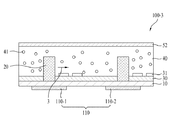
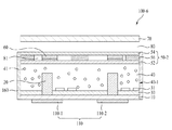
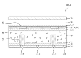
40 導光層
52 第1の光学シート
54 第2の光学シート
56 接着部材
60 光学パターン
70 拡散板
110 放熱部材
101―1〜101―n サブ光源モジュール
410―1、420―1、410―2 連結固定部
510、520、530、540 コネクター
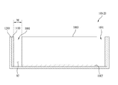
610 パッケージ本体
620 第1のリードフレーム
630 第2のリードフレーム
640 発光チップ
645 ツェナーダイオード
650 ワイヤ
712 第1の上面部
714 第1の側面部
722、724 貫通ホール
742 第2の上面部
744 第2の側面部
900 車両用ライト
910 光源モジュール
920 ライトハウジング
1801 第2の電極層
1810 電極物質層
1815 支持層
1820 ボンディング層
1825 反射層
1830 オーミック領域
1840 発光構造物
1850 パッシベーション層
1860 第1の電極層
Claims (11)
- キャビティを有するパッケージ本体;
前記キャビティに露出する第1の上面部、及び前記第1の上面部の第1の側部から折り曲げられ、前記パッケージ本体の第1の面に露出する第1の側面部を含む第1のリードフレーム;
前記キャビティに露出する第2の上面部、及び前記第2の上面部から折り曲げられ、前記パッケージ本体の前記第1の面に露出する第2の側面部を含む第2のリードフレーム;及び
第1の半導体層、活性層、及び第2の半導体層を含み、前記第1のリードフレームの前記第1の上面部上に配置される少なくとも一つの発光チップ;を含み、
前記第2の側面部は、前記パッケージ本体の前記第1の面上に露出する第1の部分及び第2の部分を含み、
前記第1の側面部は、前記第2の側面部の前記第1の部分と前記第2の側面部の前記第2の部分との間に配置され、
前記第2の上面部は、前記第1の上面部の周囲に配置され、前記キャビティに露出する第3の部分、第4の部分、及び第5の部分を含み、
前記第3の部分は、前記第1の上面部の第2の側部と向き合い、前記第1の上面部の第2の側部は、前記第1の上面部の前記第1の側部と向き合い、
前記第4の部分の一端は前記第3の部分の一端と連結され、前記第5の部分の一端は前記第3の部分の他端と連結され、
前記第4の部分の他端は前記第2の側面部の前記第1の部分と連結され、前記第5の部分の他端は前記第2の側面部の前記第2の部分と連結され、
前記第1の側面部は、前記第1の上面部の前記第1の側部と連結される上端部、及び前記上端部と連結される下端部を含み、
前記上端部の側面と前記下端部の側面は段差を有する発光素子パッケージ。 - 前記第1の上面部及び前記第1の側面部のうち少なくとも一つに少なくとも一つの第1の貫通ホールが設けられる、請求項1に記載の発光素子パッケージ。
- 前記第1のリードフレームは、前記第1の上面部と前記第1の側面部との境界部分に隣接して少なくとも一つの第1の貫通ホールを有する、請求項1に記載の発光素子パッケージ。
- 前記第1のリードフレームは、前記第1の上面部と第1の側面部とを互いに連結する各連結部分を含み、前記各連結部分の間には前記第1の貫通ホールが位置し、前記各連結部分のうち少なくとも一つの長さは残りの長さと互いに異なる、請求項2又は3に記載の発光素子パッケージ。
- 前記各連結部分は、前記発光チップに整列される第1の連結部分、及び前記発光チップに整列されない第2の連結部分を含み、
前記第1の連結部分の第1の方向の長さは、前記第2の連結部分の前記第1の方向の長さより大きく、
前記第1の方向はxyz座標系でx軸方向である、請求項4に記載の発光素子パッケージ。 - 前記下端部は前記上端部の両側面から側方向に突出する、請求項1〜5のうちいずれか1項に記載の発光素子パッケージ。
- 前記第2の連結部分と前記第1の連結部分の第1の方向の長さの比は1:1.2〜1.8であり、
前記第1の貫通ホールの前記第1の方向の長さと前記第1の側面部の前記上端部の前記第1の方向の長さとの比は1:3.8〜6.3であり、
前記第1の方向はxyz座標系でx軸方向である、請求項5に記載の発光素子パッケージ。 - 前記各連結部分のうち少なくとも一つには、前記第1の貫通ホールより直径が小さい第2の貫通ホールが設けられる、請求項4又は5に記載の発光素子パッケージ。
- 前記第1の上面部の前記第2の側部には、少なくとも一つの溝部が設けられ、
前記第2の上面部は、前記溝部に相応する第1の突出部を有する、請求項1乃至8のいずれか1項に記載の発光素子パッケージ。 - 前記少なくとも一つの発光チップは、前記第1の突出部の右側に位置する前記第1の上面部の上面の一領域に配置される第1の発光チップ、及び前記第1の突出部の左側に位置する前記第1の上面部の上面の他の領域に配置される第2の発光チップを含み、前記第1の発光チップ及び前記第2の発光チップは、600nm〜690nmの波長範囲を有する赤色光を発光し、
前記第1の発光チップと前記第1の突出部とを連結する第1のワイヤ;及び
前記第2の発光チップと前記第1の突出部とを連結する第2のワイヤ;をさらに含む、請求項9に記載の発光素子パッケージ。 - 前記第1の上面部は、前記第1の側面部を基準として前記第1の方向に突出する第2の突出部を含み、
前記第1の部分と前記第2の部分は、前記第1の側面部を基準として対称的である、請求項1乃至9のいずれか1項に記載の発光素子パッケージ。
Applications Claiming Priority (2)
| Application Number | Priority Date | Filing Date | Title |
|---|---|---|---|
| KR10-2012-0036649 | 2012-04-09 | ||
| KR1020120036649A KR101908656B1 (ko) | 2012-04-09 | 2012-04-09 | 발광 소자 패키지 |
Publications (3)
| Publication Number | Publication Date |
|---|---|
| JP2013219357A JP2013219357A (ja) | 2013-10-24 |
| JP2013219357A5 JP2013219357A5 (ja) | 2016-04-28 |
| JP6220142B2 true JP6220142B2 (ja) | 2017-10-25 |
Family
ID=48082962
Family Applications (1)
| Application Number | Title | Priority Date | Filing Date |
|---|---|---|---|
| JP2013078227A Active JP6220142B2 (ja) | 2012-04-09 | 2013-04-04 | 発光素子パッケージ |
Country Status (5)
| Country | Link |
|---|---|
| US (1) | US9171998B2 (ja) |
| EP (1) | EP2650590B1 (ja) |
| JP (1) | JP6220142B2 (ja) |
| KR (1) | KR101908656B1 (ja) |
| CN (1) | CN103367621B (ja) |
Families Citing this family (18)
| Publication number | Priority date | Publication date | Assignee | Title |
|---|---|---|---|---|
| JP6275399B2 (ja) | 2012-06-18 | 2018-02-07 | エルジー イノテック カンパニー リミテッド | 照明装置 |
| DE102013111977A1 (de) * | 2013-10-30 | 2015-04-30 | Osram Opto Semiconductors Gmbh | Optoelektronischer Halbleiterchip und Anordnung mit mindestens einem solchen optoelektronischen Halbleiterchip |
| KR101620147B1 (ko) * | 2013-12-18 | 2016-05-23 | 현대자동차주식회사 | 차량용 램프의 광원모듈 |
| KR102147940B1 (ko) * | 2013-12-27 | 2020-08-25 | 엘지이노텍 주식회사 | 조명 장치 |
| JP6374723B2 (ja) | 2014-07-25 | 2018-08-15 | スタンレー電気株式会社 | 半導体発光装置 |
| FR3027463B1 (fr) * | 2014-10-21 | 2016-12-09 | Thales Sa | Ensemble de fixation et de raccordement d'un dispositif de stockage de donnees informatiques a un calculateur embarque et procede d'utilisation associe |
| KR101684004B1 (ko) * | 2014-11-25 | 2016-12-08 | 현대자동차주식회사 | 차량용 램프의 광원모듈 |
| KR102312522B1 (ko) * | 2015-06-11 | 2021-10-15 | 삼성디스플레이 주식회사 | 표시 장치 |
| PL3106348T3 (pl) * | 2015-06-16 | 2018-08-31 | Automotive Lighting Italia S.P.A. | Światło pojazdu i odnośny sposób wytwarzania |
| US10317609B2 (en) * | 2015-11-12 | 2019-06-11 | Samsung Display Co., Ltd. | Display device |
| US10870404B2 (en) | 2016-01-11 | 2020-12-22 | SMR Patents S.à.r.l. | Elongate illuminated automotive design element, injection molded vehicle parts, and methods of manufacturing same |
| EP3741619A1 (en) * | 2016-01-11 | 2020-11-25 | SMR Patents S.à.r.l. | An elongate illuminated automotive design element |
| US20170284623A1 (en) * | 2016-03-31 | 2017-10-05 | GM Global Technology Operations LLC | Methods and apparatus for free-form illumination assemblies |
| DE102016117967A1 (de) * | 2016-09-23 | 2018-03-29 | Carl Zeiss Jena Gmbh | Leuchteinrichtung für ein Fahrzeug |
| JP7331830B2 (ja) * | 2018-03-07 | 2023-08-23 | 凸版印刷株式会社 | 光学フィルム、光学バリアフィルム、及びバックライトユニット |
| US10989387B2 (en) * | 2018-12-21 | 2021-04-27 | Valeo North America, Inc. | Automotive light device with homogeneous emitting surface |
| WO2021187535A1 (ja) * | 2020-03-19 | 2021-09-23 | 日東電工株式会社 | 光電気伝送複合モジュール |
| US20230204848A1 (en) * | 2021-12-29 | 2023-06-29 | Hyundai Mobis Co., Ltd. | Led module |
Family Cites Families (26)
| Publication number | Priority date | Publication date | Assignee | Title |
|---|---|---|---|---|
| DE4446566A1 (de) * | 1994-12-24 | 1996-06-27 | Telefunken Microelectron | Mehrpoliges, oberflächenmontierbares, elektronisches Bauelement |
| JP2003077317A (ja) * | 2001-09-03 | 2003-03-14 | Toyoda Gosei Co Ltd | Ledランプ |
| JP2005317661A (ja) * | 2004-04-27 | 2005-11-10 | Sharp Corp | 半導体発光装置およびその製造方法 |
| TWI374552B (en) * | 2004-07-27 | 2012-10-11 | Cree Inc | Ultra-thin ohmic contacts for p-type nitride light emitting devices and methods of forming |
| US7476913B2 (en) * | 2004-08-10 | 2009-01-13 | Renesas Technology Corp. | Light emitting device having a mirror portion |
| JP5038623B2 (ja) * | 2005-12-27 | 2012-10-03 | 株式会社東芝 | 光半導体装置およびその製造方法 |
| JP4830768B2 (ja) * | 2006-05-10 | 2011-12-07 | 日亜化学工業株式会社 | 半導体発光装置及び半導体発光装置の製造方法 |
| JP5057707B2 (ja) * | 2006-06-16 | 2012-10-24 | 日亜化学工業株式会社 | 発光装置 |
| JP4306772B2 (ja) * | 2006-10-05 | 2009-08-05 | 日亜化学工業株式会社 | 発光装置 |
| CN201015120Y (zh) * | 2006-10-30 | 2008-01-30 | 一诠精密工业股份有限公司 | 散热型smd发光二极管支架结构及其金属支架 |
| CN201007998Y (zh) * | 2007-01-12 | 2008-01-16 | 东贝光电科技股份有限公司 | 高功率发光二极管结构 |
| JP2009099771A (ja) * | 2007-10-17 | 2009-05-07 | Rohm Co Ltd | 半導体発光モジュール |
| JP5162280B2 (ja) * | 2008-03-06 | 2013-03-13 | ローム株式会社 | 画像読取装置の製造方法、および画像読取装置 |
| JP2009260075A (ja) * | 2008-04-17 | 2009-11-05 | Toshiba Corp | 発光装置およびリードフレーム |
| KR100986202B1 (ko) * | 2008-07-01 | 2010-10-07 | 알티전자 주식회사 | 사이드 뷰 발광 다이오드 패키지 |
| JP5444654B2 (ja) * | 2008-07-29 | 2014-03-19 | 日亜化学工業株式会社 | 発光装置 |
| KR100993903B1 (ko) * | 2008-07-31 | 2010-11-11 | 알티전자 주식회사 | 사이드 뷰 발광 다이오드 패키지 |
| US8368112B2 (en) * | 2009-01-14 | 2013-02-05 | Cree Huizhou Opto Limited | Aligned multiple emitter package |
| US8356917B2 (en) * | 2009-08-19 | 2013-01-22 | Avago Technologies Ecbu Ip (Singapore) Pte. Ltd. | Light source |
| KR101072034B1 (ko) * | 2009-10-15 | 2011-10-10 | 엘지이노텍 주식회사 | 반도체 발광소자 및 그 제조방법 |
| KR101028195B1 (ko) * | 2010-01-18 | 2011-04-11 | 엘지이노텍 주식회사 | 발광 소자 패키지 및 이를 구비한 라이트 유닛 |
| JP5383611B2 (ja) * | 2010-01-29 | 2014-01-08 | 株式会社東芝 | Ledパッケージ |
| JP5507330B2 (ja) * | 2010-04-27 | 2014-05-28 | ローム株式会社 | Ledモジュール |
| JP5528900B2 (ja) * | 2010-04-30 | 2014-06-25 | ローム株式会社 | 発光素子モジュール |
| KR101705700B1 (ko) * | 2010-07-01 | 2017-02-10 | 엘지이노텍 주식회사 | 발광 소자 |
| US9831393B2 (en) * | 2010-07-30 | 2017-11-28 | Cree Hong Kong Limited | Water resistant surface mount device package |
-
2012
- 2012-04-09 KR KR1020120036649A patent/KR101908656B1/ko active IP Right Grant
-
2013
- 2013-01-10 US US13/738,800 patent/US9171998B2/en active Active
- 2013-04-04 JP JP2013078227A patent/JP6220142B2/ja active Active
- 2013-04-08 EP EP13162721.8A patent/EP2650590B1/en active Active
- 2013-04-09 CN CN201310121670.4A patent/CN103367621B/zh active Active
Also Published As
| Publication number | Publication date |
|---|---|
| CN103367621B (zh) | 2018-03-30 |
| EP2650590A3 (en) | 2016-04-27 |
| JP2013219357A (ja) | 2013-10-24 |
| US20130264590A1 (en) | 2013-10-10 |
| US9171998B2 (en) | 2015-10-27 |
| CN103367621A (zh) | 2013-10-23 |
| KR101908656B1 (ko) | 2018-10-16 |
| EP2650590B1 (en) | 2020-08-05 |
| KR20130114369A (ko) | 2013-10-18 |
| EP2650590A2 (en) | 2013-10-16 |
Similar Documents
| Publication | Publication Date | Title |
|---|---|---|
| JP6104613B2 (ja) | 発光ランプ | |
| JP6220142B2 (ja) | 発光素子パッケージ | |
| JP6275399B2 (ja) | 照明装置 | |
| JP6282419B2 (ja) | 照明装置 | |
| JP6192987B2 (ja) | 照明装置 | |
| JP6184769B2 (ja) | 照明装置 | |
| JP6184770B2 (ja) | 照明装置 | |
| JP6230600B2 (ja) | 発光素子パッケージ | |
| KR102629830B1 (ko) | 조명장치 | |
| KR20130142035A (ko) | 조명장치 | |
| KR102071426B1 (ko) | 조명장치 | |
| KR102034226B1 (ko) | 조명장치 | |
| KR101956306B1 (ko) | 조명장치 | |
| KR20140001510A (ko) | 조명장치 | |
| KR101979723B1 (ko) | 조명장치 | |
| KR102034227B1 (ko) | 조명장치 | |
| KR20130142031A (ko) | 조명장치 | |
| KR102229782B1 (ko) | 조명장치 | |
| KR102073161B1 (ko) | 조명장치 | |
| KR101977718B1 (ko) | 조명장치 | |
| KR20140001507A (ko) | 조명장치 | |
| KR101977720B1 (ko) | 조명장치 | |
| KR20140001511A (ko) | 조명장치 | |
| KR20140001508A (ko) | 조명장치 |
Legal Events
| Date | Code | Title | Description |
|---|---|---|---|
| A521 | Request for written amendment filed |
Free format text: JAPANESE INTERMEDIATE CODE: A523 Effective date: 20160309 |
|
| A621 | Written request for application examination |
Free format text: JAPANESE INTERMEDIATE CODE: A621 Effective date: 20160309 |
|
| A977 | Report on retrieval |
Free format text: JAPANESE INTERMEDIATE CODE: A971007 Effective date: 20161219 |
|
| A131 | Notification of reasons for refusal |
Free format text: JAPANESE INTERMEDIATE CODE: A131 Effective date: 20170131 |
|
| A521 | Request for written amendment filed |
Free format text: JAPANESE INTERMEDIATE CODE: A523 Effective date: 20170426 |
|
| TRDD | Decision of grant or rejection written | ||
| A01 | Written decision to grant a patent or to grant a registration (utility model) |
Free format text: JAPANESE INTERMEDIATE CODE: A01 Effective date: 20170905 |
|
| A61 | First payment of annual fees (during grant procedure) |
Free format text: JAPANESE INTERMEDIATE CODE: A61 Effective date: 20170929 |
|
| R150 | Certificate of patent or registration of utility model |
Ref document number: 6220142 Country of ref document: JP Free format text: JAPANESE INTERMEDIATE CODE: R150 |
|
| R250 | Receipt of annual fees |
Free format text: JAPANESE INTERMEDIATE CODE: R250 |
|
| S531 | Written request for registration of change of domicile |
Free format text: JAPANESE INTERMEDIATE CODE: R313531 |
|
| S111 | Request for change of ownership or part of ownership |
Free format text: JAPANESE INTERMEDIATE CODE: R313113 |
|
| R350 | Written notification of registration of transfer |
Free format text: JAPANESE INTERMEDIATE CODE: R350 |
|
| R350 | Written notification of registration of transfer |
Free format text: JAPANESE INTERMEDIATE CODE: R350 |
|
| R250 | Receipt of annual fees |
Free format text: JAPANESE INTERMEDIATE CODE: R250 |
|
| R250 | Receipt of annual fees |
Free format text: JAPANESE INTERMEDIATE CODE: R250 |
|
| R250 | Receipt of annual fees |
Free format text: JAPANESE INTERMEDIATE CODE: R250 |