JP6200340B2 - 表示装置およびその製造方法 - Google Patents
表示装置およびその製造方法 Download PDFInfo
- Publication number
- JP6200340B2 JP6200340B2 JP2014019250A JP2014019250A JP6200340B2 JP 6200340 B2 JP6200340 B2 JP 6200340B2 JP 2014019250 A JP2014019250 A JP 2014019250A JP 2014019250 A JP2014019250 A JP 2014019250A JP 6200340 B2 JP6200340 B2 JP 6200340B2
- Authority
- JP
- Japan
- Prior art keywords
- substrate
- display device
- shielding layer
- color filter
- layer
- Prior art date
- Legal status (The legal status is an assumption and is not a legal conclusion. Google has not performed a legal analysis and makes no representation as to the accuracy of the status listed.)
- Active
Links
Images


Classifications
-
- G—PHYSICS
- G09—EDUCATION; CRYPTOGRAPHY; DISPLAY; ADVERTISING; SEALS
- G09F—DISPLAYING; ADVERTISING; SIGNS; LABELS OR NAME-PLATES; SEALS
- G09F9/00—Indicating arrangements for variable information in which the information is built-up on a support by selection or combination of individual elements
- G09F9/30—Indicating arrangements for variable information in which the information is built-up on a support by selection or combination of individual elements in which the desired character or characters are formed by combining individual elements
- G09F9/33—Indicating arrangements for variable information in which the information is built-up on a support by selection or combination of individual elements in which the desired character or characters are formed by combining individual elements being semiconductor devices, e.g. diodes
-
- H—ELECTRICITY
- H10—SEMICONDUCTOR DEVICES; ELECTRIC SOLID-STATE DEVICES NOT OTHERWISE PROVIDED FOR
- H10K—ORGANIC ELECTRIC SOLID-STATE DEVICES
- H10K59/00—Integrated devices, or assemblies of multiple devices, comprising at least one organic light-emitting element covered by group H10K50/00
- H10K59/30—Devices specially adapted for multicolour light emission
- H10K59/38—Devices specially adapted for multicolour light emission comprising colour filters or colour changing media [CCM]
-
- G—PHYSICS
- G06—COMPUTING OR CALCULATING; COUNTING
- G06F—ELECTRIC DIGITAL DATA PROCESSING
- G06F3/00—Input arrangements for transferring data to be processed into a form capable of being handled by the computer; Output arrangements for transferring data from processing unit to output unit, e.g. interface arrangements
- G06F3/01—Input arrangements or combined input and output arrangements for interaction between user and computer
- G06F3/03—Arrangements for converting the position or the displacement of a member into a coded form
- G06F3/041—Digitisers, e.g. for touch screens or touch pads, characterised by the transducing means
- G06F3/0412—Digitisers structurally integrated in a display
-
- H—ELECTRICITY
- H05—ELECTRIC TECHNIQUES NOT OTHERWISE PROVIDED FOR
- H05B—ELECTRIC HEATING; ELECTRIC LIGHT SOURCES NOT OTHERWISE PROVIDED FOR; CIRCUIT ARRANGEMENTS FOR ELECTRIC LIGHT SOURCES, IN GENERAL
- H05B33/00—Electroluminescent light sources
- H05B33/02—Details
- H05B33/04—Sealing arrangements, e.g. against humidity
-
- H—ELECTRICITY
- H05—ELECTRIC TECHNIQUES NOT OTHERWISE PROVIDED FOR
- H05B—ELECTRIC HEATING; ELECTRIC LIGHT SOURCES NOT OTHERWISE PROVIDED FOR; CIRCUIT ARRANGEMENTS FOR ELECTRIC LIGHT SOURCES, IN GENERAL
- H05B33/00—Electroluminescent light sources
- H05B33/12—Light sources with substantially two-dimensional [2D] radiating surfaces
-
- H—ELECTRICITY
- H10—SEMICONDUCTOR DEVICES; ELECTRIC SOLID-STATE DEVICES NOT OTHERWISE PROVIDED FOR
- H10K—ORGANIC ELECTRIC SOLID-STATE DEVICES
- H10K50/00—Organic light-emitting devices
- H10K50/10—OLEDs or polymer light-emitting diodes [PLED]
- H10K50/11—OLEDs or polymer light-emitting diodes [PLED] characterised by the electroluminescent [EL] layers
-
- H—ELECTRICITY
- H10—SEMICONDUCTOR DEVICES; ELECTRIC SOLID-STATE DEVICES NOT OTHERWISE PROVIDED FOR
- H10K—ORGANIC ELECTRIC SOLID-STATE DEVICES
- H10K50/00—Organic light-emitting devices
- H10K50/80—Constructional details
- H10K50/805—Electrodes
- H10K50/81—Anodes
-
- H—ELECTRICITY
- H10—SEMICONDUCTOR DEVICES; ELECTRIC SOLID-STATE DEVICES NOT OTHERWISE PROVIDED FOR
- H10K—ORGANIC ELECTRIC SOLID-STATE DEVICES
- H10K50/00—Organic light-emitting devices
- H10K50/80—Constructional details
- H10K50/805—Electrodes
- H10K50/82—Cathodes
-
- H—ELECTRICITY
- H10—SEMICONDUCTOR DEVICES; ELECTRIC SOLID-STATE DEVICES NOT OTHERWISE PROVIDED FOR
- H10K—ORGANIC ELECTRIC SOLID-STATE DEVICES
- H10K50/00—Organic light-emitting devices
- H10K50/80—Constructional details
- H10K50/84—Passivation; Containers; Encapsulations
- H10K50/842—Containers
- H10K50/8426—Peripheral sealing arrangements, e.g. adhesives, sealants
-
- H—ELECTRICITY
- H10—SEMICONDUCTOR DEVICES; ELECTRIC SOLID-STATE DEVICES NOT OTHERWISE PROVIDED FOR
- H10K—ORGANIC ELECTRIC SOLID-STATE DEVICES
- H10K59/00—Integrated devices, or assemblies of multiple devices, comprising at least one organic light-emitting element covered by group H10K50/00
- H10K59/10—OLED displays
- H10K59/12—Active-matrix OLED [AMOLED] displays
- H10K59/1201—Manufacture or treatment
-
- H—ELECTRICITY
- H10—SEMICONDUCTOR DEVICES; ELECTRIC SOLID-STATE DEVICES NOT OTHERWISE PROVIDED FOR
- H10K—ORGANIC ELECTRIC SOLID-STATE DEVICES
- H10K59/00—Integrated devices, or assemblies of multiple devices, comprising at least one organic light-emitting element covered by group H10K50/00
- H10K59/10—OLED displays
- H10K59/12—Active-matrix OLED [AMOLED] displays
- H10K59/126—Shielding, e.g. light-blocking means over the TFTs
-
- H—ELECTRICITY
- H10—SEMICONDUCTOR DEVICES; ELECTRIC SOLID-STATE DEVICES NOT OTHERWISE PROVIDED FOR
- H10K—ORGANIC ELECTRIC SOLID-STATE DEVICES
- H10K71/00—Manufacture or treatment specially adapted for the organic devices covered by this subclass
-
- H—ELECTRICITY
- H10—SEMICONDUCTOR DEVICES; ELECTRIC SOLID-STATE DEVICES NOT OTHERWISE PROVIDED FOR
- H10K—ORGANIC ELECTRIC SOLID-STATE DEVICES
- H10K77/00—Constructional details of devices covered by this subclass and not covered by groups H10K10/80, H10K30/80, H10K50/80 or H10K59/80
- H10K77/10—Substrates, e.g. flexible substrates
- H10K77/111—Flexible substrates
-
- G—PHYSICS
- G02—OPTICS
- G02B—OPTICAL ELEMENTS, SYSTEMS OR APPARATUS
- G02B5/00—Optical elements other than lenses
- G02B5/20—Filters
- G02B5/201—Filters in the form of arrays
-
- G—PHYSICS
- G06—COMPUTING OR CALCULATING; COUNTING
- G06F—ELECTRIC DIGITAL DATA PROCESSING
- G06F2203/00—Indexing scheme relating to G06F3/00 - G06F3/048
- G06F2203/041—Indexing scheme relating to G06F3/041 - G06F3/045
- G06F2203/04103—Manufacturing, i.e. details related to manufacturing processes specially suited for touch sensitive devices
-
- G—PHYSICS
- G06—COMPUTING OR CALCULATING; COUNTING
- G06F—ELECTRIC DIGITAL DATA PROCESSING
- G06F2203/00—Indexing scheme relating to G06F3/00 - G06F3/048
- G06F2203/041—Indexing scheme relating to G06F3/041 - G06F3/045
- G06F2203/04107—Shielding in digitiser, i.e. guard or shielding arrangements, mostly for capacitive touchscreens, e.g. driven shields, driven grounds
-
- H—ELECTRICITY
- H10—SEMICONDUCTOR DEVICES; ELECTRIC SOLID-STATE DEVICES NOT OTHERWISE PROVIDED FOR
- H10K—ORGANIC ELECTRIC SOLID-STATE DEVICES
- H10K2102/00—Constructional details relating to the organic devices covered by this subclass
- H10K2102/301—Details of OLEDs
- H10K2102/311—Flexible OLED
-
- H—ELECTRICITY
- H10—SEMICONDUCTOR DEVICES; ELECTRIC SOLID-STATE DEVICES NOT OTHERWISE PROVIDED FOR
- H10K—ORGANIC ELECTRIC SOLID-STATE DEVICES
- H10K59/00—Integrated devices, or assemblies of multiple devices, comprising at least one organic light-emitting element covered by group H10K50/00
- H10K59/80—Constructional details
- H10K59/805—Electrodes
- H10K59/8051—Anodes
-
- H—ELECTRICITY
- H10—SEMICONDUCTOR DEVICES; ELECTRIC SOLID-STATE DEVICES NOT OTHERWISE PROVIDED FOR
- H10K—ORGANIC ELECTRIC SOLID-STATE DEVICES
- H10K59/00—Integrated devices, or assemblies of multiple devices, comprising at least one organic light-emitting element covered by group H10K50/00
- H10K59/80—Constructional details
- H10K59/805—Electrodes
- H10K59/8052—Cathodes
-
- H—ELECTRICITY
- H10—SEMICONDUCTOR DEVICES; ELECTRIC SOLID-STATE DEVICES NOT OTHERWISE PROVIDED FOR
- H10K—ORGANIC ELECTRIC SOLID-STATE DEVICES
- H10K59/00—Integrated devices, or assemblies of multiple devices, comprising at least one organic light-emitting element covered by group H10K50/00
- H10K59/80—Constructional details
- H10K59/87—Passivation; Containers; Encapsulations
- H10K59/871—Self-supporting sealing arrangements
- H10K59/8722—Peripheral sealing arrangements, e.g. adhesives, sealants
-
- Y—GENERAL TAGGING OF NEW TECHNOLOGICAL DEVELOPMENTS; GENERAL TAGGING OF CROSS-SECTIONAL TECHNOLOGIES SPANNING OVER SEVERAL SECTIONS OF THE IPC; TECHNICAL SUBJECTS COVERED BY FORMER USPC CROSS-REFERENCE ART COLLECTIONS [XRACs] AND DIGESTS
- Y02—TECHNOLOGIES OR APPLICATIONS FOR MITIGATION OR ADAPTATION AGAINST CLIMATE CHANGE
- Y02E—REDUCTION OF GREENHOUSE GAS [GHG] EMISSIONS, RELATED TO ENERGY GENERATION, TRANSMISSION OR DISTRIBUTION
- Y02E10/00—Energy generation through renewable energy sources
- Y02E10/50—Photovoltaic [PV] energy
- Y02E10/549—Organic PV cells
Landscapes
- Engineering & Computer Science (AREA)
- Physics & Mathematics (AREA)
- Optics & Photonics (AREA)
- Theoretical Computer Science (AREA)
- General Engineering & Computer Science (AREA)
- General Physics & Mathematics (AREA)
- Human Computer Interaction (AREA)
- Microelectronics & Electronic Packaging (AREA)
- Manufacturing & Machinery (AREA)
- Electroluminescent Light Sources (AREA)
- Position Input By Displaying (AREA)
- Devices For Indicating Variable Information By Combining Individual Elements (AREA)
Description
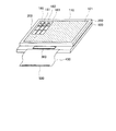
図1乃至4を用いて、本発明の実施形態1に係る表示装置の構成を説明する。図1は、本発明の実施形態1における表示装置の斜視図を示す図である。また、図2は、本発明の実施形態1における表示装置の平面図を示す図である。実施形態1では、高精細化に有利な「白色+CF構造」の表示装置について説明する。
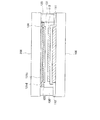
図5乃至8を用いて、本発明の実施形態2に係る表示装置の構成を説明する。図5は、本発明の実施形態2における表示装置の平面図を示す図である。また、図7は、本発明の実施形態2における表示装置のC−D断面図を示す図である。実施形態2でも、実施形態1と同様に高精細化に有利な「白色+CF構造」の表示装置について説明する。
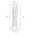
図9を用いて、本発明の実施形態3に係る表示装置の構成を説明する。図9は、本発明の実施形態3における表示装置の断面図を示す図である。図9と図3との相違点は、図9は対向基板200の基板100とは反対の面200aに第2遮光層141と透明導電層142とが配置されている点である。第2遮光層141は周辺領域120の一部に配置されており、透明導電層142は表示領域110に配置されている。図9に示すように、透明導電層142はストライプ状に配置され、タッチセンサ用配線を構成してもよい。また、第2遮光層141および透明導電層142は保護層143で覆われていてもよい。また、第2遮光層141を導電材料で形成し、タッチセンサ用配線の一部として使用してもよい。タッチセンサ用の配線を遮光層として用いることで、レーザ光照射時に問題となる温度上昇に対しての放熱効果が期待できる。
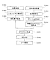
図10〜12を用いて、本発明の実施形態4に係る表示装置の製造方法を説明する。図10は、本発明の実施形態4における表示装置の製造方法のプロセスフローを示す図である。図10を用いて、本発明に係る表示装置の製造方法を説明する。
110:表示領域
111:トランジスタ層
112:層間絶縁層
113:発光素子
120:周辺領域
121:遮光層
121a:遮光層121の基板100に対向する上面
121b:遮光層121の端部
121c:表示領域110を含む領域に対応する遮光層
121d:周辺領域120に対応する遮光層
122、181、182、183:カラーフィルタ
122a:カラーフィルタ122の基板100に対向する上面
122b:カラーフィルタ122の端部
123:無機パッシベーション層
124:スリット
130:ガラスフリット
131:空隙部
141:第2遮光層
142:透明導電層
143:保護層
150:マスク
160、170:レーザ
180:画素
200:対向基板
200a:対向基板200の基板100とは反対の面
300:ドライバIC
400:FPC
500:端子部
Claims (22)
- 複数の画素のそれぞれに発光素子が設けられ、前記画素が配列された表示領域を有する第1基板と、
前記画素を開口する遮光層、および、着色層を有し少なくとも前記遮光層の開口部に設けられたカラーフィルタを有する第2基板と、
ガラスを含み、前記表示領域および前記カラーフィルタが対向するように、前記第1基板および前記第2基板を貼り合わせ、前記カラーフィルタの外側に設けられたシール材と、
少なくとも前記カラーフィルタの前記第1基板側の面および端部を覆う無機絶縁層と、を有し、
前記遮光層は、黒色の樹脂材料であり、
前記カラーフィルタは、前記遮光層の前記第1基板側に設けられ、
前記無機絶縁層は、前記シール材と接し、前記第2基板と前記シール材との間、前記遮光層の側方、および前記カラーフィルタの側方に設けられ、
前記無機絶縁層は、第1表面および前記第1表面の反対側の第2表面を有し、
前記シール材は、前記第1表面において前記無機絶縁層と接し、
前記第2基板は、前記第2表面において前記無機絶縁層と接し、
前記遮光層の前記第2基板側の面と前記無機絶縁層の前記第2表面とは一致し、
前記シール材は、平面視において前記第2基板と重畳することを特徴とする表示装置。 - 前記無機絶縁層は、前記カラーフィルタの前記第1基板側の面と接していることを特徴とする請求項1に記載の表示装置。
- 前記第1基板、前記第2基板および前記シール材で囲まれた空隙部に、前記発光素子が露出されていることを特徴とする請求項1に記載の表示装置。
- 前記第2基板は透明であることを特徴とする請求項1に記載の表示装置。
- 前記空隙部には、露点が−70℃以下の気体が含まれていることを特徴とする請求項3に記載の表示装置。
- 前記空隙部には、酸素濃度が1ppm以下の気体が含まれていることを特徴とする請求項5に記載の表示装置。
- 複数の画素のそれぞれに発光素子が設けられ、前記画素が配列された表示領域を有する第1基板と、
前記第1基板に対向する透明な第2基板と、
前記第1基板と前記第2基板との間に設けられ、前記画素に対応して設けられた開口部および前記表示領域の周辺の周辺領域に設けられたスリットの両方を有する遮光層と、
ガラスを含み、前記表示領域および前記遮光層の開口部が対向するように前記第1基板および前記第2基板を貼り合わせるシール材と、
前記遮光層の前記第1基板側の面および側方、ならびに前記スリットの内部に設けられた無機絶縁層と、
を有することを特徴とする表示装置。 - 前記無機絶縁層は、前記遮光層の前記第1基板側の面と接していることを特徴とする請求項7に記載の表示装置。
- 前記スリットは前記表示領域を囲むように連続して設けられていることを特徴とする請求項7に記載の表示装置。
- 前記第2基板に配置され、着色層を有し、少なくとも前記遮光層の開口部に設けられたカラーフィルタと、
少なくとも前記カラーフィルタの上面および端部を覆う無機絶縁層と、を有することを特徴とする請求項9に記載の表示装置。 - 前記第1基板、前記第2基板および前記シール材で囲まれた空隙部に、前記発光素子が露出されていることを特徴とする請求項10に記載の表示装置。
- 前記シール材は、前記無機絶縁層と接していることを特徴とする請求項11に記載の表示装置。
- 前記空隙部には、露点が−70℃以下の気体が含まれていることを特徴とする請求項11または12に記載の表示装置。
- 前記空隙部には、酸素濃度が1ppm以下の気体が含まれていることを特徴とする請求項13に記載の表示装置。
- 複数の画素のそれぞれに発光素子が設けられ、前記画素が配列された表示領域を有する第1基板と、
前記第1基板に対向する透明な、かつ、カラーフィルタを有する第2基板と、
前記第1基板と前記第2基板との間に設けられ、前記画素を開口する第1遮光層と、
前記第2基板に対して前記第1遮光層が配置された面とは反対の面に配置され、前記表示領域の周辺の周辺領域に設けられた第2遮光層と、
少なくとも前記カラーフィルタの前記第1基板側の面および端部を覆う無機絶縁層と、
ガラスを含み、前記表示領域および前記カラーフィルタが対向するように前記第1基板および前記第2基板を貼り合わせるシール材と、を有し、
前記第1遮光層は、黒色の樹脂材料であり、
前記カラーフィルタは、前記第1遮光層の前記第1基板側に設けられ、
前記無機絶縁層は、前記第1遮光層の側方および前記カラーフィルタの側方に設けられ、
前記第1遮光層の前記第2基板側の面と前記無機絶縁層の前記第2基板側の面とは一致することを特徴とする表示装置。 - 前記無機絶縁層は、前記カラーフィルタの前記第1基板側の面と接していることを特徴とする請求項15に記載の表示装置。
- 前記第2遮光層は前記表示領域を囲むように連続して設けられていることを特徴とする請求項15に記載の表示装置。
- 前記第2遮光層が配置された面であって、前記表示領域に透明導電層を有することを特徴とする請求項15乃至17のいずれか一に記載の表示装置。
- 前記透明導電層はタッチセンサ用配線であることを特徴とする請求項18に記載の表示装置。
- 前記スリットは、平面視において前記発光素子と前記シール材との間に挟まれていることを特徴とする請求項7に記載の表示装置。
- 前記シール材、前記無機絶縁層、および前記第2基板は、平面視において互いに重畳し、
前記無機絶縁層は、前記シール材と前記第2基板との間に設けられていることを特徴とする請求項1に記載の表示装置。 - 前記第2基板は、平面視において前記第2基板が前記シール材と重畳する領域に開口が設けられていないことを特徴とする請求項7または15に記載の表示装置。
Priority Applications (6)
| Application Number | Priority Date | Filing Date | Title |
|---|---|---|---|
| JP2014019250A JP6200340B2 (ja) | 2014-02-04 | 2014-02-04 | 表示装置およびその製造方法 |
| TW104100432A TWI557902B (zh) | 2014-02-04 | 2015-01-07 | Display device |
| KR1020150008467A KR101701020B1 (ko) | 2014-02-04 | 2015-01-19 | 표시장치 |
| CN201510029030.XA CN104821139B (zh) | 2014-02-04 | 2015-01-21 | 显示装置 |
| US14/606,658 US9603204B2 (en) | 2014-02-04 | 2015-01-27 | Display device |
| US15/413,529 US9978985B2 (en) | 2014-02-04 | 2017-01-24 | Display device |
Applications Claiming Priority (1)
| Application Number | Priority Date | Filing Date | Title |
|---|---|---|---|
| JP2014019250A JP6200340B2 (ja) | 2014-02-04 | 2014-02-04 | 表示装置およびその製造方法 |
Publications (3)
| Publication Number | Publication Date |
|---|---|
| JP2015146286A JP2015146286A (ja) | 2015-08-13 |
| JP2015146286A5 JP2015146286A5 (ja) | 2017-02-09 |
| JP6200340B2 true JP6200340B2 (ja) | 2017-09-20 |
Family
ID=53731417
Family Applications (1)
| Application Number | Title | Priority Date | Filing Date |
|---|---|---|---|
| JP2014019250A Active JP6200340B2 (ja) | 2014-02-04 | 2014-02-04 | 表示装置およびその製造方法 |
Country Status (5)
| Country | Link |
|---|---|
| US (2) | US9603204B2 (ja) |
| JP (1) | JP6200340B2 (ja) |
| KR (1) | KR101701020B1 (ja) |
| CN (1) | CN104821139B (ja) |
| TW (1) | TWI557902B (ja) |
Families Citing this family (19)
| Publication number | Priority date | Publication date | Assignee | Title |
|---|---|---|---|---|
| TWI570909B (zh) * | 2016-01-07 | 2017-02-11 | 友達光電股份有限公司 | 有機發光顯示面板 |
| US10042198B2 (en) * | 2016-01-29 | 2018-08-07 | Panasonic Liquid Crystal Display Co., Ltd. | Liquid crystal display device |
| KR102544245B1 (ko) | 2016-02-19 | 2023-06-16 | 삼성전자주식회사 | 그래픽 효과 적용 방법 및 이를 수행하는 전자 장치 |
| KR102610710B1 (ko) * | 2016-06-10 | 2023-12-08 | 삼성디스플레이 주식회사 | 표시 장치 및 그의 제조방법 |
| CN106159117A (zh) * | 2016-09-14 | 2016-11-23 | Tcl集团股份有限公司 | 一种提高qled器件稳定性的封装方法及封装结构 |
| KR102673721B1 (ko) * | 2016-11-07 | 2024-06-11 | 삼성전자주식회사 | Led 패널 및 그 제조 방법 |
| CN107092126B (zh) * | 2017-06-26 | 2020-01-03 | 京东方科技集团股份有限公司 | 一种显示面板、显示装置 |
| CN107331692B (zh) * | 2017-08-25 | 2019-09-17 | 深圳市华星光电半导体显示技术有限公司 | Oled显示面板及其制作方法 |
| JP7067185B2 (ja) * | 2018-03-27 | 2022-05-16 | セイコーエプソン株式会社 | 表示装置 |
| CN109346617B (zh) * | 2018-08-28 | 2020-08-25 | 信利半导体有限公司 | 全彩oled显示器 |
| CN109585681B (zh) | 2018-12-05 | 2021-01-22 | 京东方科技集团股份有限公司 | 一种显示面板及其封装方法、以及显示装置 |
| CN109376714A (zh) * | 2018-12-13 | 2019-02-22 | 固安翌光科技有限公司 | 一种指纹识别模组及其制备方法 |
| US12029100B2 (en) * | 2019-04-19 | 2024-07-02 | Sharp Kabushiki Kaisha | Method for manufacturing display device |
| JP7263120B2 (ja) | 2019-05-23 | 2023-04-24 | 株式会社ジャパンディスプレイ | 表示装置及び表示パネル |
| CN110275650B (zh) | 2019-06-27 | 2022-03-29 | 昆山国显光电有限公司 | 触摸感应装置、触控显示面板及触控显示面板母板 |
| KR102869778B1 (ko) * | 2019-08-02 | 2025-10-14 | 삼성디스플레이 주식회사 | 전자 패널 및 이를 포함하는 전자 장치 |
| CN110703946B (zh) * | 2019-09-30 | 2024-05-07 | 武汉天马微电子有限公司 | 显示面板和显示装置 |
| WO2021117364A1 (ja) * | 2019-12-10 | 2021-06-17 | ソニーグループ株式会社 | 表示装置および電子機器 |
| JP7434037B2 (ja) * | 2020-04-03 | 2024-02-20 | 株式会社ジャパンディスプレイ | 発光素子の実装方法および表示装置 |
Family Cites Families (24)
| Publication number | Priority date | Publication date | Assignee | Title |
|---|---|---|---|---|
| US6879319B2 (en) * | 2002-10-25 | 2005-04-12 | Eastman Kodak Company | Integrated OLED display and touch screen |
| KR20060059873A (ko) * | 2003-08-22 | 2006-06-02 | 코니카 미놀타 옵토 인코포레이티드 | 고체 촬상 장치 및 상기 고체 촬상 장치를 구비한 촬상장치 및 고체 촬상 장치의 마이크로렌즈 어레이 제조 방법 |
| US7132801B2 (en) * | 2003-12-15 | 2006-11-07 | Lg.Philips Lcd Co., Ltd. | Dual panel-type organic electroluminescent device and method for fabricating the same |
| US20050248270A1 (en) * | 2004-05-05 | 2005-11-10 | Eastman Kodak Company | Encapsulating OLED devices |
| JP4175298B2 (ja) * | 2004-07-07 | 2008-11-05 | セイコーエプソン株式会社 | カラーフィルタとその製造方法及び電気光学装置並びに電子機器 |
| US20070003743A1 (en) * | 2004-08-27 | 2007-01-04 | Masaaki Asano | Color filter substrate for organic EL element |
| US20070002192A1 (en) * | 2005-06-29 | 2007-01-04 | Casio Computer Co., Ltd. | Liquid crystal display apparatus including touch panel |
| JP5194339B2 (ja) * | 2005-06-29 | 2013-05-08 | カシオ計算機株式会社 | 液晶表示素子 |
| WO2007046170A1 (ja) * | 2005-10-18 | 2007-04-26 | Sharp Kabushiki Kaisha | カラーフィルタ基板及びそれを用いた表示装置 |
| KR100673765B1 (ko) | 2006-01-20 | 2007-01-24 | 삼성에스디아이 주식회사 | 유기전계발광 표시장치 및 그 제조방법 |
| JP2009151945A (ja) * | 2007-12-18 | 2009-07-09 | Fuji Electric Holdings Co Ltd | 有機el発光デバイスおよびその製造方法 |
| JP2009252687A (ja) * | 2008-04-10 | 2009-10-29 | Seiko Epson Corp | 有機エレクトロルミネッセンス装置の製造方法及び有機エレクトロルミネッセンス装置 |
| JP2010027266A (ja) * | 2008-07-16 | 2010-02-04 | Seiko Epson Corp | 電気光学装置及び電子機器 |
| TWI413249B (zh) * | 2008-10-22 | 2013-10-21 | Wintek Corp | 有機發光二極體顯示裝置及其製造方法 |
| JP2011065896A (ja) * | 2009-09-17 | 2011-03-31 | Toshiba Corp | 電子デバイスの製造方法 |
| JP2011165422A (ja) * | 2010-02-08 | 2011-08-25 | Toppan Printing Co Ltd | トップエミッション型有機elディスプレイ及びその製造方法並びにそれに用いる色フィルター |
| CN102754524B (zh) * | 2010-07-23 | 2015-09-02 | 株式会社日本有机雷特显示器 | 显示面板及其制造方法 |
| KR101920374B1 (ko) * | 2011-04-27 | 2018-11-20 | 가부시키가이샤 한도오따이 에네루기 켄큐쇼 | 발광 장치 및 그 제작 방법 |
| KR101917753B1 (ko) * | 2011-06-24 | 2018-11-13 | 가부시키가이샤 한도오따이 에네루기 켄큐쇼 | 표시 장치 |
| JP2013069480A (ja) * | 2011-09-21 | 2013-04-18 | Semiconductor Energy Lab Co Ltd | 発光装置、電子機器、及び照明装置 |
| JP5949029B2 (ja) * | 2012-03-26 | 2016-07-06 | 大日本印刷株式会社 | 表示装置用前面保護板、及び表示装置 |
| JP6415798B2 (ja) * | 2012-04-05 | 2018-10-31 | 大日本印刷株式会社 | 表示装置用前面保護板、及び表示装置 |
| KR101989940B1 (ko) * | 2012-05-11 | 2019-06-17 | 가부시키가이샤 한도오따이 에네루기 켄큐쇼 | 발광 장치 및 발광 장치의 제작 방법 |
| US9444059B2 (en) * | 2013-02-21 | 2016-09-13 | Semiconductor Energy Laboratory Co., Ltd. | Organometallic complex, light-emitting element, light-emitting device, electronic device, and lighting device |
-
2014
- 2014-02-04 JP JP2014019250A patent/JP6200340B2/ja active Active
-
2015
- 2015-01-07 TW TW104100432A patent/TWI557902B/zh active
- 2015-01-19 KR KR1020150008467A patent/KR101701020B1/ko active Active
- 2015-01-21 CN CN201510029030.XA patent/CN104821139B/zh active Active
- 2015-01-27 US US14/606,658 patent/US9603204B2/en active Active
-
2017
- 2017-01-24 US US15/413,529 patent/US9978985B2/en active Active
Also Published As
| Publication number | Publication date |
|---|---|
| US20150223297A1 (en) | 2015-08-06 |
| JP2015146286A (ja) | 2015-08-13 |
| TW201532267A (zh) | 2015-08-16 |
| US9978985B2 (en) | 2018-05-22 |
| US20170133627A1 (en) | 2017-05-11 |
| US9603204B2 (en) | 2017-03-21 |
| KR101701020B1 (ko) | 2017-02-13 |
| KR20150091982A (ko) | 2015-08-12 |
| CN104821139B (zh) | 2018-10-26 |
| CN104821139A (zh) | 2015-08-05 |
| TWI557902B (zh) | 2016-11-11 |
Similar Documents
| Publication | Publication Date | Title |
|---|---|---|
| JP6200340B2 (ja) | 表示装置およびその製造方法 | |
| KR102364863B1 (ko) | 표시 장치 및 그 제조 방법 | |
| JP6135062B2 (ja) | 発光装置、発光装置の製造方法、電子機器 | |
| CN101287314B (zh) | 显示装置及其制造方法 | |
| KR101823962B1 (ko) | 유기 el 장치, 유기 el 장치의 제조 방법 및, 전자 기기 | |
| KR102614612B1 (ko) | 관통홀을 통해 기판의 앞면과 배면을 연결한 평판 표시장치 | |
| KR102495122B1 (ko) | 표시 장치 | |
| US9853249B2 (en) | Display device including reflecting layer | |
| TWI542931B (zh) | 畫素結構之修補方法、修補後之畫素結構以及畫素陣列 | |
| JP2015141749A (ja) | 表示装置およびその製造方法 | |
| KR101753771B1 (ko) | 평판 표시 장치 및 그 제조방법 | |
| KR20240149380A (ko) | 가요성 표시 장치 및 이의 제조 방법 | |
| US9439248B2 (en) | Electroluminescent display screen and method for preparing the same, and display device | |
| KR102799461B1 (ko) | 표시 장치 | |
| JP6574230B2 (ja) | 白色発光領域を含むディスプレイ装置 | |
| KR102570551B1 (ko) | 디스플레이 장치 | |
| JP7077001B2 (ja) | 表示装置 | |
| JP2017071842A (ja) | 成膜用マスク及びそれを用いた成膜方法 | |
| TWM512144U (zh) | 顯示面板 | |
| JP2016001526A (ja) | 表示装置 | |
| JP2009031393A (ja) | 電子装置及び光共振器 | |
| TWI570909B (zh) | 有機發光顯示面板 | |
| JP2016219199A (ja) | 有機el装置の製造方法 | |
| JP2015198032A (ja) | 有機エレクトロルミネッセンス装置の製造方法 | |
| JP2010272273A (ja) | 有機el装置の製造方法 |
Legal Events
| Date | Code | Title | Description |
|---|---|---|---|
| A521 | Request for written amendment filed |
Free format text: JAPANESE INTERMEDIATE CODE: A523 Effective date: 20161222 |
|
| A621 | Written request for application examination |
Free format text: JAPANESE INTERMEDIATE CODE: A621 Effective date: 20161222 |
|
| A871 | Explanation of circumstances concerning accelerated examination |
Free format text: JAPANESE INTERMEDIATE CODE: A871 Effective date: 20161222 |
|
| A975 | Report on accelerated examination |
Free format text: JAPANESE INTERMEDIATE CODE: A971005 Effective date: 20170317 |
|
| A131 | Notification of reasons for refusal |
Free format text: JAPANESE INTERMEDIATE CODE: A131 Effective date: 20170328 |
|
| A521 | Request for written amendment filed |
Free format text: JAPANESE INTERMEDIATE CODE: A523 Effective date: 20170525 |
|
| TRDD | Decision of grant or rejection written | ||
| A01 | Written decision to grant a patent or to grant a registration (utility model) |
Free format text: JAPANESE INTERMEDIATE CODE: A01 Effective date: 20170801 |
|
| A61 | First payment of annual fees (during grant procedure) |
Free format text: JAPANESE INTERMEDIATE CODE: A61 Effective date: 20170825 |
|
| R150 | Certificate of patent or registration of utility model |
Ref document number: 6200340 Country of ref document: JP Free format text: JAPANESE INTERMEDIATE CODE: R150 |
|
| R250 | Receipt of annual fees |
Free format text: JAPANESE INTERMEDIATE CODE: R250 |
|
| R250 | Receipt of annual fees |
Free format text: JAPANESE INTERMEDIATE CODE: R250 |
|
| R250 | Receipt of annual fees |
Free format text: JAPANESE INTERMEDIATE CODE: R250 |
|
| R250 | Receipt of annual fees |
Free format text: JAPANESE INTERMEDIATE CODE: R250 |
|
| R250 | Receipt of annual fees |
Free format text: JAPANESE INTERMEDIATE CODE: R250 |
|
| S111 | Request for change of ownership or part of ownership |
Free format text: JAPANESE INTERMEDIATE CODE: R313113 |
|
| R350 | Written notification of registration of transfer |
Free format text: JAPANESE INTERMEDIATE CODE: R350 |
|
| R250 | Receipt of annual fees |
Free format text: JAPANESE INTERMEDIATE CODE: R250 |