JP6191728B2 - Image sensor module - Google Patents
Image sensor module Download PDFInfo
- Publication number
- JP6191728B2 JP6191728B2 JP2016101074A JP2016101074A JP6191728B2 JP 6191728 B2 JP6191728 B2 JP 6191728B2 JP 2016101074 A JP2016101074 A JP 2016101074A JP 2016101074 A JP2016101074 A JP 2016101074A JP 6191728 B2 JP6191728 B2 JP 6191728B2
- Authority
- JP
- Japan
- Prior art keywords
- image sensor
- interposer substrate
- sensor module
- holes
- electrode
- Prior art date
- Legal status (The legal status is an assumption and is not a legal conclusion. Google has not performed a legal analysis and makes no representation as to the accuracy of the status listed.)
- Active
Links
- 239000000758 substrate Substances 0.000 claims description 133
- 238000003384 imaging method Methods 0.000 claims description 38
- 230000031700 light absorption Effects 0.000 claims description 24
- 239000011347 resin Substances 0.000 claims description 14
- 229920005989 resin Polymers 0.000 claims description 14
- 238000006243 chemical reaction Methods 0.000 claims description 9
- 239000004020 conductor Substances 0.000 claims description 2
- 230000000149 penetrating effect Effects 0.000 claims 1
- 239000010410 layer Substances 0.000 description 50
- 238000000034 method Methods 0.000 description 27
- 230000003287 optical effect Effects 0.000 description 22
- 229910052751 metal Inorganic materials 0.000 description 14
- 239000002184 metal Substances 0.000 description 14
- 238000007747 plating Methods 0.000 description 14
- 239000011342 resin composition Substances 0.000 description 8
- 238000004519 manufacturing process Methods 0.000 description 7
- 239000000463 material Substances 0.000 description 6
- 239000000049 pigment Substances 0.000 description 6
- 239000011521 glass Substances 0.000 description 5
- VEXZGXHMUGYJMC-UHFFFAOYSA-N Hydrochloric acid Chemical compound Cl VEXZGXHMUGYJMC-UHFFFAOYSA-N 0.000 description 4
- RTAQQCXQSZGOHL-UHFFFAOYSA-N Titanium Chemical compound [Ti] RTAQQCXQSZGOHL-UHFFFAOYSA-N 0.000 description 4
- 230000015572 biosynthetic process Effects 0.000 description 4
- 230000001788 irregular Effects 0.000 description 4
- 239000000203 mixture Substances 0.000 description 4
- 229910000679 solder Inorganic materials 0.000 description 4
- 238000004544 sputter deposition Methods 0.000 description 4
- 239000010936 titanium Substances 0.000 description 4
- 229910052719 titanium Inorganic materials 0.000 description 4
- 238000007740 vapor deposition Methods 0.000 description 4
- 238000001039 wet etching Methods 0.000 description 4
- PXHVJJICTQNCMI-UHFFFAOYSA-N Nickel Chemical compound [Ni] PXHVJJICTQNCMI-UHFFFAOYSA-N 0.000 description 3
- 230000009977 dual effect Effects 0.000 description 3
- 238000007772 electroless plating Methods 0.000 description 3
- 238000009713 electroplating Methods 0.000 description 3
- 230000035515 penetration Effects 0.000 description 3
- KRHYYFGTRYWZRS-UHFFFAOYSA-N Fluorane Chemical compound F KRHYYFGTRYWZRS-UHFFFAOYSA-N 0.000 description 2
- UQSXHKLRYXJYBZ-UHFFFAOYSA-N Iron oxide Chemical compound [Fe]=O UQSXHKLRYXJYBZ-UHFFFAOYSA-N 0.000 description 2
- QAOWNCQODCNURD-UHFFFAOYSA-N Sulfuric acid Chemical compound OS(O)(=O)=O QAOWNCQODCNURD-UHFFFAOYSA-N 0.000 description 2
- MCMNRKCIXSYSNV-UHFFFAOYSA-N Zirconium dioxide Chemical compound O=[Zr]=O MCMNRKCIXSYSNV-UHFFFAOYSA-N 0.000 description 2
- 239000006229 carbon black Substances 0.000 description 2
- 239000010949 copper Substances 0.000 description 2
- 238000001312 dry etching Methods 0.000 description 2
- 238000005530 etching Methods 0.000 description 2
- -1 for example Substances 0.000 description 2
- 239000010931 gold Substances 0.000 description 2
- 230000002093 peripheral effect Effects 0.000 description 2
- 238000001020 plasma etching Methods 0.000 description 2
- 239000011241 protective layer Substances 0.000 description 2
- 239000004065 semiconductor Substances 0.000 description 2
- FWLHAQYOFMQTHQ-UHFFFAOYSA-N 2-N-[8-[[8-(4-aminoanilino)-10-phenylphenazin-10-ium-2-yl]amino]-10-phenylphenazin-10-ium-2-yl]-8-N,10-diphenylphenazin-10-ium-2,8-diamine hydroxy-oxido-dioxochromium Chemical compound O[Cr]([O-])(=O)=O.O[Cr]([O-])(=O)=O.O[Cr]([O-])(=O)=O.Nc1ccc(Nc2ccc3nc4ccc(Nc5ccc6nc7ccc(Nc8ccc9nc%10ccc(Nc%11ccccc%11)cc%10[n+](-c%10ccccc%10)c9c8)cc7[n+](-c7ccccc7)c6c5)cc4[n+](-c4ccccc4)c3c2)cc1 FWLHAQYOFMQTHQ-UHFFFAOYSA-N 0.000 description 1
- 229910018072 Al 2 O 3 Inorganic materials 0.000 description 1
- PIGFYZPCRLYGLF-UHFFFAOYSA-N Aluminum nitride Chemical compound [Al]#N PIGFYZPCRLYGLF-UHFFFAOYSA-N 0.000 description 1
- 238000009623 Bosch process Methods 0.000 description 1
- OKTJSMMVPCPJKN-UHFFFAOYSA-N Carbon Chemical compound [C] OKTJSMMVPCPJKN-UHFFFAOYSA-N 0.000 description 1
- RYGMFSIKBFXOCR-UHFFFAOYSA-N Copper Chemical compound [Cu] RYGMFSIKBFXOCR-UHFFFAOYSA-N 0.000 description 1
- 239000004593 Epoxy Substances 0.000 description 1
- GRYLNZFGIOXLOG-UHFFFAOYSA-N Nitric acid Chemical compound O[N+]([O-])=O GRYLNZFGIOXLOG-UHFFFAOYSA-N 0.000 description 1
- VYPSYNLAJGMNEJ-UHFFFAOYSA-N Silicium dioxide Chemical compound O=[Si]=O VYPSYNLAJGMNEJ-UHFFFAOYSA-N 0.000 description 1
- CDBYLPFSWZWCQE-UHFFFAOYSA-L Sodium Carbonate Chemical compound [Na+].[Na+].[O-]C([O-])=O CDBYLPFSWZWCQE-UHFFFAOYSA-L 0.000 description 1
- GWEVSGVZZGPLCZ-UHFFFAOYSA-N Titan oxide Chemical compound O=[Ti]=O GWEVSGVZZGPLCZ-UHFFFAOYSA-N 0.000 description 1
- 239000006230 acetylene black Substances 0.000 description 1
- PNEYBMLMFCGWSK-UHFFFAOYSA-N aluminium oxide Inorganic materials [O-2].[O-2].[O-2].[Al+3].[Al+3] PNEYBMLMFCGWSK-UHFFFAOYSA-N 0.000 description 1
- 239000005354 aluminosilicate glass Substances 0.000 description 1
- 239000005388 borosilicate glass Substances 0.000 description 1
- 239000003054 catalyst Substances 0.000 description 1
- 239000000919 ceramic Substances 0.000 description 1
- 239000003086 colorant Substances 0.000 description 1
- 229910052802 copper Inorganic materials 0.000 description 1
- 238000000708 deep reactive-ion etching Methods 0.000 description 1
- 230000007547 defect Effects 0.000 description 1
- 238000010586 diagram Methods 0.000 description 1
- 238000007598 dipping method Methods 0.000 description 1
- PCHJSUWPFVWCPO-UHFFFAOYSA-N gold Chemical compound [Au] PCHJSUWPFVWCPO-UHFFFAOYSA-N 0.000 description 1
- 229910052737 gold Inorganic materials 0.000 description 1
- 230000017525 heat dissipation Effects 0.000 description 1
- 229910000040 hydrogen fluoride Inorganic materials 0.000 description 1
- 239000003999 initiator Substances 0.000 description 1
- 239000011810 insulating material Substances 0.000 description 1
- 230000003993 interaction Effects 0.000 description 1
- 238000000608 laser ablation Methods 0.000 description 1
- 239000011159 matrix material Substances 0.000 description 1
- 229910044991 metal oxide Inorganic materials 0.000 description 1
- 150000004706 metal oxides Chemical class 0.000 description 1
- 239000000178 monomer Substances 0.000 description 1
- 229910052759 nickel Inorganic materials 0.000 description 1
- 229910017604 nitric acid Inorganic materials 0.000 description 1
- 239000012860 organic pigment Substances 0.000 description 1
- 238000000059 patterning Methods 0.000 description 1
- IEQIEDJGQAUEQZ-UHFFFAOYSA-N phthalocyanine Chemical compound N1C(N=C2C3=CC=CC=C3C(N=C3C4=CC=CC=C4C(=N4)N3)=N2)=C(C=CC=C2)C2=C1N=C1C2=CC=CC=C2C4=N1 IEQIEDJGQAUEQZ-UHFFFAOYSA-N 0.000 description 1
- 229920000767 polyaniline Polymers 0.000 description 1
- 229920001721 polyimide Polymers 0.000 description 1
- 239000009719 polyimide resin Substances 0.000 description 1
- 229920000642 polymer Polymers 0.000 description 1
- 230000011514 reflex Effects 0.000 description 1
- 238000005488 sandblasting Methods 0.000 description 1
- 229910052594 sapphire Inorganic materials 0.000 description 1
- 239000010980 sapphire Substances 0.000 description 1
- 239000005368 silicate glass Substances 0.000 description 1
- HBMJWWWQQXIZIP-UHFFFAOYSA-N silicon carbide Chemical compound [Si+]#[C-] HBMJWWWQQXIZIP-UHFFFAOYSA-N 0.000 description 1
- 239000002904 solvent Substances 0.000 description 1
- OGIDPMRJRNCKJF-UHFFFAOYSA-N titanium oxide Inorganic materials [Ti]=O OGIDPMRJRNCKJF-UHFFFAOYSA-N 0.000 description 1
- XLYOFNOQVPJJNP-UHFFFAOYSA-N water Substances O XLYOFNOQVPJJNP-UHFFFAOYSA-N 0.000 description 1
Images


Classifications
-
- H—ELECTRICITY
- H04—ELECTRIC COMMUNICATION TECHNIQUE
- H04N—PICTORIAL COMMUNICATION, e.g. TELEVISION
- H04N23/00—Cameras or camera modules comprising electronic image sensors; Control thereof
- H04N23/57—Mechanical or electrical details of cameras or camera modules specially adapted for being embedded in other devices
-
- G—PHYSICS
- G02—OPTICS
- G02B—OPTICAL ELEMENTS, SYSTEMS OR APPARATUS
- G02B7/00—Mountings, adjusting means, or light-tight connections, for optical elements
- G02B7/02—Mountings, adjusting means, or light-tight connections, for optical elements for lenses
- G02B7/04—Mountings, adjusting means, or light-tight connections, for optical elements for lenses with mechanism for focusing or varying magnification
- G02B7/08—Mountings, adjusting means, or light-tight connections, for optical elements for lenses with mechanism for focusing or varying magnification adapted to co-operate with a remote control mechanism
-
- H—ELECTRICITY
- H01—ELECTRIC ELEMENTS
- H01L—SEMICONDUCTOR DEVICES NOT COVERED BY CLASS H10
- H01L27/00—Devices consisting of a plurality of semiconductor or other solid-state components formed in or on a common substrate
- H01L27/14—Devices consisting of a plurality of semiconductor or other solid-state components formed in or on a common substrate including semiconductor components sensitive to infrared radiation, light, electromagnetic radiation of shorter wavelength or corpuscular radiation and specially adapted either for the conversion of the energy of such radiation into electrical energy or for the control of electrical energy by such radiation
- H01L27/144—Devices controlled by radiation
- H01L27/146—Imager structures
- H01L27/14601—Structural or functional details thereof
- H01L27/1462—Coatings
-
- H—ELECTRICITY
- H01—ELECTRIC ELEMENTS
- H01L—SEMICONDUCTOR DEVICES NOT COVERED BY CLASS H10
- H01L27/00—Devices consisting of a plurality of semiconductor or other solid-state components formed in or on a common substrate
- H01L27/14—Devices consisting of a plurality of semiconductor or other solid-state components formed in or on a common substrate including semiconductor components sensitive to infrared radiation, light, electromagnetic radiation of shorter wavelength or corpuscular radiation and specially adapted either for the conversion of the energy of such radiation into electrical energy or for the control of electrical energy by such radiation
- H01L27/144—Devices controlled by radiation
- H01L27/146—Imager structures
- H01L27/14601—Structural or functional details thereof
- H01L27/14625—Optical elements or arrangements associated with the device
- H01L27/14627—Microlenses
-
- H—ELECTRICITY
- H01—ELECTRIC ELEMENTS
- H01L—SEMICONDUCTOR DEVICES NOT COVERED BY CLASS H10
- H01L31/00—Semiconductor devices sensitive to infrared radiation, light, electromagnetic radiation of shorter wavelength or corpuscular radiation and specially adapted either for the conversion of the energy of such radiation into electrical energy or for the control of electrical energy by such radiation; Processes or apparatus specially adapted for the manufacture or treatment thereof or of parts thereof; Details thereof
- H01L31/02—Details
- H01L31/0224—Electrodes
- H01L31/022408—Electrodes for devices characterised by at least one potential jump barrier or surface barrier
-
- H—ELECTRICITY
- H04—ELECTRIC COMMUNICATION TECHNIQUE
- H04N—PICTORIAL COMMUNICATION, e.g. TELEVISION
- H04N23/00—Cameras or camera modules comprising electronic image sensors; Control thereof
- H04N23/50—Constructional details
- H04N23/55—Optical parts specially adapted for electronic image sensors; Mounting thereof
-
- G—PHYSICS
- G02—OPTICS
- G02B—OPTICAL ELEMENTS, SYSTEMS OR APPARATUS
- G02B13/00—Optical objectives specially designed for the purposes specified below
- G02B13/16—Optical objectives specially designed for the purposes specified below for use in conjunction with image converters or intensifiers, or for use with projectors, e.g. objectives for projection TV
-
- G—PHYSICS
- G02—OPTICS
- G02B—OPTICAL ELEMENTS, SYSTEMS OR APPARATUS
- G02B5/00—Optical elements other than lenses
- G02B5/20—Filters
- G02B5/208—Filters for use with infrared or ultraviolet radiation, e.g. for separating visible light from infrared and/or ultraviolet radiation
-
- G—PHYSICS
- G02—OPTICS
- G02B—OPTICAL ELEMENTS, SYSTEMS OR APPARATUS
- G02B7/00—Mountings, adjusting means, or light-tight connections, for optical elements
- G02B7/02—Mountings, adjusting means, or light-tight connections, for optical elements for lenses
- G02B7/021—Mountings, adjusting means, or light-tight connections, for optical elements for lenses for more than one lens
-
- H—ELECTRICITY
- H01—ELECTRIC ELEMENTS
- H01L—SEMICONDUCTOR DEVICES NOT COVERED BY CLASS H10
- H01L27/00—Devices consisting of a plurality of semiconductor or other solid-state components formed in or on a common substrate
- H01L27/14—Devices consisting of a plurality of semiconductor or other solid-state components formed in or on a common substrate including semiconductor components sensitive to infrared radiation, light, electromagnetic radiation of shorter wavelength or corpuscular radiation and specially adapted either for the conversion of the energy of such radiation into electrical energy or for the control of electrical energy by such radiation
- H01L27/144—Devices controlled by radiation
- H01L27/146—Imager structures
- H01L27/14601—Structural or functional details thereof
- H01L27/1462—Coatings
- H01L27/14621—Colour filter arrangements
-
- H—ELECTRICITY
- H01—ELECTRIC ELEMENTS
- H01L—SEMICONDUCTOR DEVICES NOT COVERED BY CLASS H10
- H01L27/00—Devices consisting of a plurality of semiconductor or other solid-state components formed in or on a common substrate
- H01L27/14—Devices consisting of a plurality of semiconductor or other solid-state components formed in or on a common substrate including semiconductor components sensitive to infrared radiation, light, electromagnetic radiation of shorter wavelength or corpuscular radiation and specially adapted either for the conversion of the energy of such radiation into electrical energy or for the control of electrical energy by such radiation
- H01L27/144—Devices controlled by radiation
- H01L27/146—Imager structures
- H01L27/14601—Structural or functional details thereof
- H01L27/14636—Interconnect structures
Description
本開示はイメージセンサモジュールに関する。特に、携帯電子機器やタブレット端末に内蔵される固体撮像素子を用いたイメージセンサモジュールに関する。 The present disclosure relates to an image sensor module. In particular, the present invention relates to an image sensor module using a solid-state imaging device built in a portable electronic device or a tablet terminal.
携帯電子機器やタブレット端末に内蔵されるイメージセンサとして、固体撮像素子が広く知られている。固体撮像素子は、半導体チップ等に光電変換素子を有する画素を配列された受光面を有する。被写体が発した光をレンズ等の光学系によって受光面に結像させると、その像の光を、その明暗に応じた電荷量に変換し、電気信号を取得することによって出力画像を得ることができる。 Solid-state imaging devices are widely known as image sensors built into portable electronic devices and tablet terminals. The solid-state imaging device has a light receiving surface in which pixels having photoelectric conversion elements are arranged on a semiconductor chip or the like. When the light emitted from a subject is imaged on a light receiving surface by an optical system such as a lens, the output light can be obtained by converting the light of the image into a charge amount corresponding to the brightness and acquiring an electric signal. it can.
近年、携帯電子機器の小型化、高品質化、及び高機能化が進み、これらの電子機器に搭載される固体撮像装置についても、小型化、高品質化、及び高精度化が強く求められている。 In recent years, miniaturization, high quality, and high functionality of portable electronic devices have progressed, and there is a strong demand for miniaturization, high quality, and high accuracy of solid-state imaging devices mounted on these electronic devices. Yes.
例えば特許文献1には、基板に搭載された固体撮像素子と、固体撮像素子に形成されたパッドと基板に形成されたリードとを電気的に接続するボンディングワイヤーと、固体撮像素子の側部を囲む枠状のフレーム部材と、光透過性を有し固体撮像素子の撮像面と対向してフレーム部材に取り付けられた光学部材とを備え、フレーム部材は、光学部材側から撮像面に向けて延びる脚部を有し、パッドに接続されたボンディングワイヤーの端部が脚部により覆われた状態でフレーム部材と固体撮像素子とが一体的に固定される固体撮像装置が開示されている。 For example, Patent Document 1 discloses a solid-state imaging device mounted on a substrate, a bonding wire that electrically connects a pad formed on the solid-state imaging device and a lead formed on the substrate, and a side portion of the solid-state imaging device. An enclosing frame-shaped frame member and an optical member attached to the frame member so as to oppose the imaging surface of the solid-state imaging device, and the frame member extends from the optical member side toward the imaging surface. A solid-state imaging device is disclosed in which a frame member and a solid-state imaging element are integrally fixed in a state having leg portions and the ends of bonding wires connected to pads are covered with the leg portions.
固体撮像素子の受光面全域に被写体像を同一焦平面に結像させるには、レンズユニットが有するレンズ群の光軸と固体撮像素子の法線とが一致する必要がある。しかしながら、上記の構成においては、レンズユニット及び固体撮像素子の取り付け基準面として、同一の基板を用いているが、当該基板の平坦性については触れられていない。当該基板として、例えばガラスエポキシ基板を用いる場合、表面の平坦性を考慮すると、基板に接着固定される固体撮像素子である半導体チップの受光面の平行度の精度を確保し、かつ、レンズユニットの固定時に、レンズ系の光軸鉛直度の精度を基板表面を基準として確保して、組み立てる、煩雑な工程が必要となり、レンズユニットが有するレンズ群の光軸と固体撮像素子の法線とがずれることが懸念される。 In order to form a subject image on the same focal plane over the entire light receiving surface of the solid-state image sensor, the optical axis of the lens group included in the lens unit and the normal line of the solid-state image sensor need to match. However, in the above configuration, the same substrate is used as the mounting reference surface for the lens unit and the solid-state imaging device, but the flatness of the substrate is not mentioned. For example, when a glass epoxy substrate is used as the substrate, considering the flatness of the surface, the accuracy of the parallelism of the light receiving surface of the semiconductor chip, which is a solid-state imaging device bonded and fixed to the substrate, is secured, and the lens unit When fixed, it requires a complicated process of assembling the lens system with the accuracy of the optical axis verticality based on the substrate surface, and the optical axis of the lens group of the lens unit and the normal of the solid-state image sensor deviate. There is concern.
本開示は、上記実情に鑑み、簡便且つ高精度な光学系の組み立てが可能となるイメージセンサモジュールの構造を提供することを目的とする。 In view of the above circumstances, an object of the present disclosure is to provide a structure of an image sensor module that enables simple and highly accurate assembly of an optical system.
本開示の一実施形態に係るイメージセンサモジュールは、第1面及び第1面とは反対側の第2面を有し、透光性を有し、複数の貫通孔を有するインターポーザ基板と、インターポーザ基板の第1面に対向する位置にあるイメージセンサであって、インターポーザ基板側に光電変換素子が配置される受光面を有し、複数の貫通孔中の電極を介して外部回路に接続されているイメージセンサと、インターポーザ基板の第2面側に対向する位置にあるレンズユニットとを備える。 An image sensor module according to an embodiment of the present disclosure includes an interposer substrate having a first surface and a second surface opposite to the first surface, having translucency, and having a plurality of through holes, and an interposer An image sensor located at a position facing the first surface of the substrate, having a light receiving surface on which the photoelectric conversion element is disposed on the interposer substrate side, and connected to an external circuit via electrodes in a plurality of through holes And a lens unit at a position facing the second surface side of the interposer substrate.
このような構成を有することによって、インターポーザ基板は光学系の組み立て基準面を兼ねる。これによって、簡便かつ高精度な光学系の組み立てが可能になる。 By having such a configuration, the interposer substrate also serves as an assembly reference surface of the optical system. As a result, a simple and highly accurate optical system can be assembled.
レンズユニットは、3本以上の支柱を有し、少なくとも3本の支柱は、複数の貫通孔に挿入されている。 The lens unit has three or more struts, and at least three struts are inserted into the plurality of through holes.
このような構成を有することによって、インターポーザ基板にレンズユニットを安定して配置することができ、また、イメージセンサモジュールの機械的強度が向上する。 By having such a configuration, the lens unit can be stably disposed on the interposer substrate, and the mechanical strength of the image sensor module is improved.
レンズユニットは、撮像レンズ群、撮像レンズ群を有する第1ケース、及び、複数のバネを介して第1ケースと接続されている第2ケースを含み、第2ケースは、少なくとも3本の支柱を有する。 The lens unit includes an imaging lens group, a first case having the imaging lens group, and a second case connected to the first case via a plurality of springs. The second case includes at least three support columns. Have.
このような構成を有することによって、イメージセンサの受光面の法線と、撮像レンズ群の光軸とを簡便かつ高精度で一致させることができる。 By having such a configuration, the normal line of the light receiving surface of the image sensor and the optical axis of the imaging lens group can be easily and accurately matched.
第1ケースは、第1ケースを囲むコイル、導電性を有し、コイルと接続されている少なくとも2本の支柱を有する。 The first case has a coil surrounding the first case, and has at least two columns having conductivity and connected to the coil.
このような構成を有することによって、支柱がコイルに接続される配線を兼ねることができ、配線構造が単純になる。 By having such a configuration, the support can also serve as the wiring connected to the coil, and the wiring structure is simplified.
貫通孔中に、コンフォーマル導体を有する。 A conformal conductor is provided in the through hole.
このような構成を有することによって、コイルと外部配線との接続を良好にすることができる。 By having such a configuration, the connection between the coil and the external wiring can be improved.
インターポーザ基板の表面上、インターポーザ基板の側面上、及び複数の貫通孔の側壁上、かつ、イメージセンサの受光面以外の領域に光吸収層を有する。 A light absorption layer is provided on the surface of the interposer substrate, on the side surface of the interposer substrate, on the side walls of the plurality of through holes, and in a region other than the light receiving surface of the image sensor.
このような構成を有することによって、インターポーザ基板内に侵入した光の乱反射による迷光を抑制することができ、それに伴うフレアの発生を抑制することができる。 By having such a configuration, stray light due to irregular reflection of light that has entered the interposer substrate can be suppressed, and generation of flare associated therewith can be suppressed.
光吸収層は、金属である。 The light absorption layer is a metal.
このような構成を有することによって、インターポーザ基板内に侵入した光の乱反射による迷光を抑制することができ、それに伴うフレアの発生を抑制することができる。 By having such a configuration, stray light due to irregular reflection of light that has entered the interposer substrate can be suppressed, and generation of flare associated therewith can be suppressed.
光吸収層は、黒色樹脂である。 The light absorption layer is a black resin.
このような構成を有することによって、インターポーザ基板内に侵入した光の乱反射による迷光を抑制することができ、それに伴うフレアの発生を抑制することができる。 By having such a configuration, stray light due to irregular reflection of light that has entered the interposer substrate can be suppressed, and generation of flare associated therewith can be suppressed.
インターポーザ基板の両面側において、イメージセンサの受光面に対向する領域に形成された反射防止層を有する。 On both sides of the interposer substrate, an antireflection layer is formed in a region facing the light receiving surface of the image sensor.
このような構成を有することによって、インターポーザ基板表面における光の反射が抑制され、イメージセンサは効率的に受光することができる。 By having such a configuration, reflection of light on the surface of the interposer substrate is suppressed, and the image sensor can receive light efficiently.
複数の貫通孔中の電極の第1面側の端部が、第1面よりもイメージセンサ側に位置する。 End portions on the first surface side of the electrodes in the plurality of through holes are located closer to the image sensor than the first surface.
このような構成を有することによって、イメージセンサとインターポーザ基板が高精度で平行に配置され、製造工程における両者の位置合わせが容易になる。 By having such a configuration, the image sensor and the interposer substrate are arranged in parallel with high accuracy, and alignment of both in the manufacturing process becomes easy.
インターポーザ基板は、第2面側に、複数の貫通電極の側壁を囲む凸部を有する。 The interposer substrate has a convex portion surrounding the side walls of the plurality of through electrodes on the second surface side.
このような構成を有することによって、イメージセンサとインターポーザ基板が高精度で平行に配置され、製造工程における両者の位置合わせが容易になる。 By having such a configuration, the image sensor and the interposer substrate are arranged in parallel with high accuracy, and alignment of both in the manufacturing process becomes easy.
本開示によると、簡便且つ高精度な光学系の組み立てが可能となるイメージセンサモジュールの構造を提供することができる。 According to the present disclosure, it is possible to provide a structure of an image sensor module that enables easy and highly accurate assembly of an optical system.
以下、本開示の実施形態に係るイメージセンサモジュールの構成及びその製造方法について、図面を参照しながら詳細に説明する。なお、以下に示す実施形態は本開示の実施形態の一例であって、本開示はこれらの実施形態に限定して解釈されるものではない。なお、本実施形態で参照する図面において、同一部分または同様な機能を有する部分には同一の符号または類似の符号を付し、その繰り返しの説明は省略する場合がある。また、図面の寸法比率は説明の都合上実際の比率とは異なる場合や、構成の一部が図面から省略される場合がある。 Hereinafter, a configuration of an image sensor module and a manufacturing method thereof according to an embodiment of the present disclosure will be described in detail with reference to the drawings. The following embodiments are examples of embodiments of the present disclosure, and the present disclosure is not construed as being limited to these embodiments. Note that in the drawings referred to in this embodiment, the same portions or portions having similar functions are denoted by the same reference symbols or similar symbols, and repeated description thereof may be omitted. In addition, the dimensional ratio in the drawing may be different from the actual ratio for convenience of explanation, or a part of the configuration may be omitted from the drawing.
<第1実施形態>
[イメージセンサモジュール100の概略構成]
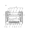
図1乃至図5を用いて、本実施形態に係るイメージセンサモジュール100の概略構成について詳細に説明する。図1は、本実施形態に係るイメージセンサモジュール100の概略構成を説明する断面図である。図2は、本実施形態に係るイメージセンサモジュール100の概略構成を説明する分解断面図である。図3は、本実施形態に係るイメージセンサモジュール100の概略構成を説明する断面図である。図1及び図2は、イメージセンサモジュール100の光軸を含む平面で切った断面を示している。図3は、図1のA−A´を通り、イメージセンサモジュール100の光軸に垂直な平面で切った断面を示している。
<First Embodiment>
[Schematic Configuration of Image Sensor Module 100]
A schematic configuration of the
本実施形態に係るイメージセンサモジュール100は、インターポーザ基板102と、イメージセンサ104と、レンズユニット106と、放熱部材134と、第3ケース136と、永久磁石140と、カバー138とを備えている。
The
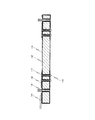
インターポーザ基板102は、第1面102a及び第2面102bを有している。第2面102bは、第1面102aとは反対側の面である。本実施形態に係るインターポーザ基板102の詳細な構成について、図面を用いて詳細に説明する。
The
図4は、本実施形態に係るインターポーザ基板102の構成を説明する斜視図である。図5は、本実施形態に係るインターポーザ基板102の構成を説明する平面図である。
FIG. 4 is a perspective view illustrating the configuration of the
インターポーザ基板102は、複数の貫通孔108を有する。複数の貫通孔108の各々は、その目的が異なるものを含み、本実施形態においては、その目的によって2種に分類される。以下の説明においては、それらを区別する場合には、第1貫通孔108A又は第2貫通孔108Bと呼称する。詳細は後述するが、複数の第1貫通孔108Aは、イメージセンサ104と外部回路(図示せず)とを電気的に接続するための電極をその内部に形成するために設けられる。一方、複数の第2貫通孔108Bは、レンズユニット106を第2面102b側に配置するための支柱118を、その内部に挿入するために設けられる。
The
本実施形態においては、複数の第1貫通孔108Aは、大まかに、矩形の4辺に沿って配置されている。矩形の対向する2つの長辺に沿って、それぞれ19個の第1貫通孔108Aが配置され、対向する2つの短辺に沿って、それぞれ11個の第1貫通孔Aが配置されている。矩形の各々の辺において、複数の第1貫通孔108Aは、2列に配置されている。更に、複数の第1貫通孔108Aは、ジグザグ状に配置されている。
In the present embodiment, the plurality of first through
尚、複数の第1貫通孔108Aの個数、レイアウト等については上述の構成に限られるものではない。第1貫通孔108Aの個数については、イメージセンサモジュール100と外部回路とを接続する配線を形成するために必要な個数以上であればよい。平面視における複数の第1貫通孔108Aのレイアウトについては、イメージセンサ104の受光面104aに配置される複数の光電変換素子と重畳しなければよい。
Note that the number, layout, and the like of the plurality of first through
一方、本実施形態においては、第2貫通孔108Bの数は4個である。4個の第2貫通孔108Bは、インターポーザ基板102の四隅近傍に配置されている。また、第2貫通孔109Bの径は、第1貫通孔108Aの径よりも大きい態様を示している。
On the other hand, in the present embodiment, the number of second through
尚、複数の第2貫通孔108Bの個数、レイアウト、径等については以上の構成に限られるものではない。第2貫通孔108Bの数については、詳細は後述するが、第2貫通孔108Bの数は3個以上であれば足りる。平面視における複数の第2貫通孔108Bのレイアウトについては、1本の直線上に配置されず、イメージセンサ104の受光面104aに配置される複数の光電変換素子と重畳しなければよい。第2貫通孔108Bの径については、支柱118を挿入するために十分な径であればよい。支柱118は、レンズユニット106をインターポーザ基板102の第2面102bに安定して配置するために十分な強度を有することが必要であることから、そのために十分な径が必要である。
The number, layout, diameter, and the like of the plurality of second through
インターポーザ基板102としては、その下方に配置されるイメージセンサ104の受光面104aに、被写体で反射した光を入射させるため、透光性を有する基板が用いられる。
As the
また、インターポーザ基板102の両表面は、レンズユニット106及びイメージセンサ104といった光学系の組み立て基準面を兼ねる。ここで、イメージセンサ104の受光面104aの法線と、レンズユニット106に配置された撮像レンズ群120の光軸とを高精度で一致させることが好ましい。そのため、インターポーザ基板102としては、両表面の平坦性が高く、かつ、両表面の平行度が高い基板を用いることが望ましい。
Further, both surfaces of the
そのような基板としては、例えばガラス基板を用いることができる。ガラス基板としては、例えば、石英ガラス、無アルカリガラス、ホウケイ酸ガラス、アルミノシリケートガラス、ソーダガラス、チタン含有シリケートガラス等を用いることができる。他の基板の例として、サファイア基板、炭化シリコン(SiC)基板、アルミナ(Al2O3)基板、窒化アルミ(AlN)基板、酸化ジリコニア(ZrO2)基板等を用いることができる。また、これらの基板のうちのいずれかの組み合わせで積層された基板を用いることができる。 As such a substrate, for example, a glass substrate can be used. As the glass substrate, for example, quartz glass, alkali-free glass, borosilicate glass, aluminosilicate glass, soda glass, titanium-containing silicate glass, or the like can be used. As examples of other substrates, a sapphire substrate, a silicon carbide (SiC) substrate, an alumina (Al 2 O 3 ) substrate, an aluminum nitride (AlN) substrate, a zirconia oxide (ZrO 2 ) substrate, or the like can be used. Moreover, the board | substrate laminated | stacked in any combination of these board | substrates can be used.
イメージセンサ104は、インターポーザ基板102の第1面102aに対向する位置に配置される。イメージセンサ104は、複数の第1貫通孔108A中の電極を介して、外部回路(図示せず)に接続される。イメージセンサ104は、インターポーザ基板102側に受光面104aを有している。受光面104aには、複数の光電変換素子が、例えば行列状に配置される。光電変換素子としては、例えば、CMOSイメージセンサ、CCDイメージセンサ等を用いることができる。
The
本実施形態においては、光電変換素子として、COMSイメージセンサを用いる。図6は、本実施形態に係るCMOSイメージセンサの構成を説明する断面図である。 In the present embodiment, a COMS image sensor is used as the photoelectric conversion element. FIG. 6 is a cross-sectional view illustrating the configuration of the CMOS image sensor according to the present embodiment.
本実施形態に係るCMOSイメージセンサは、フォトダイオード148、配線層150、カラーフィルタ152、及びマイクロレンズ154を有している。
The CMOS image sensor according to this embodiment includes a
フォトダイオード148は、入射した光を電荷に変換する。フォトダイオード148に光が入射すると、その一部がフォトダイオード148のPN接合部近傍で電子・正孔対を生成する。このとき、フォトダイオード148に逆バイアスを印加しておくことによって、生成されたキャリア対の情報を電流として取り出すことができる。
The
配線層150は、本実施形態においては、フォトダイオード148の上の層に配置される。配線層150は、フォトダイオード148内で生成されたキャリア対の信号を検出するための配線及びトランジスタ等の素子を有している。これらの配線や素子等は、フォトダイオード148に効率的に外光を取り込むため、フォトダイオード148の上部を避けて配置されている。
In the present embodiment, the
カラーフィルタ152は、フォトダイオード148に入射する光の色を選択する。複数のCMOSイメージセンサの各々は、少なくとも3色のいずれかのカラーフィルタ152を有している。
The
マイクロレンズ154は、入射した光をフォトダイオード148に効率良く集光するために設けられる。集光の効率を向上させるため、マイクロレンズ154の下には、平坦化層156を設けてもよい。
The
以上、本実施形態に係るイメージセンサ104の受光面104aに配置されたCMOSイメージセンサ104について説明した。
The
レンズユニット106は、インターポーザ基板102の第2面102bに対向する位置に配置される。レンズユニット106は、撮像レンズ群120、第1ケース122、第2ケース124、複数の支柱118、及び赤外線フィルタ128を有している。
The
撮像レンズ群120は、複数のレンズを含んでもよく、被写体が発してイメージセンサモジュール100に入射した光を、イメージセンサ104の受光面104a上に結像させる。
The
第1ケース122は、撮像レンズ群120を有する。本実施形態においては、第1ケース122は、撮像レンズ群120を内装している。第1ケース122は、円筒形の形状を有し、その側壁が、撮像レンズ群120が有する複数のレンズの周囲を支持している。また、第1ケース122には、コイル130が巻き付けられている。コイル130は、撮像レンズ群120の配置を制御するために設けられている。コイル130に供給する電流を制御することによって、当該電流が誘発する磁場と永久磁石140との相互作用により、撮像レンズ群120の配置を制御する。
The
第2ケース124は、第1ケース122と接合されている。本実施形態においては、第2ケース124は、複数のバネ132を介して第1ケース122と接合され、第1ケース122を内装している。これによって、第1ケース122は、コイル130に供給される電流を制御することによって、第2ケース124に対して揺動可能に配置される。第2ケース124は、本実施形態においては、四角柱状の形状を有している。第2ケース124の撮像レンズ群120に対向する側面には、外光をイメージセンサモジュール100内に取り込むために透明樹脂基板126が用いられている。
The
複数の支柱118は、第2ケース124に設けられている。複数の支柱118の各々は、インターポーザ基板102の複数の第2貫通孔108Bに挿入されている。これによって、レンズユニット106をインターポーザ基板102の第2面102bに着脱可能に配置することができる。
The plurality of
支柱118の本数は、レンズユニット106をインターポーザ基板102の第2面102bに安定して配置するため、3本以上であることが好ましい。平面視における複数の支柱118のレイアウトについては、1本の直線上に配置されず、イメージセンサ104の受光面104aに配置される複数の光電変換素子と重畳しなければよい。支柱118は、レンズユニット106をインターポーザ基板102の第2面102bに安定して配置するために十分な強度を有することが必要であることから、そのために十分な径が必要である。
The number of
複数の支柱118の内、2本の支柱118は、コイル130に接続されている。当該2本の支柱118は、コイル130の両端に接続されてもよい。当該2本の支柱を介してコイル130に供給する電流を制御することによって、撮像レンズ群120の位置を制御する。
Of the plurality of
このような構成を有することによって、支柱118がコイル130に接続される配線を兼ねることができ、配線構造が単純になる。
By having such a configuration, the
赤外線フィルタ128は、撮像レンズ群120を透過して入射する光から赤外領域の光を吸収するフィルタである。本実施形態においては、赤外線フィルタ128は、レンズユニット106内に配置され、撮像レンズ群120の下部に配置されている。しかし、赤外線フィルタ128の配置はこれに限定されない。つまり、被写体からの光が撮像レンズ群120を通過し、その後に赤外線フィルタ128を通過する構成となっていればよい。他の例として、インターポーザ基板102の第1面102a側に固定されて配置されていてもよい。
The
以上、本実施形態に係るイメージセンサモジュール100が備えるレンズユニット106の構成について説明した。このような構成を有することによって、本実施形態に係るイメージセンサモジュール100は、イメージセンサ104の受光面104aの法線と、レンズユニット106に配置された撮像レンズ群120の光軸とを高精度で一致させることができる。
The configuration of the
イメージセンサ104の受光面104aの法線と、撮像レンズ群120の光軸とが一致していないと、例えばイメージセンサ104の有効な受光面104aの中心部付近で被写体の像を良好に結像させたとしても、有効な受光面104aの中心部から離れた領域においては良好に結像させることができないといった表示不良の発生が懸念される。
If the normal line of the
放熱部材134は、イメージセンサ104の受光面104aとは反対の面に固定されて配置されている。
The
第3ケース136は、凹部を有し、当該凹部内に少なくともイメージセンサ104及び放熱部材134が配置され、インターポーザ基板102に固定されて配置されている。
The
永久磁石140は、第2ケース124の外側に、コイル130を囲むように配置されている。本実施形態においては、第2ケースの4個の側面の各々に、1個の永久磁石140が配置されている。尚、本実施形態の永久磁石140のレイアウトは一例であって、これに限られるものではない。
The
カバー138は、レンズユニット106及び永久磁石140を内装する。カバーの材質138としては、金属、セラミック等を用いることができる。
The
以上、本実施形態に係るイメージセンサモジュール100の概略構成について説明した。本実施形態に係るイメージセンサモジュール100の構成によれば、インターポーザ基板102は光学系の組み立て基準面を兼ねる。これによって、簡便かつ高精度な光学系の組み立てが可能になる。つまり、イメージセンサ104の受光面104aの法線と、レンズユニット106に配置された撮像レンズ群120の光軸とを簡便かつ高精度で一致させることができる。
The schematic configuration of the
[インターポーザ基板102周辺の構成]
次いで、本実施形態に係るイメージセンサモジュール100のインターポーザ基板102周辺の構成について詳細に説明する。図7は、本実施形態に係るイメージセンサモジュール100のインターポーザ基板102周辺の構成を説明する断面図である。
[Configuration around the interposer substrate 102]
Next, the configuration around the
本実施形態のように、イメージセンサモジュール100は、インターポーザ基板102の表面上の一部に、光吸収層112を有していてもよい。本実施形態おいては、インターポーザ基板102の表面上、インターポーザ基板102の側面上、及び複数の貫通孔108の側壁上、かつ、イメージセンサ104の受光面104a以外の領域に光吸収層112を有する。換言すると、光吸収層112は、被写体で反射した光をイメージセンサ104の受光面104aに入射させるために、イメージセンサ104の受光面104aを露出する開口部を有している。
As in this embodiment, the
光吸収層112は、インターポーザ基板102内に侵入した光が、電極等で乱反射して迷光となることを抑制するために設けられる。そのような迷光がイメージセンサ104に入射すると、フレアとなって撮影画像に現れることが懸念される。よって、光吸収層112の材料としては、インターポーザ基板102内に侵入した光を吸収し、それを透過及び反射させない材料であることが好ましい。
The light absorption layer 112 is provided in order to prevent light that has entered the
光吸収層112の材料としては、例えば、金属、黒色樹脂等を用いることができる。金属としては、例えばニッケル(Ni)、鉛(Pb)、金(Au)、銅(Cu)等を用いることができる。黒色樹脂としては、少なくとも、感光性樹脂組成物、光重合開始剤、顔料及び溶媒を含み、これらの組成を適宜合わせて黒色樹脂組成物とする。感光性樹脂組成物としては、ネガ型の感光性樹脂組成物を用いることができる。また、感光性樹脂組成物としては、例えばアクリル系モノマー、オリゴマー、ポリマーを含有する感光性樹脂組成物を用いることができる。顔料としては、カーボンブラック、酸化チタンや酸窒化チタン等のチタンブラック、酸化鉄等の金属酸化物、その他混色した有機顔料等を用いることができる。また、黒色樹脂としては、非感光性樹脂組成物に、顔料を分散させたものを用いることができる。非感光性樹脂組成物としては、例えばポリイミド樹脂を用いることができる。顔料としては、カーボンブラックを分散させたものを用いることができる。また、アニリンブラック、アセチレンブラック、フタロシアニンブラック、チタンブラック等を顔料として分散してもよい。 As a material of the light absorption layer 112, for example, metal, black resin, or the like can be used. As the metal, for example, nickel (Ni), lead (Pb), gold (Au), copper (Cu), or the like can be used. The black resin includes at least a photosensitive resin composition, a photopolymerization initiator, a pigment, and a solvent, and these compositions are appropriately combined to form a black resin composition. As the photosensitive resin composition, a negative photosensitive resin composition can be used. Moreover, as a photosensitive resin composition, the photosensitive resin composition containing an acryl-type monomer, an oligomer, and a polymer can be used, for example. Examples of the pigment include carbon black, titanium black such as titanium oxide and titanium oxynitride, metal oxide such as iron oxide, and other mixed organic pigments. Moreover, as a black resin, what disperse | distributed the pigment to the non-photosensitive resin composition can be used. As the non-photosensitive resin composition, for example, a polyimide resin can be used. A pigment in which carbon black is dispersed can be used as the pigment. Further, aniline black, acetylene black, phthalocyanine black, titanium black or the like may be dispersed as a pigment.
インターポーザ基板102が有する複数の第1貫通孔108Aの各々には、第1貫通電極110Aが設けられる。ここで、複数の第1貫通電極110A、インターポーザ基板102の両面に配置される配線142等の金属は、透光性を有するインターポーザ基板102に接して配置されることは無く、光吸収層112を介してインターポーザ基板102に配置される。
A first through electrode 110A is provided in each of the plurality of first through
第1貫通電極110Aは、本実施形態のように、第1貫通孔108Aを充填するように配置してもよい。また、詳細は後述するが、第1貫通電極110Aは、第1貫通孔108Aの側壁上のみに配置することによって中空としてもよい。更に、第1貫通電極110Aを第1貫通孔108Aの側壁上のみに配置することによって中空となった空間を、樹脂等の絶縁材料で充填してもよい。
110 A of 1st penetration electrodes may be arrange | positioned so that 108 A of 1st penetration holes may be filled like this embodiment. Although details will be described later, the first through electrode 110A may be hollow by being disposed only on the side wall of the first through
インターポーザ基板102が有する複数の第2貫通孔108Bの各々には、第2貫通電極110Bが設けられてもよい。しかし、これは必須ではない。第2貫通孔108Bには支柱118が挿入されるため、第2貫通電極110Bが設けられる場合は、第2貫通孔108Bの側壁上のみに配置することによって、中空とする。
A second through electrode 110B may be provided in each of the plurality of second through
インターポーザ基板102の両面において、イメージセンサ104に対向する領域に形成された反射防止層114を有していてもよい。反射防止層114としては、例えばモスアイ構造を有するシート等を用いることができる。
On both surfaces of the
このような構成を有することによって、インターポーザ基板102の表面における光の反射が抑制され、イメージセンサ104は効率的に受光することができる。
With such a configuration, reflection of light on the surface of the
本実施形態においては、複数の貫通電極110の、インターポーザ基板102の第1面102a側端部に配置された半田ボール116を介してイメージセンサ104が有する配線142と接続される。つまり、イメージセンサ104は、インターポーザ基板102に対してフリップチップ接続される。
In the present embodiment, the plurality of through
以上、本実施形態に係るイメージセンサモジュール100のインターポーザ基板102周辺の構成について説明した。このような構成を有することによって、インターポーザ基板102内に侵入した光の乱反射による迷光を抑制することができ、それに伴うフレアの発生を抑制することができる。光吸収層112を設けないと、インターポーザ基板102内に侵入した光が、貫通電極110や配線142等の金属によって乱反射して迷光となり、フレアが発生する懸念がある。
The configuration around the
[貫通孔、光吸収層及び貫通電極の形成方法]
インターポーザ基板102に対し、貫通孔108の形成から貫通電極110形成までの方法の一例について説明する。
[Method of forming through hole, light absorbing layer and through electrode]
An example of a method from the formation of the through
先ず、インターポーザ基板102に貫通孔108を形成する方法について説明する。貫通孔108を形成する方法としては、レーザ照射、ウェットエッチング、ドライエッチング等を用いることができる。
First, a method for forming the through
レーザ照射としては、エキシマレーザ、Nd:YAGレーザ(基本波(波長:1064nm)、第2高調波(波長:532nm)、第3高調波(波長:355nm)等を用いることができる。)、フェムト秒レーザ等を用いることができる。 As the laser irradiation, excimer laser, Nd: YAG laser (fundamental wave (wavelength: 1064 nm), second harmonic (wavelength: 532 nm), third harmonic (wavelength: 355 nm), etc.), femto can be used. A second laser or the like can be used.
ウェットエッチングとしては、フッ化水素(HF)、硫酸(H2SO4)、硝酸(HNO3)、塩酸(HCl)のいずれか、またはこれらのうちの混合物を用いたウェットエッチング等を用いることができる。また、前述のレーザ照射とウェットエッチングを適宜組み合わせることもできる。つまり、レーザ照射によってインターポーザ基板102の貫通孔形成領域に変質層を形成し、HFに浸漬することによって当該変質層をエッチングすることができる。
As wet etching, it is possible to use wet etching using hydrogen fluoride (HF), sulfuric acid (H 2 SO 4 ), nitric acid (HNO 3 ), hydrochloric acid (HCl), or a mixture thereof. it can. Further, the laser irradiation and wet etching described above can be combined as appropriate. That is, an altered layer can be formed in the through-hole formation region of the
ドライエッチングとしては、プラズマを用いたRIE(Reactive Ion Etching)法、ボッシュプロセスを用いたDRIE(Deep RIE)法、サンドブラスト法、レーザアブレーション等のレーザ加工等を用いることができる。 As dry etching, RIE (Reactive Ion Etching) using plasma, DRIE (Deep RIE) using Bosch process, sandblasting, laser processing such as laser ablation, or the like can be used.
以上、本実施形態に係るインターポーザ基板102の構成及び製造方法について説明した。次いで、光吸収層112を形成する方法について説明する。
The configuration and manufacturing method of the
先ず、前述の光吸収層112として用いることができる材料の内、金属を用いた光吸収層112を形成する方法について説明する。インターポーザ基板102において、前述のような光吸収層112が配置されない領域はレジストによって保護する。次いで、ダイシングによって各々のインターポーザ基板102に個片化する。次いで、個片化されたインターポーザ基板102について、無電解めっき法の前処理工程として、触媒を吸着させる。次いで、所定のめっき液に浸漬し、金属膜を形成する。次いで、レジスト剥離液に浸漬し、流水する。以上のような工程によって、遮光性を有する金属を用いた光吸収層112を形成することができる。
First, a method for forming the light absorption layer 112 using a metal among the materials that can be used as the light absorption layer 112 will be described. In the
次いで、前述の光吸収層112として用いることができる材料の内、黒色樹脂を用いた光吸収層112を形成する方法について説明する。インターポーザ基板102において、前述のような光吸収層112が配置されない領域はフィルムレジスト等の保護層を形成する。次いで、ダイシングによって各々のインターポーザ基板102に個片化する。次いで、個片化されたインターポーザ基板102について、黒色樹脂に浸漬し、黒色化させる。次いで、剥離液に浸漬し、保護層を除去する。以上のような工程によって、黒色樹脂を用いた光吸収層112を形成することができる。
Next, a method for forming the light absorption layer 112 using a black resin among the materials that can be used as the light absorption layer 112 will be described. In the
以上、光吸収層112を形成する方法について説明した。次いで、貫通電極110を形成する方法について説明する。
The method for forming the light absorption layer 112 has been described above. Next, a method for forming the through
貫通電極110を形成する方法としては、例えば、充填めっき、スパッタリング又は蒸着、コンフォーマルめっき等の方法を用いることができる。これらの方法を用いて形成された貫通電極110について、図8を用いて説明する。図8の上段に示された(a1)〜(d1)は、上記の方法によって形成された各々の貫通電極110の断面図であり、下段に示された(a2)〜(d2)は、各々の貫通電極110の上面図である。
As a method for forming the through
図8(a1)及び図8(a2)は、それぞれ、充填めっきによって形成された貫通電極110aの断面図及び上面図である。充填めっきは、貫通孔108の形成されたインターポーザ基板102の一方側からシード層である金属層を成膜し、電解めっき法により、当該金属層上にめっき層を成長させ、貫通孔108の一方の開口端を塞ぐ(蓋めっきを形成する)。そして、蓋めっきをシード層とした電解めっき法により、貫通孔108の内部を充填するめっき層を成長させる。
FIGS. 8A1 and 8A2 are a cross-sectional view and a top view, respectively, of the through
図8(b1)及び図8(b2)は、それぞれ、スパッタリング又は蒸着によって形成された貫通電極110bの断面図及び上面図である。図8(b1)及び図8(b2)に示す貫通電極110bは、貫通孔108の側壁に設けられており、貫通電極110bの内部には空洞が設けられている。スパッタリング又は蒸着によれば、貫通孔108の側壁に金属層を形成することができる。このとき、これらの処理をインターポーザ基板102の両面から施せば、片面のみの処理に比べて、アスペクト比の大きい貫通孔108に対しても貫通電極110を形成することが可能となる。また、無電解めっき法により、貫通孔108の側壁に金属層を形成することもできる。
FIGS. 8B1 and 8B2 are a cross-sectional view and a top view of the through
図8(c1)及び図8(c2)は、それぞれ、コンフォーマルめっきによって形成された貫通電極110cの断面図及び上面図である。図8(c1)及び図8(c2)に示す貫通電極110cは、上記の貫通電極110bと同様に貫通電極110cの内部に空洞が設けられている。コンフォーマルめっきは、前述のスパッタリング、蒸着又は無電解めっきによって貫通孔108の側壁に形成した金属層をシード層として、電解めっき法により、その上に内部に空洞が設けられためっき層を成長させる。
FIGS. 8C1 and 8C2 are a cross-sectional view and a top view, respectively, of the through
コンフォーマルめっきによって形成した貫通電極110cは、貫通孔108の内部が中空であるため、樹脂等を用いて貫通孔108を充填してもよい。図8(d1)及び図8(d2)は、それぞれ、コンフォーマルめっきによって形成された貫通電極110cに樹脂146を充填した貫通電極110dの断面図及び上面図である。
The through
以上、本実施形態に係るイメージセンサモジュール100について説明した。本実施形態に係るイメージセンサモジュール100には、イメージセンサ104及びレンズユニット106は、共にインターポーザ基板102を取り付け基準面として配置されている。
The
本実施形態に係るイメージセンサモジュール100は、以上のような構成を有することによって、イメージセンサ104の受光面104aの法線と、撮像レンズ群120の光軸とを簡便かつ高精度で一致させることができる。よって、イメージセンサ104の有効な受光面104a全域において被写体の像を均一に結像するよう制御することができる。
The
イメージセンサ104の受光面104aの法線と、撮像レンズ群120の光軸とが一致していないと、例えばイメージセンサ104の有効な受光面104aの中心部付近で被写体の像を良好に結像したとしても、有効な受光面104aの中心部から離れた領域においては良好に結像しないといった表示不良の発生が懸念される。
If the normal line of the
<第2実施形態>
図9及び図10を用いて、本実施形態に係るイメージセンサモジュール200の構成について詳細に説明する。図9は、本実施形態に係るイメージセンサモジュール200の構成を説明する断面図である。本実施形態に係るイメージセンサモジュール200は、第1実施形態に係るイメージセンサモジュール100と比較すると、インターポーザ基板102周辺の構成のみが異なっている。図10は、本実施形態に係るイメージセンサモジュール200のインターポーザ基板102周辺の構成を説明する断面図である。
Second Embodiment
The configuration of the
本実施形態に係るイメージセンサモジュール200は、複数の第1貫通孔108A中の第1貫通電極110Aの第1面102a側の端部が、第1面102aよりもイメージセンサ104側に位置する。換言すると、複数の第1貫通孔108A中の第1貫通電極110Aの第1面102a側の端部が、インターポーザ基板102から突出している。
In the
図10に示した破線Pは、インターポーザ基板102の第2面102bと平行な平面を示している。複数の第1貫通電極110Aの第1面102a側の端部は、破線P上に位置している。つまり、複数の第1貫通電極110Aの第1面102a側の端部は、インターポーザ基板102の第2面102bと平行な平面上に位置している。
A broken line P shown in FIG. 10 indicates a plane parallel to the
つまり、インターポーザ基板102とイメージセンサ104とのフリップチップ接続において、両者は突出した複数の第1貫通電極110Aのみで接続され、インターポーザ基板102の第1面102aとイメージセンサ104とは接触しない。
That is, in the flip-chip connection between the
このような構成を有することによって、イメージセンサ104とインターポーザ基板102が高精度で平行に配置され、製造工程における両者の位置合わせが容易になる。
By having such a configuration, the
面同士による接続の場合、例えば接続の工程において、両者の間に空気層等が生じてしまうと位置合わせのための制御が困難になり、歩留まりが低下する懸念がある。 In the case of connection between surfaces, for example, in the connection process, if an air layer or the like is generated between the two, control for alignment becomes difficult, and there is a concern that the yield may be reduced.
本実施形態に係るイメージセンサモジュール200が有する貫通電極110の形成方法の一例について説明する。先ず、前述した方法を用いて、少なくとも貫通孔108及び109の側壁に光吸収層112を形成する。ここで、貫通電極110は、その端部が貫通孔108の開口端まで充填され、貫通電極110が形成されたインターポーザ基板102としては可能な限り平坦となるように形成することが望ましい。次いで、インターポーザ基板102の第1面102aのみについて、貫通電極110を保護し、インターポーザ基板102のみをエッチングによって薄化する。
An example of a method for forming the through
以上の工程によって、本実施形態に係るイメージセンサモジュール200が有する貫通電極110を形成することができる。これによって、インターポーザ基板102第1面102aの平坦性は劣化するものの、イメージセンサ104との接続に関わる複数の貫通電極110の端部が同一平面上に存在することは維持される。この方法によれば、フリップチップ接続に用いる半田ボール116を必要としない。更に、フォトマスク等を用いたパターニングを必要とせず、自己整合的に貫通電極110が形成されるために、製造工程が簡略化される。
Through the above steps, the through
<第3実施形態>
図11及び図12を用いて、本実施形態に係るイメージセンサモジュール300の構成について詳細に説明する。図11は、本実施形態に係るイメージセンサモジュール300の構成を説明する断面図である。本実施形態に係るイメージセンサモジュール300は、第2実施形態に係るイメージセンサモジュール200と比較すると、インターポーザ基板102部分の構成のみが異なっている。図12は、本実施形態に係るイメージセンサモジュール300のインターポーザ基板102部分を説明する断面図である。
<Third Embodiment>
The configuration of the
本実施形態に係るイメージセンサモジュール300は、インターポーザ基板102は、第1面102a側に、複数の第1貫通電極110Aの側壁を囲む凸部を有している点で、第2実施形態に係るイメージセンサモジュール200と相違している。
The
図12に示した破線Pは、インターポーザ基板102の第2面102bと平行な平面を示している。複数の第1貫通電極110Aの第1面102a側の端部は、破線P上に位置している。つまり、複数の第1貫通電極110Aの第1面102a側の端部は、インターポーザ基板102の第2面102bと平行な平面上に位置している。
A broken line P shown in FIG. 12 indicates a plane parallel to the
つまり、インターポーザ基板102とイメージセンサ104とのフリップチップ接続において、両者は複数の突出した貫通電極110のみを介して接続され、インターポーザ基板102の第1面102aとイメージセンサ104とは接触しない。
That is, in the flip-chip connection between the
このような構成を有することによって、イメージセンサ104とインターポーザ基板102が高精度で平行に配置され、製造工程における両者の位置合わせが容易になる。また、貫通電極110の側壁がインターポーザ基板102で保護されているため、貫通電極110が形成されたインターポーザ基板102の機械的強度が向上する。
By having such a configuration, the
面同士による接続の場合、例えば接続の工程において、両者の間に空気層等が生じてしまうと位置合わせのための制御が困難になり、歩留まりが低下する懸念がある。 In the case of connection between surfaces, for example, in the connection process, if an air layer or the like is generated between the two, control for alignment becomes difficult, and there is a concern that the yield may be reduced.
本実施形態に係るイメージセンサモジュール300が有する貫通電極110の形成方法の一例について説明する。先ず、前述した方法を用いて、少なくとも貫通孔108及び109の側壁に光吸収層112を形成する。ここで、貫通電極110は、その端部が貫通孔108の開口端まで充填され、貫通電極110が形成されたインターポーザ基板102としては可能な限り平坦となるように形成することが望ましい。次いで、インターポーザ基板102の第1面102aのみについて、貫通電極110及びその周辺部を保護するレジストを形成し、エッチングによって薄化する。
An example of a method for forming the through
以上の工程によって、本実施形態に係るイメージセンサモジュール300が有する貫通電極110を形成することができる。これによって、インターポーザ基板102の第1面102aの平坦性は劣化するものの、イメージセンサ104との接続に関わる複数の貫通電極110の端部が同一平面上に存在することは維持される。貫通孔108の周辺領域で、エッチングされずに保護されたインターポーザ基板102の領域も、同一平面上に存在する。この方法によれば、フリップチップ接続に用いる半田ボール116を必要としない。また、貫通電極110の側壁がインターポーザ基板102で保護されているため、貫通電極110が形成されたインターポーザ基板102の機械的強度が向上する。
Through the above steps, the through
<他の実施形態>
図13及び図14は、本開示の実施形態に係るイメージセンサモジュールが搭載されることができる応用製品の例を示す図である。上記のように製造されたイメージセンサモジュール100乃至300は、様々な応用製品に搭載されることができる。例えば、ノート型パーソナルコンピュータ1000、タブレット端末2000、携帯電話3000、スマートフォン4000、デジタルビデオカメラ5000、デジタルカメラ6000等に搭載される。また、本開示の実施形態に係るイメージセンサモジュール300a及び300bが2個搭載されたデュアルカメラを有するスマートフォン4100等にも適用することができる。この例では、スマートフォン4100の背面にデュアルカメラが備えられた態様を示している。従来のような、一つの撮像素子のみから成るスマートフォンに搭載されるカメラは、撮像素子のサイズの制約に起因して被写界深度が非常に深くなってしまうという課題があった。そこで、二つの撮像素子を有するデュアルカメラをスマートフォンに搭載することによって、異なる二つの条件で画像を記録して撮影後に合成し、例えば一眼レフカメラと同等の被写界深度の調整が可能になる。更に、イメージセンサモジュール300a及び300bは2個に限られず、3個以上搭載されてもよい。ここで、複数のイメージセンサモジュールは、図示のスマートフォン4100のような横方向に一列に並べられた態様に限らず、縦方向に並べられてもよく、不規則な配置であってもよい。また、複数のイメージセンサモジュールの間隔に制限は無く、スマートフォンの両サイド近傍に配置されてもよく、対角近傍に配置されてもよい。更に、本開示の実施形態に係るイメージセンサモジュール300は、腕時計にも搭載されてもよい。腕時計7000は、竜頭7010の近傍にイメージセンサモジュール300が搭載される態様を示している。腕時計7100は、バンドの近傍(12時の方向)にイメージセンサモジュール300が搭載される態様を示している。腕時計7200は、表示パネルにイメージセンサモジュール300が搭載される態様を示している。そして、腕時計7300のように、腕時計7000の配置と反対の側面、つまり竜頭7010が配置された側面と反対側の側面にイメージセンサモジュール300が搭載されてもよい。
<Other embodiments>
13 and 14 are diagrams illustrating examples of application products in which the image sensor module according to the embodiment of the present disclosure can be mounted. The
なお、本開示は上記の実施形態に限られたものではなく、趣旨を逸脱しない範囲で適宜変更することが可能である。 Note that the present disclosure is not limited to the above-described embodiment, and can be changed as appropriate without departing from the spirit of the present disclosure.
100、200、300:イメージセンサモジュール 102:インターポーザ基板 102a:第1面 102b:第2面 104:イメージセンサ 104a:受光面 106:レンズユニット 108:貫通孔 108A:第1貫通孔 108B:第2貫通孔 110:貫通電極 110A:第1貫通電極 110B:第2貫通電極 112:光吸収層 114:反射防止層 116:半田ボール 117:凸部 118:支柱 120:撮像レンズ群 122:第1ケース 124:第2ケース 126:透明樹脂基板 128:赤外線フィルタ 130:コイル 132:バネ 134:放熱部材 136:第3ケース 138:カバー 140:永久磁石 142:配線 144:FPC 146:樹脂 148:フォトダイオード 150:配線層 152:カラーフィルタ 154:マイクロレンズ 156:平坦化層 1000:ノート型パーソナルコンピュータ 2000:タブレット端末 3000:携帯電話 4000、4100:スマートフォン 5000:デジタルビデオカメラ 6000:デジタルカメラ 7000、7100、7200:腕時計 7010:竜頭
100, 200, 300: Image sensor module 102:
Claims (8)
前記インターポーザ基板の前記第1面に対向する位置に配置されるイメージセンサであって、前記インターポーザ基板側に複数の光電変換素子が配置される受光面を有し、前記複数の貫通孔中の貫通電極を介して外部回路に接続されているイメージセンサと、
前記インターポーザ基板の前記第2面に対向する位置に配置されるレンズユニットと、
前記貫通孔の内壁と前記貫通電極との間に設けられた黒色樹脂の光吸収層と、を備え、
前記複数の貫通孔は、前記受光面を囲むように配置されているイメージセンサモジュール。 An interposer substrate having a first surface and a second surface opposite to the first surface, having translucency, and having a plurality of through holes;
An image sensor disposed at a position facing the first surface of the interposer substrate, having a light receiving surface on which a plurality of photoelectric conversion elements are disposed on the interposer substrate side, and penetrating through the plurality of through holes An image sensor connected to an external circuit via an electrode;
A lens unit disposed at a position facing the second surface of the interposer substrate;
A black resin light absorption layer provided between the inner wall of the through hole and the through electrode,
The plurality of through holes are image sensor modules arranged so as to surround the light receiving surface.
撮像レンズ群、
前記撮像レンズ群を有する第1ケース、
及び、複数のバネを介して前記第1ケースと接合されている第2ケースを含み、
前記第2ケースは、少なくとも3本の前記支柱を有する請求項2に記載のイメージセンサモジュール。 The lens unit is
Imaging lens group,
A first case having the imaging lens group;
And a second case joined to the first case via a plurality of springs,
The image sensor module according to claim 2 , wherein the second case has at least three of the support columns.
前記第1ケースを囲むコイル、
導電性を有し、前記コイルと接続されている少なくとも2本の前記支柱を有する請求項3に記載のイメージセンサモジュール。 The first case is
A coil surrounding the first case;
The image sensor module according to claim 3 , wherein the image sensor module has at least two pillars having conductivity and connected to the coil.
The image sensor module according to claim 7 , wherein the interposer substrate has a convex portion surrounding a side wall of the plurality of through electrodes on the second surface side.
Priority Applications (4)
| Application Number | Priority Date | Filing Date | Title |
|---|---|---|---|
| PCT/JP2016/072521 WO2017026317A1 (en) | 2015-08-10 | 2016-08-01 | Image sensor module |
| CN201680047033.9A CN107924924B (en) | 2015-08-10 | 2016-08-01 | Image sensor module |
| US15/892,464 US10681256B2 (en) | 2015-08-10 | 2018-02-09 | Image sensor module including a light-transmissive interposer substrate having a through-hole |
| US16/861,342 US11153471B2 (en) | 2015-08-10 | 2020-04-29 | Through-hole electrode substrate |
Applications Claiming Priority (2)
| Application Number | Priority Date | Filing Date | Title |
|---|---|---|---|
| JP2015158164 | 2015-08-10 | ||
| JP2015158164 | 2015-08-10 |
Related Child Applications (1)
| Application Number | Title | Priority Date | Filing Date |
|---|---|---|---|
| JP2017153487A Division JP6406404B2 (en) | 2015-08-10 | 2017-08-08 | Image sensor module |
Publications (3)
| Publication Number | Publication Date |
|---|---|
| JP2017038040A JP2017038040A (en) | 2017-02-16 |
| JP2017038040A5 JP2017038040A5 (en) | 2017-04-06 |
| JP6191728B2 true JP6191728B2 (en) | 2017-09-06 |
Family
ID=58047902
Family Applications (4)
| Application Number | Title | Priority Date | Filing Date |
|---|---|---|---|
| JP2016101074A Active JP6191728B2 (en) | 2015-08-10 | 2016-05-20 | Image sensor module |
| JP2017153487A Active JP6406404B2 (en) | 2015-08-10 | 2017-08-08 | Image sensor module |
| JP2018174906A Active JP6787378B2 (en) | 2015-08-10 | 2018-09-19 | Interposer board |
| JP2020179686A Active JP7095723B2 (en) | 2015-08-10 | 2020-10-27 | Interposer board |
Family Applications After (3)
| Application Number | Title | Priority Date | Filing Date |
|---|---|---|---|
| JP2017153487A Active JP6406404B2 (en) | 2015-08-10 | 2017-08-08 | Image sensor module |
| JP2018174906A Active JP6787378B2 (en) | 2015-08-10 | 2018-09-19 | Interposer board |
| JP2020179686A Active JP7095723B2 (en) | 2015-08-10 | 2020-10-27 | Interposer board |
Country Status (3)
| Country | Link |
|---|---|
| US (2) | US10681256B2 (en) |
| JP (4) | JP6191728B2 (en) |
| CN (1) | CN107924924B (en) |
Families Citing this family (7)
| Publication number | Priority date | Publication date | Assignee | Title |
|---|---|---|---|---|
| JP6191728B2 (en) * | 2015-08-10 | 2017-09-06 | 大日本印刷株式会社 | Image sensor module |
| CN110175492B (en) * | 2018-07-20 | 2022-03-01 | 神盾股份有限公司 | Optical fingerprint sensing device |
| WO2020129185A1 (en) * | 2018-12-19 | 2020-06-25 | オリンパス株式会社 | Imaging device and method for manufacturing imaging device |
| JP2020113630A (en) * | 2019-01-10 | 2020-07-27 | ソニーセミコンダクタソリューションズ株式会社 | Solid-state imaging device and electronic apparatus |
| JP7266189B2 (en) * | 2019-01-31 | 2023-04-28 | パナソニックIpマネジメント株式会社 | camera module and vehicle |
| CN113568257A (en) * | 2020-04-10 | 2021-10-29 | 新思考电机有限公司 | Camera device and electronic apparatus |
| TWI746082B (en) * | 2020-07-24 | 2021-11-11 | 海華科技股份有限公司 | Portable electronic device and image-capturing module thereof |
Family Cites Families (47)
| Publication number | Priority date | Publication date | Assignee | Title |
|---|---|---|---|---|
| JP4186481B2 (en) | 2002-03-07 | 2008-11-26 | ソニー株式会社 | Solid-state image sensor module and method for manufacturing solid-state image sensor module |
| JP2004063786A (en) * | 2002-07-29 | 2004-02-26 | Fuji Photo Film Co Ltd | Solid-state image sensing device and its manufacturing method |
| JP2004079745A (en) * | 2002-08-16 | 2004-03-11 | Sony Corp | Interposer, manufacturing method therefor, electronic circuit device and manufacturing method therefor |
| JP4839084B2 (en) | 2003-12-18 | 2011-12-14 | パナソニック株式会社 | Solid-state imaging device |
| JP2005244116A (en) | 2004-02-27 | 2005-09-08 | Toshiba Corp | Manufacturing method for semiconductor device |
| JP3987521B2 (en) * | 2004-11-08 | 2007-10-10 | 新光電気工業株式会社 | Substrate manufacturing method |
| JP4486005B2 (en) | 2005-08-03 | 2010-06-23 | パナソニック株式会社 | Semiconductor imaging device and manufacturing method thereof |
| JP2007299929A (en) | 2006-04-28 | 2007-11-15 | Matsushita Electric Ind Co Ltd | Optical device, and optical device module employing it |
| JP2008041801A (en) * | 2006-08-03 | 2008-02-21 | Renesas Technology Corp | Semiconductor device |
| KR101070921B1 (en) * | 2006-10-19 | 2011-10-06 | 삼성테크윈 주식회사 | Chip package for image sensor and method of manufacturing the same |
| JP4859682B2 (en) * | 2007-01-17 | 2012-01-25 | パナソニック株式会社 | Solid-state imaging unit and solid-state imaging device using the same |
| JP2008191267A (en) * | 2007-02-01 | 2008-08-21 | Sony Corp | Image blur compensation apparatus, lens barrel and imaging apparatus |
| JP2009099591A (en) * | 2007-10-12 | 2009-05-07 | Toshiba Corp | Solid-state image sensor and method of manufacturing the same |
| JP5248084B2 (en) * | 2007-10-26 | 2013-07-31 | 新光電気工業株式会社 | Silicon interposer, package for semiconductor device using the same, and semiconductor device |
| KR20090048920A (en) * | 2007-11-12 | 2009-05-15 | 삼성전자주식회사 | Camera module and electronic apparatus including the same |
| JP2009267151A (en) * | 2008-04-25 | 2009-11-12 | Sanyo Electric Co Ltd | Semiconductor device, and manufacturing method thereof |
| JP2009283902A (en) * | 2008-04-25 | 2009-12-03 | Panasonic Corp | Optical device and electronic apparatus including the same |
| JP2010034668A (en) * | 2008-07-25 | 2010-02-12 | Sharp Corp | Solid-state imaging device and electronic apparatus equipped with the same |
| JP2010045082A (en) * | 2008-08-08 | 2010-02-25 | Sharp Corp | Display element/electronic element module and its manufacturing method, and electronic information equipment |
| JP5498684B2 (en) | 2008-11-07 | 2014-05-21 | ラピスセミコンダクタ株式会社 | Semiconductor module and manufacturing method thereof |
| JP2010165804A (en) * | 2009-01-14 | 2010-07-29 | Panasonic Corp | Semiconductor device, electronic apparatus using the same, and method of manufacturing semiconductor device |
| JP5375219B2 (en) * | 2009-03-11 | 2013-12-25 | 富士通セミコンダクター株式会社 | Imaging device |
| JP5515357B2 (en) * | 2009-03-26 | 2014-06-11 | 株式会社ニコン | Imaging device and imaging module using the same |
| JP2010252164A (en) * | 2009-04-17 | 2010-11-04 | Panasonic Corp | Solid-state image sensing device |
| JP5150566B2 (en) | 2009-06-22 | 2013-02-20 | 株式会社東芝 | Semiconductor device and camera module |
| TW201110174A (en) * | 2009-06-24 | 2011-03-16 | Fujikura Ltd | Sheet luminescent device and manufacturing method thereof |
| CN101998034B (en) * | 2009-08-21 | 2013-04-24 | 鸿富锦精密工业(深圳)有限公司 | Image sensing module and camera module |
| JP2011128140A (en) * | 2009-11-19 | 2011-06-30 | Dainippon Printing Co Ltd | Sensor device and method of manufacturing the same |
| JP5609085B2 (en) * | 2009-12-03 | 2014-10-22 | 新光電気工業株式会社 | Semiconductor device and manufacturing method of semiconductor device |
| KR101737478B1 (en) * | 2009-12-14 | 2017-05-19 | 엘지이노텍 주식회사 | Camera module and manufacturing method thereof |
| JP2011205068A (en) | 2010-03-01 | 2011-10-13 | Sanyo Electric Co Ltd | Semiconductor device and method of manufacturing the same |
| JP2011187754A (en) * | 2010-03-10 | 2011-09-22 | Toshiba Corp | Solid-state imaging device and method of manufacturing the same |
| JP5771898B2 (en) * | 2010-03-17 | 2015-09-02 | 株式会社ニコン | Image sensor and camera |
| JP2013118206A (en) * | 2010-03-25 | 2013-06-13 | Panasonic Corp | Semiconductor device and manufacturing method of the same |
| JP5450295B2 (en) * | 2010-07-05 | 2014-03-26 | オリンパス株式会社 | Imaging apparatus and manufacturing method of imaging apparatus |
| JP5682185B2 (en) | 2010-09-07 | 2015-03-11 | ソニー株式会社 | Semiconductor package, semiconductor package manufacturing method, and optical module |
| JP5221615B2 (en) | 2010-09-21 | 2013-06-26 | 株式会社東芝 | Imaging device and manufacturing method thereof |
| JP2012222546A (en) | 2011-04-07 | 2012-11-12 | Sony Corp | Solid-state imaging device, method for manufacturing the same, and electronic apparatus |
| JP2013041922A (en) * | 2011-08-12 | 2013-02-28 | Sumitomo Bakelite Co Ltd | Light receiving device |
| JP2013104746A (en) * | 2011-11-11 | 2013-05-30 | Ricoh Co Ltd | Laser radar device |
| JP2013153361A (en) * | 2012-01-26 | 2013-08-08 | Konica Minolta Inc | Camera module |
| JP5931594B2 (en) * | 2012-06-07 | 2016-06-08 | 太陽誘電株式会社 | Capacitor |
| JP6071283B2 (en) * | 2012-07-04 | 2017-02-01 | キヤノン株式会社 | Radiation detection apparatus and manufacturing method thereof |
| JP2014093632A (en) * | 2012-11-02 | 2014-05-19 | Konica Minolta Inc | Camera module manufacturing method, camera module, and portable terminal |
| JP2015068853A (en) * | 2013-09-26 | 2015-04-13 | ソニー株式会社 | Laminated body, imaging element package, imaging apparatus, and electronic apparatus |
| JP2017014303A (en) * | 2013-11-21 | 2017-01-19 | 旭硝子株式会社 | Curable composition, cured product, camera module, and method of manufacturing imaging apparatus |
| JP6191728B2 (en) * | 2015-08-10 | 2017-09-06 | 大日本印刷株式会社 | Image sensor module |
-
2016
- 2016-05-20 JP JP2016101074A patent/JP6191728B2/en active Active
- 2016-08-01 CN CN201680047033.9A patent/CN107924924B/en active Active
-
2017
- 2017-08-08 JP JP2017153487A patent/JP6406404B2/en active Active
-
2018
- 2018-02-09 US US15/892,464 patent/US10681256B2/en active Active
- 2018-09-19 JP JP2018174906A patent/JP6787378B2/en active Active
-
2020
- 2020-04-29 US US16/861,342 patent/US11153471B2/en active Active
- 2020-10-27 JP JP2020179686A patent/JP7095723B2/en active Active
Also Published As
| Publication number | Publication date |
|---|---|
| US11153471B2 (en) | 2021-10-19 |
| JP6787378B2 (en) | 2020-11-18 |
| JP2019009464A (en) | 2019-01-17 |
| US20180205858A1 (en) | 2018-07-19 |
| JP6406404B2 (en) | 2018-10-17 |
| CN107924924B (en) | 2022-12-06 |
| JP2017204891A (en) | 2017-11-16 |
| JP2017038040A (en) | 2017-02-16 |
| JP2021028979A (en) | 2021-02-25 |
| JP7095723B2 (en) | 2022-07-05 |
| CN107924924A (en) | 2018-04-17 |
| US10681256B2 (en) | 2020-06-09 |
| US20200259980A1 (en) | 2020-08-13 |
Similar Documents
| Publication | Publication Date | Title |
|---|---|---|
| JP6406404B2 (en) | Image sensor module | |
| KR101453158B1 (en) | Stepped package for image sensor and method of making same | |
| JP5078725B2 (en) | Semiconductor device | |
| TWI379411B (en) | Electronic assembly for image sensor device | |
| US20140070349A1 (en) | Low Profile Image Sensor Package And Method | |
| US20090122178A1 (en) | Camera module and electronic apparatus having the same | |
| JP2008130603A (en) | Wafer level package for image sensor and manufacturing method therefor | |
| JP5701532B2 (en) | Manufacturing method of imaging apparatus | |
| KR20140111985A (en) | Cover-free sensor module and method of making same | |
| JP2013141257A (en) | Cover for image sensor assembly with light absorbing layer | |
| JP2010045082A (en) | Display element/electronic element module and its manufacturing method, and electronic information equipment | |
| WO2017026317A1 (en) | Image sensor module | |
| US9111826B2 (en) | Image pickup device, image pickup module, and camera | |
| JP2006294720A (en) | Camera module | |
| JP5356980B2 (en) | Electronic element module and manufacturing method thereof, electronic element wafer module and manufacturing method thereof, and electronic information device | |
| JP2013125881A (en) | Method of manufacturing solid-state imaging device | |
| CN104078477A (en) | Low Profile Sensor Module And Method Of Making Same | |
| JP6821994B2 (en) | Image sensor module | |
| JP6672632B2 (en) | Image sensor module | |
| TWI434570B (en) | Solid-state photography device and electronic device | |
| JP7014244B2 (en) | Interposer board | |
| JP2011199036A (en) | Solid-state image pickup device and method of manufacturing the same | |
| JP2018067631A (en) | Image sensor module | |
| JP2013161873A (en) | Solid-state imaging device and camera module | |
| JP5965984B2 (en) | Imaging device |
Legal Events
| Date | Code | Title | Description |
|---|---|---|---|
| A521 | Request for written amendment filed |
Free format text: JAPANESE INTERMEDIATE CODE: A523 Effective date: 20170306 |
|
| A621 | Written request for application examination |
Free format text: JAPANESE INTERMEDIATE CODE: A621 Effective date: 20170306 |
|
| A871 | Explanation of circumstances concerning accelerated examination |
Free format text: JAPANESE INTERMEDIATE CODE: A871 Effective date: 20170306 |
|
| A975 | Report on accelerated examination |
Free format text: JAPANESE INTERMEDIATE CODE: A971005 Effective date: 20170331 |
|
| A131 | Notification of reasons for refusal |
Free format text: JAPANESE INTERMEDIATE CODE: A131 Effective date: 20170411 |
|
| A521 | Request for written amendment filed |
Free format text: JAPANESE INTERMEDIATE CODE: A523 Effective date: 20170510 |
|
| A131 | Notification of reasons for refusal |
Free format text: JAPANESE INTERMEDIATE CODE: A131 Effective date: 20170530 |
|
| A521 | Request for written amendment filed |
Free format text: JAPANESE INTERMEDIATE CODE: A523 Effective date: 20170619 |
|
| TRDD | Decision of grant or rejection written | ||
| A01 | Written decision to grant a patent or to grant a registration (utility model) |
Free format text: JAPANESE INTERMEDIATE CODE: A01 Effective date: 20170711 |
|
| A61 | First payment of annual fees (during grant procedure) |
Free format text: JAPANESE INTERMEDIATE CODE: A61 Effective date: 20170724 |
|
| R150 | Certificate of patent or registration of utility model |
Ref document number: 6191728 Country of ref document: JP Free format text: JAPANESE INTERMEDIATE CODE: R150 |