JP5609085B2 - Semiconductor device and manufacturing method of semiconductor device - Google Patents
Semiconductor device and manufacturing method of semiconductor device Download PDFInfo
- Publication number
- JP5609085B2 JP5609085B2 JP2009275861A JP2009275861A JP5609085B2 JP 5609085 B2 JP5609085 B2 JP 5609085B2 JP 2009275861 A JP2009275861 A JP 2009275861A JP 2009275861 A JP2009275861 A JP 2009275861A JP 5609085 B2 JP5609085 B2 JP 5609085B2
- Authority
- JP
- Japan
- Prior art keywords
- semiconductor device
- wiring layer
- columnar conductors
- substrate
- columnar
- Prior art date
- Legal status (The legal status is an assumption and is not a legal conclusion. Google has not performed a legal analysis and makes no representation as to the accuracy of the status listed.)
- Active
Links
Images


Classifications
-
- H—ELECTRICITY
- H01—ELECTRIC ELEMENTS
- H01L—SEMICONDUCTOR DEVICES NOT COVERED BY CLASS H10
- H01L2224/00—Indexing scheme for arrangements for connecting or disconnecting semiconductor or solid-state bodies and methods related thereto as covered by H01L24/00
- H01L2224/01—Means for bonding being attached to, or being formed on, the surface to be connected, e.g. chip-to-package, die-attach, "first-level" interconnects; Manufacturing methods related thereto
- H01L2224/10—Bump connectors; Manufacturing methods related thereto
- H01L2224/15—Structure, shape, material or disposition of the bump connectors after the connecting process
- H01L2224/16—Structure, shape, material or disposition of the bump connectors after the connecting process of an individual bump connector
- H01L2224/161—Disposition
- H01L2224/16151—Disposition the bump connector connecting between a semiconductor or solid-state body and an item not being a semiconductor or solid-state body, e.g. chip-to-substrate, chip-to-passive
- H01L2224/16221—Disposition the bump connector connecting between a semiconductor or solid-state body and an item not being a semiconductor or solid-state body, e.g. chip-to-substrate, chip-to-passive the body and the item being stacked
- H01L2224/16225—Disposition the bump connector connecting between a semiconductor or solid-state body and an item not being a semiconductor or solid-state body, e.g. chip-to-substrate, chip-to-passive the body and the item being stacked the item being non-metallic, e.g. insulating substrate with or without metallisation
-
- H—ELECTRICITY
- H01—ELECTRIC ELEMENTS
- H01L—SEMICONDUCTOR DEVICES NOT COVERED BY CLASS H10
- H01L2224/00—Indexing scheme for arrangements for connecting or disconnecting semiconductor or solid-state bodies and methods related thereto as covered by H01L24/00
- H01L2224/01—Means for bonding being attached to, or being formed on, the surface to be connected, e.g. chip-to-package, die-attach, "first-level" interconnects; Manufacturing methods related thereto
- H01L2224/26—Layer connectors, e.g. plate connectors, solder or adhesive layers; Manufacturing methods related thereto
- H01L2224/31—Structure, shape, material or disposition of the layer connectors after the connecting process
- H01L2224/32—Structure, shape, material or disposition of the layer connectors after the connecting process of an individual layer connector
- H01L2224/321—Disposition
- H01L2224/32151—Disposition the layer connector connecting between a semiconductor or solid-state body and an item not being a semiconductor or solid-state body, e.g. chip-to-substrate, chip-to-passive
- H01L2224/32221—Disposition the layer connector connecting between a semiconductor or solid-state body and an item not being a semiconductor or solid-state body, e.g. chip-to-substrate, chip-to-passive the body and the item being stacked
- H01L2224/32225—Disposition the layer connector connecting between a semiconductor or solid-state body and an item not being a semiconductor or solid-state body, e.g. chip-to-substrate, chip-to-passive the body and the item being stacked the item being non-metallic, e.g. insulating substrate with or without metallisation
-
- H—ELECTRICITY
- H01—ELECTRIC ELEMENTS
- H01L—SEMICONDUCTOR DEVICES NOT COVERED BY CLASS H10
- H01L2224/00—Indexing scheme for arrangements for connecting or disconnecting semiconductor or solid-state bodies and methods related thereto as covered by H01L24/00
- H01L2224/73—Means for bonding being of different types provided for in two or more of groups H01L2224/10, H01L2224/18, H01L2224/26, H01L2224/34, H01L2224/42, H01L2224/50, H01L2224/63, H01L2224/71
- H01L2224/732—Location after the connecting process
- H01L2224/73201—Location after the connecting process on the same surface
- H01L2224/73203—Bump and layer connectors
- H01L2224/73204—Bump and layer connectors the bump connector being embedded into the layer connector
-
- H—ELECTRICITY
- H01—ELECTRIC ELEMENTS
- H01L—SEMICONDUCTOR DEVICES NOT COVERED BY CLASS H10
- H01L25/00—Assemblies consisting of a plurality of individual semiconductor or other solid state devices ; Multistep manufacturing processes thereof
- H01L25/03—Assemblies consisting of a plurality of individual semiconductor or other solid state devices ; Multistep manufacturing processes thereof all the devices being of a type provided for in the same subgroup of groups H01L27/00 - H01L33/00, or in a single subclass of H10K, H10N, e.g. assemblies of rectifier diodes
- H01L25/04—Assemblies consisting of a plurality of individual semiconductor or other solid state devices ; Multistep manufacturing processes thereof all the devices being of a type provided for in the same subgroup of groups H01L27/00 - H01L33/00, or in a single subclass of H10K, H10N, e.g. assemblies of rectifier diodes the devices not having separate containers
- H01L25/065—Assemblies consisting of a plurality of individual semiconductor or other solid state devices ; Multistep manufacturing processes thereof all the devices being of a type provided for in the same subgroup of groups H01L27/00 - H01L33/00, or in a single subclass of H10K, H10N, e.g. assemblies of rectifier diodes the devices not having separate containers the devices being of a type provided for in group H01L27/00
- H01L25/0655—Assemblies consisting of a plurality of individual semiconductor or other solid state devices ; Multistep manufacturing processes thereof all the devices being of a type provided for in the same subgroup of groups H01L27/00 - H01L33/00, or in a single subclass of H10K, H10N, e.g. assemblies of rectifier diodes the devices not having separate containers the devices being of a type provided for in group H01L27/00 the devices being arranged next to each other
-
- H—ELECTRICITY
- H01—ELECTRIC ELEMENTS
- H01L—SEMICONDUCTOR DEVICES NOT COVERED BY CLASS H10
- H01L2924/00—Indexing scheme for arrangements or methods for connecting or disconnecting semiconductor or solid-state bodies as covered by H01L24/00
- H01L2924/15—Details of package parts other than the semiconductor or other solid state devices to be connected
- H01L2924/151—Die mounting substrate
- H01L2924/153—Connection portion
- H01L2924/1531—Connection portion the connection portion being formed only on the surface of the substrate opposite to the die mounting surface
-
- H—ELECTRICITY
- H01—ELECTRIC ELEMENTS
- H01L—SEMICONDUCTOR DEVICES NOT COVERED BY CLASS H10
- H01L2924/00—Indexing scheme for arrangements or methods for connecting or disconnecting semiconductor or solid-state bodies as covered by H01L24/00
- H01L2924/30—Technical effects
- H01L2924/35—Mechanical effects
- H01L2924/351—Thermal stress
- H01L2924/3511—Warping
Landscapes
- Internal Circuitry In Semiconductor Integrated Circuit Devices (AREA)
Description
本発明は、半導体装置およびその製造技術に関し、特に、有機基板上に搭載される半導体パッケージ(半導体装置)に適用して有効な技術に関する。 The present invention relates to a semiconductor device and a manufacturing technique thereof, and more particularly to a technique effective when applied to a semiconductor package (semiconductor device) mounted on an organic substrate.
特開2004−42082号公報(特許文献1)には、複数の半導体チップを搭載したマルチチップパッケージに関する技術が開示されている。このマルチチップパッケージでは、パッケージ基板(有機基板)上に載置されたシリコンインターポーザを介して複数の半導体チップが搭載されている。 Japanese Unexamined Patent Application Publication No. 2004-42082 (Patent Document 1) discloses a technique related to a multi-chip package in which a plurality of semiconductor chips are mounted. In this multichip package, a plurality of semiconductor chips are mounted via a silicon interposer mounted on a package substrate (organic substrate).
なお、本発明者は、発明した結果に基づき、先行技術調査を行った。その結果、特開2006−216723号公報(特許文献2)が抽出された。この特許文献2には、不要輻射ノイズを高い周波数帯域まで効果的に抑制することを目的として、対の平面電極間に空隙を有する領域を設け、その領域に柱状あるいは円柱状の複数の抵抗体を挟持させたプリント配線基板(有機基板)に関する技術が開示されている。 In addition, this inventor performed prior art search based on the result invented. As a result, JP 2006-216723 A (Patent Document 2) was extracted. In Patent Document 2, for the purpose of effectively suppressing unwanted radiation noise to a high frequency band, a region having a gap is provided between a pair of planar electrodes, and a plurality of columnar or columnar resistors are provided in the region. A technique related to a printed wiring board (organic substrate) sandwiched between layers is disclosed.
マルチチップパッケージ(半導体パッケージ)は、例えば、有機基板(例えばビルドアップ基板、プリント配線基板)上に複数の半導体チップ(以下、単にチップという)を搭載して構成された半導体装置である。このようなマルチチップパッケージは、例えばコンピュータなどの電子回路が構成された有機基材からなる基板(マザーボード)上に搭載される。 A multichip package (semiconductor package) is a semiconductor device configured by mounting a plurality of semiconductor chips (hereinafter simply referred to as chips) on, for example, an organic substrate (for example, a build-up substrate or a printed wiring board). Such a multichip package is mounted on a substrate (motherboard) made of an organic base material on which an electronic circuit such as a computer is configured.
ところで、有機基板を用いたマルチチップパッケージでは、シリコン(Si)を基材とするチップと有機基板との熱膨張係数のミスマッチにより、チップと有機基板との間に応力が発生して隙間が生じるなどにより、信頼性が低下する問題がある。また、例えば複数のチップ間を電気的に接続するための配線は、平坦性の乏しい有機基材に形成されるため、微細配線化に困難である。さらに、例えばチップ間の配線長が長くなることや、これにより有機基板自体が大型化してしまうことが考えられる。 By the way, in a multi-chip package using an organic substrate, stress is generated between the chip and the organic substrate due to a mismatch in thermal expansion coefficients between the silicon (Si) -based chip and the organic substrate, resulting in a gap. For example, there is a problem that reliability is lowered. In addition, for example, wiring for electrically connecting a plurality of chips is formed on an organic base material with poor flatness, so that it is difficult to make fine wiring. Further, for example, it is conceivable that the wiring length between chips becomes long, and that the organic substrate itself becomes large due to this.
このため、本発明者は、近年の半導体装置の小型化、高性能、高機能の要求に応えるべく、次世代パッケージに関する技術について検討している。図1に本発明者が検討している半導体装置100を模式的に示す。図1に示す半導体装置100は、シリコンインターポーザ110と、その上に搭載されたチップCP1、CP2とを含んで構成されており、半導体パッケージということもできる。なお、図1では、半導体装置100は、半導体装置100をキャビティによって収納するような放熱板120(例えば、ヒートスプレッダ)と共に有機基板130(例えば、マザーボード)上に搭載されている状態で示している。
For this reason, the present inventor is examining a technology relating to the next generation package in order to meet the recent demands for miniaturization, high performance, and high functionality of semiconductor devices. FIG. 1 schematically shows a
シリコンインターポーザ110はシリコンを基材111とするインターポーザであるため、同じシリコンを基材とするチップCP1、CP2との熱膨張係数のミスマッチがなくなる。このため、前述したような応力による問題が発生せず、半導体装置100の信頼性を向上することができる。また、シリコンインターポーザ110は基材111にシリコンを用いており、有機基板と比較して平坦化に優れているため、微細配線を形成し易い。
Since the
したがって、シリコンインターポーザ110を含む半導体装置100には、チップ間の配線長を短くし、微細配線によるバスラインの増加により、データ転送速度を向上することが期待できる。また、半導体装置100の高機能化において、シリコンインターポーザ110には、例えば、ロジック用の半導体素子が形成されたチップや、メモリ用の半導体素子が形成されたチップなどの異種チップを搭載することも期待できる。
Therefore, the
しかしながら、例えばマザーボードなどの有機基板130上に搭載された半導体装置100では、有機基板130とシリコンインターポーザ110との間で熱膨張係数のミスマッチにより、その間に応力が発生している。このため、例えば温度サイクル試験などの過負荷条件では、その応力によって、有機基板130とシリコンインターポーザ110とが互いに反って接合性が低下するなど、半導体装置100の信頼性が低下してしまう。特に、シリコンインターポーザ110上にチップCP1、CP2を含む複数のチップを搭載するような場合では、搭載する領域も拡大するため、シリコンインターポーザ110のサイズが例えば20mm角以上となると信頼性の低下は顕著になる。
However, in the
また、図1では、半導体装置100の放熱性を向上するために、チップCP1、CP2に対して共通の放熱板120を取り付け、チップCP1、CP2を冷却するようにしている。なお、チップCP1、CP2と放熱板120とは接合部材121を介して接合されており、放熱板120と有機基板130とは接合部材122を介して接合されている。
Further, in FIG. 1, in order to improve the heat dissipation of the
ここで、例えば、チップCP1にはロジックなどの熱抵抗が大きく発熱量が高い半導体素子が形成され、チップCP2にはメモリなどの熱抵抗が小さく熱に弱い半導体素子が形成されている場合がある。このような場合では、放熱板120やシリコンインターポーザ110の基材111(シリコン)によって、チップCP1からの発熱は効率良く冷却されるが、その熱がチップCP2へ伝導してしまう。このため、チップCP2の温度が上昇することによって誤動作や熱破壊が起こる場合もあり、半導体装置100の信頼性が低下してしまう。
Here, for example, a semiconductor element having a large thermal resistance such as logic and a large amount of heat generated may be formed on the chip CP1, and a semiconductor element having a small thermal resistance such as a memory may be formed on the chip CP2. . In such a case, the heat generated from the chip CP1 is efficiently cooled by the
本発明の目的は、半導体装置の信頼性を向上することのできる技術を提供することにある。本発明の前記ならびにその他の目的と新規な特徴は、本明細書の記述および添付図面から明らかになるであろう。 An object of the present invention is to provide a technique capable of improving the reliability of a semiconductor device. The above and other objects and novel features of the present invention will be apparent from the description of this specification and the accompanying drawings.
なお、本発明者が先行技術調査によって抽出した特許文献2は、ノイズを抑制することを主題とするものであって、そのために空隙のあるパッケージが記載されているが、信頼性を向上するために、本願において開示される発明に関する記載はされていない。 In addition, patent document 2 which this inventor extracted by prior art search is a subject which suppresses noise, Comprising: The package with a space | gap is described for that purpose, In order to improve reliability No description is made regarding the invention disclosed in the present application.
本願において開示される発明のうち、代表的なものの概要を簡単に説明すれば、次のとおりである。本発明の一実施形態における半導体装置は、インターポーザと、前記インターポーザ上に設けられた半導体チップとを有する。前記インターポーザは、該インターポーザの厚さ方向に延在して互いに電気的に絶縁された複数の柱状導体と、前記半導体チップと前記複数の柱状導体との間に介在する、前記複数の柱状導体側の第1配線層、前記半導体チップ側の第2配線層、および前記第1配線層と前記第2配線層との間の絶縁層と、を有している。前記複数の柱状導体間には、外部に開放される空隙が設けられている。前記複数の柱状導体は、前記絶縁層から露出された前記第1配線層の表面と電気的に接続されている。前記半導体チップは、前記絶縁層から露出された前記第2配線層の表面と電気的に接続されている。前記空隙側における、前記複数の柱状導体と接続されずに前記絶縁層から露出された前記第1配線層の表面および前記複数の柱状導体のそれぞれの側面は、絶縁膜で覆われている。前記絶縁層から露出された前記第1配線層の表面には、前記絶縁膜を介して、前記第1配線層から延在する前記複数の柱状導体の根元を覆い、前記複数の柱状導体の立設を補強する第1補強材が設けられている。前記絶縁膜は、酸化シリコン膜からなる。前記第1補強材は、シリコン基板からなる。 Of the inventions disclosed in the present application, the outline of typical ones will be briefly described as follows. A semiconductor device according to an embodiment of the present invention includes an interposer and a semiconductor chip provided on the interposer. The interposer includes a plurality of columnar conductors extending in a thickness direction of the interposer and electrically insulated from each other, and the plurality of columnar conductors interposed between the semiconductor chip and the plurality of columnar conductors. A first wiring layer, a second wiring layer on the semiconductor chip side, and an insulating layer between the first wiring layer and the second wiring layer. Between the plurality of columnar conductors, gaps that are open to the outside are provided. The plurality of columnar conductors are electrically connected to the surface of the first wiring layer exposed from the insulating layer. The semiconductor chip is electrically connected to the surface of the second wiring layer exposed from the insulating layer. On the gap side, the surface of the first wiring layer exposed from the insulating layer without being connected to the plurality of columnar conductors and the side surfaces of the plurality of columnar conductors are covered with an insulating film. The surface of the first wiring layer exposed from the insulating layer covers the bases of the plurality of columnar conductors extending from the first wiring layer via the insulating film, and stands the standing of the plurality of columnar conductors. A first reinforcing material is provided to reinforce the installation. The insulating film is made of a silicon oxide film. The first reinforcing material is made of a silicon substrate.
本願において開示される発明のうち、代表的なものによって得られる効果を簡単に説明すると、前記一実施形態によって半導体装置の信頼性を向上することができる。 An effect obtained by a representative one of the inventions disclosed in the present application will be briefly described. The reliability of the semiconductor device can be improved by the one embodiment.
以下、本発明の実施形態を図面に基づいて詳細に説明する。なお、実施形態を説明するための全図において、同一の機能を有する部材には同一の符号を付し、その繰り返しの説明は省略する場合がある。 Hereinafter, embodiments of the present invention will be described in detail with reference to the drawings. Note that components having the same function are denoted by the same reference symbols throughout the drawings for describing the embodiments, and the repetitive description thereof may be omitted.
(実施形態1)
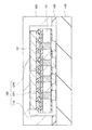
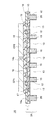
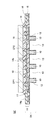
まず、本実施形態における半導体装置の構造について図2および図3を参照して説明する。図2は本実施形態における半導体装置1Aを模式的に示す断面図であり、図3は半導体装置1Aを模式的に示す平面図である。図2では図3のA−A線における半導体装置1Aの断面が示されている。また、図3では半導体装置1Aの裏面側からみた平面が示されており、裏面と反対面であるデバイス面に搭載されているチップCP1、CP2、CP3、CP4(破線で示す)が透視して示されている。また、図3では理解を容易にするために柱状導体10および枠体20にはハッチングを付している。
(Embodiment 1)
First, the structure of the semiconductor device according to the present embodiment will be described with reference to FIGS. FIG. 2 is a cross-sectional view schematically showing the
半導体装置1Aは、インターポーザ2Aと、インターポーザ2A上に設けられたチップCP1〜CP4とを有している。チップCP1は例えばCPUであり、チップCP1にはロジック用の半導体素子が形成されている。また、チップCP2〜CP4は例えばDRAMやフラッシュメモリであり、チップCP2〜CP4にはメモリ用の半導体素子が形成されている。これらチップCP1〜CP4を用いて、半導体装置1Aは所定の動作を行うことができる。
The
インターポーザ2Aは、その厚さ方向に延在して互いに電気的に絶縁された複数の柱状導体10と、チップCP1〜CP4と複数の柱状導体10とを介在する配線層11とを有している。複数の柱状導体10のそれぞれの側面は絶縁膜12で覆われており、複数の柱状導体10間に空隙13を有している。この空隙13はインターポーザ2A(半導体装置1A)の外部に開放されている。また、インターポーザ2Aは、複数の柱状導体10を囲む枠体20を外周に有している。
The
インターポーザ2Aの配線層11は、第1層(最下層)の配線層14aと、第2層(最上層)の配線層14bと、配線層14a、14b間の層間絶縁層15と、配線層14bの所望位置に形成された開口部を有するパッシベーション膜16とを含んで構成されている。例えば、配線層14a、14bは銅(Cu)を含んでなり、層間絶縁層15は酸化シリコンまたは有機樹脂を含んでなり、パッシベーション膜16は有機樹脂を含んでなる。このパッシベーション膜16は、インターポーザ2Aの表面保護膜となっており、最上層の配線層14bを保護している。一方、最下層の配線層14aは、柱状導体10の側面を覆う絶縁膜12が配線層14aに係るようにして形成され、例えば酸化シリコン膜などからなる絶縁膜12によって保護されている。なお、これらで構成される配線層11の全体での厚さは例えば15μm程度で形成される。
The
パッシベーション膜16の開口部から露出する配線層14bは、インターポーザ2Aの外部電極パッドとなっており、この外部電極パッドを介してチップCP1〜CP4と配線層11とは電気的に接続される。また、配線層11では、この外部電極パッドともなる配線層14bと、配線層14aとは、ビア(Via)17を介して相互に接続されている。また、配線層14a(配線層11)は、柱状導体10と電気的に接続されている。
The
このインターポーザ2A(配線層11)上に、チップCP1〜CP4が実装して設けられている。チップCP1〜CP4の主面(素子形成面)には、外部接続端子(図示しない)が形成されており、電極バンプ18を介して、インターポーザ2Aの電極パッド(配線層14b)にフリップチップ接続されている。また、チップCP1〜CP4とインターポーザ2A(配線層11)との間にはアンダーフィル樹脂19が充填されている。このアンダーフィル樹脂19によって、インターポーザ2AとチップCP1〜CP4の熱膨張係数のミスマッチを防止すると共に、インターポーザ2AとチップCP1〜CP4の接続性を向上させている。
On the
柱状導体10は、例えば、銅(Cu)を含む導体によって構成され、径が60μm程度、長さ(高さ)が300μm程度の円柱状で形成される。複数の柱状導体10は、配線層11から立設され、それらの間は外部に開放された空隙13となっている。このため、柱状導体10を露出した状態としたのでは、導体(例えば銅)が腐食して、電気的特性が劣化する場合がある。
The
そこで、本実施形態では、柱状導体10の側面に例えば酸化シリコン膜などの絶縁膜12を覆うことによって、柱状導体10が腐食するのを防止している。半導体装置1Aでは、空隙13が外部に開放された構造となっているので特に有効となる。柱状導体10の腐食の防止により、電気的特性の劣化を防止することによって、半導体装置1Aの信頼性を向上することができる。なお、柱状導体10の先端は、外部との電気的な接続を確保するため、側面の絶縁膜12のように覆われずに露出した状態としている。この状態であっても、接続後は例えばはんだなどによって保護されるので柱状導体10の先端は腐食しないこととなる。
Therefore, in this embodiment, the
同様に、空隙13側の配線層14aの表面も絶縁膜12で覆うことによって、配線層14aが腐食するのを防止している。この配線層14aの腐食の防止により、電気的特性の劣化を防止することによって、半導体装置1Aの信頼性を向上することができる。
Similarly, the surface of the
このような半導体装置1Aは、インターポーザ2A上に設けられたチップCP1〜CP4を含んで構成されており、半導体パッケージ(マルチチップパッケージ)である。半導体装置1Aは、例えば11mm角程度の大きさで形成されている。
Such a
ところで、図1を参照して説明した半導体装置100もチップCP1、CP2を含んで構成されているため、半導体パッケージである。この半導体装置100にはシリコンを基材すなわち支持体とするインターポーザ(シリコンインターポーザ110)上にチップCP1、CP2が設けられている。これに対して、半導体装置1Aのインターポーザ2Aには、このような基材(支持体)に対応するものがない。したがって、半導体装置1Aは基材レスパッケージということもでき、またインターポーザ2Aは配線層11がフィルム状(例えば、厚さが15μmで大きさが11mm角)となるためフレキシブル基板ともいえる。
Incidentally, the
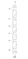
図4に半導体装置1Aを有機基板130(例えば、マザーボード)上に搭載した状態を示す。例えば、半導体装置1Aの複数の柱状導体10のそれぞれの先端に設けた例えば径が70μm程度のはんだボール21を介して、柱状導体10(例えば、銅)と有機基板130のパターン131(例えば、銅箔)とを接合して、半導体装置1Aが有機基板130上に搭載されている。このように半導体装置1Aは、複数の柱状導体10で接続する構造となっている。
FIG. 4 shows a state where the
半導体装置1Aは、配線層11から直立するように設けられた複数の柱状導体10を有しており、この複数の柱状導体10が脚となって有機基板130上に搭載されている。この複数の柱状導体10間は空隙13を有しているので、有機基板130とインターポーザ2Aとの間で生じる応力を緩和することができる。また、インターポーザ2Aの配線層11がフィルム状であるため、インターポーザ2AとチップCP1〜CP4との間で生じる応力も緩和することができる。このため、例えば温度サイクル試験などの過負荷条件においても、半導体装置1Aと有機基板130との間での反りが抑制され、半導体装置1Aとしての信頼性を向上することができる。
The semiconductor device 1 </ b> A has a plurality of
また、半導体装置1Aでは、複数のチップCP1〜CP4がインターポーザ2Aの配線層11側の同一面に混載されている。これらチップCP1〜CP4は、ロジック、メモリなどその機能やチップの大きさなどにより熱抵抗が異なる場合がある。例えば、インターポーザ2A上には、熱抵抗が高く発熱量が高いチップCP1(例えば、ロジック)と、熱抵抗が低く熱に弱いチップCP2〜CP4(例えば、メモリ)が搭載される場合がある。このような場合、発熱量が高いチップと、熱に弱いチップとで熱伝導を分離した構造とすることが有効である。
In the
そこで、半導体装置1A(インターポーザ2A)ではチップCP1〜CP4間には熱経路となる基板23の基材を設けないような空隙13を有する構造とし、例えばシリコンインターポーザを用いた場合の基材(シリコン)による熱伝導を、遮断している。シリコンは熱伝導率が非常に高く、発熱量の異なる複数のチップを搭載した場合、熱の移動による不具合が生じてしまう。したがって、発熱量が高いチップの影響により、熱に弱いチップの温度が上昇しすぎることによる誤動作や熱破壊が起きることを防止することができ、半導体装置1Aの信頼性を向上することができる。
Therefore, the
また、半導体装置1Aでは基材レスパッケージではあるが、単に基材がないのではなく、複数の柱状導体10を設け、その柱状導体10間に空隙13を有する構造となっている。このため空隙13を冷却路とし、その冷却路に空気や水などを流すことによって、放熱性を高めることもできる。これにより、発熱量が高いチップの影響により、熱に弱いチップの温度が上昇しすぎることによる誤動作や熱破壊が起きることをより防止することができ、半導体装置1Aの信頼性をより向上することができる。
Further, although the
また、複数の柱状導体10間に空隙13を有するので、柱状導体10間が例えばシリコンの場合よりもキャパシタンスを低減することができる。したがって、データ転送速度を向上することができる。
Further, since the
また、半導体装置1Aのインターポーザ2Aでは外周に枠体20を設けている。この枠体20の有無は適宜選択することができるが、本実施形態では、枠体20を設けた場合で説明している。
In addition, a
インターポーザ2Aは、複数の柱状導体10と配線層11とを有して構成されており、配線層11はフィルム状(例えば、厚さが15μm程度)となっているため、インターポーザ2Aをハンドリングすることが困難な場合も考えられる。そこで、インターポーザ2Aの外周に複数の柱状導体10を囲む枠体20を設けることによって、ハンドリング性を向上することができる。これにより、半導体装置1Aを有機基板130に容易に搭載することができる。
The
なお、半導体装置1Aの枠体20は有機基板130とは接合させずにフリーな状態であっても良いが、図4では、枠体20(例えば、銅)は接合部材22(例えば、はんだ)を介して有機基板130のパターン132(例えば、銅箔)と接合している。半導体装置1Aは、基材レスパッケージであるため、有機基板130に搭載後の実使用時において、外形(形態)の変形が問題となることも考えられる。そこで、枠体20を設け、その枠体20も有機基板130と接合することによって、半導体装置1Aの変形を防止している。
The
次に、本実施形態における半導体装置の製造方法について図面を参照して説明する。まず、図5に示すように、第1面23aとその反対面の第2面23bを有する所定の厚さの基板23を準備する。本実施形態では、基板23の基材をシリコンとしている。次いで、基板23の片面上にレジストを形成した後、フォトリソグラフィ技術を用いて、所望のパターン24を形成する。
Next, a method for manufacturing a semiconductor device in the present embodiment will be described with reference to the drawings. First, as shown in FIG. 5, a
続いて、パターン24をマスクとしたドライエッチングを用いて、図6に示すように、基板23の厚さ方向に延在する複数の貫通孔25と、貫通孔25を囲む貫通溝26を形成する。なお、図6では、貫通孔25、貫通溝26の形成後、パターン24が除去された状態である。また、後の製造工程で、貫通孔25に柱状導体10、貫通溝26に枠体20が形成されることとなる。
Subsequently, by using dry etching using the
この製造工程では、貫通溝26を形成することとしているが、貫通溝26の箇所を残すようにしても良い。後述するが、パターニングにより枠体20と類似した形状に基材(シリコン)を残すことで、シリコン枠体を形成しても良い。
In this manufacturing process, the through
続いて、図7に示すように、複数の貫通孔25の内壁に絶縁膜12を形成する。また、貫通溝26の内壁に絶縁膜12を形成する。具体的には、基板23としてシリコンを用いているので、基板23の表面を熱酸化することによって、酸化シリコン膜からなる絶縁膜12を形成することができる。
Subsequently, as shown in FIG. 7, the insulating
続いて、図8に示すように、複数の貫通孔25のそれぞれを導体(例えば、銅)で充填することによって、基板23の厚さ方向に延在して互いに電気的に絶縁された複数の柱状導体10を形成する。また、貫通溝26を導体(例えば、銅)で充填することによって、複数の柱状導体10を囲む枠体20を形成する。具体的には、基板23の第2面23bに導電板を貼り付け、その導電板をシードとした電解めっきにより貫通孔25、貫通溝26に導体(例えば、銅)を充填する。その後、基板23の第1面23a側で平坦処理し、また導電板を除去して、基板23の第2面23b側で平坦処理することによって、柱状導体10および貫通溝20が形成される。
Subsequently, as shown in FIG. 8, each of the plurality of through
続いて、図9に示すように、基板23の第1面23a上に複数の柱状導体10と電気的に接続される配線層11を形成する。例えば、セミアディティブ法によって、配線層14a、層間絶縁層15、および配線層14bが形成される。この配線層14bの形成の際には、配線層14aと配線層14bとを電気的に接続するビア17が形成される。また、配線層14b上にパッシベーション膜16がコーティング、パターニングされて配線層11が形成される。
Subsequently, as illustrated in FIG. 9, the
続いて、図10に示すように、配線層11上に配線層11と電気的に接続されるチップCP1〜CP4を搭載する。具体的には、チップCP1〜CP4の主面(素子形成面)に形成されている外部接続端子(図示せず)が、電極バンプ18を介して配線層14bにフリップチップ接続される。その後、チップCP1〜CP4と配線層11との間にはアンダーフィル樹脂19を充填する。
Subsequently, as shown in FIG. 10, chips CP <b> 1 to CP <b> 4 that are electrically connected to the
次いで、基板23においてチップCP1〜CP4が搭載されている第1面23aとは反対面の第2面23b側から、基板23の基材を除去する。具体的には、基板23の第2面23b側からドライエッチングすることによって、基材となっているシリコンを除去する。このとき、シリコン(基材)に対する銅(柱状導体10、枠体20)や酸化シリコン(絶縁膜12)の選択比によって、基材が除去され、柱状導体10、枠体20およびそれら側面の絶縁膜12は残存することとなる。
Next, the base material of the
このようにして、図2に示した半導体装置1A(基材レスパッケージ)が完成する。また、複数の柱状導体10と配線層11とを有するインターポーザ2Aも完成することとなる。
In this way, the
本実施形態では、配線層11上にチップCP1〜CP4を搭載した後、基板23の基材を除去して半導体装置1Aを完成させている。これに限らず、チップ搭載工程は適宜選択することができる。例えば、基板23の基材を除去した後、配線層11上にチップCP1〜CP4を搭載して半導体装置1Aを完成することもできる。
In this embodiment, after mounting the chips CP1 to CP4 on the
しかしながら、基板23の基材を除去することによって、配線層11はフィルム状となってしまうので、フィルム状の配線層11上にチップCP1〜CP4を搭載することは困難となる。そこで、本実施形態のように、チップCP1〜CP4を配線層11上に搭載することによって、これらチップCP1〜CP4を支持体として、基板23の基材を除去した方が、製造歩留まりを向上することができる。
However, since the
また、本実施形態では、インターポーザ2Aの枠体20を、柱状導体10と同一の製造工程で形成した場合について説明した。すなわち、図6を参照して説明した製造工程で貫通孔25と共に、貫通溝26を形成した後、図8を参照して説明した製造工程で貫通孔25に柱状導体10を形成すると共に、貫通溝26に枠体20を形成した。
Moreover, in this embodiment, the case where the
ここで、図6を参照して説明した製造工程で貫通孔25のみ形成し、貫通溝26を形成しない場合、例えば図9で示した状態では枠体20が形成されないこととなる。このような場合、基板23の第2面23bに、複数の柱状導体10を囲むようなレジストパターンを形成した後、図10を参照して説明したエッチング工程を行うことによって、枠体20と類似した形状の、基板23の基材(シリコン)からなる枠体を形成することができる。
Here, when only the through
また、インターポーザ2Aの枠体20がない場合、先にチップを搭載する方が有利となる。図17に、インターポーザ2Aにおいて枠体20がない場合のインターポーザ2A’と、それを有する半導体装置1A’を示す。このように枠体がない場合、インターポーザ2A’がフィルム状となってしまうので、このフィルム状態でチップCP1〜CP4を搭載することは困難となる。このため、枠体20を設けない場合、先にチップCP1〜CP4を搭載した後、基板23の基材を除去することが望ましい。
Further, when there is no
また、本実施形態では、図2に示したように、柱状導体10の先端は、外部との電気的な接続を確保するため、側面の絶縁膜12のように覆われずに露出した状態としている。柱状導体10の先端を露出させた場合の構造について図18および図19を参照して説明する。
Further, in this embodiment, as shown in FIG. 2, the end of the
図18では、例えば図2で示した柱状導体10側面の絶縁膜12が、先端側から一部後退した状態となっている。例えばはんだバンプなどの接合部材と接続する場合、柱状導体10の導体との接触面積が増加し、また濡れ性が絶縁膜12(例えば、酸化シリコン膜)より導体(例えば、銅)が良いため、接合部材の保持に有利となり、半導体装置の信頼性を向上させることができる。図18に示したような構造は、例えば、図10を参照して説明したエッチング工程で、エッチング強度を調整することで形成することができる。
In FIG. 18, for example, the insulating
一方、図19では、例えば図2で示した柱状導体10が、先端側から一部後退した状態となっている。例えばはんだバンプなどの接合部材と接続する場合、はんだと柱状導体10の導体との接触面積が減少するため、はんだバンプ(接合部材)の小径化に有利となる。例えば、半導体装置の小型化などに伴い、小径化されたはんだバンプを有する半導体装置の信頼性を向上することができる。図19に示したような構造は、例えば、図10で説明したエッチング工程後、柱状導体10(例えば、銅)をエッチングすること(例えば、塩化第二銅液を用いる)で形成することができる。
On the other hand, in FIG. 19, for example, the
(実施形態2)
本実施形態における半導体装置の構造について図11を参照して説明する。図11は本実施形態における半導体装置1Bを模式的に示す断面図である。なお、前記実施形態1で説明した半導体装置1Aでは、配線層14aの空隙13側に絶縁膜12を設けていたが、本実施形態では、補強材30を設けた点が相違する。よって、その点を中心に説明し、また、他の構造の説明は省略する場合がある。
(Embodiment 2)
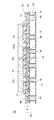
The structure of the semiconductor device in this embodiment will be described with reference to FIG. FIG. 11 is a cross-sectional view schematically showing the
半導体装置1Bのインターポーザ2Bでは、配線層11から延在する複数の柱状導体10の根元を覆い、複数の柱状導体10の立設を補強する補強材30が設けられている。この補強材30は、例えば絶縁性で、かつ、剛性を有するものであり、例えば、ガラス材からなる。このため、例えば、配線層11から柱状導体10が倒れるなどの不具合の発生を抑制することができるので、半導体装置1Bの信頼性を向上することができる。
In the interposer 2 </ b> B of the semiconductor device 1 </ b> B, a reinforcing
また、半導体装置1BではチップCP1〜CP4間には熱経路となる基板23の基材を設けないような空隙13を有する構造とし、例えばシリコンインターポーザを用いた場合の基材(シリコン)による熱伝導を、遮断している。したがって、発熱量が高いチップの影響により、熱に弱いチップの温度が上昇しすぎることによる誤動作や熱破壊が起きることを防止することができ、半導体装置1Bの信頼性を向上することができる。
Further, in the
また、配線層11の空隙13側に、補強材30を設けることによって、ハンドリング性を向上することができる。このため、図4を参照して説明した有機基板130に半導体装置1Bを容易に搭載することができる。
In addition, by providing the reinforcing
次に、本実施形態における半導体装置の製造方法について図面を参照して説明する。前記実施形態1において図6を参照して説明した製造工程後、図12に示すように、貫通孔25および貫通溝26を開口する開口部を有する補強材30を、基板23の第1面23aに形成する。具体的には、例えば、補強材30としてガラス板を用い、そのガラス板を基板23の第1面23aに接合した後、貫通孔25および貫通溝26に対応する開口部を、例えばエッチングによって除去する。
Next, a method for manufacturing a semiconductor device in the present embodiment will be described with reference to the drawings. After the manufacturing process described with reference to FIG. 6 in the first embodiment, as shown in FIG. 12, the reinforcing
あるいは、図5を参照して説明した製造工程において基板23を準備した後、基板23の第1面23aに補強材を形成する。その後、その補強材上に図5で示したようなパターン24を形成し、図6を参照して説明したエッチング工程によって、貫通孔25および貫通溝26と共に、貫通孔25および貫通溝26を開口する開口部を有する補強材30を形成しても良い。
Alternatively, after preparing the
その後は、前記実施形態1において図7〜図10を参照して説明した製造工程を経た後、図11に示した半導体装置1Bが完成する。また、複数の柱状導体10と配線層11とを有するインターポーザ2Bも完成することとなる。
Thereafter, after the manufacturing steps described with reference to FIGS. 7 to 10 in the first embodiment, the
(実施形態3)
本実施形態における半導体装置の構造について図13を参照して説明する。図13は本実施形態における半導体装置1Cを模式的に示す断面図である。なお、前記実施形態1で説明した半導体装置1Aでは、柱状導体10の側面(空隙13側)では絶縁膜12を設けていたが、本実施形態では、その絶縁膜12の外側(空隙13側)に補強材31を設けた点が相違する。よって、その点を中心に説明し、また、他の構造の説明は省略する場合がある。
(Embodiment 3)
The structure of the semiconductor device in this embodiment will be described with reference to FIG. FIG. 13 is a cross-sectional view schematically showing a
半導体装置1Cのインターポーザ2Cでは、複数の柱状導体10のそれぞれの側面には絶縁膜12を介して、複数の柱状導体10の立設を補強する補強材31が設けられている。この補強材31は、例えば剛性を有するものであり、例えば基板23の基材(例えばシリコン)からなる。このため、例えば、配線層11から柱状導体10が倒れるなどの不具合の発生を抑制することができるので、半導体装置1Cの信頼性を向上することができる。
In the interposer 2 </ b> C of the semiconductor device 1 </ b> C, a reinforcing
また、半導体装置1CではチップCP1〜CP4間には熱経路となる基板23の基材を設けないような空隙13を有する構造とし、例えばシリコンインターポーザを用いた場合の基材(シリコン)による熱伝導を、遮断している。したがって、発熱量が高いチップの影響により、熱に弱いチップの温度が上昇しすぎることによる誤動作や熱破壊が起きることを防止することができ、半導体装置1Cの信頼性を向上することができる。
Further, the
次に、本実施形態における半導体装置の製造方法について図面を参照して説明する。前記実施形態1において図8を参照して説明した製造工程後、図14に示すように、複数の柱状導体10の、基板23の第2面23b側端部のそれぞれに、柱状導体10の径より大きいパターン32を形成する。具体的には、例えば基板23の第2面23bに銅からなる層を形成した後、その銅層を異方性エッチングなどによってパターニングして、パターン32を形成する。これにより、パターン32は複数の柱状導体10の第2面23b側端部に設けられることとなる。
Next, a method for manufacturing a semiconductor device in the present embodiment will be described with reference to the drawings. After the manufacturing process described with reference to FIG. 8 in the first embodiment, as shown in FIG. 14, the diameter of the
その後は、前記実施形態1において図9〜図10を参照して説明した製造工程を経た後、図13に示した半導体装置1Cが完成する。また、複数の柱状導体10と配線層11とを有するインターポーザ2Cも完成することとなる。
Thereafter, after the manufacturing process described with reference to FIGS. 9 to 10 in the first embodiment, the
パターン32をマスクに基板23の基材を、図10を参照して説明したエッチングをすることによって、複数の柱状導体10のそれぞれの側面に絶縁膜12を介して、複数の柱状導体10の立設を補強する補強材31を形成することとなる。その後、パターン32を除去しても良いが、本実施形態では、パターン32を柱状導体10と同一の材料で形成しており、また柱状導体10の径よりも大きくしている。このため、外部接続端子として有効にパターン32を利用するため、パターン32を残存させている。
The base material of the
(実施形態4)
本実施形態における半導体装置の構造について図15を参照して説明する。図15は本実施形態における半導体装置1Dを模式的に示す断面図である。なお、前記実施形態1で説明した半導体装置1Aでは、複数の柱状導体10間のすべてに空隙13を形成していたが、本実施形態では、チップCP1〜CP4間で熱経路を遮断する空隙13を形成した点が相違する。よって、その点を中心に説明し、また、他の構造の説明は省略する場合がある。
(Embodiment 4)
The structure of the semiconductor device in this embodiment will be described with reference to FIG. FIG. 15 is a cross-sectional view schematically showing the
半導体装置1Dのインターポーザ2Dでは、基板23の基材がほとんど残存し、チップCP1〜CP4間で熱経路を遮断する位置にスリット状の空隙13が形成されている。なお、図3に示すような半導体装置1Dの平面では、チップCP1〜CP間の熱経路を遮断するように十字状のスリット(空隙13)が形成されることとなる。
In the
半導体装置1DではチップCP1〜CP4間には熱経路となる基板23の基材を設けないような空隙13を有する構造とし、例えばシリコンインターポーザを用いた場合の基材(シリコン)による熱伝導を、遮断している。したがって、発熱量が高いチップの影響により、熱に弱いチップの温度が上昇しすぎることによる誤動作や熱破壊が起きることを防止することができ、半導体装置1Dの信頼性を向上することができる。
In the
次に、本実施形態における半導体装置の製造方法について図面を参照して説明する。前記実施形態1において図9を参照して説明した製造工程後、図10に示すように、配線層11上に配線層11と電気的に接続されるチップCP1〜CP4を搭載し、チップCP1〜CP4と配線層11との間にはアンダーフィル樹脂19を充填する。
Next, a method for manufacturing a semiconductor device in the present embodiment will be described with reference to the drawings. After the manufacturing process described with reference to FIG. 9 in the first embodiment, chips CP1 to CP4 electrically connected to the
続いて、図16に示すように、基板23においてチップCP1〜CP4が搭載されている第1面23aとは反対面の第2面23b側から、複数の柱状導体10間にスリット(空隙13)を形成するように、基板23の基材を除去する。具体的には、ブレード33によってチップCP1〜CP4間で熱経路を遮断する位置にスリット(空隙13)を形成する。このようなスリットは、ブレード33を用いて形成する場合に限らず、エッチングなどを用いて形成しても良い。
Subsequently, as shown in FIG. 16, a slit (gap 13) is formed between the
これにより、図15に示した半導体装置1Dが完成する。また、複数の柱状導体10と配線層11とを有するインターポーザ2Dも完成することとなる。
Thereby, the
また、図11で示した補強材30のように、柱状導体10が倒れるなどの不具合を防止するために、基板23の基材(シリコン)でそのような補強材を構成しても良い。図20に、インターポーザ2Dにおいて、配線層11から延在する複数の柱状導体10の根元を覆うように基板23の一部を残存させた場合のインターポーザ2D’と、それを有する半導体装置1D’を示す。このように基板23の基材(シリコン)からなる補強材34を設けた場合にも、熱の移動を妨げるためスリット(空隙13)が必須となる。
Further, like the reinforcing
なお、インターポーザ2D’では、図16を参照して説明したスリット工程後、図10を参照して説明したエッチング工程が適用される。または、インターポーザ2D’では、図10を参照して説明したスリット工程後、図16を参照して説明したエッチング工程が適用される。
In the
以上、本発明者によってなされた発明を実施形態に基づき具体的に説明したが、本発明は前記実施形態に限定されるものではなく、その要旨を逸脱しない範囲で種々変更可能であることはいうまでもない。 As mentioned above, the invention made by the present inventor has been specifically described based on the embodiment. However, the present invention is not limited to the embodiment, and various modifications can be made without departing from the scope of the invention. Not too long.
例えば、熱抵抗が異なる複数の半導体チップを、前記実施形態ではインターポーザの同一面に搭載した場合について説明したが、インターポーザの上下両面に搭載しても良い。具体的には、熱抵抗の高い半導体チップをインターポーザの上面に搭載し、それよりも低い半導体チップをインターポーザの下面に搭載することもできる。これにより、熱抵抗が高く発熱量が高い半導体チップと、熱抵抗が低く熱に弱い半導体チップとを、インターポーザの厚さだけ離間できるので、冷却効果を高めることができる。 For example, although the case where a plurality of semiconductor chips having different thermal resistances are mounted on the same surface of the interposer has been described in the above embodiment, they may be mounted on both the upper and lower surfaces of the interposer. Specifically, a semiconductor chip having a high thermal resistance can be mounted on the upper surface of the interposer, and a semiconductor chip lower than that can be mounted on the lower surface of the interposer. Thereby, the semiconductor chip having a high thermal resistance and a high calorific value can be separated from the semiconductor chip having a low thermal resistance and weak against heat by the thickness of the interposer, so that the cooling effect can be enhanced.
1A、1A’、1B、1C、1D、1D’ 半導体装置
2A、2A’、2B、2C、2D、2D’ インターポーザ
10 柱状導体
11 配線層
12 絶縁膜
13 空隙
14a、14b 配線層
15 層間絶縁層
16 パッシベーション膜
17 ビア
18 電極バンプ
19 アンダーフィル樹脂
20 枠体
21 はんだボール
22 接合部材
23 基板
24 パターン
25 貫通孔
26 貫通溝
30、31 補強材
32 パターン
33 ブレード
34 補強材
100 半導体装置
110 シリコンインターポーザ
111 基材
120 放熱板
121、122 接合部材
130 有機基板
131、132 パターン
CP1、CP2、CP3、CP4 チップ
1A, 1A ′, 1B, 1C, 1D, 1D
Claims (9)
前記インターポーザは、
該インターポーザの厚さ方向に延在して互いに電気的に絶縁された複数の柱状導体と、
前記半導体チップと前記複数の柱状導体との間に介在する、前記複数の柱状導体側の第1配線層、前記半導体チップ側の第2配線層、および前記第1配線層と前記第2配線層との間の絶縁層と、
を有し、
前記複数の柱状導体間には、外部に開放される空隙が設けられ、
前記複数の柱状導体は、前記絶縁層から露出された前記第1配線層の表面と電気的に接続され、
前記半導体チップは、前記絶縁層から露出された前記第2配線層の表面と電気的に接続され、
前記空隙側における、前記複数の柱状導体と接続されずに前記絶縁層から露出された前記第1配線層の表面および前記複数の柱状導体のそれぞれの側面は、絶縁膜で覆われ、
前記絶縁層から露出された前記第1配線層の表面には、前記絶縁膜を介して、前記第1配線層から延在する前記複数の柱状導体の根元を覆い、前記複数の柱状導体の立設を補強する第1補強材が設けられ、
前記絶縁膜は、酸化シリコン膜からなり、
前記第1補強材は、シリコン基板からなることを特徴とする半導体装置。 A semiconductor device having an interposer and a semiconductor chip provided on the interposer,
The interposer is
A plurality of columnar conductors extending in the thickness direction of the interposer and electrically insulated from each other;
The first wiring layer on the side of the plurality of columnar conductors, the second wiring layer on the side of the semiconductor chip, and the first wiring layer and the second wiring layer interposed between the semiconductor chip and the plurality of columnar conductors An insulating layer between and
Have
Between the plurality of columnar conductors, a gap that is open to the outside is provided,
The plurality of columnar conductors are electrically connected to the surface of the first wiring layer exposed from the insulating layer,
The semiconductor chip is electrically connected to a surface of the second wiring layer exposed from the insulating layer;
On the gap side, the surface of the first wiring layer exposed from the insulating layer without being connected to the plurality of columnar conductors and the side surfaces of the plurality of columnar conductors are covered with an insulating film ,
The surface of the first wiring layer exposed from the insulating layer covers the bases of the plurality of columnar conductors extending from the first wiring layer via the insulating film, and stands the standing of the plurality of columnar conductors. A first reinforcing material is provided to reinforce the installation,
The insulating film is made of a silicon oxide film,
The semiconductor device according to claim 1, wherein the first reinforcing member is made of a silicon substrate .
前記複数の柱状導体のそれぞれの側面には、前記絶縁膜を介して、前記複数の柱状導体の立設を補強する第2補強材が設けられていることを特徴とする半導体装置。 The semiconductor device according to claim 1 ,
2. A semiconductor device according to claim 1, wherein a second reinforcing material for reinforcing standing of the plurality of columnar conductors is provided on each side surface of the plurality of columnar conductors via the insulating film.
前記半導体チップとして、発熱量の異なる第1および第2半導体チップが前記インターポーザ上に設けられ、
前記第1補強材の、平面視で前記第1および第2半導体チップの間に位置する箇所には、スリットが形成されていることを特徴とする半導体装置。 The semiconductor device according to claim 1 or 2 ,
As the semiconductor chip, first and second semiconductor chips having different heating values are provided on the interposer,
A semiconductor device, wherein a slit is formed at a location of the first reinforcing member located between the first and second semiconductor chips in plan view .
前記柱状導体の先端側の一部が、該柱状導体の側面を覆う前記絶縁膜から突出し、または後退していることを特徴とする半導体装置。 In the semiconductor device according to any one of claims 1 to 3 ,
A part of the front end side of the columnar conductor protrudes or recedes from the insulating film covering the side surface of the columnar conductor.
(b)前記複数の貫通孔の内壁を含む前記基板の表面全体に絶縁膜を形成する工程と、
(c)前記(b)工程後、前記複数の貫通孔のそれぞれを導体で充填することによって、前記基板の厚さ方向に延在して互いに電気的に絶縁された複数の柱状導体を形成する工程と、
(d)前記(c)工程後、前記基板の第1面上に前記複数の柱状導体と電気的に接続される第1配線層、前記第1配線層を覆う絶縁層、前記絶縁層上の第2配線層を形成する工程と、
(e)前記基板の第2面側から前記基板をエッチングすることによって、前記複数の柱状導体と接続されずに前記絶縁層から露出する前記第1配線層の表面および前記複数の柱状導体のそれぞれの側面を覆う前記絶縁膜を残存させて、前記複数の柱状導体間に空隙を形成する工程と、
(f)前記絶縁層から露出する前記第2配線層の表面に、半導体チップを電気的に接続して搭載する工程と、
を含むことを特徴とする半導体装置の製造方法。 (A) forming a plurality of through holes extending in the thickness direction in a substrate having a first surface and a second surface opposite to the first surface;
(B) forming an insulating film over the entire surface of the substrate including inner walls of the plurality of through holes;
(C) After the step (b), a plurality of columnar conductors extending in the thickness direction of the substrate and electrically insulated from each other are formed by filling each of the plurality of through holes with a conductor. Process,
(D) After the step (c), a first wiring layer electrically connected to the plurality of columnar conductors on the first surface of the substrate, an insulating layer covering the first wiring layer, and on the insulating layer Forming a second wiring layer;
(E) by etching the substrate from the second surface side of the substrate, the surface of the first wiring layer exposed from the insulating layer without being connected to the plurality of columnar conductors, and each of the plurality of columnar conductors Leaving the insulating film covering the side surfaces of the plurality of columnar conductors to form voids;
(F) a step of electrically connecting and mounting a semiconductor chip on the surface of the second wiring layer exposed from the insulating layer;
A method for manufacturing a semiconductor device, comprising:
前記(a)工程で前記複数の貫通孔を囲む貫通溝を形成した後、前記(c)工程で前記貫通溝を導体で充填すること、または、
前記(d)工程後、前記基板の第2面にレジストパターンを形成した後、前記(e)工程で前記基板をエッチングすること、
によって前記複数の柱状導体を囲む枠体を形成することを特徴とする半導体装置の製造方法。 In the manufacturing method of the semiconductor device according to claim 5 ,
After forming the through groove surrounding the plurality of through holes in the step (a), filling the through groove with a conductor in the step (c), or
After the step (d), a resist pattern is formed on the second surface of the substrate, and then the substrate is etched in the step (e).
A method of manufacturing a semiconductor device, comprising: forming a frame surrounding the plurality of columnar conductors.
前記(e)工程では、前記第1配線層から延在する前記複数の柱状導体の根元を覆うように前記基板を残存させてエッチングすることを特徴とする半導体装置の製造方法。 In the manufacturing method of the semiconductor device according to claim 5 or 6 ,
In the step (e), the semiconductor device is etched while leaving the substrate so as to cover the bases of the plurality of columnar conductors extending from the first wiring layer.
前記(d)工程後、前記(e)工程前に、前記複数の柱状導体の、前記基板の第2面側端部のそれぞれに、前記柱状導体の径より大きいパターンを形成し、
前記(e)工程では、前記パターンをマスクに前記基板をエッチングすることによって、前記複数の柱状導体のそれぞれの側面に前記絶縁膜を介して、前記複数の柱状導体の立設を補強する補強材を形成することを特徴とする半導体装置の製造方法。 In the manufacturing method of the semiconductor device according to claim 5 or 6 ,
After the step (d), before the step (e), a pattern larger than the diameter of the columnar conductor is formed on each of the second surface side ends of the plurality of columnar conductors,
In the step (e), a reinforcing material that reinforces the standing of the plurality of columnar conductors via the insulating film on each side surface of the plurality of columnar conductors by etching the substrate using the pattern as a mask. Forming a semiconductor device.
前記(e)工程では、前記複数の柱状導体間にスリットを形成するように、前記基板を除去することを特徴とする半導体装置の製造方法。 In the manufacturing method of the semiconductor device according to claim 5 or 6 ,
In the step (e), the substrate is removed so that a slit is formed between the plurality of columnar conductors.
Priority Applications (1)
| Application Number | Priority Date | Filing Date | Title |
|---|---|---|---|
| JP2009275861A JP5609085B2 (en) | 2009-12-03 | 2009-12-03 | Semiconductor device and manufacturing method of semiconductor device |
Applications Claiming Priority (1)
| Application Number | Priority Date | Filing Date | Title |
|---|---|---|---|
| JP2009275861A JP5609085B2 (en) | 2009-12-03 | 2009-12-03 | Semiconductor device and manufacturing method of semiconductor device |
Publications (3)
| Publication Number | Publication Date |
|---|---|
| JP2011119481A JP2011119481A (en) | 2011-06-16 |
| JP2011119481A5 JP2011119481A5 (en) | 2012-12-13 |
| JP5609085B2 true JP5609085B2 (en) | 2014-10-22 |
Family
ID=44284464
Family Applications (1)
| Application Number | Title | Priority Date | Filing Date |
|---|---|---|---|
| JP2009275861A Active JP5609085B2 (en) | 2009-12-03 | 2009-12-03 | Semiconductor device and manufacturing method of semiconductor device |
Country Status (1)
| Country | Link |
|---|---|
| JP (1) | JP5609085B2 (en) |
Families Citing this family (5)
| Publication number | Priority date | Publication date | Assignee | Title |
|---|---|---|---|---|
| US8963339B2 (en) * | 2012-10-08 | 2015-02-24 | Qualcomm Incorporated | Stacked multi-chip integrated circuit package |
| JP6112857B2 (en) * | 2012-12-25 | 2017-04-12 | 新光電気工業株式会社 | Wiring board and manufacturing method thereof |
| JP6364762B2 (en) * | 2013-12-19 | 2018-08-01 | 富士通株式会社 | Manufacturing method of electronic device |
| WO2017026317A1 (en) * | 2015-08-10 | 2017-02-16 | 大日本印刷株式会社 | Image sensor module |
| JP6191728B2 (en) * | 2015-08-10 | 2017-09-06 | 大日本印刷株式会社 | Image sensor module |
Family Cites Families (6)
| Publication number | Priority date | Publication date | Assignee | Title |
|---|---|---|---|---|
| JP2002270721A (en) * | 2001-03-12 | 2002-09-20 | Fujitsu Ltd | Semiconductor device and its manufacturing method |
| JP2004071719A (en) * | 2002-08-02 | 2004-03-04 | Sony Corp | Interposer, manufacturing method therefor, electronic circuit device and manufacturing method therefor |
| JP2004079745A (en) * | 2002-08-16 | 2004-03-11 | Sony Corp | Interposer, manufacturing method therefor, electronic circuit device and manufacturing method therefor |
| JP2004281982A (en) * | 2003-03-19 | 2004-10-07 | Seiko Epson Corp | Semiconductor device and its manufacturing process |
| JP4863857B2 (en) * | 2006-12-11 | 2012-01-25 | 日本インター株式会社 | Semiconductor module and method for manufacturing semiconductor device |
| JP2009164262A (en) * | 2007-12-28 | 2009-07-23 | Seiko Epson Corp | Semiconductor device and electronic equipment |
-
2009
- 2009-12-03 JP JP2009275861A patent/JP5609085B2/en active Active
Also Published As
| Publication number | Publication date |
|---|---|
| JP2011119481A (en) | 2011-06-16 |
Similar Documents
| Publication | Publication Date | Title |
|---|---|---|
| US10546844B2 (en) | Stack package and method of manufacturing the stack package | |
| US7839649B2 (en) | Circuit board structure having embedded semiconductor element and fabrication method thereof | |
| US10026720B2 (en) | Semiconductor structure and a method of making thereof | |
| US9214403B2 (en) | Stacked semiconductor package | |
| US9583474B2 (en) | Package on packaging structure and methods of making same | |
| JP6053779B2 (en) | Electronic assembly including a die on a substrate with a heat spreader having an open window on the die | |
| TWI677062B (en) | Chip-embedded printed circuit board and semiconductor package using the pcb, and manufacturing method of the pcb | |
| EP2555240B1 (en) | Packaging substrate having embedded interposer and fabrication method thereof | |
| US8633587B2 (en) | Package structure | |
| US9728481B2 (en) | System with a high power chip and a low power chip having low interconnect parasitics | |
| TWI442531B (en) | Systems and methods of improved heat dissipation with variable pitch grid array packaging | |
| JP5081578B2 (en) | Resin-sealed semiconductor device | |
| TWI591785B (en) | Semiconductor device and method of manufacturing the same | |
| US20090121334A1 (en) | Manufacturing method of semiconductor apparatus and semiconductor apparatus | |
| JP2001177010A (en) | Wiring board, semiconductor device having wiring board and manufacturing method thereof and packaging method | |
| JP2006261311A (en) | Semiconductor device and its manufacturing method | |
| JP2013516060A (en) | Window interposed die packaging | |
| TW201537719A (en) | Stacked semiconductor package | |
| US8173907B2 (en) | Interposer and method for manufacturing interposer | |
| JP5609085B2 (en) | Semiconductor device and manufacturing method of semiconductor device | |
| TWI754785B (en) | Integrated circuit package and manufacturing method thereof | |
| KR20200007509A (en) | Semiconductor package | |
| KR100885918B1 (en) | Semiconductor device stack package, electronic apparatus using the same and method of manufacturing the package | |
| JP2004253738A (en) | Package substrate and flip chip type semiconductor device | |
| JP2010074072A (en) | Semiconductor device and method of manufacturing semiconductor device |
Legal Events
| Date | Code | Title | Description |
|---|---|---|---|
| A521 | Request for written amendment filed |
Free format text: JAPANESE INTERMEDIATE CODE: A523 Effective date: 20121024 |
|
| A621 | Written request for application examination |
Free format text: JAPANESE INTERMEDIATE CODE: A621 Effective date: 20121024 |
|
| A131 | Notification of reasons for refusal |
Free format text: JAPANESE INTERMEDIATE CODE: A131 Effective date: 20131203 |
|
| A521 | Request for written amendment filed |
Free format text: JAPANESE INTERMEDIATE CODE: A523 Effective date: 20140127 |
|
| TRDD | Decision of grant or rejection written | ||
| A01 | Written decision to grant a patent or to grant a registration (utility model) |
Free format text: JAPANESE INTERMEDIATE CODE: A01 Effective date: 20140805 |
|
| A61 | First payment of annual fees (during grant procedure) |
Free format text: JAPANESE INTERMEDIATE CODE: A61 Effective date: 20140818 |
|
| R150 | Certificate of patent or registration of utility model |
Ref document number: 5609085 Country of ref document: JP Free format text: JAPANESE INTERMEDIATE CODE: R150 |