JP6146921B2 - 光学フィルムの製造方法および製造装置 - Google Patents
光学フィルムの製造方法および製造装置 Download PDFInfo
- Publication number
- JP6146921B2 JP6146921B2 JP2014243855A JP2014243855A JP6146921B2 JP 6146921 B2 JP6146921 B2 JP 6146921B2 JP 2014243855 A JP2014243855 A JP 2014243855A JP 2014243855 A JP2014243855 A JP 2014243855A JP 6146921 B2 JP6146921 B2 JP 6146921B2
- Authority
- JP
- Japan
- Prior art keywords
- film
- detected
- width direction
- strip
- manufacturing
- Prior art date
- Legal status (The legal status is an assumption and is not a legal conclusion. Google has not performed a legal analysis and makes no representation as to the accuracy of the status listed.)
- Active
Links
Images

Classifications
-
- B—PERFORMING OPERATIONS; TRANSPORTING
- B26—HAND CUTTING TOOLS; CUTTING; SEVERING
- B26D—CUTTING; DETAILS COMMON TO MACHINES FOR PERFORATING, PUNCHING, CUTTING-OUT, STAMPING-OUT OR SEVERING
- B26D5/00—Arrangements for operating and controlling machines or devices for cutting, cutting-out, stamping-out, punching, perforating, or severing by means other than cutting
- B26D5/20—Arrangements for operating and controlling machines or devices for cutting, cutting-out, stamping-out, punching, perforating, or severing by means other than cutting with interrelated action between the cutting member and work feed
- B26D5/30—Arrangements for operating and controlling machines or devices for cutting, cutting-out, stamping-out, punching, perforating, or severing by means other than cutting with interrelated action between the cutting member and work feed having the cutting member controlled by scanning a record carrier
-
- G—PHYSICS
- G02—OPTICS
- G02B—OPTICAL ELEMENTS, SYSTEMS OR APPARATUS
- G02B5/00—Optical elements other than lenses
- G02B5/30—Polarising elements
- G02B5/3025—Polarisers, i.e. arrangements capable of producing a definite output polarisation state from an unpolarised input state
- G02B5/3033—Polarisers, i.e. arrangements capable of producing a definite output polarisation state from an unpolarised input state in the form of a thin sheet or foil, e.g. Polaroid
-
- B—PERFORMING OPERATIONS; TRANSPORTING
- B26—HAND CUTTING TOOLS; CUTTING; SEVERING
- B26D—CUTTING; DETAILS COMMON TO MACHINES FOR PERFORATING, PUNCHING, CUTTING-OUT, STAMPING-OUT OR SEVERING
- B26D5/00—Arrangements for operating and controlling machines or devices for cutting, cutting-out, stamping-out, punching, perforating, or severing by means other than cutting
- B26D5/20—Arrangements for operating and controlling machines or devices for cutting, cutting-out, stamping-out, punching, perforating, or severing by means other than cutting with interrelated action between the cutting member and work feed
- B26D5/30—Arrangements for operating and controlling machines or devices for cutting, cutting-out, stamping-out, punching, perforating, or severing by means other than cutting with interrelated action between the cutting member and work feed having the cutting member controlled by scanning a record carrier
- B26D5/34—Arrangements for operating and controlling machines or devices for cutting, cutting-out, stamping-out, punching, perforating, or severing by means other than cutting with interrelated action between the cutting member and work feed having the cutting member controlled by scanning a record carrier scanning being effected by a photosensitive device
-
- G—PHYSICS
- G02—OPTICS
- G02B—OPTICAL ELEMENTS, SYSTEMS OR APPARATUS
- G02B5/00—Optical elements other than lenses
- G02B5/02—Diffusing elements; Afocal elements
- G02B5/0268—Diffusing elements; Afocal elements characterized by the fabrication or manufacturing method
-
- G—PHYSICS
- G02—OPTICS
- G02B—OPTICAL ELEMENTS, SYSTEMS OR APPARATUS
- G02B5/00—Optical elements other than lenses
- G02B5/30—Polarising elements
Description
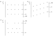
1つの実施形態においては、カメラを用いて、上記被検出部の位置を検出する。
1つの実施形態においては、幅方向において上記帯状フィルムを切り抜く前に、該帯状フィルムの幅方向の片側端辺を検出することと、該帯状フィルムを切り抜く際、切り抜き手段を、該帯状フィルムの幅方向の一方から他方へ向けて、移動させることとを含み、検出された該片側端辺を基準に、該切り抜き手段の移動方向を決定する。
本発明の別の局面によれば、光学フィルムの製造装置が提供される。この光学フィルムの製造装置は、帯状フィルムを所定の長さ方向送りピッチで搬送する搬送手段と、該帯状フィルムが有する被検出部を検出する検出手段と、該帯状フィルムの幅方向の一方から他方へ向けて移動し、かつ、検出された該被検出部の位置を基準として切り抜き線の位置決めを行う切り抜き手段とを含む。
1つの実施形態においては、上記検出手段が、上記帯状フィルムの幅方向の片側端辺をさらに検出し、検出された該片側端辺を基準に、上記切り抜き手段の移動方向が決定される。
11 被検出部(機能部)
12 切り抜き線
20 切り抜き手段(トムソン刃)
30 検出手段
100 帯状フィルム
Claims (5)
- 幅方向に2個以上および長さ方向に2個以上の被検出部を有する帯状フィルムを、所定の長さ方向送りピッチごとに、該帯状フィルムの幅方向の一方から他方へ向けて、順次切り抜くことを含み、
該帯状フィルムを切り抜く際、該被検出部の位置を検出し、検出された該被検出部の位置を基準として切り抜き線の位置決めを行い、検出された該被検出部を有するフィルム片を1枚ずつ得ることを含み、
該帯状フィルムが、長尺状偏光子であり、
該被検出部が、非偏光部である、
光学フィルムの製造方法。 - カメラを用いて、前記被検出部の位置を検出する、請求項1に記載の光学フィルムの製造方法。
- 幅方向において前記帯状フィルムを切り抜く前に、該帯状フィルムの幅方向の片側端辺を検出することと、
該帯状フィルムを切り抜く際、切り抜き手段を、該帯状フィルムの幅方向の一方から他方へ向けて、移動させることとを含み、
検出された該片側端辺を基準に、該切り抜き手段の移動方向を決定する、
請求項1または2に記載の光学フィルムの製造方法。 - 帯状フィルムを所定の長さ方向送りピッチで搬送する搬送手段と、
該帯状フィルムが有する被検出部を検出する検出手段と、
該帯状フィルムの幅方向の一方から他方へ向けて移動し、かつ、検出された該被検出部の位置を基準として切り抜き線の位置決めを行う切り抜き手段とを含み、
該帯状フィルムが、長尺状偏光子であり、
該被検出部が、非偏光部である、
光学フィルムの製造装置。 - 前記検出手段が、前記帯状フィルムの幅方向の片側端辺をさらに検出し、
検出された該片側端辺を基準に、前記切り抜き手段の移動方向が決定される、
請求項4に記載の製造装置。
Priority Applications (7)
| Application Number | Priority Date | Filing Date | Title |
|---|---|---|---|
| JP2014243855A JP6146921B2 (ja) | 2014-12-02 | 2014-12-02 | 光学フィルムの製造方法および製造装置 |
| PCT/JP2015/083040 WO2016088619A1 (ja) | 2014-12-02 | 2015-11-25 | 光学フィルムの製造方法および製造装置 |
| CN201580002766.6A CN107041131A (zh) | 2014-12-02 | 2015-11-25 | 光学薄膜的制造方法及制造装置 |
| CN202010293483.4A CN111483004A (zh) | 2014-12-02 | 2015-11-25 | 光学薄膜的制造方法及制造装置 |
| KR1020167012936A KR101757604B1 (ko) | 2014-12-02 | 2015-11-25 | 광학 필름의 제조 방법 및 제조 장치 |
| CN202210117239.1A CN114236665A (zh) | 2014-12-02 | 2015-11-25 | 光学薄膜的制造方法及制造装置 |
| TW104140113A TWI667111B (zh) | 2014-12-02 | 2015-12-01 | Optical film manufacturing method and manufacturing device |
Applications Claiming Priority (1)
| Application Number | Priority Date | Filing Date | Title |
|---|---|---|---|
| JP2014243855A JP6146921B2 (ja) | 2014-12-02 | 2014-12-02 | 光学フィルムの製造方法および製造装置 |
Publications (3)
| Publication Number | Publication Date |
|---|---|
| JP2016109722A JP2016109722A (ja) | 2016-06-20 |
| JP2016109722A5 JP2016109722A5 (ja) | 2017-03-09 |
| JP6146921B2 true JP6146921B2 (ja) | 2017-06-14 |
Family
ID=56091567
Family Applications (1)
| Application Number | Title | Priority Date | Filing Date |
|---|---|---|---|
| JP2014243855A Active JP6146921B2 (ja) | 2014-12-02 | 2014-12-02 | 光学フィルムの製造方法および製造装置 |
Country Status (5)
| Country | Link |
|---|---|
| JP (1) | JP6146921B2 (ja) |
| KR (1) | KR101757604B1 (ja) |
| CN (3) | CN111483004A (ja) |
| TW (1) | TWI667111B (ja) |
| WO (1) | WO2016088619A1 (ja) |
Cited By (1)
| Publication number | Priority date | Publication date | Assignee | Title |
|---|---|---|---|---|
| JP2017068062A (ja) * | 2015-09-30 | 2017-04-06 | 日東電工株式会社 | 偏光板の製造方法 |
Families Citing this family (1)
| Publication number | Priority date | Publication date | Assignee | Title |
|---|---|---|---|---|
| KR20220169754A (ko) | 2021-06-21 | 2022-12-28 | 최은지 | 입체퍼즐을 이용한 혼합현실 체감형 학습 교구 |
Family Cites Families (20)
| Publication number | Priority date | Publication date | Assignee | Title |
|---|---|---|---|---|
| US3200373A (en) * | 1960-11-22 | 1965-08-10 | Control Data Corp | Handwritten character reader |
| FR2570315B1 (fr) * | 1984-09-18 | 1988-06-10 | Loriot Jean Marc | Procede de reperage de la position et de la forme de gabarits disposes sur un materiau en plaque ou en feuille |
| DE4100534C1 (ja) * | 1991-01-10 | 1992-01-23 | Duerkopp Systemtechnik Gmbh, 4800 Bielefeld, De | |
| TW473619B (en) * | 1997-04-16 | 2002-01-21 | Sumitomo Chemical Co | Method for producing an optical film chip and optical film chip intermediate |
| JPH11231129A (ja) | 1997-11-17 | 1999-08-27 | Sumitomo Chem Co Ltd | 光学フィルム積層中間体およびその製造方法ならびに光学フィルム積層チップの製造方法 |
| JP3713183B2 (ja) * | 2000-04-26 | 2005-11-02 | リンテック株式会社 | 偏光板付剥離シート、その製造方法、偏光板の剥離方法及びその剥離装置 |
| EP1157793A1 (de) * | 2000-05-26 | 2001-11-28 | Thea Felber | Vorrichtung und Verfahren zum Ausrichten eines Zuschnittmusters auf der Oberfläche eines Materials |
| DE20009427U1 (de) * | 2000-05-26 | 2000-09-28 | Felber Thea | Vorrichtung zur Bearbeitung eines Materials oder eines Gegenstandes |
| JP2001350130A (ja) * | 2000-06-07 | 2001-12-21 | Ricoh Co Ltd | 液晶表示素子用フィルム切断装置及びこれに用いるフィルム |
| US6672187B2 (en) * | 2001-04-05 | 2004-01-06 | Mikkelsen Graphic Engineering, Inc. | Method and apparatus for rapid precision cutting of graphics areas from sheets |
| JP2003015120A (ja) * | 2001-06-27 | 2003-01-15 | Mitsuboshi Diamond Industrial Co Ltd | 液晶表示パネル製造方法 |
| JP2003019697A (ja) * | 2001-07-06 | 2003-01-21 | Eastern Giken Kk | 枚葉シート打抜き製造機における送り制御装置 |
| JP4376558B2 (ja) * | 2002-07-04 | 2009-12-02 | 富士フイルム株式会社 | 偏光板貼合方法及び装置 |
| JP2006337630A (ja) * | 2005-06-01 | 2006-12-14 | Sumitomo Chemical Co Ltd | 積層光学フィルムの製造方法 |
| DE102006037432C5 (de) * | 2006-08-09 | 2014-08-14 | Leonhard Kurz Gmbh & Co. Kg | Verfahren zur Herstellung mindestens einer Fensteröffnung in einem langgestreckten Papiersubstrat, sowie Vorrichtung |
| JP5221164B2 (ja) * | 2008-02-15 | 2013-06-26 | 日東電工株式会社 | 光学フィルム積層体の製造方法 |
| US8924002B2 (en) * | 2011-04-22 | 2014-12-30 | I-Cut, Inc. | Adaptive registration during precision graphics cutting from multiple sheets |
| JP5945143B2 (ja) * | 2011-05-20 | 2016-07-05 | 日東電工株式会社 | 光学フィルムロールセットおよび光学フィルムロールセットの製造方法。 |
| CN104145211B (zh) * | 2012-02-29 | 2017-03-29 | 住友化学株式会社 | 光学显示设备的生产系统以及光学显示设备的生产方法 |
| TWI616293B (zh) * | 2012-04-04 | 2018-03-01 | 住友化學股份有限公司 | 薄膜切斷方法及薄膜切斷系統 |
-
2014
- 2014-12-02 JP JP2014243855A patent/JP6146921B2/ja active Active
-
2015
- 2015-11-25 CN CN202010293483.4A patent/CN111483004A/zh active Pending
- 2015-11-25 WO PCT/JP2015/083040 patent/WO2016088619A1/ja active Application Filing
- 2015-11-25 CN CN201580002766.6A patent/CN107041131A/zh active Pending
- 2015-11-25 CN CN202210117239.1A patent/CN114236665A/zh active Pending
- 2015-11-25 KR KR1020167012936A patent/KR101757604B1/ko active IP Right Grant
- 2015-12-01 TW TW104140113A patent/TWI667111B/zh active
Cited By (1)
| Publication number | Priority date | Publication date | Assignee | Title |
|---|---|---|---|---|
| JP2017068062A (ja) * | 2015-09-30 | 2017-04-06 | 日東電工株式会社 | 偏光板の製造方法 |
Also Published As
| Publication number | Publication date |
|---|---|
| TW201627119A (zh) | 2016-08-01 |
| JP2016109722A (ja) | 2016-06-20 |
| CN107041131A (zh) | 2017-08-11 |
| TWI667111B (zh) | 2019-08-01 |
| CN114236665A (zh) | 2022-03-25 |
| KR101757604B1 (ko) | 2017-07-12 |
| CN111483004A (zh) | 2020-08-04 |
| WO2016088619A1 (ja) | 2016-06-09 |
| KR20160087809A (ko) | 2016-07-22 |
Similar Documents
| Publication | Publication Date | Title |
|---|---|---|
| JP6146921B2 (ja) | 光学フィルムの製造方法および製造装置 | |
| JP6872312B2 (ja) | 偏光板の製造方法 | |
| JP5273354B2 (ja) | 帯状部材の幅方向端部位置測定方法及びその装置 | |
| CN109029309A (zh) | 一种对线宽量测机进行校准的方法 | |
| JP2016129212A5 (ja) | ||
| US10429751B2 (en) | Alignment mark searching method, display substrate and display apparatus | |
| KR20170038688A (ko) | 편광자의 검사 방법 및 편광판의 제조 방법 | |
| EP3316037A3 (en) | An overlay measurement method and apparatus | |
| MX2019000751A (es) | Dispositivo de deteccion de posicion de substrato. | |
| TWI541548B (zh) | A manufacturing system for an optical film roll, and a method for manufacturing an optical film roll | |
| WO2016088600A1 (ja) | 切込線形成方法及び切込線形成装置 | |
| JP2016109722A5 (ja) | ||
| JP2014130140A (ja) | 測定結果検証システム | |
| TW201443521A (zh) | 檢測裝置、雷射光照射裝置及光學組件貼合體之製造裝置 | |
| US9247635B2 (en) | Flexible substrate | |
| EP3315897B1 (en) | Web detection device and detection method | |
| JP6666101B2 (ja) | 長尺状偏光子の検査方法 | |
| KR102345439B1 (ko) | 롤투롤 노광 시스템 | |
| JP6556008B2 (ja) | 長尺状偏光子の検査方法 | |
| JP2017090603A (ja) | 金属配線付光学積層体の製造方法 | |
| JP6695670B2 (ja) | 偏光板の製造方法 | |
| KR20170082079A (ko) | 이동식 검사장비를 이용한 기재의 결함 유무 검출 시스템 및 그 시스템을 통한 기재의 결함 유무 검출 방법 | |
| JP2017090604A (ja) | 金属配線付光学積層体の製造方法 | |
| JP2017068123A (ja) | 長尺状偏光子の検査方法 |
Legal Events
| Date | Code | Title | Description |
|---|---|---|---|
| A521 | Request for written amendment filed |
Free format text: JAPANESE INTERMEDIATE CODE: A523 Effective date: 20170201 |
|
| A621 | Written request for application examination |
Free format text: JAPANESE INTERMEDIATE CODE: A621 Effective date: 20170201 |
|
| A131 | Notification of reasons for refusal |
Free format text: JAPANESE INTERMEDIATE CODE: A131 Effective date: 20170301 |
|
| A521 | Request for written amendment filed |
Free format text: JAPANESE INTERMEDIATE CODE: A523 Effective date: 20170421 |
|
| TRDD | Decision of grant or rejection written | ||
| A01 | Written decision to grant a patent or to grant a registration (utility model) |
Free format text: JAPANESE INTERMEDIATE CODE: A01 Effective date: 20170510 |
|
| A61 | First payment of annual fees (during grant procedure) |
Free format text: JAPANESE INTERMEDIATE CODE: A61 Effective date: 20170515 |
|
| R150 | Certificate of patent or registration of utility model |
Ref document number: 6146921 Country of ref document: JP Free format text: JAPANESE INTERMEDIATE CODE: R150 |
|
| R250 | Receipt of annual fees |
Free format text: JAPANESE INTERMEDIATE CODE: R250 |
|
| R250 | Receipt of annual fees |
Free format text: JAPANESE INTERMEDIATE CODE: R250 |
|
| R250 | Receipt of annual fees |
Free format text: JAPANESE INTERMEDIATE CODE: R250 |
|
| R250 | Receipt of annual fees |
Free format text: JAPANESE INTERMEDIATE CODE: R250 |