JP6057538B2 - Imaging device - Google Patents
Imaging device Download PDFInfo
- Publication number
- JP6057538B2 JP6057538B2 JP2012102873A JP2012102873A JP6057538B2 JP 6057538 B2 JP6057538 B2 JP 6057538B2 JP 2012102873 A JP2012102873 A JP 2012102873A JP 2012102873 A JP2012102873 A JP 2012102873A JP 6057538 B2 JP6057538 B2 JP 6057538B2
- Authority
- JP
- Japan
- Prior art keywords
- image sensor
- plate
- unit
- standing wall
- imaging
- Prior art date
- Legal status (The legal status is an assumption and is not a legal conclusion. Google has not performed a legal analysis and makes no representation as to the accuracy of the status listed.)
- Active
Links
Images


Classifications
-
- H—ELECTRICITY
- H04—ELECTRIC COMMUNICATION TECHNIQUE
- H04N—PICTORIAL COMMUNICATION, e.g. TELEVISION
- H04N23/00—Cameras or camera modules comprising electronic image sensors; Control thereof
- H04N23/50—Constructional details
- H04N23/54—Mounting of pick-up tubes, electronic image sensors, deviation or focusing coils
Description
本発明は、撮像素子を有する撮像装置に関する。 The present invention relates to an imaging apparatus having an imaging element.
デジタル一眼レフカメラでは、撮像素子のパッケージ部材の一部から平板状の取り付け部を延出し、撮像装置本体に配置される板金部材等にビスで締結する撮像素子保持方法が知られている。しかしながら、ビス締結による保持方法を用いた場合、ビスの取り付けに要するスペースが必要となるため、撮像装置が大型化してしまうという問題がある。 In a digital single-lens reflex camera, there is known an image sensor holding method in which a flat mounting portion is extended from a part of a package member of an image sensor and fastened with a screw to a sheet metal member or the like arranged in the image pickup apparatus main body. However, when the holding method by screw fastening is used, there is a problem that a space required for screw attachment is required, and the imaging apparatus is increased in size.
そこで、接着用の開口部を有する保持板金を撮像装置本体において撮像素子の裏面と対向する位置に配置し、撮像素子の裏面と保持板金とを密着させた状態で開口部に接着剤を塗布して撮像素子を保持板金に固定する方法が知られている(特許文献1参照)。この方法によれば、前述のビス締結を行う場合に必要なビスの取り付けスペースが不要になるため、撮像装置を小型化することが可能になる。 Therefore, a holding sheet metal having an opening for bonding is disposed at a position facing the back surface of the imaging element in the image pickup apparatus body, and an adhesive is applied to the opening in a state where the back surface of the imaging element and the holding sheet metal are in close contact with each other. A method of fixing the image sensor to a holding metal plate is known (see Patent Document 1). According to this method, the screw mounting space required when the above-described screw fastening is performed becomes unnecessary, and the imaging apparatus can be downsized.
ここで、近年では、撮像素子と撮像素子を実装する撮像素子基板の生産性を高めるために、撮像素子基板に対して撮像素子を自動機により自動実装する技術が進んでいる。この場合、撮像素子の背面は撮像素子基板に覆われた状態となるため、前述した特許文献1に記載されているような撮像素子の固定方法を用いることはできない。
Here, in recent years, in order to increase the productivity of an image pickup device and an image pickup device substrate on which the image pickup device is mounted, a technology for automatically mounting the image pickup device on the image pickup device substrate by an automatic machine has been advanced. In this case, since the back surface of the image sensor is covered with the image sensor substrate, the fixing method of the image sensor as described in
また、撮像装置では、品質面から、撮像装置が落下等によって衝撃を受けたときでも、破壊することなく、また、撮像機能に不具合が生じることのない、強固な構造が求められている。そのため、衝撃を受けた場合でも、撮像素子の位置が保持される強固な撮像素子の保持構造が必要となる。特に、デジタル一眼レフカメラでは、衝撃等に不利な大型で重量がある撮像素子が用いられるため、撮像素子の保持を強固に行う必要がある。 In addition, the imaging device is required to have a robust structure that does not break down and that does not cause a malfunction in the imaging function even when the imaging device is impacted by dropping or the like. For this reason, a robust image sensor holding structure that holds the position of the image sensor even when subjected to an impact is required. In particular, in a digital single-lens reflex camera, since a large-sized and heavy image sensor that is disadvantageous to impact or the like is used, it is necessary to firmly hold the image sensor.
本発明は、撮像素子をコンパクトに、且つ、高い強度で固定することを目的とする。 An object of this invention is to fix an image pick-up element compactly and with high intensity | strength.
本発明に係る撮像装置は、配線基板と、前記配線基板に実装された撮像素子と、前記撮像素子が位置決め固定される固定部材とを備える撮像装置であって、前記固定部材は、前記撮像素子の撮像面を露出させる開口部と、前記開口部の外周において前記撮像素子と当接する当接面と、前記撮像素子の側面と対向するように前記当接面から立設される立壁部と、を有し、前記配線基板において前記撮像素子が実装された面が所定の間隔を空けて前記当接面と対向する状態で、前記撮像素子は前記当接面と当接し、前記撮像素子の側面と、前記立壁部において前記撮像素子の側面と対向する側面と、前記当接面の3つの面によって形成される溝形状の空間において前記3つの面に接する接着剤により前記撮像素子が前記固定部材に固定され、前記配線基板は前記空間を覆わないことを特徴とする。 An imaging apparatus according to the present invention is an imaging apparatus including a wiring board, an imaging element mounted on the wiring board, and a fixing member on which the imaging element is positioned and fixed. The fixing member includes the imaging element. An opening that exposes the imaging surface, an abutting surface that abuts the imaging element on an outer periphery of the opening, and a standing wall that is erected from the abutting surface so as to face a side surface of the imaging element; And the image sensor is in contact with the contact surface at a predetermined interval with the surface on which the image sensor is mounted facing the contact surface, and the side surface of the image sensor The imaging element is fixed to the fixing member by an adhesive contacting the three surfaces in a groove-shaped space formed by the three surfaces of the standing wall portion and the side surface of the imaging device facing the side surface. is secured to, the Line substrate is characterized by not covering the space.
本発明によれば、撮像素子をコンパクトに、且つ、高い強度で固定部材に固定することができる。 According to the present invention, the imaging device can be fixed to the fixing member in a compact and high strength.
以下、本発明の実施形態について、添付図面を参照して詳細に説明する。ここでは、撮像素子が配線基板(以下「基板」と記す)に対して自動実装され、撮像素子と基板とが一体化された撮像素子ユニットが、固定部材に固定される構造を取り上げる。 Hereinafter, embodiments of the present invention will be described in detail with reference to the accompanying drawings. Here, a structure is described in which an imaging element is automatically mounted on a wiring board (hereinafter referred to as “substrate”), and an imaging element unit in which the imaging element and the board are integrated is fixed to a fixing member.
<撮像素子ユニットの概略構成>
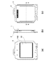
図1は、本実施形態に係る撮像装置が備える撮像素子ユニット1の概略構造を示す図であり、(a)は正面図を、(b)は右側面図(図1(a)を右側から見た図)を、(c)は背面図をそれぞれ示している。撮像素子ユニット1は、撮像素子10が自動実装により配線基板11(以下「基板11」と記する)に実装され、一体化されたものである。
<Schematic configuration of image sensor unit>
1A and 1B are diagrams illustrating a schematic structure of an
撮像素子10は、その内部に光電変換部(不図示)を有しており、撮像装置が備える光学系部材(不図示)を通して得た光学像を電気信号へ変換する。撮像素子10の外観を成す筺体であるパッケージ101は、撮像素子10の内部の光電変換部等の構成要素を保持しており、パッケージ101の正面側の表面はカバーガラス102によって覆われている。
The
パッケージ101において対向する一対の辺(本実施形態では長辺)にはリード103a,103bが設けられており、リード103a,103bは撮像素子10の内部の光電変換部と電気的に接続されている。パッケージ101において対向する別の一対の辺の側面であるパッケージ側面105a,105bは、露出した状態となっている。パッケージ101の表面において、パッケージ側面105a,105bと略平行なカバーガラス102の側面とパッケージ側面105a,105bとの間の領域は、プレート2(図2を参照して後述する)と当接するパッケージ側当接面104a,104bとなっている。
基板11は、リード103a,103bを介して撮像素子10の光電変換部と電気的に接続され、撮像素子10から電気信号を受け取る。基板11の背面側には、不図示の撮像装置本体と電気的に接続される基板コネクタ112が配設されている。また、撮像素子10の背面と基板11の表面との間には、空隙部(スタンドオフ)12が設けられている。
The
撮像装置の全体構成についての図示は省略するが、撮像装置において、撮像素子ユニット1の正面側前方には光学レンズ等で構成された光学系部材が配置される。光学系部材を通して撮像素子ユニット1に入力される光学像は、透明なカバーガラス102を通過して、撮像素子10の内部の光電変換部において結像する。
Although illustration of the entire configuration of the imaging apparatus is omitted, in the imaging apparatus, an optical system member constituted by an optical lens or the like is disposed in front of the
撮像素子10の光電変換部は、光を検出して電荷を発生させるフォトダイオード等で構成されている。撮像素子10は、具体的には、CCDセンサやCMOSセンサ等である。また、撮像素子10は、例えば、リード103a,103bをセラミック板で挟んでパッケージ101を構成し、パッケージ101の外側でリード103a,103bが基板11に半田付けされ、パッケージ101の裏面と基板11の表面との間に空隙部12が形成されたサーディップタイプの構造を有する。但し、撮像素子10は、このような構成に限定されるものではない。例えば、パッケージの裏面に電極パッドを設け、リードをパッケージ外側に出さないLLCC(Lead Less Chip Carrier)タイプの撮像素子を用いることも可能である。
The photoelectric conversion unit of the
撮像素子10のリード103a,103bは、基板11のランド部(不図示)に対して自動実装により半田付けされることで電気的に接続され、これにより、撮像素子10は基板11と機械的に一体化される。なお、基板11は、フレキシブルケーブル(FPC)等の可撓性を持った基板であってもよい。
The
カバーガラス102はパッケージ101の表面に重ねた状態でパッケージ101に対して接着固定され、図1(b)に示すように、カバーガラス102は、パッケージ101の表面から正面側に突出している。図1(c)に示すように、基板11においてパッケージ101が取り付けられる部分では、パッケージ側面105a,105bと略平行な基板端111a,111b間の幅寸法は、パッケージ側面105a,105b間の幅寸法以下となっている。そのため、撮像素子ユニット1を背面側からみると、パッケージ側面105a,105bが露出した状態となる。
なお、本実施形態では、上述の通り、パッケージ側面105a,105bの全体が基板端111a,111bから外側に突出して露出する構造とした。しかし、これに限られず、パッケージ側面105a,105bの一部が基板11の基板端111a,111bから突出して露出するように、基板11の形状を設計してもよい。
In the present embodiment, as described above, the entire
撮像素子10の内部の光電変換部から出力されたアナログ電気信号は、リード103a,103bを介して基板11へ伝達される。アナログ電気信号は、基板11の基板コネクタ112を介して、不図示の撮像装置本体に配置されるメイン基板へと伝達される。メイン基板に設けられた制御回路は、アナログ電気信号をデジタル信号に変換した後、圧縮や記録等の所定の処理を行う。
An analog electrical signal output from the photoelectric conversion unit inside the
<撮像素子ユニット1が位置決め固定されるプレート2の構造>
図2は、撮像素子ユニット1が位置決め固定される固定部材の一例であるプレート2の構造を示す図であり、(a)は背面図、(b)は底面図、(c)は背面斜視図である。なお、本実施形態では、プレート2について、図2(a)の左右方向を「幅方向」と定義する。
<Structure of
2A and 2B are diagrams showing the structure of the
プレート2は、例えば、ステンレス等の金属プレス加工により作製された板金部材である。プレート2の平面部21には、その正面側と背面側とを貫通する開口部22と、プレート2を不図示の撮像装置本体に対して位置決めするための一対の位置決め穴26が形成されている。開口部22は、後述するように、撮像素子ユニット1がプレート2に配置された状態で撮像素子10の撮像面を露出させるために設けられている。本実施形態では、一対の位置決め穴26を丸穴と長穴で構成しているが、このような形状に限定されるものではない。一対の位置決め穴26と撮像装置本体の位置決めボス(不図示)とを嵌合させることにより、プレート2は撮像装置本体に対して位置決めされ、固定される。
The
プレート2において開口部22を挟んで幅方向で対向する一対の辺には、プレート2の背面側に立設された一対の立壁部23a,23bが形成されている。平面部21における開口部22と立壁部23aとの間の領域は、撮像素子ユニット1をプレート2に位置決め固定する際にパッケージ側当接面104aと当接するプレート側当接面24aとなっている。同様に、平面部21における開口部22と立壁部23bとの間の領域は、撮像素子ユニット1をプレート2に固定する際にパッケージ側当接面104bと当接するプレート側当接面24bとなっている。
In the
撮像素子ユニット1をプレート2に固定して構成される撮像素子プレートユニットに熱伝導シートユニット4(図9参照)を組み込むために、立壁部23aの端部には凸部が形成され、立壁部23bの端部には凹部が形成される。凸部25a及び凹部25bの機能の詳細については後述する。
In order to incorporate the heat conductive sheet unit 4 (see FIG. 9) into the imaging element plate unit configured by fixing the
<プレート2に対する撮像素子ユニット1の位置決め固定>
図3は、プレート2に対する撮像素子ユニット1の位置決め固定方法を示す側面図であり、図1(b)と同様に撮像素子ユニット1の右側面図として示している。図3に示すように、撮像素子ユニット1は、プレート2の背面側からプレート2に対して矢印A方向、立壁部23a,23bによって挟まれた領域に撮像素子10が収容されるように、配置される。そのため、撮像素子10において立壁部23a,23bと対向する二辺であるパッケージ側面105a,105b間の幅寸法は、立壁部23a,23bの間の幅寸法より狭くなっている。
<Positioning and Fixing of
FIG. 3 is a side view showing a method for positioning and fixing the
図4は、図3の位置決め固定方法に従って撮像素子ユニット1をプレート2に対して配置した後の状態を示す図であり、(a)は正面図、(b)は右側面図(図4(a)を右側から見た図)、(c)は背面図である。
4A and 4B are diagrams showing a state after the
図4(a)に示すように、撮像素子10は、パッケージ101の表面側に突出しているカバーガラス102が、プレート2の開口部22に入り込むようにプレート2に対して組み込まれる。このとき、撮像素子ユニット1は、撮像素子10の内部の光電変換部の中心がプレート2に対して設計上の理想的な位置に収まるように位置調整されるが、その詳細については後述する。そして、前述の通り、プレート2は撮像装置本体に対して一定の位置に組み込まれるため、撮像素子ユニット1も撮像装置本体に対して理想的な位置に位置決めすることができる。
As shown in FIG. 4A, the
図5は、図4(c)に示す矢視S−S断面図であり、撮像素子ユニット1をプレート2に組み込んだ後、接着剤による接着固定を行う前の状態を示している。撮像素子ユニット1をプレート2に接着するための接着剤は、ディスペンサ30の内部に充填されており、ディスペンサ30の先端の射出部31(図6参照)から射出される。本実施形態では、接着剤として、紫外線硬化樹脂等の光硬化性樹脂を用いる。これは、光硬化性樹脂を用いることにより、接着剤を短時間で硬化させることができるため、接着固定に要する時間を短縮して、生産効率の向上を図ることができるからである。
FIG. 5 is a cross-sectional view taken along the line SS shown in FIG. 4C, and shows a state before the
ディスペンサ30は、撮像素子ユニット1のパッケージ側面105a,105bとプレート2の立壁部23a,23bとの間の空間へ、撮像素子ユニット1の背面側から挿入される。このとき、基板11の基板端111a,111b間の距離がパッケージ101のパッケージ側面105a,105b間の距離よりも短い。すなわち、立壁部23aから基板11の立壁部23aに対向する基板端111aまでの距離が立壁部23aから撮像素子ユニット1のパッケージ側面105aまでの距離よりも長くなる。このため、基板11がディスペンサ30の挿入の妨げにならず、ディスペンサ30を容易に所定位置に挿入することができる。
The
このように本実施形態では、自動実装により撮像素子10が基板11に実装された撮像素子ユニット1であっても、省スペースで撮像素子ユニット1をプレート2に対して接着固定することができる。また、接着剤として光硬化性樹脂を使用する場合には、塗布後に接着剤に対して光照射が必要となるが、背面視においてパッケージ側面105a,105bが露出しているため、塗布された接着剤に対して背面側から容易に光照射を行うことができる。なお、本実施形態では、パッケージ側面105a,105bの全体が露出するように基板11の形状を設計しているが、パッケージ側面105a,105bの一部が露出する形状であってもよい。
As described above, in the present embodiment, even if the
図5に示す幅寸法Wは、プレート2の幅方向での最大幅を表している。この幅寸法Wについては、図6を参照した説明の際に、併せて説明する。
The width dimension W shown in FIG. 5 represents the maximum width of the
図6は、図5に示すT部の拡大図である。撮像素子ユニット1がプレート2に組み込まれた状態では、プレート側当接面24aにパッケージ側当接面104aが乗り、プレート側当接面24aとパッケージ側当接面104aとが密着する。図6に示す寸法βは、撮像素子ユニット1がプレート2に組み込まれた状態において、カバーガラス102の端面と開口部22の側面との間に形成されるクリアランスを示している。また、図6に示す寸法αは、プレート側当接面24aとパッケージ側当接面104aとのオーバーラップ量を示している。撮像素子ユニット1をプレート2に組み込む際に、寸法αの領域で撮像素子ユニット1がプレート2に突きあたることによって、撮像素子ユニット1とプレート2との組み込み方向(図3の矢印A方向)における相対的位置が定まる。
FIG. 6 is an enlarged view of a T portion shown in FIG. In a state where the image
ディスペンサ30の先端(針先)の射出部31は、パッケージ側面105aと立壁部23aとの間に入り込んで接着剤を射出する。図6に示す寸法γは、パッケージ側面105aと立壁部23aとの間の空隙の幅寸法を表している。
The
[寸法α,β,γの設定]
前述の通り、カバーガラス102の端面と開口部22の側面との間には、プレート2の幅方向において寸法βのクリアランスが形成される。
[Setting of dimensions α, β, γ]
As described above, between the end surface and the side surface of the
撮像素子10の内部の光電変換部の中心がプレート2に対して理想的な位置にくるように、撮像素子ユニット1をプレート2に対して位置決めする必要がある。そこで、プレート2の幅方向における撮像素子ユニット1のプレート2に対する調整範囲±X(ばらつき幅)について検討する。
The
寸法αは、プレート2に対する撮像素子ユニット1の位置調整が行われた際に常にパッケージ側当接面104aがプレート側当接面24aに乗っているように、寸法設定される必要がある。つまり、“α>X”の関係が満たされている必要がある。また、寸法βは、“α>X”の関係が成立していることを前提として、カバーガラス102の側面と開口部22の側面とが干渉(衝突)しない寸法に設定する必要がある。したがって、“β>X”の関係が満たされている必要がある。寸法γは、プレート2に対する撮像素子ユニット1の位置がバラついても、必ずディスペンサ30の射出部31の直径(幅)よりも長い寸法とする必要がある。
The dimension α needs to be set so that the package-
寸法α、β、γを、上記条件を満たしつつ小型に特化した数値に設定することにより、例えば、従来のようにパッケージの一部から平板状の取り付け部を延出して撮像素子をビス固定する場合よりも、撮像素子ユニット1を幅方向において小型化することができる。すなわち、調整寸法±Xに基づいて寸法α,β,γを最小限の寸法に設定することにより、プレート2の幅寸法Wを最小限に設定して撮像装置に適用することにより、撮像装置を小型化することができる。
By setting the dimensions α, β, γ to numerical values specialized for small size while satisfying the above conditions, for example, a flat mounting part is extended from a part of the package as in the past, and the image sensor is fixed with screws The image
[接着剤の充填]
図6に示すように、接着剤が充填される空間(射出部31の先端から先方の空間)は、パッケージ側面105aとプレート側当接面24aと立壁部23aとによって三方を囲まれた袋形状(溝形状)の空間になっていることがわかる。このように、接着剤が充填される空間を袋形状の空間に構成することにより、接着剤がプレート2の幅方向に流れ出るのを防止する。この効果は、撮像素子ユニット1をプレート2に対して所定の力で押圧しながら接着剤を充填する場合に、より顕著に得ることができる。
[Adhesive filling]
As shown in FIG. 6, the space filled with the adhesive (the space ahead from the tip of the injection portion 31) is a bag shape surrounded on three sides by the
なお、撮像素子ユニット1とプレート2との接着方法としては、プレート2を固定し、位置調整治具を用いて撮像素子ユニット1をプレート2に対して組み込み方向に位置合わせした状態で保持して接着を行う接着方法(空中接着)も考えられる。しかし、この方法では、位置合わせの作業性がよいとはいえない。これに対して、本実施形態のように、プレート側当接面24aとパッケージ側当接面104aとを密着させた状態で接着を行う方法は、極めて作業性に優れており、よって、接着工程での作業ミスの発生を極めて少なくすることができる。
The
図7は、撮像素子ユニット1とプレート2とが接着剤により接着固定された状態を示す底面図(図2(c)と同様)である。なお、以下の説明では、撮像素子ユニット1とプレート2とが接着固定されて一体化されたものを「撮像素子プレートユニット」と称することとする。
FIG. 7 is a bottom view (similar to FIG. 2C) showing a state in which the
本実施形態では、ディスペンサ30の射出部31が挿入されるプレート2の幅方向の2つの面(図5参照)において、接着剤32による撮像素子ユニット1とプレート2との接着が行われる。具体的には、図5に示す状態で、接着剤32を射出させながらディスペンサ30をパッケージ側面105aに沿って移動させた後、射出した接着剤32を硬化させる。このとき、ディスペンサ30の位置と移動範囲を変えることによって、接着剤の射出位置及び射出範囲を変えることができる。つまり、接着剤の射出位置及び射出範囲は、適宜、設定可能である。そのため、例えば、パッケージ側面105aの一部が基板11の基板端111aから突出して露出した構成では、パッケージ側面105aの露出した部分のみに接着剤を充填して硬化させることができる。
In this embodiment, the
図8は、図7に示すU部の拡大図である。撮像素子ユニット1とプレート2とは、パッケージ側面105aとプレート側当接面24aと立壁部23aとによって三方を囲まれた袋形状の空間に接着剤32が充填されて固化されることにより、接着固定される。このようにプレート2に立壁部23aを設けることにより、パッケージ側面105aとプレート側当接面24aと立壁部23aの3つの面での接着が可能となる。
FIG. 8 is an enlarged view of the U portion shown in FIG. The
これにより、例えば、パッケージ側面105aとプレート側当接面24aの2つの面で接着する場合よりも、接着強度を向上させることができる。また、パッケージ側面105aと高強度なプレート2の立壁部23aとが接着剤32を介して一体化された状態となるため、撮像素子プレートユニットの全体的な機械的強度を高め、耐衝撃性を向上させることができる。なお、パッケージ側面105b側(立壁部23b側)についても、同様である。
Thereby, for example, the adhesive strength can be improved as compared with the case of bonding on the two surfaces of the
以上に説明してきたように、本実施形態によれば、撮像装置本体に対して、小型化された撮像素子プレートユニットを配設することができる。また、撮像素子ユニット1とプレート2との接着強度を高めることができると共に、撮像素子プレートユニットの全体的な強度、耐衝撃性を高めることができる。
As described above, according to the present embodiment, it is possible to dispose a miniaturized imaging element plate unit with respect to the imaging apparatus main body. In addition, the adhesive strength between the
<撮像素子10の発熱対策>
撮像素子10の発熱対策として、熱伝導シートを撮像素子プレートユニットに装着する方法について説明する。図9は、撮像素子プレートユニットに装着される熱伝導シートユニット4の斜視図であり、(a)は背面斜視図、(b)は正面斜視図である。
<Measures against Heat Generation of
As a countermeasure against heat generation of the
熱伝導シートユニット4は、撮像素子10の熱を外部に伝熱する熱伝導シート41と、熱伝導シート41を保持する薄板状ホルダ42と、薄板状ホルダ42に保持されるクッション43とを有する。熱伝導シート41は、撮像素子10側に配置される吸熱部411と、吸熱部411から伝導された熱を放熱する放熱部412とによって構成されている。熱伝導シート41としては、例えば、可撓性を有するグラファイトシートを用いることができるが、これに限定されるものではない。クッション43と熱伝導シート41の吸熱部411とは、薄板状ホルダ42の表裏にそれぞれ配置され、粘着剤により保持される。
The heat conductive sheet unit 4 includes a heat
図10は、撮像素子プレートユニットに対する熱伝導シートユニット4の組み付け方法を示す図である。撮像素子プレートユニットに対して、熱伝導シートユニット4は、図10の矢印B方向に挿入される。先ず、薄板状ホルダ42を、プレート2の立壁部23bに設けられた凹部25bに通すように挿入する。薄板状ホルダ42は、凹部25bを通過すると、図1(b)に示した空隙部12に進入する。このとき、薄板状ホルダ42の短辺に平行な方向での位置は、凹部25bの側壁面と薄板状ホルダ42の長辺側面とによって位置決めされる。ここで、プレート2の立壁部23bは第2の立壁部として機能する。
FIG. 10 is a diagram illustrating a method of assembling the heat conductive sheet unit 4 to the imaging element plate unit. The heat conductive sheet unit 4 is inserted in the direction of arrow B in FIG. 10 with respect to the imaging element plate unit. First, the
図11は、撮像素子プレートユニットに熱伝導シートユニット4が組み込まれた状態を示す背面図である。薄板状ホルダ42が空隙部12を通過していくと、立壁部23aに形成されている凸部25aに突きあたる。ここで、プレート2の立壁部23aは第1の立壁部として機能する。
FIG. 11 is a rear view showing a state in which the heat conductive sheet unit 4 is incorporated in the imaging element plate unit. When the thin plate-shaped
こうして、熱伝導シートユニット4の組み込み方向(図10の矢印B方向)での位置が決まるため、撮像素子プレートユニットに対して熱伝導シートユニット4を位置決めすることができ、吸熱部411を撮像素子10の裏面の略中心位置に収めることができる。これにより、撮像素子10の発熱範囲を確実に吸熱部411で覆って、撮像素子10からの放熱を確実に、且つ、均一に行うことができるようになる。
Thus, since the position of the heat conductive sheet unit 4 in the direction in which the heat conductive sheet unit 4 is assembled (the direction of arrow B in FIG. 10) is determined, the heat conductive sheet unit 4 can be positioned with respect to the image sensor plate unit. 10 can be accommodated at a substantially central position on the back surface. As a result, the heat generation range of the
図12は、図11に示す矢視V−V断面図である。凹部25bは、空隙部12を阻害しない範囲に設定され、凸部25aは空隙部12を覆う範囲に設定されている。クッション43は、空隙部12において基板11にチャージされ、薄板状ホルダ42を介して吸熱部411を撮像素子ユニット1(撮像素子10)に対して押し付ける。これにより、熱伝導シート41が安定して撮像素子ユニット1に接触し、撮像素子10の熱を吸熱することができる。吸熱部411によって撮像素子ユニット1から吸熱された熱は、放熱部412へと伝熱され、放熱部412によって不図示の放熱部品へと放熱されることで、撮像素子10の温度上昇が抑えられる。
FIG. 12 is a cross-sectional view taken along the line VV shown in FIG. The
以上の説明の通り、プレート2の立壁部23a,23bに凸部25a及び凹部25bを設けることで、撮像素子プレートユニットに対する熱伝導シートユニット4の位置決めを容易に行い、撮像素子ユニット1からの放熱を確実、且つ、均一に行うことができる。また、撮像素子ユニット1の空隙部12への熱伝導シートユニット4の進入が容易な構造となっているので、撮像素子プレートユニットに対する熱伝導シートユニットの組立性を向上させることができる。そして、これらの効果を、先に説明した通り、撮像素子プレートユニットを小型化し、高い強度と耐衝撃性とを得る効果と同時に得ることができる。
As described above, by providing the raised
<その他の実施形態>
以上、本発明をその好適な実施形態に基づいて詳述してきたが、本発明はこれら特定の実施形態に限られるものではなく、この発明の要旨を逸脱しない範囲の様々な形態も本発明に含まれる。例えば、上記実施形態では、撮像装置本体に対して固定されるプレート2に撮像素子ユニット1を接着固定するとしたが、撮像装置本体がプレート2と同等形状の部位を備え、この同等形状部位に撮像素子ユニット1を接着固定してもよい。
<Other embodiments>
Although the present invention has been described in detail based on preferred embodiments thereof, the present invention is not limited to these specific embodiments, and various forms within the scope of the present invention are also included in the present invention. included. For example, in the above-described embodiment, the
1 撮像素子ユニット
2 プレート
4 熱伝導シートユニット
10 撮像素子
11 基板(配線基板)
12 空隙部
21 平面部
23a,23b 立壁部
25a 凸部
25b 凹部
32 接着剤
DESCRIPTION OF
12
Claims (3)
前記固定部材は、
前記撮像素子の撮像面を露出させる開口部と、
前記開口部の外周において前記撮像素子と当接する当接面と、
前記撮像素子の側面と対向するように前記当接面から立設される立壁部と、を有し、
前記配線基板において前記撮像素子が実装された面が所定の間隔を空けて前記当接面と対向する状態で、前記撮像素子は前記当接面と当接し、
前記撮像素子の側面と、前記立壁部において前記撮像素子の側面と対向する側面と、前記当接面の3つの面によって形成される溝形状の空間において前記3つの面に接する接着剤により前記撮像素子が前記固定部材に固定され、
前記配線基板は前記空間を覆わないことを特徴とする撮像装置。 An imaging device comprising: a wiring board; an imaging device mounted on the wiring board; and a fixing member on which the imaging device is positioned and fixed.
The fixing member is
An opening that exposes the imaging surface of the imaging element;
A contact surface that comes into contact with the image sensor on the outer periphery of the opening;
A standing wall portion standing from the contact surface so as to face the side surface of the image sensor,
With the surface on which the image sensor is mounted on the wiring board facing the contact surface with a predetermined interval, the image sensor contacts the contact surface,
The imaging by the adhesive contacting the three surfaces in the groove-shaped space formed by the three surfaces of the side surface of the imaging device, the side surface of the standing wall portion facing the side surface of the imaging device, and the contact surface. An element is fixed to the fixing member ;
The imaging apparatus, wherein the wiring board does not cover the space .
前記立壁部は、前記開口部を挟んで対向する第1の立壁部及び第2の立壁部を有し、
前記第1の立壁部の端部は凸部を有し、
前記第2の立壁部の端部は凹部を有し、
前記撮像素子と前記配線基板との間には空隙部が形成され、前記熱伝導シートは、前記凹部に挿入され、且つ、前記凸部に当接した状態で前記空隙部に配置されていることを特徴とする請求項1又は2記載の撮像装置。 The imaging device includes a heat conductive sheet,
The standing wall has a first standing wall and a second standing wall facing each other across the opening,
The end of the first standing wall has a convex part,
The end of the second standing wall has a recess,
A gap is formed between the image sensor and the wiring board, and the thermal conductive sheet is inserted into the recess and disposed in the gap in a state of being in contact with the projection. imaging device according to claim 1 or 2 wherein.
Priority Applications (2)
| Application Number | Priority Date | Filing Date | Title |
|---|---|---|---|
| JP2012102873A JP6057538B2 (en) | 2012-04-27 | 2012-04-27 | Imaging device |
| US13/834,093 US9065989B2 (en) | 2012-04-27 | 2013-03-15 | Image pickup apparatus having image pickup device |
Applications Claiming Priority (1)
| Application Number | Priority Date | Filing Date | Title |
|---|---|---|---|
| JP2012102873A JP6057538B2 (en) | 2012-04-27 | 2012-04-27 | Imaging device |
Publications (3)
| Publication Number | Publication Date |
|---|---|
| JP2013232732A JP2013232732A (en) | 2013-11-14 |
| JP2013232732A5 JP2013232732A5 (en) | 2015-06-18 |
| JP6057538B2 true JP6057538B2 (en) | 2017-01-11 |
Family
ID=49476956
Family Applications (1)
| Application Number | Title | Priority Date | Filing Date |
|---|---|---|---|
| JP2012102873A Active JP6057538B2 (en) | 2012-04-27 | 2012-04-27 | Imaging device |
Country Status (2)
| Country | Link |
|---|---|
| US (1) | US9065989B2 (en) |
| JP (1) | JP6057538B2 (en) |
Families Citing this family (1)
| Publication number | Priority date | Publication date | Assignee | Title |
|---|---|---|---|---|
| JP6639290B2 (en) * | 2016-03-18 | 2020-02-05 | キヤノン株式会社 | Imaging device |
Family Cites Families (12)
| Publication number | Priority date | Publication date | Assignee | Title |
|---|---|---|---|---|
| US6147389A (en) * | 1999-06-04 | 2000-11-14 | Silicon Film Technologies, Inc. | Image sensor package with image plane reference |
| US6734419B1 (en) * | 2001-06-28 | 2004-05-11 | Amkor Technology, Inc. | Method for forming an image sensor package with vision die in lens housing |
| US7274094B2 (en) * | 2002-08-28 | 2007-09-25 | Micron Technology, Inc. | Leadless packaging for image sensor devices |
| JP4225860B2 (en) | 2003-07-29 | 2009-02-18 | Hoya株式会社 | Digital camera |
| JP2005121912A (en) * | 2003-10-16 | 2005-05-12 | Sony Corp | Lens barrel and photographing device |
| JP3827089B2 (en) * | 2003-10-20 | 2006-09-27 | ソニー株式会社 | Lens barrel and imaging device |
| KR100873248B1 (en) * | 2004-12-14 | 2008-12-11 | 세이코 프레시죤 가부시키가이샤 | Solid-state image pickup device and electronic device |
| US7750279B2 (en) * | 2006-02-23 | 2010-07-06 | Olympus Imaging Corp. | Image pickup apparatus and image pickup unit |
| JP2008312040A (en) * | 2007-06-15 | 2008-12-25 | Fujinon Corp | Photographing unit, photographing device, portable equipment, and method for assembling photographing unit |
| JP5376865B2 (en) * | 2008-08-19 | 2013-12-25 | キヤノン株式会社 | Solid-state imaging device and electronic imaging device |
| JP5064585B2 (en) * | 2010-06-14 | 2012-10-31 | パナソニック株式会社 | Shielding structure and imaging element support structure |
| KR101720772B1 (en) * | 2010-08-27 | 2017-04-03 | 삼성전자주식회사 | Imaging sensor assembly |
-
2012
- 2012-04-27 JP JP2012102873A patent/JP6057538B2/en active Active
-
2013
- 2013-03-15 US US13/834,093 patent/US9065989B2/en active Active
Also Published As
| Publication number | Publication date |
|---|---|
| JP2013232732A (en) | 2013-11-14 |
| US20130286281A1 (en) | 2013-10-31 |
| US9065989B2 (en) | 2015-06-23 |
Similar Documents
| Publication | Publication Date | Title |
|---|---|---|
| JP4405062B2 (en) | Solid-state imaging device | |
| US7733408B2 (en) | Optical device module, optical path fixing device, and method for manufacturing optical device module | |
| KR101455124B1 (en) | Image pickup apparatus having imaging sensor package | |
| CN101848326B (en) | Imaging apparatus | |
| JP6639290B2 (en) | Imaging device | |
| JP6057538B2 (en) | Imaging device | |
| JP2015015662A (en) | Imaging unit and imaging apparatus | |
| JP2018038054A (en) | Imaging unit and imaging apparatus | |
| JP4943413B2 (en) | Camera assembly structure | |
| JP2012083556A (en) | Camera module | |
| JP6149442B2 (en) | Imaging unit and imaging apparatus | |
| JP6191254B2 (en) | Imaging unit and imaging apparatus | |
| JP2015015529A (en) | Imaging unit and imaging apparatus | |
| JP6443494B2 (en) | Imaging unit and imaging apparatus | |
| JP6756357B2 (en) | Imaging device | |
| JP2013222772A (en) | Image pickup element package and image pickup device | |
| KR20020084541A (en) | Implementation of very thin imaging module for mobile equipments. | |
| JP6675241B2 (en) | Imaging device | |
| JP7078151B2 (en) | Imaging unit and imaging device | |
| JP6849016B2 (en) | Imaging unit and imaging device | |
| JP6145988B2 (en) | The camera module | |
| JP5601081B2 (en) | Imaging element unit and imaging apparatus | |
| KR100483721B1 (en) | Solid image taking apparatus | |
| JP6547799B2 (en) | Imaging unit and imaging apparatus | |
| JP2011211379A (en) | Imaging apparatus |
Legal Events
| Date | Code | Title | Description |
|---|---|---|---|
| A521 | Request for written amendment filed |
Free format text: JAPANESE INTERMEDIATE CODE: A523 Effective date: 20150424 |
|
| A621 | Written request for application examination |
Free format text: JAPANESE INTERMEDIATE CODE: A621 Effective date: 20150424 |
|
| A977 | Report on retrieval |
Free format text: JAPANESE INTERMEDIATE CODE: A971007 Effective date: 20160210 |
|
| A131 | Notification of reasons for refusal |
Free format text: JAPANESE INTERMEDIATE CODE: A131 Effective date: 20160301 |
|
| A521 | Request for written amendment filed |
Free format text: JAPANESE INTERMEDIATE CODE: A523 Effective date: 20160427 |
|
| A131 | Notification of reasons for refusal |
Free format text: JAPANESE INTERMEDIATE CODE: A131 Effective date: 20160531 |
|
| A521 | Request for written amendment filed |
Free format text: JAPANESE INTERMEDIATE CODE: A523 Effective date: 20160720 |
|
| TRDD | Decision of grant or rejection written | ||
| A01 | Written decision to grant a patent or to grant a registration (utility model) |
Free format text: JAPANESE INTERMEDIATE CODE: A01 Effective date: 20161108 |
|
| A61 | First payment of annual fees (during grant procedure) |
Free format text: JAPANESE INTERMEDIATE CODE: A61 Effective date: 20161206 |
|
| R151 | Written notification of patent or utility model registration |
Ref document number: 6057538 Country of ref document: JP Free format text: JAPANESE INTERMEDIATE CODE: R151 |