CN101848326B - Imaging apparatus - Google Patents
Imaging apparatus Download PDFInfo
- Publication number
- CN101848326B CN101848326B CN201010141137.0A CN201010141137A CN101848326B CN 101848326 B CN101848326 B CN 101848326B CN 201010141137 A CN201010141137 A CN 201010141137A CN 101848326 B CN101848326 B CN 101848326B
- Authority
- CN
- China
- Prior art keywords
- conversion element
- photoelectric conversion
- element package
- back side
- fixed component
- Prior art date
- Legal status (The legal status is an assumption and is not a legal conclusion. Google has not performed a legal analysis and makes no representation as to the accuracy of the status listed.)
- Expired - Fee Related
Links
- 238000003384 imaging method Methods 0.000 title abstract description 8
- 238000006243 chemical reaction Methods 0.000 claims abstract description 204
- 238000001816 cooling Methods 0.000 claims description 10
- 239000000463 material Substances 0.000 claims description 4
- 230000003287 optical effect Effects 0.000 description 22
- 230000007246 mechanism Effects 0.000 description 16
- RYGMFSIKBFXOCR-UHFFFAOYSA-N Copper Chemical compound [Cu] RYGMFSIKBFXOCR-UHFFFAOYSA-N 0.000 description 10
- 239000011889 copper foil Substances 0.000 description 10
- 238000005538 encapsulation Methods 0.000 description 10
- 238000009434 installation Methods 0.000 description 8
- 230000005540 biological transmission Effects 0.000 description 6
- 230000000694 effects Effects 0.000 description 6
- 230000002093 peripheral effect Effects 0.000 description 6
- 230000036544 posture Effects 0.000 description 4
- 239000000853 adhesive Substances 0.000 description 3
- 230000001070 adhesive effect Effects 0.000 description 3
- 230000017525 heat dissipation Effects 0.000 description 3
- 239000002184 metal Substances 0.000 description 3
- 229910052751 metal Inorganic materials 0.000 description 3
- 238000000034 method Methods 0.000 description 3
- 230000008569 process Effects 0.000 description 3
- 230000000630 rising effect Effects 0.000 description 3
- 230000005855 radiation Effects 0.000 description 2
- 229920003002 synthetic resin Polymers 0.000 description 2
- 239000000057 synthetic resin Substances 0.000 description 2
- 230000015572 biosynthetic process Effects 0.000 description 1
- 230000008859 change Effects 0.000 description 1
- 238000010276 construction Methods 0.000 description 1
- 238000006073 displacement reaction Methods 0.000 description 1
- 238000005516 engineering process Methods 0.000 description 1
- 230000004048 modification Effects 0.000 description 1
- 238000012986 modification Methods 0.000 description 1
- 238000000465 moulding Methods 0.000 description 1
- 230000037361 pathway Effects 0.000 description 1
- 229910000679 solder Inorganic materials 0.000 description 1
- 238000005476 soldering Methods 0.000 description 1
- 230000007704 transition Effects 0.000 description 1
Images


Classifications
-
- H—ELECTRICITY
- H01—ELECTRIC ELEMENTS
- H01L—SEMICONDUCTOR DEVICES NOT COVERED BY CLASS H10
- H01L27/00—Devices consisting of a plurality of semiconductor or other solid-state components formed in or on a common substrate
- H01L27/14—Devices consisting of a plurality of semiconductor or other solid-state components formed in or on a common substrate including semiconductor components sensitive to infrared radiation, light, electromagnetic radiation of shorter wavelength or corpuscular radiation and specially adapted either for the conversion of the energy of such radiation into electrical energy or for the control of electrical energy by such radiation
- H01L27/144—Devices controlled by radiation
- H01L27/146—Imager structures
- H01L27/14601—Structural or functional details thereof
- H01L27/14618—Containers
-
- H—ELECTRICITY
- H04—ELECTRIC COMMUNICATION TECHNIQUE
- H04N—PICTORIAL COMMUNICATION, e.g. TELEVISION
- H04N23/00—Cameras or camera modules comprising electronic image sensors; Control thereof
- H04N23/50—Constructional details
- H04N23/54—Mounting of pick-up tubes, electronic image sensors, deviation or focusing coils
-
- H—ELECTRICITY
- H01—ELECTRIC ELEMENTS
- H01L—SEMICONDUCTOR DEVICES NOT COVERED BY CLASS H10
- H01L2924/00—Indexing scheme for arrangements or methods for connecting or disconnecting semiconductor or solid-state bodies as covered by H01L24/00
- H01L2924/0001—Technical content checked by a classifier
- H01L2924/0002—Not covered by any one of groups H01L24/00, H01L24/00 and H01L2224/00
Abstract
An imaging apparatus includes a photoelectric conversion element package, a chassis member arranged at a position opposite a rear surface of the photoelectric conversion element package, a wiring member electrically connected to the photoelectric conversion element package. The wiring member has an opening that exposes the rear surface of the photoelectric conversion element package. The wiring member is arranged between the rear surface of the photoelectric conversion element package and the chassis member. The imaging apparatus further includes a heat conduction member configured to contact the rear surface of the photoelectric conversion element package, exposed by the opening, and the chassis member.
Description
Technical field
The present invention relates to a kind of picture pick-up device, this picture pick-up device has photoelectric conversion element package and adjusts photoelectric conversion element package (package) with respect to the mechanism of the inclination of optical axis orthogonal plane (with the plane of light shaft positive cross), especially, the picture pick-up device that relates to a kind of heat of the photoelectric conversion element package that is configured to leave.
Background technology
In such as picture pick-up devices such as digital cameras, along with the increase of the pixel count that is installed in the photo-electric conversion element in the equipment body, with higher precision that light receiving surface and the photographic lens imaging of optical systems of photo-electric conversion element is usually more and more higher in the face of the requirement of position (align).
Thereby, require picture pick-up device to comprise and can adjust photo-electric conversion element with respect to the mechanism of the position of lens barrel (lens barrel).
Therefore, traditional picture pick-up device is provided with the fixed component for the position of restriction (regulate) photoelectric conversion element package on the optical axis direction of lens barrel.So, after photoelectric conversion element package is fixed to fixed component, the relative position on optical axis direction between fine setting lens barrel and the fixed component.This so that the light receiving surface of photo-electric conversion element and photographic lens imaging of optical systems face with higher precision contraposition.
In addition, expectation photoelectric conversion element package, fixed component and the gross thickness that the printed circuit board (PCB) of photoelectric conversion element package is installed reduce, so that picture pick-up device miniaturization and slimming.
Thereby traditional picture pick-up device uses non-terminal type (leadless-type) photoelectric conversion element package.In addition, such as Fig. 1 in the Japanese kokai publication hei 11-261904 communique and shown in Figure 7, proposed by printed circuit board (PCB) being configured in the proposal that limits the position of photoelectric conversion element package and fixed component between photoelectric conversion element package and the fixed component.
In picture pick-up device in recent years, the heat that is produced by photo-electric conversion element increases along with the increase of the processing speed of photo-electric conversion element, thereby the temperature that causes photo-electric conversion element raises.The noise that is caused by the dark current of photo-electric conversion element increases along with the rising of temperature usually, thereby requires to reduce or the temperature that suppresses photo-electric conversion element raises to realize high-quality photographs.
In order to process this problem, TOHKEMY 2003-204457 communique has been discussed a kind of picture pick-up device that the heat that is produced by photo-electric conversion element is left and suppress the mechanism that the temperature of photo-electric conversion element raises that is provided with.
Yet traditional picture pick-up device comprises tilt adjusting mechanism, and this tilt adjusting mechanism can carry out photo-electric conversion element with respect to the tilt adjustments of the optical axis orthogonal plane of lens barrel.Tilt adjusting mechanism has fixed component, and this fixed component is configured in the back side of photoelectric conversion element package, is used for the position of restriction photoelectric conversion element package on optical axis direction.
The picture pick-up device that comprises this tilt adjusting mechanism places heat dissipation path with fixed component, to leave from the heat of photo-electric conversion element.
Fixed component is configured to contact with photoelectric conversion element package point via jut, with the position of restriction photoelectric conversion element package.Thereby, in this structure, be used for leaving and only conduct heat via the jut that contacts with photoelectric conversion element package point from the part of the heat dissipation path of the heat of photo-electric conversion element, therefore, the radiating efficiency of photo-electric conversion element may reduce.
In addition, when leaving from photo-electric conversion element hot via fixed component, require fixed component is configured so that can not damage photo-electric conversion element with respect to the function of the tilt adjustments of the optical axis orthogonal plane of lens barrel.Thereby, when leaving from photo-electric conversion element hot via fixed component, be difficult to make up strong heat dissipation path.
Summary of the invention
According to an aspect of the present invention, proposed a kind of camera head, this camera head comprises: photoelectric conversion element package; Rack component, it is configured in the position relative with the back side of photoelectric conversion element package; Wiring member, it is electrically connected to photoelectric conversion element package, and wherein, Wiring member has the opening of the back exposure of the photoelectric conversion element package of making, and Wiring member is configured between the back side and rack component of photoelectric conversion element package; And heat conduction member, it is configured to contact with the back side of rack component with the photoelectric conversion element package that exposes via opening.
According to a further aspect in the invention, provide a kind of picture pick-up device, it comprises: photoelectric conversion element package is formed with radiating part at the back side of this photoelectric conversion element package; Rack component, it is configured in the position relative with the back side of photoelectric conversion element package; Wiring member, it has the cooling pad that contacts with the radiating part of photoelectric conversion element package, and this Wiring member is configured between the back side and rack component of photoelectric conversion element package, and Wiring member is electrically connected to photoelectric conversion element package; And heat conduction member, it is configured to contact with rack component with the back side of the cooling pad of Wiring member.
From referring to the detailed description of accompanying drawing to exemplary embodiment, further feature of the present invention and aspect will become obvious.
Description of drawings
The accompanying drawing that is included in the specification and consists of the part of specification shows exemplary embodiment of the present invention, feature and aspect, and is used from specification one and explains principle of the present invention.
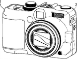
Fig. 1 is as the stereoscopic figure according to the digital camera of the picture pick-up device of the first exemplary embodiment of the present invention when from forward observation.
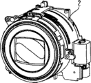
Fig. 2 be illustrate when when the front side is observed according to the stereogram of the image unit the digital camera of the first exemplary embodiment.
Fig. 3 be illustrate when when the back side is observed according to the exploded perspective view of the image unit the digital camera of the first exemplary embodiment.
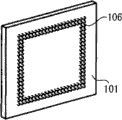
Fig. 4 is the stereogram according to the back side of the photoelectric conversion element package in the image unit of the digital camera of the first exemplary embodiment.
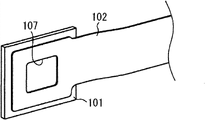
Fig. 5 is the stereogram that illustrates according to the installment state of the photoelectric conversion element package in the image unit of the digital camera of the first exemplary embodiment.
Fig. 6 is the stereogram that the state that is fixed according to the photoelectric conversion element package in the image unit of the digital camera of the first exemplary embodiment and fixed component is shown.
Fig. 7 A to Fig. 7 C shows the structure according to the photoelectric conversion element package in the image unit of the digital camera of the first exemplary embodiment.Fig. 7 A is the vertical view of photoelectric conversion element package, and Fig. 7 B is the end view of photoelectric conversion element package, and Fig. 7 C is the upward view of photoelectric conversion element package.
Fig. 8 is the stereogram that illustrates according to the fixed component in the image unit of the digital camera of the first exemplary embodiment.
Fig. 9 is the stereogram that illustrates according to the assembling completion status of the image unit of the digital camera of the first exemplary embodiment.
Figure 10 be illustrate when when the back side is observed as the exploded perspective view according to the image unit the digital camera of the picture pick-up device of the second exemplary embodiment of the present invention.
Figure 11 is the stereogram that illustrates according to the printed circuit board (PCB) in the image unit of the digital camera of the second exemplary embodiment.
Figure 12 is the stereogram that illustrates according to the installment state of the photoelectric conversion element package in the image unit of the digital camera of the second exemplary embodiment.
Figure 13 is the stereogram that illustrates according to the stationary state of the photoelectric conversion element package in the image unit of the digital camera of the second exemplary embodiment and fixed component.
Figure 14 is the stereogram that illustrates according to the assembling completion status of the image unit of the digital camera of the second exemplary embodiment.
Figure 15 is the stereogram that illustrates according to the photoelectric conversion element package of another structure of the image unit of the first and second exemplary embodiment.
Figure 16 is the exploded perspective view that illustrates when observing from the back side according to the image unit of another structure of the first exemplary embodiment.
Figure 17 is the exploded perspective view that illustrates when observing from the back side according to the image unit of another structure of the second exemplary embodiment.
Embodiment
Describe below with reference to accompanying drawings various exemplary embodiment of the present invention, feature and aspect in detail.
Fig. 1 is as the stereoscopic figure according to the digital camera of the picture pick-up device of the first exemplary embodiment of the present invention when from forward observation.Fig. 2 be illustrate when when the front side is observed according to the stereogram of the image unit the digital camera of the first exemplary embodiment.Fig. 3 be illustrate when when the back side is observed according to the exploded perspective view of the image unit the digital camera of the first exemplary embodiment.Fig. 4 is the stereogram according to the back side of the photoelectric conversion element package in the image unit of the digital camera of the first exemplary embodiment.Fig. 5 is the stereogram that illustrates according to the installment state of the photoelectric conversion element package in the image unit of the digital camera of the first exemplary embodiment.Fig. 6 is the stereogram that illustrates according to the photoelectric conversion element package in the image unit of the digital camera of the first exemplary embodiment and be used for the state that the member of position limitation is fixed.Fig. 7 A to Fig. 7 C shows the structure according to the photoelectric conversion element package in the image unit of the digital camera of the first exemplary embodiment.Fig. 7 A is the vertical view of photoelectric conversion element package, and Fig. 7 B is the end view of photoelectric conversion element package, and Fig. 7 C is the upward view of photoelectric conversion element package.Fig. 8 is the stereogram that illustrates according to the member that is used for position limitation in the image unit of the digital camera of the first exemplary embodiment.Fig. 9 is the stereogram that illustrates according to the assembling completion status of the image unit of the digital camera of the first exemplary embodiment.
In Fig. 1, show the main body of digital camera.Digital camera 1 has image unit 2, and this image unit 2 is so that the front portion of image unit 2 is installed in digital camera 1 via the mode that the opening of the substantial middle section of the front casing that is arranged at digital camera 1 exposes.
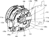
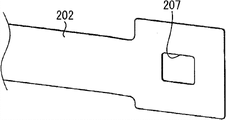
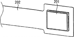
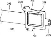
As shown in Figure 3, image unit 2 comprises photoelectric conversion element package 101, photoelectric conversion device module unit 100 and photography barrel unit 104, and this photoelectric conversion device module unit 100 comprises fixed component 103 and as the printed circuit board (PCB) 102 of Wiring member.
Be arranged on installation portion corresponding with roughly back side photoelectric conversion element package 101 the middle position position that is used for installing photoelectric conversion element package 101 of printed circuit board (PCB) 102 with the opening 107 of rectangular shape opening.Heat conduction member 114 is configured in the inboard of opening 107, with the back side of contact photoelectric conversion element package 101.Heat conduction member 114 is by the member with rectangular shape that flexible thermally conductive gel material (heat-conductive gelmaterial) forms.More specifically, heat conduction member 114 is configured to that the two contacts with the back side central portion of photoelectric conversion element package 101 and mainframe 115, and heat conduction member 114 be configured for the leaving thermally conductive pathways of heat of photoelectric conversion element package 101, wherein, mainframe 115 is configured to relative with the back side of photoelectric conversion element package 101 and becomes rack component.
Then, with reference to the structure of Fig. 4, Fig. 5, Fig. 6 and Fig. 7 A to Fig. 7 C Mingguang City's electric transition element modular unit 100 according to assembling process.
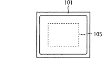
Shown in Fig. 4 and Fig. 7 A to Fig. 7 C, photoelectric conversion element package 101 is constructed to hold the encapsulation of photo-electric conversion element 105.
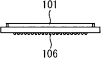
Photoelectric conversion element package 101 is ball grid array (BGA) the type encapsulation with electrode 106, and this electrode 106 is by the back side of making and be formed on photoelectric conversion element package 101 with the soldered ball (solder ball) of grid shape configuration.
At first, as shown in Figure 5, photoelectric conversion element package 101 is installed in printed circuit board (PCB) 102.Printed circuit board (PCB) 102 is formed with pad (land, not shown) in the position corresponding with the electrode 106 of photoelectric conversion element package 101.Photoelectric conversion element package 101 is refluxed weldering and (reflow-mount) is installed in printed circuit board (PCB) 102.In Reflow Soldering was installed, formation was melted and is fixedly secured to the pad that is formed at printed circuit board (PCB) 102 as the soldered ball of the electrode 106 of the splicing ear of photoelectric conversion element package 101, to be electrically connected.
Printed circuit board (PCB) 102 makes BGA type photoelectric conversion element package 101 be installed on this printed circuit board (PCB) 102, thereby, demanding wiring density.In addition, as described below, require printed circuit board (PCB) 102 to be configured to photo-electric conversion element and photographic lens imaging of optical systems are faced the position.Thereby, require the wiring lead section of printed circuit board (PCB) 102 to have high flexibility, to be connected to another circuit board (not shown) from printed circuit board (PCB) 102.
Printed circuit board (PCB) 102 is arranged at the hard and soft property of multilayer printed wiring board (multi-layer rigid flexible printed wiring board).So, in printed circuit board (PCB) 102, require the installation portion that is used for installation photoelectric conversion element package 101 of high wiring density to be configured to rigid portion, require flexible wiring lead division to be configured to flexible part.
As shown in Figure 5, the outermost outer shape of the installation portion that is used for installation photoelectric conversion element package 101 of printed circuit board (PCB) 102 is formed less than the outer shape of photoelectric conversion element package 101.Thus, photoelectric conversion element package 101 is so that the mode that the back side of photoelectric conversion element package 101 exposes from the outside of the profile of printed circuit board (PCB) 102 is installed in printed circuit board (PCB) 102.
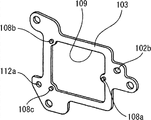
Then, the peripheral part of the photoelectric conversion element package 101 by will being installed on printed circuit board (PCB) 102 is with state location shown in Figure 6 and be adhesively secured to the fixed component 103 that forms the shaped as frame shape and make them integrated.As shown in Figure 8, the plate of the roughly shaped as frame shape that fixed component 103 is configured to be made of metal, and be formed with opening 109 at the central portion of fixed component 103.Fixed component 103 has the jut 108a that forms by semi-stamping (halfblanking) to jut 108c, and these juts 108a is to the position on optical axis direction that jut 108c limits photoelectric conversion element package 101 by the peripheral part butt with the encapsulation back side of photoelectric conversion element package 101.
These juts 108a to 108c is formed on the position that the part in the outside of the outer shape that is positioned at printed circuit board (PCB) 102 on the back side with the photoelectric conversion element package 101 that is in installment state contacts.Thereby jut 108a to 108c directly contacts the back side of photoelectric conversion element package 101.Incidentally, can configure jut more than three.Opening 109 is formed less and larger than the opening 107 of printed circuit board (PCB) 102 than the profile of photoelectric conversion element package 101.
The fixed component 103 of structure is not interfered the heat conduction member 114 that contacts with the back side of photoelectric conversion element package 101 via opening 107 as mentioned above.Simultaneously, the zone that the peripheral part at the back side by photoelectric conversion element package 101 is set and fixed component 103 are overlapping, fixed component 103 can guarantee that the clearance (margin) between photoelectric conversion element package 101 and the fixed component 103 is bonding to carry out.In addition, be easy to make adhesive to flow into this clearance to carry out bonding work from opening 109.
Fixed component 103 in this exemplary embodiment is made of metal, and still, if synthetic resin has enough intensity, then synthetic resin also can be realized the effect that is equal to.
Then, before photoelectric conversion element package 101 and fixed component 103 are fixed, at first the tool using (not shown) determine photoelectric conversion element package 101 with the in-plane of light shaft positive cross on relative position.
Then, by making the jut 108a to 108c that is formed at fixed component 103 and the peripheral part butt at the back side of the photoelectric conversion element package 101 that is positioned determine the relative position of photoelectric conversion element package 101 on optical axis direction.
Then, under this positioning states, adhesive is flowed into the peripheral part and the gap between the fixed component 103 of the photoelectric conversion element package 101 that is positioned via the Outboard Sections of the opening 109 that is formed at fixed component 103 from the outer shape of printed circuit board (PCB) 102.
Here, photoelectric conversion element package 101 is formed under the state that photoelectric conversion element package 101 is installed in printed circuit board (PCB) 102 and can be directly limited by the jut 108a to 108c of fixed component 103 position of photoelectric conversion element package 101 on optical axis direction.
Thereby, make jut 108a to 108c higher than the distance between the back side of the encapsulation back side of photoelectric conversion element package 101 after photoelectric conversion element package 101 is installed in printed circuit board (PCB) 102 and printed circuit board (PCB) 102.Jut 108a to 108c is formed on the position that the peripheral part in the outside of the outer shape that is positioned at printed circuit board (PCB) 102 on the back side with photoelectric conversion element package 101 contacts.Utilize this structure, can in the scope at the back side of photoelectric conversion element package 101, make jut 108a to 108c interval between any two farthest wide.
Thereby, can make the fluctuation minimum of the plan position approach of photo-electric conversion element 105 change into the fluctuation of the height of the jut 108a to 108c that causes owing to processing, thereby can carry out position limitation with high accuracy.
Can with the state at the back side that is installed in printed circuit board (PCB) 102 in photoelectric conversion element package 101 under the height that the identical precision of the precision at the interval between the back side of the back side of photoelectric conversion element package 101 and printed circuit board (PCB) 102 arranges jut 108a to 108c is set.Thereby, 103 gross thickness is minimized.
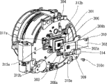
Then, as shown in Figure 9, under the state of the posture of being located integrated photoelectric conversion device module unit 100 by detent mechanism, by screw 110a to 110c this photoelectric conversion device module unit 100 is fastened to photography barrel unit 104.
As shown in Figure 3, detent mechanism makes from the photography barrel unit 104 outstanding 111a of locator protrusions section and 111b and engages with the location hole 112a and the 112b that are formed at fixed component 103 respectively, to position.This detent mechanism with the in-plane location fixed component 103 of the light shaft positive cross of photography barrel unit 104 and photoelectric conversion element package 101 posture (position) with respect to shooting barrel unit 104.
Detent mechanism has a plurality of force application springs (biasing spring) 113a, the 113b etc. (still have force application spring not shown) of the recess that is configured in photography barrel unit 104.A plurality of force application spring 113a, 113b etc. are configured to along optical axis direction fixed component 103 be applied power towards the head of screw of screw 110a to 110c.
By finely tuning the amount of tightening of each screw 110a to 110c, detent mechanism is finely tuned such as fixed component 103 with respect to the position on optical axis direction of photography barrel unit 104 and with respect to the postures such as angle of optical axis.If use the by this way detent mechanism of structure, then can make the photographic lens imaging of optical systems face of the light receiving surface of photo-electric conversion element 105 and the barrel unit 104 of photographing with the high accuracy contraposition.
Then, be incorporated into the main body of digital camera 1 by the photography barrel unit 104 of detent mechanism location posture.Then, the heat conduction member 114 that contacts with the back side of photoelectric conversion element package 101 via the opening 107 of printed circuit board (PCB) 102 is configured to the state that heat conduction member 114 contacts with mainframe 115, and this mainframe 115 is as the radiating component of the heat of the photoelectric conversion element package 101 that leaves.Heat conduction member 114 is rich flexible members, and heat conduction member 114 is configured to have and allows heat conduction member 114 compressed and be sandwiched in photoelectric conversion element package 101 and as the thickness between the mainframe 115 of radiating component.Except mainframe 115, radiating component can comprise a part, the structural elements of the housing of digital camera 1 or be the independent heat radiation special-purpose member that configures of heat radiation.
Thereby when using heat conduction member 114, heat can be loose to mainframe 115 from photoelectric conversion element package 101 via heat conduction member 114, thus, can transmit efficiently and the heat that leaves.For example, when when heat conduction member is configured in situation between fixed component 103 and the mainframe 115 and compares, when heat conduction member 114 is configured between photoelectric conversion element package 101 and the mainframe 115, realized larger radiating effect.
In addition, in digital camera 1, the detent mechanism of photo-electric conversion element 105 is constructed such that photo-electric conversion element 105 is supported by the fixed component in the outside of photoelectric conversion element package 101.
On the contrary, heat conduction member 114 is configured in the substantial middle section at the back side of photoelectric conversion element package 101.If with this formal construction, then can reduce the repulsion of compressed heat conduction member 114 to the impact of photo-electric conversion element 105 with respect to the adjustment state of the inclination of optical axis.
In the digital camera 1 of constructing as mentioned above, can be with hi-Fix photoelectric conversion element package and fixed component.In addition, the heat that leaves of the photo-electric conversion element from digital camera 1 effectively, and do not affect photo-electric conversion element with respect to the tilt adjustments of optical axis orthogonal plane, thus can suppress the rising of the temperature of photo-electric conversion element.
In above-mentioned the first exemplary embodiment, photoelectric conversion element package 101 is the encapsulation of ball grid array (BGA) type, and still, photoelectric conversion element package 101 also can be configured to the encapsulation of grid array (LGA) type.Replace the encapsulation of back electrode type, although electrode is formed on the limit of side, the structure of the first exemplary embodiment also goes for the encapsulation that has the type of electrode on two relative limits.
In the first exemplary embodiment, heat conduction member 114 directly is disposed at the back side of photoelectric conversion element package 101, but, as shown in figure 15, also can use heat transmission electrode 306 (radiating part) as splicing ear to be arranged at the encapsulation of central portion at the back side of photoelectric conversion element package.
In this case, as shown in figure 16, expose the pad (not shown) as the Copper Foil of cooling pad and be arranged on the relative position of electrode printed circuit board (PCB) 302 and photoelectric conversion element package 301 306.The heat transmission electrode 306 that is connected to as splicing ear is filled up in Copper Foil exposure as cooling pad.More specifically, when photoelectric conversion element package 301 is refluxed weldering when being installed on printed circuit board (PCB) 302, the soldered ball that forms heat transmission electrode 306 is melted and is fixedly secured to the Copper Foil that is formed at printed circuit board (PCB) 302 and exposes pad, to connect.
Then, with reference to Figure 10 to Figure 14 the second exemplary embodiment of the present invention is described.
Figure 10 be illustrate when when the back side is observed as the exploded perspective view of the image unit the digital camera of second embodiment of the invention picture pick-up device.Figure 11 is the stereogram that illustrates according to the printed circuit board (PCB) in the image unit of the digital camera of the second exemplary embodiment.Figure 12 is the stereogram that illustrates according to the installment state of the photoelectric conversion element package in the image unit of the digital camera of the second exemplary embodiment.Figure 13 is the stereogram that illustrates according to the stationary state of the photoelectric conversion element package in the image unit of the digital camera of the second exemplary embodiment and fixed component.Figure 14 is the stereogram that illustrates according to the assembling completion status of the image unit of the digital camera of the second exemplary embodiment.
Be installed in according to the image unit in the digital camera of the second exemplary embodiment and comprise photoelectric conversion device module unit 200 and photography barrel unit 204.Photoelectric conversion device module unit 200 comprises photoelectric conversion element package 201, printed circuit board (PCB) 202 and fixed component 203.
The structure of photoelectric conversion device module unit 200 then, is described according to assembling process with reference to Figure 11, Figure 12 and Figure 13.
As shown in figure 11, the same with above-mentioned the first exemplary embodiment, before photoelectric conversion element package 201 was configured to installation state shown in Figure 12, photoelectric conversion element package 201 was refluxed the opening that weldering is installed on the installation portion that forms printed circuit board (PCB) 202.
Printed circuit board (PCB) 202 according to the second exemplary embodiment has the flexibility identical with the first exemplary embodiment, thereby is configured to rigid flexible printed circuit board.
As shown in figure 13, the photoelectric conversion element package 201 that is installed on printed circuit board (PCB) 202 is fixed by fixed component 203.The plate that fixed component 203 is configured to be made of metal.Opening 209 is formed on the central portion of fixed component 203.
Be used for the fixedly fixing means of photoelectric conversion element package 201 and fixed component 203, the tool using (not shown) is determined the relative position of the each party in photoelectric conversion element package 201 and the fixed component 203.Then, under this positioning states, adhesive is flowed into be formed at the opening 209 of fixed component 203 and by in the gap between the package wall of the photoelectric conversion element package 201 of tool positioned in opening 209, with fixedly photoelectric conversion element package 201 and fixed component 203.
Then, as shown in figure 14, by screw 210a to 210c photoelectric conversion device module unit 200 is fastened to photography barrel unit 204.
According to the photoelectric conversion device module unit 200 of the second exemplary embodiment comprise fine setting photography barrel unit 204 on optical axis direction the position and with respect to the mechanism of the angle of optical axis.In addition, photoelectric conversion device module unit 200 comprises the structure that heat conduction member 214 is contacted with mainframe 215.
According to the structure of the photoelectric conversion device module unit 200 in above-mentioned the second exemplary embodiment, can be by making heat conduction member 214 distortion with hi-Fix photoelectric conversion element package and fixed component.In addition, utilize the structure of photoelectric conversion device module unit 200 can effectively leave from the heat of photo-electric conversion element, and can not affect photo-electric conversion element with respect to the tilt adjustments of optical axis orthogonal plane, thereby can suppress the rising of the temperature of photo-electric conversion element.
In the second exemplary embodiment, heat conduction member 214 directly is configured in the back side of photoelectric conversion element package 201, but, as shown in figure 15, also can use heat transmission electrode (radiating part) as splicing ear to be arranged on the encapsulation of central portion at the back side of photoelectric conversion element package.
In this case, as shown in figure 17, expose the pad (not shown) as the Copper Foil of cooling pad and be arranged on the relative position of electrode printed circuit board (PCB) 402 and photoelectric conversion element package 301 306.The heat transmission electrode 306 that is connected to as splicing ear is filled up in Copper Foil exposure as cooling pad.More specifically, when photoelectric conversion element package 301 is refluxed weldering when being installed on printed circuit board (PCB) 402, the soldered ball that forms heat transmission electrode 306 is melted and is fixedly secured to the Copper Foil that is formed at printed circuit board (PCB) 402 and exposes pad, to connect.Backside heat pad 402a is formed on the back side of printed circuit board (PCB) 402, and exposes pad and backside heat pad 402a by the through hole connection copper foil of printed circuit board (PCB) 402 inside.Even when heat conduction member 414 is configured to contact with the backside heat pad 402a that is connected to Copper Foil and exposes pad, also can realize and the similar effect of the effect of the second exemplary embodiment.
Although with reference to exemplary embodiment the present invention has been described, has been to be understood that to the invention is not restricted to disclosed exemplary embodiment.The scope of claims should give the most wide in range explanation, to comprise all modification, equivalent structure and function.
Claims (11)
1. picture pick-up device, it comprises:
Photoelectric conversion element package;
Rack component, it is configured in the position relative with the back side of described photoelectric conversion element package;
Wiring member, it is electrically connected to described photoelectric conversion element package, wherein, described Wiring member has the first opening of the back exposure that makes described photoelectric conversion element package, and described Wiring member is configured between the back side and described rack component of described photoelectric conversion element package;
Fixed component, it is configured to described photoelectric conversion element package is fixed, and wherein, described fixed component has second opening larger than described first opening of described Wiring member; And
Heat conduction member, it is configured to directly contact with the back side of described the second opening with described rack component and described photoelectric conversion element package via described the first opening, wherein, described heat conduction member is compressed and be clipped between described photoelectric conversion element package and the described rack component.
2. picture pick-up device according to claim 1, it is characterized in that, described fixed component is adhesively secured to the back side of described photoelectric conversion element package, wherein, described fixed component has jut, and described jut is configured to the position by contacting to limit described photoelectric conversion element package with the back side of described photoelectric conversion element package.
3. picture pick-up device according to claim 2 is characterized in that, described jut is formed on the position that part described fixed component and the described Wiring member of being positioned at of the back side described photoelectric conversion element package the outside contacts.
4. picture pick-up device according to claim 1 is characterized in that, the described photoelectric conversion element package of described the second aperture efficiency is large, and described fixed component is adhesively secured to the package wall of described photoelectric conversion element package,
Wherein, described Wiring member covers the back side of described photoelectric conversion element package and at least a portion of described fixed component.
5. picture pick-up device according to claim 1 is characterized in that, described heat conduction member comprises the thermally conductive gel material.
6. picture pick-up device, it comprises:
Photoelectric conversion element package is formed with radiating part at the back side of described photoelectric conversion element package;
Rack component, it is configured in the position relative with the back side of described photoelectric conversion element package;
Wiring member, it has the cooling pad that contacts with the described radiating part of described photoelectric conversion element package, described Wiring member is configured between the back side and described rack component of described photoelectric conversion element package, and described Wiring member is electrically connected to described photoelectric conversion element package;
Fixed component, it is configured to described photoelectric conversion element package is fixed, and wherein, described fixed component has the opening larger than heat conduction member; And
Described heat conduction member, it is configured to directly contact with described rack component with the back side of the described cooling pad of described Wiring member via described opening, and wherein, described heat conduction member is compressed and be clipped between the back side and described rack component of described cooling pad.
7. picture pick-up device according to claim 6 is characterized in that, forms the backside heat pad at the back side of described Wiring member, connects described cooling pad and described backside heat pad by the through hole that is formed at described Wiring member.
8. picture pick-up device according to claim 6 is characterized in that,
Described fixed component has jut, and described jut is configured to fix described photoelectric conversion element package by contacting with the back side of described photoelectric conversion element package, and
Described fixed component is adhesively secured to the back side of described photoelectric conversion element package.
9. picture pick-up device according to claim 8 is characterized in that, described jut is formed on the position that part described fixed component and the described Wiring member of being positioned at of the back side described photoelectric conversion element package the outside contacts.
10. picture pick-up device according to claim 6 is characterized in that, the described photoelectric conversion element package of described aperture efficiency is large, and described fixed component is adhesively secured to the package wall of described photoelectric conversion element package,
Wherein, described Wiring member covers the back side of described photoelectric conversion element package and at least a portion of described fixed component.
11. picture pick-up device according to claim 6 is characterized in that, described heat conduction member comprises the thermally conductive gel material.
Applications Claiming Priority (2)
| Application Number | Priority Date | Filing Date | Title |
|---|---|---|---|
| JP2009079209A JP5225171B2 (en) | 2009-03-27 | 2009-03-27 | Imaging device |
| JP2009-079209 | 2009-03-27 |
Publications (2)
| Publication Number | Publication Date |
|---|---|
| CN101848326A CN101848326A (en) | 2010-09-29 |
| CN101848326B true CN101848326B (en) | 2013-01-09 |
Family
ID=42772769
Family Applications (1)
| Application Number | Title | Priority Date | Filing Date |
|---|---|---|---|
| CN201010141137.0A Expired - Fee Related CN101848326B (en) | 2009-03-27 | 2010-03-25 | Imaging apparatus |
Country Status (3)
| Country | Link |
|---|---|
| US (1) | US8493503B2 (en) |
| JP (1) | JP5225171B2 (en) |
| CN (1) | CN101848326B (en) |
Families Citing this family (7)
| Publication number | Priority date | Publication date | Assignee | Title |
|---|---|---|---|---|
| WO2010007745A1 (en) * | 2008-07-18 | 2010-01-21 | パナソニック株式会社 | Imaging device |
| JP2012032704A (en) * | 2010-08-02 | 2012-02-16 | Canon Inc | Imaging apparatus |
| KR20130127841A (en) * | 2012-05-15 | 2013-11-25 | 삼성전자주식회사 | Photographing apparatus and manufacturing method thereof |
| JP6588243B2 (en) * | 2015-06-09 | 2019-10-09 | オリンパス株式会社 | Cooling structure of photoelectric conversion element |
| GB2561103A (en) | 2015-10-30 | 2018-10-03 | Canon Kk | Electronic apparatus |
| GB2559515B (en) | 2015-10-30 | 2021-11-10 | Canon Kk | Electronic device |
| JP7118853B2 (en) * | 2018-10-16 | 2022-08-16 | キヤノン株式会社 | Imaging unit |
Citations (4)
| Publication number | Priority date | Publication date | Assignee | Title |
|---|---|---|---|---|
| CN101261983A (en) * | 2007-03-07 | 2008-09-10 | 奥林巴斯映像株式会社 | Semiconductor device with image pick-up element |
| CN101299433A (en) * | 2007-05-01 | 2008-11-05 | 奥林巴斯映像株式会社 | Image pickup member module, lens unit using the same and portable electronic device |
| CN101374201A (en) * | 2007-08-24 | 2009-02-25 | 佳能株式会社 | Imaging apparatus and photoelectric conversion element package retaining unit |
| US7499635B2 (en) * | 2004-09-10 | 2009-03-03 | Konica Minolta Photo Imaging, Inc. | Image pickup apparatus incorporating shake correction |
Family Cites Families (14)
| Publication number | Priority date | Publication date | Assignee | Title |
|---|---|---|---|---|
| US6654064B2 (en) * | 1997-05-23 | 2003-11-25 | Canon Kabushiki Kaisha | Image pickup device incorporating a position defining member |
| JP4046837B2 (en) | 1998-03-11 | 2008-02-13 | キヤノン株式会社 | Imaging device |
| US6956615B2 (en) * | 2000-01-28 | 2005-10-18 | Pentax Corporation | Structure for mounting a solid-state imaging device |
| JP4169938B2 (en) * | 2000-01-28 | 2008-10-22 | Hoya株式会社 | Solid-state image sensor holding block and solid-state image sensor mounting structure |
| JP3613193B2 (en) * | 2001-03-30 | 2005-01-26 | 三菱電機株式会社 | Imaging device |
| JP4083521B2 (en) * | 2001-10-29 | 2008-04-30 | オリンパス株式会社 | Imaging device |
| JP2006086752A (en) * | 2004-09-15 | 2006-03-30 | Fuji Photo Film Co Ltd | Lens interchangeable camera integral with imaging element and interchangeable lens unit integral with imaging element |
| JP2006191465A (en) * | 2005-01-07 | 2006-07-20 | Seiko Instruments Inc | Electronic apparatus |
| JP2006295714A (en) * | 2005-04-13 | 2006-10-26 | Olympus Corp | Imaging apparatus |
| JP2007166006A (en) * | 2005-12-09 | 2007-06-28 | Sony Corp | Imaging apparatus |
| JP2008271487A (en) * | 2007-03-29 | 2008-11-06 | Olympus Imaging Corp | Imaging element module, lens unit using the imaging element module and portable electronic device |
| CN101369592A (en) * | 2007-08-14 | 2009-02-18 | 鸿富锦精密工业(深圳)有限公司 | Image sensor |
| TW200951616A (en) * | 2008-06-05 | 2009-12-16 | Asia Optical Co Inc | Image sensing module |
| JP4770854B2 (en) * | 2008-03-19 | 2011-09-14 | カシオ計算機株式会社 | Digital camera |
-
2009
- 2009-03-27 JP JP2009079209A patent/JP5225171B2/en not_active Expired - Fee Related
-
2010
- 2010-03-25 CN CN201010141137.0A patent/CN101848326B/en not_active Expired - Fee Related
- 2010-03-25 US US12/731,519 patent/US8493503B2/en not_active Expired - Fee Related
Patent Citations (4)
| Publication number | Priority date | Publication date | Assignee | Title |
|---|---|---|---|---|
| US7499635B2 (en) * | 2004-09-10 | 2009-03-03 | Konica Minolta Photo Imaging, Inc. | Image pickup apparatus incorporating shake correction |
| CN101261983A (en) * | 2007-03-07 | 2008-09-10 | 奥林巴斯映像株式会社 | Semiconductor device with image pick-up element |
| CN101299433A (en) * | 2007-05-01 | 2008-11-05 | 奥林巴斯映像株式会社 | Image pickup member module, lens unit using the same and portable electronic device |
| CN101374201A (en) * | 2007-08-24 | 2009-02-25 | 佳能株式会社 | Imaging apparatus and photoelectric conversion element package retaining unit |
Also Published As
| Publication number | Publication date |
|---|---|
| US20100245662A1 (en) | 2010-09-30 |
| JP2010233015A (en) | 2010-10-14 |
| US8493503B2 (en) | 2013-07-23 |
| JP5225171B2 (en) | 2013-07-03 |
| CN101848326A (en) | 2010-09-29 |
Similar Documents
| Publication | Publication Date | Title |
|---|---|---|
| CN101848326B (en) | Imaging apparatus | |
| JP6597729B2 (en) | Imaging unit and imaging apparatus | |
| US7190404B2 (en) | Solid state imaging apparatus | |
| US7515817B2 (en) | Camera module | |
| CN100409668C (en) | Image pickup unit and image pickup apparatus | |
| JP2007049369A (en) | Holding structure of image sensor package, and lens unit | |
| KR20070047721A (en) | Image pickup device mounting structure | |
| JPWO2006088051A1 (en) | The camera module | |
| JPWO2008132979A1 (en) | Imaging device manufacturing method and imaging device | |
| US20210051251A1 (en) | Camera device and mobile terminal having same | |
| JP5117967B2 (en) | Electronic equipment and electronic equipment with imaging function | |
| JP5203318B2 (en) | Imaging module and manufacturing method thereof | |
| JP2015023343A (en) | Imaging apparatus | |
| JP2016019005A (en) | Imaging device | |
| CN100422844C (en) | Optical equipment having image pickup element | |
| JP7078151B2 (en) | Imaging unit and imaging device | |
| JP6675241B2 (en) | Imaging device | |
| JP6849016B2 (en) | Imaging unit and imaging device | |
| JP2003303944A (en) | Manufacturing method of solid-state image pickup device | |
| CN214544470U (en) | Periscopic camera module and electronic equipment | |
| JP2018189667A (en) | Imaging apparatus | |
| US20230199289A1 (en) | Image pickup apparatus | |
| JP6547799B2 (en) | Imaging unit and imaging apparatus | |
| US10136039B2 (en) | Image pickup apparatus capable of preventing thermal deformation of a fixing member fixed to image pickup device package | |
| JP3857848B2 (en) | Position adjustment mechanism of solid-state image sensor |
Legal Events
| Date | Code | Title | Description |
|---|---|---|---|
| C06 | Publication | ||
| PB01 | Publication | ||
| C10 | Entry into substantive examination | ||
| SE01 | Entry into force of request for substantive examination | ||
| C14 | Grant of patent or utility model | ||
| GR01 | Patent grant | ||
| CF01 | Termination of patent right due to non-payment of annual fee |
Granted publication date: 20130109 Termination date: 20200325 |
|
| CF01 | Termination of patent right due to non-payment of annual fee |