JP6032911B2 - Photoelectric conversion element and manufacturing method thereof - Google Patents
Photoelectric conversion element and manufacturing method thereof Download PDFInfo
- Publication number
- JP6032911B2 JP6032911B2 JP2012066454A JP2012066454A JP6032911B2 JP 6032911 B2 JP6032911 B2 JP 6032911B2 JP 2012066454 A JP2012066454 A JP 2012066454A JP 2012066454 A JP2012066454 A JP 2012066454A JP 6032911 B2 JP6032911 B2 JP 6032911B2
- Authority
- JP
- Japan
- Prior art keywords
- amorphous
- type
- semiconductor substrate
- amorphous film
- single crystal
- Prior art date
- Legal status (The legal status is an assumption and is not a legal conclusion. Google has not performed a legal analysis and makes no representation as to the accuracy of the status listed.)
- Active
Links
Images


Classifications
-
- Y—GENERAL TAGGING OF NEW TECHNOLOGICAL DEVELOPMENTS; GENERAL TAGGING OF CROSS-SECTIONAL TECHNOLOGIES SPANNING OVER SEVERAL SECTIONS OF THE IPC; TECHNICAL SUBJECTS COVERED BY FORMER USPC CROSS-REFERENCE ART COLLECTIONS [XRACs] AND DIGESTS
- Y02—TECHNOLOGIES OR APPLICATIONS FOR MITIGATION OR ADAPTATION AGAINST CLIMATE CHANGE
- Y02E—REDUCTION OF GREENHOUSE GAS [GHG] EMISSIONS, RELATED TO ENERGY GENERATION, TRANSMISSION OR DISTRIBUTION
- Y02E10/00—Energy generation through renewable energy sources
- Y02E10/50—Photovoltaic [PV] energy
Description
この発明は、光電変換素子およびその製造方法に関するものである。 The present invention relates to a photoelectric conversion element and a manufacturing method thereof.
太陽光エネルギを電気エネルギに直接変換する太陽電池は、近年、特に、地球環境問題の観点から、次世代のエネルギ源としての期待が急激に高まっている。太陽電池としては、化合物半導体または有機材料を用いたものなど様々な種類があるが、現在、主流となっているのは、シリコン結晶を用いたものである。 In recent years, a solar cell that directly converts solar energy into electric energy has been rapidly expected as a next-generation energy source particularly from the viewpoint of global environmental problems. There are various types of solar cells, such as those using compound semiconductors or organic materials, but the mainstream is currently using silicon crystals.
現在、最も多く製造および販売されている太陽電池は、太陽光が入射する側の面である受光面と、受光面の反対側である裏面とに電極が形成された構造のものである。 Currently, the most manufactured and sold solar cells have a structure in which electrodes are formed on a light receiving surface that is a surface on which sunlight is incident and a back surface that is the opposite side of the light receiving surface.
しかしながら、受光面に電極を形成した場合、電極における光の反射、吸収があることから、形成された電極の面積分だけ入射する太陽光が減少するので、裏面にのみ電極を形成した太陽電池が開発されている。 However, when an electrode is formed on the light receiving surface, since there is reflection and absorption of light at the electrode, sunlight incident on the area of the formed electrode is reduced, so a solar cell having an electrode formed only on the back surface Has been developed.
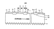
図11は、特許文献1に開示されている裏面にのみ電極を形成した従来の太陽電池を表す平面図である。また、図12は、図11に示す線XII−XII間における太陽電池の断面である。
FIG. 11 is a plan view showing a conventional solar cell in which electrodes are formed only on the back surface disclosed in
太陽電池300の裏面には、n側電極140n及びp側電極140pが形成されている。また、半導体基板111の裏面には、in接合120、ip接合130が形成されている。in接合120は、i型アモルファスシリコン層120iとn型アモルファスシリコン層120nとによって構成されている。また、ip接合130は、i型アモルファスシリコン層130iとp型アモルファスシリコン層130pとによって構成されている。n型アモルファスシリコン層120nとp型アモルファスシリコン層130pとは、i型アモルファスシリコン層130iによって電気的に分離されている。120fは、斜面である。
On the back surface of the
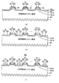
図13は、特許文献1に開示されている太陽電池の製造方法の一例を示す工程図である。図13に示すように、模式的断面図を参照して太陽電池300の製造方法を説明する。
FIG. 13 is a process diagram showing an example of a method for manufacturing a solar cell disclosed in
まず、図13(a)に示すように、n型単結晶シリコン基板である半導体基板111の裏面上に、CVD法を用いて、i型アモルファスシリコン層120iとn型アモルファスシリコン層120nを順次形成する。これによって、in接合120が形成される。
First, as shown in FIG. 13A, an i-type
次に、図13(b)に示すように、n型アモルファスシリコン層120n上に、CVD法を用いて、被覆層150を形成する。被覆層150としては、例えば、窒化シリコンや酸化シリコンなどを用いることができる。
Next, as shown in FIG. 13B, a
次に、図13(c)に示すように、フォトリソグラフィ法によって、被覆層150の一部を所定間隔で第1方向に沿って除去する。これによって、第1方向に沿ってそれぞれ延びる複数の第1溝150gが形成される。
Next, as shown in FIG. 13C, a part of the
次に、図13(d)に示すように、被覆層150をマスクとし、アルカリ水溶液を用いた等方性エッチング法によって、i型アモルファスシリコン層120iとn型アモルファスシリコン層120nとの一部を所定間隔で第1方向に沿って除去する。これによって、第1方向に沿ってそれぞれ延びる複数本の第2溝120gが形成される。第2溝120gは、第1溝150gから半導体基板111側に延び、半導体基板111まで達するように形成される。
Next, as shown in FIG. 13D, a part of the i-type
ここで、第2溝120gを形成する工程では、n型アモルファスシリコン層120nのうち、被覆層150の第1方向と略直交する第2方向における一端部と半導体基板111との間に設けられた部分をも除去する。すなわち、被覆層150の下に設けられたn型アモルファスシリコン層120nを抉るように除去する。被覆層150の下でエッチングを等方的に進めることによって、in接合120に斜面120fが形成される。
Here, in the step of forming the
次に、図13(e)に示すように、第2溝120gの底面上及び側面上に、CVD法を用いて、i型アモルファスシリコン層130iとp型アモルファスシリコン層130pとを順次形成する。これによって、ip接合130が形成される。被覆層150の下部にも回り込むようにi型アモルファスシリコン層130i及びp型アモルファスシリコン層130pを形成することによって、in接合120の斜面120fは、ip接合130のi型アモルファスシリコン層130iによって覆われる。n型アモルファスシリコン層120nとp型アモルファスシリコン層130pとは、i型アモルファスシリコン層130iによって電気的に分離される。
Next, as shown in FIG. 13E, an i-type
次に、図13(f)に示すように、エッチング法によって、被覆層150を全て除去する。これによって、ip接合130とn型アモルファスシリコン層120nとが露出される。なお、このときp型アモルファスシリコン層130pの端部は、i型アモルファスシリコン層130iによって覆われており、p型アモルファスシリコン層130pの中央部は、露出される。また、本工程において、被覆層150の表面に形成されたi型アモルファスシリコン層130iとp型アモルファスシリコン層130pとは、被覆層150とともに除去される。
Next, as shown in FIG. 13F, the
次に、スパッタリング法を用いて、n型アモルファスシリコン層120n上及びp型アモルファスシリコン層130p上に、第1方向に沿って、ITO(indium tin oxide)層である透明電極層を形成する。続いて、印刷法や塗布法などを用いて、透明電極層上に銀ペーストである導電層を形成する。このようにして、太陽電池300が製造される。
Next, a transparent electrode layer, which is an indium tin oxide (ITO) layer, is formed along the first direction on the n-type
しかしながら、特許文献1においては、裏面にpn接合をパターン形成するため、pn接合形成時には最低2回製膜をしなければならず、2回目の製膜時は1回目の製膜によるプラズマダメージ層上に製膜することになる。それにより、2回目の製膜箇所の界面パッシベーションが十分になされず、太陽電池特性の低下を招くという問題がある。
However, in
そこで、この発明の実施の形態によれば、2回目の製膜箇所の界面パッシベーション性を低下させない光電変換素子を提供する。 Therefore, according to the embodiment of the present invention, a photoelectric conversion element that does not deteriorate the interface passivation property of the second film forming portion is provided.
また、この発明の実施の形態によれば、2回目の製膜箇所の界面パッシベーション性を低下させない光電変換素子の製造方法を提供する。 Moreover, according to this Embodiment, the manufacturing method of the photoelectric conversion element which does not reduce the interface passivation property of the 2nd film forming location is provided.
この発明の実施の形態によれば、光電変換素子は、半導体基板と、第1および第2の非晶質膜とを備える。半導体基板は、第1の導電型を有する単結晶シリコンからなる。第1の非晶質膜は、半導体基板の一方の表面に接して設けられ、第1の導電型と反対の第2の導電型を有する第1の不純物層を少なくとも含む。第2の非晶質膜は、半導体基板の面内方向において第1の非晶質膜に隣接して半導体基板の一方の表面に接して設けられ、第1の導電型を有する第2の不純物層を少なくとも含む。そして、第1および第2の非晶質膜の一方と半導体基板との界面は、半導体基板の厚み方向において、第1および第2の非晶質膜の他方と半導体基板との界面と異なる位置に存在する。 According to the embodiment of the present invention, the photoelectric conversion element includes a semiconductor substrate and first and second amorphous films. The semiconductor substrate is made of single crystal silicon having the first conductivity type. The first amorphous film is provided in contact with one surface of the semiconductor substrate and includes at least a first impurity layer having a second conductivity type opposite to the first conductivity type. The second amorphous film is provided in contact with one surface of the semiconductor substrate adjacent to the first amorphous film in the in-plane direction of the semiconductor substrate, and the second impurity having the first conductivity type Including at least a layer. The interface between one of the first and second amorphous films and the semiconductor substrate is different from the interface between the other of the first and second amorphous films and the semiconductor substrate in the thickness direction of the semiconductor substrate. Exists.
また、この発明の実施の形態によれば、光電変換素子の製造方法は、第1の導電型を有する単結晶シリコンからなる半導体基板の一方の表面に接して、第1の導電型と反対の第2の導電型を有する第1の不純物層を少なくとも含む第1の非晶質膜と、前記第1の導電型を有する第2の不純物層を少なくとも含む第2の非晶質膜とのうち、一方の非晶質膜を形成する第1の工程と、半導体基板の面内方向における一方の非晶質膜の一部分と、該一部分に接する半導体基板の一部分とを除去する第2の工程と、一方の非晶質膜の残部上に被覆層を形成する第3の工程と、半導体基板の一方の表面および被覆層上に第1および第2の非晶質膜の他方の非晶質膜を形成する第4の工程と、被覆層を除去する第5の工程とを備える。 According to the embodiment of the present invention, the method for manufacturing a photoelectric conversion element is in contact with one surface of a semiconductor substrate made of single crystal silicon having the first conductivity type and is opposite to the first conductivity type. A first amorphous film including at least a first impurity layer having a second conductivity type, and a second amorphous film including at least a second impurity layer having the first conductivity type. A first step of forming one of the amorphous films; a second step of removing a portion of the one amorphous film in the in-plane direction of the semiconductor substrate and a portion of the semiconductor substrate in contact with the portion; A third step of forming a coating layer on the remaining portion of the one amorphous film, and the other amorphous film of the first and second amorphous films on one surface of the semiconductor substrate and the coating layer And a fourth step of removing the coating layer.
この発明の実施の形態による光電変換素子においては、第1および第2の非晶質膜の一方と半導体基板との界面は、半導体基板の厚み方向において、第1および第2の非晶質膜の他方と半導体基板との界面と異なる位置に存在する。その結果、第1および第2の非晶質膜の両方は、プラズマダメージが無い半導体基板に接して形成され、キャリア(電子および正孔)の伝導特性が向上する。 In the photoelectric conversion element according to the embodiment of the present invention, the interface between one of the first and second amorphous films and the semiconductor substrate is the first and second amorphous films in the thickness direction of the semiconductor substrate. It exists in a position different from the interface between the other of the semiconductor substrate and the semiconductor substrate. As a result, both the first and second amorphous films are formed in contact with the semiconductor substrate free from plasma damage, and the conduction characteristics of carriers (electrons and holes) are improved.
従って、光電変換素子の変換効率を向上できる。 Therefore, the conversion efficiency of the photoelectric conversion element can be improved.
また、この発明の実施の形態による光電変換素子の製造方法においては、第1および第2の非晶質膜の一方の非晶質膜が半導体基板上に形成され、該一方の非晶質膜の一部分およびその一部分に接する半導体基板の一部分が除去された位置に第1および第2の非晶質膜の他方の非晶質膜が形成される。その結果、第1および第2の非晶質膜の両方は、プラズマダメージが無い半導体基板に接して形成され、キャリア(電子および正孔)の伝導特性が向上する。 In the method of manufacturing a photoelectric conversion element according to the embodiment of the present invention, one of the first and second amorphous films is formed on a semiconductor substrate, and the one amorphous film The other amorphous film of the first and second amorphous films is formed at a position where a part of the semiconductor substrate and a part of the semiconductor substrate in contact with the part are removed. As a result, both the first and second amorphous films are formed in contact with the semiconductor substrate free from plasma damage, and the conduction characteristics of carriers (electrons and holes) are improved.
従って、光電変換素子の変換効率を向上できる。 Therefore, the conversion efficiency of the photoelectric conversion element can be improved.
本発明の実施の形態について図面を参照しながら詳細に説明する。なお、図中同一または相当部分には同一符号を付してその説明は繰返さない。 Embodiments of the present invention will be described in detail with reference to the drawings. In the drawings, the same or corresponding parts are denoted by the same reference numerals and description thereof will not be repeated.
この明細書において、「非晶質相」とは、シリコン(Si)原子等がランダムに配列された状態を言う。また、アモルファスシリコンを「a−Si」と表記するが、この表記は、実際には、水素(H)原子が含まれていることを意味する。アモルファスシリコンカーバイド(a−SiC)、アモルファスシリコンオキサイド(a−SiO)、アモルファスシリコンナイトライド(a−SiN)、アモルファスシリコンカーボンナイトライド(a−SiCN)、アモルファスシリコンゲルマニウム(a−SiGe)およびアモルファスゲルマニウム(a−Ge)についても、同様に、H原子が含まれていることを意味する。 In this specification, the “amorphous phase” refers to a state in which silicon (Si) atoms and the like are randomly arranged. Moreover, although amorphous silicon is described as “a-Si”, this notation actually means that hydrogen (H) atoms are included. Amorphous silicon carbide (a-SiC), amorphous silicon oxide (a-SiO), amorphous silicon nitride (a-SiN), amorphous silicon carbon nitride (a-SiCN), amorphous silicon germanium (a-SiGe) and amorphous germanium Similarly, (a-Ge) means that an H atom is contained.
[実施の形態1]
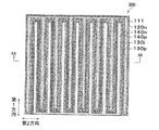
図1は、この発明の実施の形態1による光電変換素子の平面図である。また、図2は、図1に示す線II−II間における光電変換素子の断面図である。なお、図1は、光電変換素子の裏面側の平面図である。図1,2を参照して、この発明の実施の形態1による光電変換素子100は、n型単結晶シリコン基板1と、反射防止膜2と、非晶質膜11〜1m(mは2以上の整数)と、非晶質膜21〜2m−1と、電極3,4とを備える。
[Embodiment 1]
FIG. 1 is a plan view of a photoelectric conversion element according to
n型単結晶シリコン基板1は、例えば、(100)の面方位および0.1〜1.0Ω・cmの比抵抗を有する。また、n型単結晶シリコン基板1は、例えば、100〜300μmの厚みを有し、好ましくは、100〜200μmの厚みを有する。更に、n型単結晶シリコン基板1は、光入射側の表面(反射防止膜2が形成された表面)にテクスチャ構造を有する。更に、n型単結晶シリコン基板1は、裏面(反射防止膜2が形成された面と反対側の表面)において、矩形の凸部1Aと凹部1Bとを有する。凸部1Aの高さ(=凹部1Bの深さ)は、20nm〜5μmである。
The n-type single
反射防止膜2は、例えば、窒化シリコン膜からなり、n型単結晶シリコン基板1の光入射側の表面に接して設けられる。そして、反射防止膜2は、例えば、100nmの膜厚を有する。
The
非晶質膜11〜1mの各々は、非晶質相からなり、n型単結晶シリコン基板1の光入射側と反対側の表面に接して設けられる。より具体的には、非晶質膜11〜1mの各々は、n型単結晶シリコン基板1の凸部1Aに接して設けられる。そして、非晶質膜11〜1mは、n型単結晶シリコン基板1の面内方向において所望の間隔で配置される。
Each of the
非晶質膜21〜2m−1は、非晶質相からなり、n型単結晶シリコン基板1の光入射側と反対側の表面に接して設けられる。より具体的には、非晶質膜21〜2m−1の各々は、n型単結晶シリコン基板1の凹部1Bに接して設けられる。そして、非晶質膜21〜2m−1は、n型単結晶シリコン基板1の面内方向において所望の間隔で配置される。
Amorphous films 21-2m-1 are made of an amorphous phase, and are provided in contact with the surface of n-type single
電極3は、非晶質膜11〜1mに接して設けられる。電極4は、非晶質膜21〜2m−1に接して設けられる。そして、電極3,4は、櫛形の平面形状を有し、交互に噛み合うように配置される。また、電極3,4の各々は、例えば、銀(Ag)からなる。その結果、電極3,4は、それぞれ、非晶質膜11〜1mおよび非晶質膜21〜2m−1とオーミックコンタクトを形成する。
The
図3は、図2に示す非晶質膜11,21の拡大図である。図3を参照して、非晶質膜11は、非晶質膜11A,11Bのいずれかからなり、非晶質膜21は、非晶質膜21A,21Bのいずれかからなる。そして、非晶質膜11A,11Bと非晶質膜21A,21Bとの組み合わせは、図3の(a)〜(d)に示すように4通りである。
FIG. 3 is an enlarged view of the
非晶質膜11Aは、ノンドープ層101と、p型不純物層102とからなる。ノンドープ層101は、n型単結晶シリコン基板1の凸部1Aに接して配置される。p型不純物層102は、ノンドープ層101に接して配置される。
The
ノンドープ層101は、i型の導電型を有し、例えば、i型a−Siからなり、膜厚は、例えば、5〜10nmである。p型不純物層102は、p型の導電型を有し、例えば、p型a−Siからなり、例えば、5×1019cm−3のボロン(B)を含む。また、p型不純物層102は、5〜10nmの膜厚を有する。従って、非晶質膜11Aは、全体で10〜20nmの膜厚を有する。
The
非晶質膜21Aは、ノンドープ層201と、n型不純物層202とからなる。ノンドープ層201は、n型単結晶シリコン基板1の凹部1Bに接して配置される。n型不純物層202は、ノンドープ層201に接して配置される。
The
ノンドープ層201は、i型の導電型を有し、例えば、i型a−Siからなり、膜厚は、例えば、5nm〜10nmである。n型不純物層202は、n型の導電型を有し、例えば、n型a−Siからなり、例えば、5×1019cm−3のリン(P)を含む。また、n型不純物層202は、5nm〜10nmの膜厚を有する。従って、非晶質膜21Aは、全体で10nm〜20nmの膜厚を有する。
The
非晶質膜11Bは、p型不純物層103からなる。p型不純物層103は、n型単結晶シリコン基板1の凸部1Aに接して配置される。また、p型不純物層103は、例えば、p型a−Siからなり、例えば、5×1019cm−3のBを含む。更に、p型不純物層103は、10〜20nmの膜厚を有する。
The
非晶質膜21Bは、n型不純物層203からなる。n型不純物層203は、n型単結晶シリコン基板1の凹部1Bに接して配置される。また、n型不純物層203は、例えば、n型a−Siからなり、例えば、5×1019cm−3のPを含む。更に、n型不純物層203は、10〜20nmの膜厚を有する。
The
このように、非晶質膜11Aは、i型a−Si/p型a−Siからなり、非晶質膜11Bは、p型a−Siからなる。また、非晶質膜21Aは、i型a−Si/n型a−Siからなり、非晶質膜21Bは、n型a−Siからなる。
Thus, the
なお、図2に示す非晶質膜12〜1mの各々も、図3に示す非晶質膜11A,11Bのいずれかからなり、図2に示す非晶質膜22〜2m−1の各々も、図3に示す非晶質膜21A,21Bのいずれかからなる。
Each of the
非晶質膜11〜1mの各々が図3に示す非晶質膜11A,11Bのいずれかからなり、非晶質膜21〜2m−1の各々が図3に示す非晶質膜21A,21Bのいずれかからなる場合、電極3は、p型不純物層102,103のいずれかに接して設けられ、電極4は、n型不純物層202,203のいずれかに接して設けられる。
Each of the
上述したように、非晶質膜11〜1mの各々は、非晶質膜11A(=ノンドープ層101/p型不純物層102)、または非晶質膜11B(=p型不純物層103)からなる。また、非晶質膜21〜2m−1の各々は、非晶質膜21A(=ノンドープ層201/n型不純物層202)、または非晶質膜21B(=n型不純物層203)からなる。従って、非晶質膜11〜1mの各々は、少なくともp型不純物層を含む非晶質膜であり、非晶質膜21〜2m−1の各々は、少なくともn型不純物層を含む非晶質膜である。
As described above, each of the
再び、図1,2を参照して、非晶質膜11〜1mおよび非晶質膜21〜2m−1は、図2の紙面に垂直な方向において同じ長さを有する。そして、少なくともp型不純物層を含む非晶質膜11〜1mの全体の面積がn型単結晶シリコン基板1の面積に占める割合である面積占有率は、60〜93%であり、少なくともn型不純物層を含む非晶質膜21〜2m−1の全体の面積がn型単結晶シリコン基板1の面積に占める割合である面積占有率は、5〜20%である。
Referring to FIGS. 1 and 2 again, the
このように、少なくともp型不純物層を含む非晶質膜11〜1mの面積占有率を少なくともn型不純物層を含む非晶質膜21〜2m−1の面積占有率よりも大きくするのは、n型単結晶シリコン基板1中で光励起された電子および正孔がpn接合(少なくともp型不純物層を含む非晶質膜11〜1m/n型単結晶シリコン基板1)によって分離され易くし、光励起された電子および正孔の発電への寄与率を高くするためである。
As described above, the area occupation ratio of the
また、非晶質膜21の一部は、非晶質膜11,12の一部に重なっており、非晶質膜22の一部は、非晶質膜12,13の一部に重なっており、以下同様にして、非晶質膜2m−1の一部は、非晶質膜1m−1,1mの一部に重なっている。
Further, a part of the
その結果、光電変換素子100は、領域5〜7がn型単結晶シリコン基板1の面内方向に配置された構造からなる。領域5は、非晶質膜11〜1mが非晶質膜21〜2m−1に重なった領域であり、領域6は、非晶質膜11〜1mからなる領域であり、領域7は、非晶質膜21〜2m−1からなる領域である。
As a result, the
非晶質膜11〜1mが非晶質膜11Aからなり、非晶質膜21〜2m−1が非晶質膜21Aからなる場合、領域5は、n型単結晶シリコン基板1側から、ノンドープ層101、p型不純物層102、ノンドープ層201およびn型不純物層202が順次積層された構造からなり、領域6は、n型単結晶シリコン基板1側から、ノンドープ層101およびp型不純物層102が順次積層された構造からなり、領域7は、n型単結晶シリコン基板1側から、ノンドープ層201およびn型不純物層202が順次積層された構造からなる。
When the
また、非晶質膜11〜1mが非晶質膜11Bからなり、非晶質膜21〜2m−1が非晶質膜21Aからなる場合、領域5は、n型単結晶シリコン基板1側から、p型不純物層103、ノンドープ層201およびn型不純物層202が順次積層された構造からなり、領域6は、n型単結晶シリコン基板1上にp型不純物層103が堆積された構造からなり、領域7は、n型単結晶シリコン基板1側から、ノンドープ層201およびn型不純物層202が順次積層された構造からなる。
When the
更に、非晶質膜11〜1mが非晶質膜11Aからなり、非晶質膜21〜2m−1が非晶質膜21Bからなる場合、領域5は、n型単結晶シリコン基板1側から、ノンドープ層101、p型不純物層102およびn型不純物層203が順次積層された構造からなり、領域6は、n型単結晶シリコン基板1側から、ノンドープ層101およびp型不純物層102が順次積層された構造からなり、領域7は、n型単結晶シリコン基板1上にn型不純物層203が堆積された構造からなる。
Further, when the
更に、非晶質膜11〜1mが非晶質膜11Bからなり、非晶質膜21〜2m−1が非晶質膜21Bからなる場合、領域5は、n型単結晶シリコン基板1側から、p型不純物層103およびn型不純物層203が順次積層された構造からなり、領域6は、n型単結晶シリコン基板1上にp型不純物層103が堆積された構造からなり、領域7は、n型単結晶シリコン基板1上にn型不純物層203が堆積された構造からなる。
Further, when the
図4は、図2に示す光電変換素子100の裏面側の平面図である。なお、図4においては、電極3,4は、削除されている。図4を参照して、領域5は、1mm以下の幅を有する。領域5の幅が1mmよりも大きい場合、光励起された少数キャリアが電極まで到達できなくなり、光電変換素子100の発電効率が低下するからである。
4 is a plan view of the back side of the
以下においては、非晶質膜11〜1mの各々が非晶質膜11Aからなり、非晶質膜21〜2m−1の各々が非晶質膜21Aからなる場合を例にして説明する。
In the following, an example will be described in which each of the
図5および図6は、それぞれ、図1,2に示す光電変換素子100の製造方法を示す第1および第2の工程図である。
FIGS. 5 and 6 are first and second process diagrams showing a method for manufacturing the
光電変換素子100の製造方法について説明する。光電変換素子100は、プラズマ装置を主に用いてプラズマCVD法によって製造される。
A method for manufacturing the
プラズマ装置は、仕込室と、反応室CB1〜CB3と、取出室と、整合器と、RF電源とを備える。仕込室、反応室CB1〜CB3および取出室は、直列に配置されている。そして、仕込室と反応室CB1との間、反応室CB1と反応室CB2との間、反応室CB2と反応室CB3との間、および反応室CB3と取出室との間は、仕切バルブで仕切られている。また、仕込室から反応室CB1、反応室CB2、反応室CB3および取出室へ単結晶シリコン基板を順次搬送する搬送機構がプラズマ装置に備えられている。 The plasma apparatus includes a preparation chamber, reaction chambers CB1 to CB3, an extraction chamber, a matching unit, and an RF power source. The charging chamber, the reaction chambers CB1 to CB3, and the take-out chamber are arranged in series. A partition valve is used to partition between the charging chamber and the reaction chamber CB1, between the reaction chamber CB1 and the reaction chamber CB2, between the reaction chamber CB2 and the reaction chamber CB3, and between the reaction chamber CB3 and the take-out chamber. It has been. Further, the plasma apparatus is provided with a transport mechanism for sequentially transporting the single crystal silicon substrate from the preparation chamber to the reaction chamber CB1, the reaction chamber CB2, the reaction chamber CB3, and the take-out chamber.
仕込室は、加熱機構と排気機構とを備える。加熱機構は、単結晶シリコン基板を所定の温度に昇温する。排気機構は、仕込室内のガスを排気し、仕込室の到達圧力を、例えば、1×10⁻⁵Pa以下に設定する。 The charging chamber includes a heating mechanism and an exhaust mechanism. The heating mechanism raises the temperature of the single crystal silicon substrate to a predetermined temperature. The exhaust mechanism exhausts the gas in the preparation chamber, and sets the ultimate pressure in the preparation chamber to, for example, 1 × 10 −5 Pa or less.
反応室CB1〜CB3の各々は、平行平板電極と、加熱機構と、排気機構とを備える。加熱機構は、単結晶シリコン基板を所定の温度に昇温する。排気機構は、反応室CB1〜CB3内のガスを排気し、反応室CB1〜CB3の到達圧力を、例えば、1×10⁻⁵Pa以下に設定する。平行平板電極は、整合器を介してRF電源に接続される。なお、反応室CB1は、i型a−Siを堆積するための反応室であり、反応室CB2は、p型a−Siを堆積するための反応室であり、反応室CB3は、n型a−Siを堆積するための反応室である。 Each of the reaction chambers CB1 to CB3 includes a parallel plate electrode, a heating mechanism, and an exhaust mechanism. The heating mechanism raises the temperature of the single crystal silicon substrate to a predetermined temperature. The exhaust mechanism exhausts the gases in the reaction chambers CB1 to CB3, and sets the ultimate pressure in the reaction chambers CB1 to CB3 to, for example, 1 × 10 −5 Pa or less. The parallel plate electrodes are connected to an RF power source through a matching unit. The reaction chamber CB1 is a reaction chamber for depositing i-type a-Si, the reaction chamber CB2 is a reaction chamber for depositing p-type a-Si, and the reaction chamber CB3 is an n-type a-a. A reaction chamber for depositing Si.
取出室は、排気機構を備える。排気機構は、取出室内のガスを排気し、取出室の到達圧力を、例えば、1×10⁻⁵Pa以下に設定する。 The take-out chamber includes an exhaust mechanism. The exhaust mechanism exhausts the gas in the extraction chamber and sets the ultimate pressure in the extraction chamber to, for example, 1 × 10 −5 Pa or less.
仕込室、反応室CB1〜CB3および取出室の各排気機構は、ターボ分子ポンプ、メカニカルブースタポンプおよびロータリーポンプからなる。ターボ分子ポンプ、メカニカルブースタポンプおよびロータリーポンプは、ターボ分子ポンプが仕込室、反応室CB1〜CB3および取出室に最も近くなるように、それぞれ、仕込室、反応室CB1〜CB3および取出室に直列的に連結されている。そして、各排気機構は、ターボ分子ポンプ、メカニカルブースタポンプおよびロータリーポンプによって、それぞれ、仕込室、反応室CB1〜CB3および取出室内のガスを排気し、またはメカニカルブースタポンプおよびロータリーポンプによって、それぞれ、仕込室、反応室CB1〜CB3および取出室内のガスを排気する。 Each exhaust mechanism of the charging chamber, the reaction chambers CB1 to CB3, and the take-out chamber includes a turbo molecular pump, a mechanical booster pump, and a rotary pump. The turbo molecular pump, the mechanical booster pump and the rotary pump are serially connected to the charging chamber, the reaction chambers CB1 to CB3 and the extraction chamber, respectively, so that the turbo molecular pump is closest to the charging chamber, the reaction chambers CB1 to CB3 and the extraction chamber. It is connected to. Each exhaust mechanism exhausts the gas in the charging chamber, reaction chambers CB1 to CB3, and the extraction chamber with a turbo molecular pump, a mechanical booster pump, and a rotary pump, respectively, or is charged with a mechanical booster pump and a rotary pump, respectively. The gases in the chamber, reaction chambers CB1 to CB3 and the extraction chamber are exhausted.
RF電源は、例えば、13.56MHzのRF電力を整合器を介して反応室CB1〜CB3の平行平板電極に印加する。 The RF power source applies, for example, RF power of 13.56 MHz to the parallel plate electrodes of the reaction chambers CB1 to CB3 via the matching unit.
光電変換素子100の製造が開始されると、n型単結晶シリコン基板1をエタノール等で超音波洗浄して脱脂し、n型単結晶シリコン基板1の表面をアルカリを用いて化学的に異方性エッチングし、n型単結晶シリコン基板1の表面をテクスチャ化する。その後、n型単結晶シリコン基板1をフッ酸中に浸漬してn型単結晶シリコン基板1の表面に形成された自然酸化膜を除去するとともに、n型単結晶シリコン基板1の表面を水素で終端する(図5の工程(a)参照)。
When the manufacture of the
n型単結晶シリコン基板1の洗浄が終了すると、n型単結晶シリコン基板1をスパッタ装置に入れ、窒化シリコン膜からなる反射防止膜2をスパッタリングによってn型単結晶シリコン基板1の光入射側の表面に形成する(図5の工程(b)参照)。
When the cleaning of the n-type single
そして、n型単結晶シリコン基板1/反射防止膜2をプラズマ装置の仕込室の基板ホルダー上に配置する。
Then, the n-type single
その後、仕込室の排気機構は、1×10⁻⁵Pa以下に仕込室内のガスを排気し、仕込室の加熱機構は、n型単結晶シリコン基板1/反射防止膜2の温度を200℃に設定するように基板ホルダーを加熱する。
After that, the evacuation mechanism in the preparation chamber exhausts the gas in the preparation chamber to 1 × 10 −5 Pa or less, and the heating mechanism in the preparation chamber sets the temperature of the n-type single
n型単結晶シリコン基板1/反射防止膜2の温度が200℃に達すると、仕込室と反応室CB1との間の仕切バルブが開けられ、n型単結晶シリコン基板1/反射防止膜2は、仕込室から反応室CB1へ搬送される。
When the temperature of the n-type single
ノンドープ層101,201、p型不純物層102,103およびn型不純物層202,203を形成するときの材料ガスの流量を表1に示す。
Table 1 shows the flow rates of the material gases when forming the

n型単結晶シリコン基板1/反射防止膜2が反応室CB1へ搬送されると、10sccmのシラン(SiH4)ガスと、100sccmの水素(H2)ガスとを反応室CB1に流し、反応室CB1の圧力を13.3Pa〜665Paの範囲に設定する。そして、RF電源は、16〜80mW/cm2の範囲のRFパワーを整合器を介して平行平板電極に印加する。これによって、反応室CB1内でプラズマが発生し、i型a−Siからなるノンドープ層18がn型単結晶シリコン基板1の表面(=反射防止膜2が形成された面と反対側の表面)に堆積される。
When the n-type single
ノンドープ層18の膜厚が5〜10nmになると、反応室CB1の平行平板電極へのRFパワーの印加を停止するとともに、SiH4ガスおよびH2ガスの反応室CB1への供給を停止し、排気機構によって1×10⁻⁵Pa以下に反応室CB1を真空引きする。そして、仕切バルブを開け、ノンドープ層18/n型単結晶シリコン基板1/反射防止膜2を反応室CB1から反応室CB2へ搬送する。
When the film thickness of the non-doped layer 18 is 5 to 10 nm, the application of RF power to the parallel plate electrodes in the reaction chamber CB1 is stopped, and the supply of SiH 4 gas and H 2 gas to the reaction chamber CB1 is stopped, and the exhaust gas is exhausted. The reaction chamber CB1 is evacuated to 1 × 10 −5 Pa or less by the mechanism. Then, the gate valve is opened, and the non-doped layer 18 / n-type single
その後、2sccmのSiH4ガスと、42sccmのH2ガスと、水素希釈された12sccmのジボラン(B2H6)ガスとを反応室CB2に流し、反応室CB2の圧力を13.3Pa〜665Paの範囲に設定する。そして、RF電源は、16〜80mW/cm2の範囲のRFパワーを整合器を介して平行平板電極に印加する。なお、水素希釈されたB2H6ガスの濃度は、0.1%である。 Thereafter, 2 sccm of SiH 4 gas, 42 sccm of H 2 gas, and 12 sccm of diborane (B 2 H 6 ) gas diluted with hydrogen are flowed into the reaction chamber CB2, and the pressure in the reaction chamber CB2 is set to 13.3 Pa to 665 Pa. Set to range. The RF power source applies RF power in the range of 16 to 80 mW / cm 2 to the parallel plate electrodes through the matching unit. The concentration of B 2 H 6 gas diluted with hydrogen is 0.1%.
これによって、反応室CB2内でプラズマが発生し、p型a−Siからなるp型不純物層19がノンドープ層18上に堆積される。その結果、非晶質膜11〜1m用の非晶質膜20がn型単結晶シリコン基板1の裏面(反射防止膜2が形成された表面と反対側の表面)に形成される(図5の工程(c)参照)。
As a result, plasma is generated in the reaction chamber CB2, and the p-type impurity layer 19 made of p-type a-Si is deposited on the non-doped layer 18. As a result, the amorphous film 20 for the
p型不純物層19の膜厚が5〜10nmになると、反応室CB2の平行平板電極へのRFパワーの印加を停止するとともに、SiH4ガス、H2ガスおよびB2H6ガスの反応室CB2への供給を停止し、排気機構によって1×10⁻⁵Pa以下に反応室CB2を真空引きする。そして、仕切バルブを開け、非晶質膜20/n型単結晶シリコン基板1/反射防止膜2を反応室CB2から取出室へ搬送し、非晶質膜20/n型単結晶シリコン基板1/反射防止膜2を室温まで冷却した後、取り出す。
When the thickness of the p-type impurity layer 19 is 5 to 10 nm, the application of RF power to the parallel plate electrodes in the reaction chamber CB2 is stopped, and the reaction chamber CB2 for SiH 4 gas, H 2 gas, and B 2 H 6 gas is used. The reaction chamber CB2 is evacuated to 1 × 10 −5 Pa or less by an exhaust mechanism. Then, the gate valve is opened, and the amorphous film 20 / n-type single
そして、取り出した非晶質膜20/n型単結晶シリコン基板1/反射防止膜2の非晶質膜20の全面にレジストを塗布し、その塗布したレジストをフォトリソグラフィによってパターンニングしてレジストパターン30を形成する(図5の工程(d)参照)。
Then, a resist is applied to the entire surface of the amorphous film 20 of the extracted amorphous film 20 / n-type single
その後、レジストパターン30をマスクとして非晶質膜20およびn型単結晶シリコン基板1の一部をドライエッチングまたはウェットエッチングによってエッチングし、非晶質膜11〜1mを形成する(図5の工程(e)参照)。この場合、n型単結晶シリコン基板1は、20nm〜5μmだけ厚み方向にエッチングされ、凸部1Aおよび凹部1Bが形成される。これによって、非晶質膜20をプラズマCVD法によって形成したときのプラズマダメージ層が除去される。
Thereafter, the amorphous film 20 and a part of the n-type single
引き続いて、非晶質膜11〜1m/n型単結晶シリコン基板1/反射防止膜2のn型単結晶シリコン基板1の裏面側の全面に被覆層を形成し、その後、フォトリソグラフィおよびエッチングを用いて非晶質膜11〜1m上の被覆層を残し、非晶質膜11〜1m上に被覆層40を形成する(図6の工程(f)参照)。この場合、n型単結晶シリコン基板1の面内方向DR1における被覆層40の寸法が非晶質膜11〜1mの面内方向DR1における寸法よりも小さくなるように被覆層40を形成する。また、被覆層40は、窒化シリコン膜または酸化シリコン膜からなり、膜厚は、約100nmである。
Subsequently, a coating layer is formed on the entire back surface of the n-type single
そして、被覆層40/非晶質膜11〜1m/n型単結晶シリコン基板1/反射防止膜2のn型単結晶シリコン基板1の凹部1Bをフッ酸で洗浄し、被覆層40/非晶質膜11〜1m/n型単結晶シリコン基板1/反射防止膜2をプラズマ装置の仕込室の基板ホルダー上に配置する。
Then, the
そして、仕込室の排気機構は、1×10⁻⁵Pa以下に仕込室内のガスを排気し、仕込室の加熱機構は、被覆層40/非晶質膜11〜1m/n型単結晶シリコン基板1/反射防止膜2の温度を200℃に設定するように基板ホルダーを加熱する。
And the exhaust mechanism of the preparation chamber exhausts the gas in the preparation chamber to 1 × 10 −5 Pa or less, and the heating mechanism of the preparation chamber is the
被覆層40/非晶質膜11〜1m/n型単結晶シリコン基板1/反射防止膜2の温度が200℃に達すると、被覆層40/非晶質膜11〜1m/n型単結晶シリコン基板1/反射防止膜2を仕込室から反応室CB1へ搬送する。
When the temperature of the
被覆層40/非晶質膜11〜1m/n型単結晶シリコン基板1/反射防止膜2が反応室CB1へ搬送されると、10sccmのSiH4ガスと、100sccmのH2ガスとを反応室CB1に流し(表1参照)、反応室CB1の圧力を13.3Pa〜665Paの範囲に設定する。そして、RF電源は、16〜80mW/cm2の範囲のRFパワーを整合器を介して平行平板電極に印加する。これによって、反応室CB1内でプラズマが発生し、i型a−Siからなるノンドープ層48が非晶質膜11〜1m上、被覆層40上およびn型単結晶シリコン基板1の凹部1B上に堆積される。
When coating
ノンドープ層48の膜厚が5〜10nmになると、反応室CB1の平行平板電極へのRFパワーの印加を停止するとともに、SiH4ガスおよびH2ガスの反応室CB1への供給を停止し、排気機構によって1×10⁻⁵Pa以下に反応室CB1を真空引きする。そして、仕切バルブを開け、ノンドープ層48/被覆層40/非晶質膜11〜1m/n型単結晶シリコン基板1/反射防止膜2を反応室CB1から反応室CB3へ搬送する。
When the film thickness of the
ノンドープ層48/被覆層40/非晶質膜11〜1m/n型単結晶シリコン基板1/反射防止膜2が反応室CB3へ搬送されると、20sccmのSiH4ガスと、150sccmのH2ガスと、水素希釈された50sccmのフォスフィン(PH3)ガスとを反応室CB3に流し(表1参照)、反応室CB3の圧力を13.3Pa〜665Paの範囲に設定する。そして、RF電源は、16〜80mW/cm2の範囲のRFパワーを整合器を介して平行平板電極に印加する。なお、水素希釈されたPH3ガスの濃度は、0.2%である。
When the
これによって、反応室CB3内でプラズマが発生し、n型a−Siからなるn型不純物層49がノンドープ層48上に堆積される。その結果、非晶質膜21〜2m−1用の非晶質膜50がn型単結晶シリコン基板1の裏面側の全面に形成される(図6の工程(g)参照)。
As a result, plasma is generated in the reaction chamber CB3, and an n-type impurity layer 49 made of n-type a-Si is deposited on the
n型不純物層49の膜厚が5〜10nmになると、反応室CB3の平行平板電極へのRFパワーの印加を停止するとともに、SiH4ガス、H2ガスおよびPH3ガスの反応室CB3への供給を停止し、排気機構によって1×10⁻⁵Pa以下に反応室CB3を真空引きする。そして、仕切バルブを開け、非晶質膜50/被覆層40/非晶質膜11〜1m/n型単結晶シリコン基板1/反射防止膜2を反応室CB3から取出室へ搬送する。そして、非晶質膜50/被覆層40/非晶質膜11〜1m/n型単結晶シリコン基板1/反射防止膜2を室温まで冷却し、取出室から取出す。
When the film thickness of the n-type impurity layer 49 is 5 to 10 nm, the application of RF power to the parallel plate electrodes in the reaction chamber CB3 is stopped, and the SiH 4 gas, H 2 gas, and PH 3 gas are supplied to the reaction chamber CB3. The supply is stopped, and the reaction chamber CB3 is evacuated to 1 × 10 −5 Pa or less by an exhaust mechanism. Then, the gate valve is opened, and the
その後、非晶質膜50/被覆層40/非晶質膜11〜1m/n型単結晶シリコン基板1/反射防止膜2の被覆層40を酸性のエッチング液を用いて除去する。これによって、被覆層40上の非晶質膜50がリフトオフによって除去され、非晶質膜11〜1mがn型単結晶シリコン基板1の凸部1A上に形成され、非晶質膜21〜2m−1がn型単結晶シリコン基板1の凹部1B上に形成される(図6の工程(h)参照)。
Thereafter, the
そして、非晶質膜11〜1m,21〜2m−1側にAgを蒸着して電極3,4を形成する。これによって、光電変換素子100が完成する(図6の工程(i)参照)。
Then,
上述したように、被覆層40の面内方向DR1における寸法を非晶質膜11〜1mの面内方向DR1における寸法よりも小さくすることによって、工程(g)において、ノンドープ層48(=i型a−Si)を堆積するときのカバレッジを良くすることができ、その後に堆積されるn型a−Siと、既に堆積しているp型a−Siとを、より確実に電気的に分離させることができる。
As described above, by making the dimension in the in-plane direction DR1 of the
光電変換素子100において、太陽光が反射防止膜2側から光電変換素子100に照射されると、n型単結晶シリコン基板1中で電子および正孔が光励起される。
In the
光励起された電子および正孔は、反射防止膜2側へ拡散しても、反射防止膜2によるn型単結晶シリコン基板1のパッシベーション効果によって再結合し難く、非晶質膜11〜1m,21〜2m−1側へ拡散する。
Even if the photoexcited electrons and holes diffuse to the
そして、非晶質膜11〜1m,21〜2m−1側へ拡散した電子および正孔は、(ノンドープ層101およびp型不純物層102からなる非晶質膜11〜1m)/n型単結晶シリコン基板1(=pin接合)による内部電界によって分離され、正孔は、非晶質膜11〜1m(=ノンドープ層101/p型不純物層102)を介して電極3へ到達し、電子は、非晶質膜21〜2m−1(=ノンドープ層201/n型不純物層202)を介して電極4へ到達する。
The electrons and holes diffused toward the
電極4へ到達した電子は、電極3と電極4との間に接続された負荷を介して電極3へ到達し、正孔と再結合する。
The electrons that have reached the
このように、光電変換素子100は、n型単結晶シリコン基板1中で光励起された電子および正孔をn型単結晶シリコン基板1の裏面(=反射防止膜2が形成されたn型単結晶シリコン基板1の表面と反対側の面)から取り出すバックコンタクト型の光電変換素子である。
In this way, the
そして、光電変換素子100においては、n型不純物層202を含む非晶質膜21〜2m−1は、n型単結晶シリコン基板1の裏面側が20nm〜5μmの深さに亘って除去された後のn型単結晶シリコン基板1の裏面(=凹部1B)に接して形成される(工程(f),(g),(h)参照)。
In the
その結果、n型不純物層202を含む非晶質膜21〜2m−1は、非晶質膜20を形成したときのプラズマダメージ層が除去されたn型単結晶シリコン基板1の裏面(=凹部1B)に接して形成され、p型不純物層102を含む非晶質膜11〜1mは、プラズマダメージが無いn型単結晶シリコン基板1の裏面(=凸部1A)に接して形成されるので、電子は、プラズマダメージ層が除去されたn型単結晶シリコン基板1の裏面から非晶質膜21〜2m−1を介して電極4へ到達し、正孔は、プラズマダメージが無いn型単結晶シリコン基板1の裏面から非晶質膜11〜1mを介して電極3へ到達する。即ち、正孔および電子は、プラズマダメージが無いn型単結晶シリコン基板1の裏面からそれぞれ非晶質膜11〜1m,21〜2m−1を介して電極へ到達する。
As a result, the
従って、光電変換素子100においては、キャリア(電子および正孔)に対する伝導特性を向上でき、光電変換素子100の変換効率を向上できる。
Therefore, in the
上記においては、非晶質膜11〜1mが非晶質膜11Aからなり、非晶質膜21〜2m−1が非晶質膜21Aからなる場合(図3の(a)参照)について説明したが、非晶質膜11〜1mが非晶質膜11Bからなり、非晶質膜21〜2m−1が非晶質膜21Aからなっていてもよい(図3の(b)参照)。この場合、図5の工程(c)において、p型不純物層103用のp型a−Siが表1に示すガス流量を用いてn型単結晶シリコン基板1の裏面(反射防止膜2が形成された面と反対側の表面)に堆積される。
In the above description, the case where the
その結果、非晶質膜11〜1mが非晶質膜11Bからなる場合も、n型不純物層202を含む非晶質膜21〜2m−1は、n型単結晶シリコン基板1の裏面側が20nm〜5μmの深さに亘って除去された後のn型単結晶シリコン基板1の裏面(=凹部1B)に接して形成される(工程(f),(g),(h)参照)。従って、非晶質膜11〜1mが非晶質膜11Bからなり、非晶質膜21〜2m−1が非晶質膜21Aからなる場合も、上述したように、キャリア(電子および正孔)に対する伝導特性を向上でき、光電変換素子100の変換効率を向上できる。
As a result, even when the
また、非晶質膜11〜1mが非晶質膜11Aからなり、非晶質膜21〜2m−1が非晶質膜21Bからなっていてもよい(図3の(c)参照)。この場合、図6の工程(g)において、n型不純物層203用のn型a−Siが表1に示すガス流量を用いてn型単結晶シリコン基板1の裏面側の全面に堆積される。
Further, the
その結果、非晶質膜21〜2m−1が非晶質膜21Bからなる場合も、n型不純物層203からなる非晶質膜21〜2m−1は、n型単結晶シリコン基板1の裏面側が20nm〜5μmの深さに亘って除去された後のn型単結晶シリコン基板1の裏面(=凹部1B)に接して形成される(工程(f),(g),(h)参照)。従って、非晶質膜11〜1mが非晶質膜11Aからなり、非晶質膜21〜2m−1が非晶質膜21Bからなる場合も、上述したように、キャリア(電子および正孔)に対する伝導特性を向上でき、光電変換素子100の変換効率を向上できる。
As a result, even when the
更に、非晶質膜11〜1mが非晶質膜11Bからなり、非晶質膜21〜2m−1が非晶質膜21Bからなっていてもよい(図3の(d)参照)。この場合、図5の工程(c)において、p型不純物層103用のp型a−Siが表1に示すガス流量を用いてn型単結晶シリコン基板1の裏面(反射防止膜2が形成された面と反対側の表面)に堆積される。また、図6の工程(g)において、n型不純物層203用のn型a−Siが表1に示すガス流量を用いてn型単結晶シリコン基板1の裏面側の全面に堆積される。
Further, the
その結果、非晶質膜11〜1mが非晶質膜11Bからなり、非晶質膜21〜2m−1が非晶質膜21Bからなる場合も、n型不純物層203からなる非晶質膜21〜2m−1は、n型単結晶シリコン基板1の裏面側が20nm〜5μmの深さに亘って除去された後のn型単結晶シリコン基板1の裏面(=凹部1B)に接して形成される(工程(f),(g),(h)参照)。従って、非晶質膜11〜1mが非晶質膜11Bからなり、非晶質膜21〜2m−1が非晶質膜21Bからなる場合も、上述したように、キャリア(電子および正孔)に対する伝導特性を向上でき、光電変換素子100の変換効率を向上できる。
As a result, even when the
また、上記においては、非晶質膜11〜1mを構成するノンドープ層101は、i型a−Siからなると説明したが、実施の形態1においては、これに限らず、ノンドープ層101は、i型a−SiC、i型a−SiO、i型a−SiN、i型a−SiCNおよびi型a−SiGeのいずれかからなっていてもよい。
In the above description, it has been described that the
更に、非晶質膜11〜1mを構成するp型不純物層102,103の各々は、p型a−Siからなると説明したが、実施の形態1においては、これに限らず、p型不純物層102,103の各々は、p型a−SiC、p型a−SiO、p型a−SiN、p型a−SiCN、p型a−SiGeおよびp型a−Geのいずれかからなっていてもよい。
Further, it has been described that each of the p-type impurity layers 102 and 103 constituting the
更に、非晶質膜21〜2m−1を構成するノンドープ層201は、i型a−Siからなると説明したが、実施の形態1においては、これに限らず、ノンドープ層201は、i型a−SiC、i型a−SiO、i型a−SiN、i型a−SiCNおよびi型a−SiGeのいずれかからなっていてもよい。
Furthermore, although it has been described that the
更に、非晶質膜21〜2m−1を構成するn型不純物層202,203の各々は、n型a−Siからなると説明したが、実施の形態1においては、これに限らず、n型不純物層202,203の各々は、n型a−SiC、n型a−SiO、n型a−SiN、n型a−SiCN、n型a−SiGeおよびn型a−Geのいずれかからなっていてもよい。
Further, it has been described that each of the n-type impurity layers 202 and 203 constituting the
即ち、光電変換素子100においては、p型不純物層102,103、n型不純物層202,203およびノンドープ層101,201は、それぞれ、表2に示す材料のいずれかからなっていてもよい。
That is, in the
この場合、p型a−SiCは、SiH4ガス、メタン(CH4)ガス、B2H6ガスおよびH2ガスを材料ガスとして、上述したプラズマCVD法によって形成される。p型a−SiOは、SiH4ガス、酸素(O2)ガス、B2H6ガスおよびH2ガスを材料ガスとして、上述したプラズマCVD法によって形成される。p型a−SiNは、SiH4ガス、アンモニア(NH3)ガス、B2H6ガスおよびH2ガスを材料ガスとして、上述したプラズマCVD法によって形成される。p型a−SiCNは、SiH4ガス、CH4ガス、NH3ガス、B2H6ガスおよびH2ガスを材料ガスとして、上述したプラズマCVD法によって形成される。p型a−SiGeは、SiH4ガス、ゲルマン(GeH4)ガス、B2H6ガスおよびH2ガスを材料ガスとして、上述したプラズマCVD法によって形成される。p型a−Geは、GeH4ガス、B2H6ガスおよびH2ガスを材料ガスとして、上述したプラズマCVD法によって形成される。 In this case, the p-type a-SiC is formed by the above-described plasma CVD method using SiH 4 gas, methane (CH 4 ) gas, B 2 H 6 gas, and H 2 gas as material gases. The p-type a-SiO is formed by the above-described plasma CVD method using SiH 4 gas, oxygen (O 2 ) gas, B 2 H 6 gas and H 2 gas as material gases. The p-type a-SiN is formed by the above-described plasma CVD method using SiH 4 gas, ammonia (NH 3 ) gas, B 2 H 6 gas and H 2 gas as material gases. The p-type a-SiCN is formed by the above-described plasma CVD method using SiH 4 gas, CH 4 gas, NH 3 gas, B 2 H 6 gas and H 2 gas as material gases. The p-type a-SiGe is formed by the above-described plasma CVD method using SiH 4 gas, germane (GeH 4 ) gas, B 2 H 6 gas and H 2 gas as material gases. The p-type a-Ge is formed by the above-described plasma CVD method using GeH 4 gas, B 2 H 6 gas, and H 2 gas as material gases.
また、n型a−SiCは、SiH4ガス、CH4ガス、PH3ガスおよびH2ガスを材料ガスとして、上述したプラズマCVD法によって形成される。n型a−SiOは、SiH4ガス、O2ガス、PH3ガスおよびH2ガスを材料ガスとして、上述したプラズマCVD法によって形成される。n型a−SiNは、SiH4ガス、NH3ガス、PH3ガスおよびH2ガスを材料ガスとして、上述したプラズマCVD法によって形成される。n型a−SiCNは、SiH4ガス、CH4ガス、NH3ガス、PH3ガスおよびH2ガスを材料ガスとして、上述したプラズマCVD法によって形成される。n型a−SiGeは、SiH4ガス、GeH4ガス、PH3ガスおよびH2ガスを材料ガスとして、上述したプラズマCVD法によって形成される。n型a−Geは、GeH4ガス、PH3ガスおよびH2ガスを材料ガスとして、上述したプラズマCVD法によって形成される。 The n-type a-SiC is formed by the above-described plasma CVD method using SiH 4 gas, CH 4 gas, PH 3 gas, and H 2 gas as material gases. The n-type a-SiO is formed by the above-described plasma CVD method using SiH 4 gas, O 2 gas, PH 3 gas, and H 2 gas as material gases. The n-type a-SiN is formed by the above-described plasma CVD method using SiH 4 gas, NH 3 gas, PH 3 gas, and H 2 gas as material gases. The n-type a-SiCN is formed by the above-described plasma CVD method using SiH 4 gas, CH 4 gas, NH 3 gas, PH 3 gas, and H 2 gas as material gases. The n-type a-SiGe is formed by the above-described plasma CVD method using SiH 4 gas, GeH 4 gas, PH 3 gas, and H 2 gas as material gases. The n-type a-Ge is formed by the above-described plasma CVD method using GeH 4 gas, PH 3 gas, and H 2 gas as material gases.
更に、i型a−SiCは、SiH4ガス、CH4ガスおよびH2ガスを材料ガスとして、上述したプラズマCVD法によって形成される。i型a−SiOは、SiH4ガス、O2ガスおよびH2ガスを材料ガスとして、上述したプラズマCVD法によって形成される。i型a−SiNは、SiH4ガス、NH3ガスおよびH2ガスを材料ガスとして、上述したプラズマCVD法によって形成される。i型a−SiCNは、SiH4ガス、CH4ガス、NH3ガスおよびH2ガスを材料ガスとして、上述したプラズマCVD法によって形成される。i型a−SiGeは、SiH4ガス、GeH4ガスおよびH2ガスを材料ガスとして、上述したプラズマCVD法によって形成される。 Furthermore, i-type a-SiC is formed by the above-described plasma CVD method using SiH 4 gas, CH 4 gas, and H 2 gas as material gases. i-type a-SiO is formed by the above-described plasma CVD method using SiH 4 gas, O 2 gas, and H 2 gas as material gases. i-type a-SiN is formed by the above-described plasma CVD method using SiH 4 gas, NH 3 gas, and H 2 gas as material gases. The i-type a-SiCN is formed by the above-described plasma CVD method using SiH 4 gas, CH 4 gas, NH 3 gas, and H 2 gas as material gases. i-type a-SiGe is formed by the above-described plasma CVD method using SiH 4 gas, GeH 4 gas, and H 2 gas as material gases.
なお、ノンドープ層101,201としては、i型a−Geも想定されるが、i型a−Geは、n型単結晶シリコン基板1よりも光学バンドギャップが小さいので、i型a−Geをノンドープ層101,201として用いた場合、開放電圧Vocの向上が困難である。光電変換素子100においては、非晶質膜11〜1m,21〜2m−1におけるノンドープ層101,201の光学バンドギャップが開放電圧Vocを支配的に決定するからである。
Note that i-type a-Ge is also assumed as the
そこで、実施の形態1においては、n型単結晶シリコン基板1の光学バンドギャップよりも大きい光学バンドギャップを有するi型a−SiC,i型a−SiO,i型a−SiN,i型a−SiCN,i型a−Si,i型a−SiGeをノンドープ層101,201として用いることにした。
Therefore, in the first embodiment, i-type a-SiC, i-type a-SiO, i-type a-SiN, and i-type a- having an optical band gap larger than the optical band gap of the n-type single
図7は、図1,2に示す光電変換素子100の裏面側の一部を示す断面図である。図7を参照して、被覆層40は、面内方向DR1における端部にテーパ形状41を有する。テーパ形状41は、n型単結晶シリコン基板1の凹部1Bから非晶質膜11,12側へ向かう方向に被覆層40の膜厚が徐々に厚くなるように形成される。そして、テーパ形状41は、ドライエッチングまたはウェットエッチングによって形成される。
FIG. 7 is a cross-sectional view showing a part of the back side of the
被覆層40の面内方向DR1における寸法を非晶質膜11,12の面内方向DR1における寸法よりも小さくし、被覆層40の面内方向DR1における端部にテーパ形状41を設けることによって、ノンドープ層48(=i型a−Si)のカバレッジが更に良くなる。
By making the dimension of the
そして、被覆層40上のノンドープ層48(=i型a−Si)およびn型不純物層49(=n型a−Si膜)をリフトオフによって除去する際、図7に示す点線付近から、矢印で示す外側のノンドープ層48(=i型a−Si)およびn型不純物層49(=n型a−Si膜)が除去される。
When the non-doped layer 48 (= i-type a-Si) and the n-type impurity layer 49 (= n-type a-Si film) on the
従って、被覆層40にテーパ形状41を設けることによって、カバレッジ良く非晶質膜21〜2m−1を形成できる。
Accordingly, by providing the
[実施の形態2]
図8は、実施の形態2による光電変換素子の構成を示す断面図である。図8を参照して、実施の形態2による光電変換素子200は、図1に示す光電変換素子100のn型単結晶シリコン基板1をn型単結晶シリコン基板301に代え、非晶質膜11〜1mおよび非晶質膜21〜2m−1をそれぞれ非晶質膜61〜6mおよび非晶質膜71〜7m−1に代えたものであり、その他は、光電変換素子100と同じである。
[Embodiment 2]
FIG. 8 is a cross-sectional view showing the configuration of the photoelectric conversion element according to the second embodiment. Referring to FIG. 8, in
n型単結晶シリコン基板301は、例えば、(100)の面方位および0.1〜1.0Ω・cmの比抵抗を有する。また、n型単結晶シリコン基板301は、例えば、100〜300μmの厚みを有し、好ましくは、100〜200μmの厚みを有する。更に、n型単結晶シリコン基板301は、光入射側の表面がテクスチャ化されている。更に、n型単結晶シリコン基板301は、裏面(反射防止膜2が形成された面と反対側の表面)において、矩形の凸部301Aと凹部301Bとを有する。凸部301Aの高さ(=凹部301Bの深さ)は、20nm〜5μmである。
The n-type single
非晶質膜61〜6mの各々は、上述した非晶質膜11Aまたは非晶質膜11B(図3参照)からなり、凹部301Bに配置される。そして、非晶質膜61〜6mは、非晶質膜11〜1mと同じ膜厚を有する。
Each of the
非晶質膜71〜7m−1の各々は、上述した非晶質膜21Aまたは非晶質膜21B(図3参照)からなり、凸部301Aに配置される。そして、非晶質膜71〜7m−1は、非晶質膜21〜2m−1と同じ膜厚を有する。
Each of the
そして、非晶質膜61〜6mの一部は、非晶質膜71〜7m−1の一部に重なっている。
A part of the
その結果、光電変換素子200は、領域31〜33がn型単結晶シリコン基板301の面内方向DR1に配置された構造からなる。領域31は、非晶質膜61〜6mが非晶質膜71〜7m−1に重なった領域であり、領域32は、非晶質膜71〜7m−1からなる領域であり、領域33は、非晶質膜61〜6mからなる領域である。
As a result, the
非晶質膜61〜6mが非晶質膜11Aからなり、非晶質膜71〜7m−1が非晶質膜21Aからなる場合、領域31は、n型単結晶シリコン基板301側から、ノンドープ層201、n型不純物層202、ノンドープ層101およびp型不純物層102が順次積層された構造からなり、領域32は、n型単結晶シリコン基板301側から、ノンドープ層201およびn型不純物層202が順次積層された構造からなり、領域33は、n型単結晶シリコン基板301側から、ノンドープ層101およびp型不純物層102が順次積層された構造からなる。
When the
また、非晶質膜61〜6mが非晶質膜11Bからなり、非晶質膜71〜7m−1が非晶質膜21Aからなる場合、領域31は、n型単結晶シリコン基板301側から、ノンドープ層201、n型不純物層202およびp型不純物層103が順次積層された構造からなり、領域32は、n型単結晶シリコン基板301側から、ノンドープ層201およびn型不純物層202が順次積層された構造からなり、領域33は、n型単結晶シリコン基板301上に、p型不純物層103が堆積された構造からなる。
When the
更に、非晶質膜61〜6mが非晶質膜11Aからなり、非晶質膜71〜7m−1が非晶質膜21Bからなる場合、領域31は、n型単結晶シリコン基板301側から、n型不純物層203、ノンドープ層101およびp型不純物層102が順次積層された構造からなり、領域32は、n型単結晶シリコン基板301上に、n型不純物層203が堆積された構造からなり、領域33は、n型単結晶シリコン基板301側から、ノンドープ層101およびp型不純物層102が順次積層された構造からなる。
Further, when the
更に、非晶質膜61〜6mが非晶質膜11Bからなり、非晶質膜71〜7m−1が非晶質膜21Bからなる場合、領域31は、n型単結晶シリコン基板301側から、n型不純物層203およびp型不純物層103が順次積層された構造からなり、領域32は、n型単結晶シリコン基板301上にn型不純物層203が堆積された構造からなり、領域33は、n型単結晶シリコン基板301上にp型不純物層103が堆積された構造からなる。
Further, when the
光電変換素子200においては、電極3は、非晶質膜61〜6m上に配置され、電極4は、非晶質膜71〜7m−1上に配置される。
In the
なお、以下においては、非晶質膜61〜6mの各々が非晶質膜11Aからなり、非晶質膜71〜7m−1の各々が非晶質膜21Aからなる場合を例にして説明する。
In the following description, an example in which each of the
図9および図10は、それぞれ、図8に示す光電変換素子200の製造工程の一部を示す第1および第2の工程図である。光電変換素子200は、図5および図6に示す工程(a)〜工程(i)の工程(c)〜(i)をそれぞれ図9および図10に示す工程(c’)〜(i’)に代えた工程に従って製造される。
9 and 10 are first and second process diagrams respectively showing a part of the manufacturing process of the
光電変換素子200の製造が開始されると、上述した工程(a),(b)が順次実行される。そして、工程(b)の後、n型単結晶シリコン基板301/反射防止膜2をプラズマ装置の仕込室の基板ホルダー上に配置する。
When the manufacture of the
その後、仕込室の排気機構は、1×10⁻⁵Pa以下に仕込室内のガスを排気し、仕込室の加熱機構は、n型単結晶シリコン基板301/反射防止膜2の温度を200℃に設定するように基板ホルダーを加熱する。
Thereafter, the evacuation mechanism in the brewing chamber evacuates the gas in the brewing chamber to 1 × 10 −5 Pa or less, and the heating mechanism in the brewing chamber sets the temperature of the n-type single
n型単結晶シリコン基板301/反射防止膜2の温度が200℃に達すると、仕込室と反応室CB1との間の仕切バルブが開けられ、n型単結晶シリコン基板301/反射防止膜2は、仕込室から反応室CB1へ搬送される。
When the temperature of the n-type single
n型単結晶シリコン基板301/反射防止膜2が反応室CB1へ搬送されると、10sccmのSiH4ガスと、100sccmのH2ガスとを反応室CB1に流し(表1参照)、反応室CB1の圧力を13.3Pa〜665Paの範囲に設定する。そして、RF電源は、16〜80mW/cm2の範囲のRFパワーを整合器を介して平行平板電極に印加する。これによって、反応室CB1内でプラズマが発生し、i型a−Siからなるノンドープ層58がn型単結晶シリコン基板301の表面(=反射防止膜2が形成された面と反対側の表面)に堆積される。
When the n-type single
ノンドープ層58の膜厚が5〜10nmになると、反応室CB1の平行平板電極へのRFパワーの印加を停止するとともに、SiH4ガスおよびH2ガスの反応室CB1への供給を停止し、排気機構によって1×10⁻⁵Pa以下に反応室CB1を真空引きする。そして、仕切バルブを開け、ノンドープ層58/n型単結晶シリコン基板301/反射防止膜2を反応室CB1から反応室CB3へ搬送する。
When the film thickness of the
その後、20sccmのSiH4ガスと、150sccmのH2ガスと、水素希釈された50sccmのPH3ガスとを反応室CB3に流し(表1参照)、反応室CB3の圧力を13.3Pa〜665Paの範囲に設定する。そして、RF電源は、16〜80mW/cm2の範囲のRFパワーを整合器を介して平行平板電極に印加する。 Thereafter, 20 sccm of SiH 4 gas, 150 sccm of H 2 gas, and 50 sccm of PH 3 gas diluted with hydrogen are flowed into the reaction chamber CB3 (see Table 1), and the pressure in the reaction chamber CB3 is set to 13.3 Pa to 665 Pa. Set to range. The RF power source applies RF power in the range of 16 to 80 mW / cm 2 to the parallel plate electrodes through the matching unit.
これによって、反応室CB3内でプラズマが発生し、n型a−Siからなるn型不純物層59がノンドープ層58上に堆積される。その結果、非晶質膜71〜7m−1用の非晶質膜60がn型単結晶シリコン基板1の裏面(反射防止膜2が形成された面と反対側の面)に形成される(図9の工程(c’)参照)。
As a result, plasma is generated in the reaction chamber CB3, and an n-
n型不純物層59の膜厚が5〜10nmになると、反応室CB3の平行平板電極へのRFパワーの印加を停止するとともに、SiH4ガス、H2ガスおよびPH3ガスの反応室CB3への供給を停止し、排気機構によって1×10⁻⁵Pa以下に反応室CB3を真空引きする。そして、仕切バルブを開け、非晶質膜60/n型単結晶シリコン基板301/反射防止膜2を反応室CB3から取出室へ搬送する。そして、非晶質膜60/n型単結晶シリコン基板1/反射防止膜2を室温まで冷却し、取出室から取出す。
When the film thickness of the n-
その後、非晶質膜60/n型単結晶シリコン基板1/反射防止膜2の非晶質膜60上にレジストを塗布し、その塗布したレジストをフォトリソグラフィによってパターンニングしてレジストパターン70を形成する(図9の工程(d’)参照)。
Thereafter, a resist is applied on the
そして、レジストパターン70をマスクとして非晶質膜60およびn型単結晶シリコン基板301をドライエッチングまたはウェットエッチングによってエッチングし、レジストパターン70を除去する。これによって、非晶質膜71〜7m−1が形成されるとともに、n型単結晶シリコン基板301の裏面に凸部301Aおよび凹部301Bが形成される。
Then, using the resist
引き続いて、非晶質膜71〜7m−1/n型単結晶シリコン基板301/反射防止膜2のn型単結晶シリコン基板1の裏面側の全面に被覆層を形成し、その後、フォトリソグラフィおよびエッチングを用いて非晶質膜71〜7m−1上の被覆層を残し、非晶質膜71〜7m−1上に被覆層80を形成する(図9の工程(f’)参照)。この場合、n型単結晶シリコン基板301の面内方向DR1における被覆層80の寸法が非晶質膜71〜7m−1の面内方向DR1における寸法よりも小さくなるように被覆層80を形成する。また、被覆層80は、窒化シリコン膜または酸化シリコン膜からなり、膜厚は、約100nmである。
Subsequently, a coating layer is formed on the entire back surface of the
そして、被覆層80/非晶質膜71〜7m−1/n型単結晶シリコン基板301/反射防止膜2をプラズマ装置の仕込室の基板ホルダー上に配置する。
Then, the covering
その後、仕込室の排気機構は、1×10⁻⁵Pa以下に仕込室内のガスを排気し、仕込室の加熱機構は、被覆層80/非晶質膜71〜7m−1/n型単結晶シリコン基板301/反射防止膜2の温度を200℃に設定するように基板ホルダーを加熱する。
After that, the evacuation mechanism of the brewing chamber evacuates the gas in the stuffing chamber to 1 × 10 −5 Pa or less, and the heating mechanism of the brewing chamber is the
被覆層80/非晶質膜71〜7m−1/n型単結晶シリコン基板301/反射防止膜2の温度が200℃に達すると、仕込室と反応室CB1との間の仕切バルブが開けられ、被覆層80/非晶質膜71〜7m−1/n型単結晶シリコン基板301/反射防止膜2は、仕込室から反応室CB1へ搬送される。
When the temperature of
被覆層80/非晶質膜71〜7m−1/n型単結晶シリコン基板301/反射防止膜2が反応室CB1へ搬送されると、10sccmのSiH4ガスと、100sccmのH2ガスとを反応室CB1に流し(表1参照)、反応室CB1の圧力を13.3Pa〜665Paの範囲に設定する。そして、RF電源は、16〜80mW/cm2の範囲のRFパワーを整合器を介して平行平板電極に印加する。これによって、反応室CB1内でプラズマが発生し、i型a−Siからなるノンドープ層88がn型単結晶シリコン基板301の裏面側の全面に堆積される。
When covering
ノンドープ層88の膜厚が5〜10nmになると、反応室CB1の平行平板電極へのRFパワーの印加を停止するとともに、SiH4ガスおよびH2ガスの反応室CB1への供給を停止し、排気機構によって1×10⁻⁵Pa以下に反応室CB1を真空引きする。そして、仕切バルブを開け、ノンドープ層88/被覆層80/非晶質膜71〜7m−1/n型単結晶シリコン基板301/反射防止膜2を反応室CB1から反応室CB2へ搬送する。
When the film thickness of the
その後、2sccmのSiH4ガスと、42sccmのH2ガスと、水素希釈された12sccmのB2H6ガスとを反応室CB2に流し(表1参照)、反応室CB2の圧力を13.3Pa〜665Paの範囲に設定する。そして、RF電源は、16〜80mW/cm2の範囲のRFパワーを整合器を介して平行平板電極に印加する。 Thereafter, 2 sccm of SiH 4 gas, 42 sccm of H 2 gas, and hydrogen-diluted 12 sccm of B 2 H 6 gas were allowed to flow into the reaction chamber CB2 (see Table 1), and the pressure in the reaction chamber CB2 was changed to 13.3 Pa˜ The range is set to 665 Pa. The RF power source applies RF power in the range of 16 to 80 mW / cm 2 to the parallel plate electrodes through the matching unit.
これによって、反応室CB2内でプラズマが発生し、p型a−Siからなるp型不純物層89がノンドープ層88上に堆積される。その結果、非晶質膜61〜6m用の非晶質膜90がn型単結晶シリコン基板301の裏面側の全面に形成される(図10の工程(g’)参照)。
As a result, plasma is generated in the reaction chamber CB2, and a p-type impurity layer 89 made of p-type a-Si is deposited on the
p型不純物層89の膜厚が5〜10nmになると、反応室CB2の平行平板電極へのRFパワーの印加を停止するとともに、SiH4ガス、H2ガスおよびB2H6ガスの反応室CB2への供給を停止し、排気機構によって1×10⁻⁵Pa以下に反応室CB2を真空引きする。そして、仕切バルブを開け、非晶質膜90/非晶質膜71〜7m−1/被覆層80/非晶質膜71〜7m−1/n型単結晶シリコン基板301/反射防止膜2を反応室CB2から取出室へ搬送し、非晶質膜90/非晶質膜71〜7m−1/被覆層80/非晶質膜71〜7m−1/n型単結晶シリコン基板301/反射防止膜2を室温まで冷却した後、取り出す。
When the thickness of the p-type impurity layer 89 is 5 to 10 nm, the application of RF power to the parallel plate electrodes in the reaction chamber CB2 is stopped, and the reaction chamber CB2 for SiH 4 gas, H 2 gas, and B 2 H 6 gas is used. The reaction chamber CB2 is evacuated to 1 × 10 −5 Pa or less by an exhaust mechanism. Then, the gate valve is opened, and amorphous film 90 / amorphous films 71-7m-1 / covering
そして、取り出した非晶質膜90/非晶質膜71〜7m−1/被覆層80/非晶質膜71〜7m−1/n型単結晶シリコン基板301/反射防止膜2の被覆層80を酸性のエッチング液によって除去する。これによって、非晶質膜61〜6mがn型単結晶シリコン基板301の凹部301Bに形成され、非晶質膜21〜2m−1がn型単結晶シリコン基板301の凸部301Aに形成された構造が作製される(図10の工程(h’)参照)。
The extracted amorphous film 90 /
その後、非晶質膜61〜6m,71〜7m−1側にAgを蒸着して電極3,4を形成する。これによって、光電変換素子200が完成する(図10の工程(i’)参照)。
Thereafter, Ag is vapor-deposited on the
上述したように、被覆層80の面内方向DR1における寸法を非晶質膜71〜7m−1の面内方向DR1における寸法よりも小さくすることによって、工程(g’)において、ノンドープ層88(=i型a−Si)を堆積するときのカバレッジを良くすることができ、その後に堆積されるp型a−Siと、既に堆積しているn型a−Siとを、より確実に電気的に分離させることができる。
As described above, by making the dimension in the in-plane direction DR1 of the
また、被覆層80は、n型単結晶シリコン基板301の面内方向DR1における端部に上述したテーパ形状41を有していてもよい。これによって、工程(h’)において、カバレッジ良く非晶質膜61〜6mを形成できる。
The
光電変換素子200の発電機構は、上述した光電変換素子100の発電機構と同じである。従って、光電変換素子200もバックコンタクト型の光電変換素子である。
The power generation mechanism of the
そして、光電変換素子200においては、p型不純物層102を含む非晶質膜61〜6mは、n型単結晶シリコン基板301の裏面側が20nm〜5μmの深さに亘って除去された後のn型単結晶シリコン基板301の裏面(=凹部301B)に接して形成される(工程(f’),(g’),(h’)参照)。
In the
その結果、p型不純物層102を含む非晶質膜61〜6mは、非晶質膜60を形成したときのプラズマダメージ層が除去されたn型単結晶シリコン基板301の裏面(=凹部301B)に接して形成され、非晶質膜71〜7m−1は、プラズマダメージが無いn型単結晶シリコン基板301の裏面(=凸部301A)に接して形成されるので、正孔は、プラズマダメージ層が除去されたn型単結晶シリコン基板301の裏面から非晶質膜61〜6mを介して電極3へ到達し、電子は、プラズマダメージが無いn型単結晶シリコン基板301の裏面から非晶質膜71〜7m−1を介して電極4へ到達する。
As a result, the
従って、光電変換素子200においては、キャリア(電子および正孔)に対する伝導特性を向上でき、光電変換素子200の変換効率を向上できる。
Therefore, in the
実施の形態2におけるその他の説明は、実施の形態1における説明と同じである。 Other explanations in the second embodiment are the same as those in the first embodiment.
上記においては、単結晶シリコン基板としてn型単結晶シリコン基板1,301を備える光電変換素子100,200について説明したが、この発明の実施の形態による光電変換素子は、単結晶シリコン基板としてp型単結晶シリコン基板を備える光電変換素子であってもよい。
In the above description, the
この場合、非晶質膜11〜1m,61〜6mは、ノンドープ層(=i型a−Si等)/n型不純物層(=n型a−Si等)、またはn型不純物層(=n型a−Si等)からなり、非晶質膜21〜2m−1,71〜7m−1は、ノンドープ層(=i型a−Si等)/p型不純物層(=p型a−Si等)、またはp型不純物層(=p型a−Si等)からなる。即ち、非晶質膜11〜1m,61〜6mは、少なくともn型不純物層を含む非晶質膜からなり、非晶質膜21〜2m−1,71〜7m−1は、少なくともp型不純物層を含む非晶質膜からなる。
In this case, the
そして、非晶質膜11〜1mと非晶質膜21〜2m−1との組み合わせ、および非晶質膜61〜6mと非晶質膜71〜7m−1との組み合わせは、図3に示す組み合わせと同じ4通りである。この場合、p型不純物層102,103をn型不純物層と読み替え、n型不純物層202,203をp型不純物層と読み替えればよい。 The combination of the amorphous films 11-1m and the amorphous films 21-2m-1 and the combination of the amorphous films 61-6m and the amorphous films 71-7m-1 are shown in FIG. The same four combinations. In this case, the p-type impurity layers 102 and 103 may be read as n-type impurity layers, and the n-type impurity layers 202 and 203 may be read as p-type impurity layers.
また、p型単結晶シリコン基板を備える光電変換素子は、上述した工程(a)〜(i)または工程(a),(b),(c’)〜(i’)に従って製造される。 In addition, a photoelectric conversion element including a p-type single crystal silicon substrate is manufactured according to the above-described steps (a) to (i) or steps (a), (b), (c ′) to (i ′).
実施の形態1においては、n型不純物層202(またはn型不純物層203)を含む非晶質膜21〜2m−1がn型単結晶シリコン基板1の厚み方向においてp型不純物層102(またはp型不純物層103)を含む非晶質膜11〜1mよりも深い位置に形成された光電変換素子100について説明した。
In the first embodiment,
また、実施の形態2においては、p型不純物層102(またはp型不純物層103)を含む非晶質膜61〜6mがn型単結晶シリコン基板301の厚み方向においてn型不純物層202(またはn型不純物層203)を含む非晶質膜71〜7m−1よりも深い位置に形成された光電変換素子200について説明した。
In the second embodiment, the
従って、この発明の実施の形態による光電変換素子は、第1の導電型を有する単結晶シリコンからなる半導体基板と、半導体基板の一方の表面に接して設けられ、第1の導電型と反対の第2の導電型を有する第1の不純物層を少なくとも含む第1の非晶質膜と、半導体基板の面内方向において第1の非晶質膜に隣接して半導体基板の一方の表面に接して設けられ、第1の導電型を有する第2の不純物層を少なくとも含む第2の非晶質膜とを備え、第1および第2の非晶質膜の一方と半導体基板との界面は、半導体基板の厚み方向において、第1および第2の非晶質膜の他方と半導体基板との界面と異なる位置に存在すればよい。 Therefore, the photoelectric conversion element according to the embodiment of the present invention is provided in contact with one surface of the semiconductor substrate made of single crystal silicon having the first conductivity type, and opposite to the first conductivity type. A first amorphous film including at least a first impurity layer having a second conductivity type, and is in contact with one surface of the semiconductor substrate adjacent to the first amorphous film in an in-plane direction of the semiconductor substrate; And a second amorphous film including at least a second impurity layer having the first conductivity type, and an interface between one of the first and second amorphous films and the semiconductor substrate is It suffices to exist in a position different from the interface between the other of the first and second amorphous films and the semiconductor substrate in the thickness direction of the semiconductor substrate.
そして、n型単結晶シリコン基板1,301が用いられる場合、第1の導電型は、n型であり、第2の導電型は、p型である。また、p型単結晶シリコン基板が用いられる場合、第1の導電型は、p型であり、第2の導電型は、n型である。
When n-type single
また、この発明の実施の形態による光電変換素子の製造方法は、上述した光電変換素子100,200と同様の裏面構造を有し、p型単結晶シリコン基板を用いた光電変換素子を製造する製造方法であればよい。従って、この発明の実施の形態による光電変換素子の製造方法は、第1の導電型を有する単結晶シリコンからなる半導体基板の一方の表面に接して、第1の導電型と反対の第2の導電型を有する第1の不純物層を少なくとも含む第1の非晶質膜と、第1の導電型を有する第2の不純物層を少なくとも含む第2の非晶質膜とのうち、一方の非晶質膜を形成する第1の工程と、半導体基板の面内方向における一方の非晶質膜の一部分と、該一部分に接する半導体基板の一部分とを除去する第2の工程と、一方の非晶質膜の残部上に被覆層を形成する第3の工程と、半導体基板の一方の表面および被覆層上に第1および第2の非晶質膜の他方の非晶質膜を形成する第4の工程と、被覆層を除去する第5の工程とを備えていればよい。
Moreover, the manufacturing method of the photoelectric conversion element by embodiment of this invention has the back surface structure similar to the
今回開示された実施の形態はすべての点で例示であって制限的なものではないと考えられるべきである。本発明の範囲は、上記した実施の形態の説明ではなくて特許請求の範囲によって示され、特許請求の範囲と均等の意味および範囲内でのすべての変更が含まれることが意図される。 The embodiment disclosed this time should be considered as illustrative in all points and not restrictive. The scope of the present invention is shown not by the above description of the embodiments but by the scope of claims for patent, and is intended to include meanings equivalent to the scope of claims for patent and all modifications within the scope.
この発明は、光電変換素子およびその製造方法に適用される。 The present invention is applied to a photoelectric conversion element and a manufacturing method thereof.
1,301 n型単結晶シリコン基板、1A,301A 凸部、1B,301B 凹部、2 反射防止膜、3,4 電極、11〜1m,11A,11B,20,21〜2m−1,21,21B,60,61〜6m,71〜7m−1 非晶質膜、30,70 レジストパターン、40,80 被覆層、41 テーパ形状、100,200 光電変換素子、101,201 ノンドープ層、102,103 p型不純物層、202,203 n型不純物層。 1,301 n-type single crystal silicon substrate, 1A, 301A convex part, 1B, 301B concave part, 2 antireflection film, 3, 4 electrodes, 11-1m, 11A, 11B, 20, 21-2m-1, 21, 21B , 60, 61-6 m, 71-7 m-1 amorphous film, 30, 70 resist pattern, 40, 80 coating layer, 41 taper shape, 100, 200 photoelectric conversion element, 101, 201 non-doped layer, 102, 103 p Type impurity layer, 202, 203 n-type impurity layer.
Claims (8)
前記半導体基板の一方の表面に接して設けられ、前記第1の導電型と反対の第2の導電型を有する第1の不純物層を少なくとも含む第1の非晶質膜と、
前記半導体基板の面内方向において前記第1の非晶質膜に隣接して前記半導体基板の一方の表面に接して設けられ、前記第1の導電型を有する第2の不純物層を少なくとも含む第2の非晶質膜とを備え、
前記第1および第2の非晶質膜の一方と前記半導体基板との界面は、前記半導体基板の厚み方向において、前記第1および第2の非晶質膜の他方と前記半導体基板との界面と異なる位置に存在し、
前記第2の非晶質膜の一部は、前記半導体基板の面内方向において前記第2の非晶質膜に隣接する前記第1の非晶質膜の電極が配置される面に接して前記第1の非晶質膜の一部の上に配置されるとともに、前記半導体基板の面内方向において前記第2の非晶質膜の外側に向かって膜厚が徐々に薄くなるテーパ形状を有する、光電変換素子。 A semiconductor substrate made of single crystal silicon having a first conductivity type;
A first amorphous film provided in contact with one surface of the semiconductor substrate and including at least a first impurity layer having a second conductivity type opposite to the first conductivity type;
A first impurity layer provided at least in contact with one surface of the semiconductor substrate adjacent to the first amorphous film in an in-plane direction of the semiconductor substrate and including at least a second impurity layer having the first conductivity type; Two amorphous films,
The interface between one of the first and second amorphous films and the semiconductor substrate is the interface between the other of the first and second amorphous films and the semiconductor substrate in the thickness direction of the semiconductor substrate. Exists in a different position ,
A part of the second amorphous film is in contact with a surface on which an electrode of the first amorphous film adjacent to the second amorphous film is disposed in an in-plane direction of the semiconductor substrate. A taper shape that is disposed on a part of the first amorphous film and gradually decreases in thickness toward the outside of the second amorphous film in an in-plane direction of the semiconductor substrate. A photoelectric conversion element.
前記半導体基板の一方の表面に接して設けられ、前記第1の導電型と反対の第2の導電型を有する第1の不純物層を少なくとも含む第1の非晶質膜と、
前記半導体基板の面内方向において前記第1の非晶質膜に隣接して前記半導体基板の一方の表面に接して設けられ、前記第1の導電型を有する第2の不純物層を少なくとも含む第2の非晶質膜とを備え、
前記第1および第2の非晶質膜の一方と前記半導体基板との界面は、前記半導体基板の厚み方向において、前記第1および第2の非晶質膜の他方と前記半導体基板との界面と異なる位置に存在し、
前記第1の非晶質膜の一部は、前記半導体基板の面内方向において前記第1の非晶質膜に隣接する前記第2の非晶質膜の電極が配置される面に接して前記第2の非晶質膜の一部の上に配置されるとともに、前記半導体基板の面内方向において前記第1の非晶質膜の外側に向かって膜厚が徐々に薄くなるテーパ形状を有する、光電変換素子。 A semiconductor substrate made of single crystal silicon having a first conductivity type;
A first amorphous film provided in contact with one surface of the semiconductor substrate and including at least a first impurity layer having a second conductivity type opposite to the first conductivity type;
A first impurity layer provided at least in contact with one surface of the semiconductor substrate adjacent to the first amorphous film in an in-plane direction of the semiconductor substrate and including at least a second impurity layer having the first conductivity type; Two amorphous films,
The interface between one of the first and second amorphous films and the semiconductor substrate is the interface between the other of the first and second amorphous films and the semiconductor substrate in the thickness direction of the semiconductor substrate. Exists in a different position,
A part of the first amorphous film is in contact with a surface on which an electrode of the second amorphous film adjacent to the first amorphous film is disposed in an in-plane direction of the semiconductor substrate. A taper shape that is disposed on a part of the second amorphous film and gradually decreases in thickness toward the outside of the first amorphous film in an in-plane direction of the semiconductor substrate. A photoelectric conversion element.
前記半導体基板の一方の表面に接して設けられ、i型の導電型を有する第1のノンドープ層と、
前記第1のノンドープ層に接して設けられた前記第1の不純物層とを含み、
前記第2の非晶質膜は、
前記半導体基板の一方の表面に接して設けられ、i型の導電型を有する第2のノンドープ層と、
前記第2のノンドープ層に接して設けられた前記第2の不純物層とを含む、請求項1から請求項4のいずれか1項に記載の光電変換素子。 The first amorphous film includes:
A first non-doped layer provided in contact with one surface of the semiconductor substrate and having an i-type conductivity;
Including the first impurity layer provided in contact with the first non-doped layer,
The second amorphous film is
A second non-doped layer provided in contact with one surface of the semiconductor substrate and having an i-type conductivity;
The photoelectric conversion device according to claim 1, further comprising: the second impurity layer provided in contact with the second non-doped layer.
前記半導体基板の面内方向における前記一方の非晶質膜の一部分と、該一部分に接する前記半導体基板の一部分とを除去する第2の工程と、
前記一方の非晶質膜の残部上に被覆層を形成する第3の工程と、
前記半導体基板の一方の表面、前記被覆層および前記一方の非晶質膜の残部の一部に接して前記第1および第2の非晶質膜の他方の非晶質膜を形成する第4の工程と、
前記被覆層を除去する第5の工程とを備え、
前記第3の工程において、前記被覆層は、前記半導体基板の面内方向における寸法が前記一方の非晶質膜の残部の前記半導体基板の面内方向における寸法よりも小さくなり、前記半導体基板の面内方向における端部が前記半導体基板の面内方向において前記被覆層の外側に向かうに従って膜厚が徐々に薄くなるように形成される、光電変換素子の製造方法。 A first impurity layer provided at least in contact with one surface of a semiconductor substrate made of single crystal silicon having a first conductivity type, and including at least a first impurity layer having a second conductivity type opposite to the first conductivity type; A first step of forming one of the amorphous film and the second amorphous film including at least the second impurity layer having the first conductivity type;
A second step of removing a part of the one amorphous film in an in-plane direction of the semiconductor substrate and a part of the semiconductor substrate in contact with the part;
A third step of forming a coating layer on the remaining portion of the one amorphous film;
4 to form the one surface of the semiconductor substrate, the other amorphous film of the first and second amorphous film in contact with a portion of the remainder of the coating layer and the one amorphous film And the process of
A fifth step of removing the coating layer ,
In the third step, the dimension of the coating layer in the in-plane direction of the semiconductor substrate is smaller than the dimension of the remaining portion of the one amorphous film in the in-plane direction of the semiconductor substrate, A method for manufacturing a photoelectric conversion element, wherein an end portion in an in-plane direction is formed so that a film thickness is gradually reduced toward an outside of the coating layer in an in-plane direction of the semiconductor substrate.
前記第2の工程において、前記第1の非晶質膜の一部分と、該一部分に接する前記半導体基板の一部分とを除去し、
前記第4の工程において、前記半導体基板の一方の表面、前記被覆層および前記第1の非晶質膜の残部の一部に接して前記第2の非晶質膜を形成する、請求項6に記載の光電変換素子の製造方法。 Forming the first amorphous film in contact with one surface of the semiconductor substrate in the first step;
Removing a part of the first amorphous film and a part of the semiconductor substrate in contact with the part in the second step;
In the fourth step, one surface of the semiconductor substrate, forming a second amorphous film in contact with a portion of the remainder of the coating layer and the first amorphous film, according to claim 6 The manufacturing method of the photoelectric conversion element of description.
前記第2の工程において、前記第2の非晶質膜の一部分と、該一部分に接する前記半導体基板の一部分とを除去し、
前記第4の工程において、前記半導体基板の一方の表面、前記被覆層および前記第2の非晶質膜の残部の一部に接して前記第1の非晶質膜を形成する、請求項6に記載の光電変換素子の製造方法。 Forming the second amorphous film in contact with one surface of the semiconductor substrate in the first step;
Removing a part of the second amorphous film and a part of the semiconductor substrate in contact with the part in the second step;
In the fourth step, one surface of the semiconductor substrate, forming the first amorphous film in contact with a portion of the remainder of the coating layer and the second amorphous film, according to claim 6 The manufacturing method of the photoelectric conversion element of description.
Priority Applications (1)
| Application Number | Priority Date | Filing Date | Title |
|---|---|---|---|
| JP2012066454A JP6032911B2 (en) | 2012-03-23 | 2012-03-23 | Photoelectric conversion element and manufacturing method thereof |
Applications Claiming Priority (1)
| Application Number | Priority Date | Filing Date | Title |
|---|---|---|---|
| JP2012066454A JP6032911B2 (en) | 2012-03-23 | 2012-03-23 | Photoelectric conversion element and manufacturing method thereof |
Publications (3)
| Publication Number | Publication Date |
|---|---|
| JP2013197555A JP2013197555A (en) | 2013-09-30 |
| JP2013197555A5 JP2013197555A5 (en) | 2015-03-12 |
| JP6032911B2 true JP6032911B2 (en) | 2016-11-30 |
Family
ID=49396082
Family Applications (1)
| Application Number | Title | Priority Date | Filing Date |
|---|---|---|---|
| JP2012066454A Active JP6032911B2 (en) | 2012-03-23 | 2012-03-23 | Photoelectric conversion element and manufacturing method thereof |
Country Status (1)
| Country | Link |
|---|---|
| JP (1) | JP6032911B2 (en) |
Families Citing this family (5)
| Publication number | Priority date | Publication date | Assignee | Title |
|---|---|---|---|---|
| DE112015000559T5 (en) | 2014-01-29 | 2016-12-15 | Panasonic Intellectual Property Management Co., Ltd. | solar cell |
| JP6153885B2 (en) * | 2014-05-09 | 2017-06-28 | 信越化学工業株式会社 | Back junction solar cell |
| DE102015112046A1 (en) * | 2015-07-23 | 2017-01-26 | Helmholtz-Zentrum Berlin Für Materialien Und Energie Gmbh | Method for producing unilaterally arranged structured contacts in a layer arrangement for a photovoltaic component |
| CN111727508B (en) * | 2018-02-23 | 2023-09-29 | 株式会社钟化 | Method for manufacturing solar cell |
| JP2021129085A (en) * | 2020-02-17 | 2021-09-02 | パナソニック株式会社 | Solar cell |
Family Cites Families (7)
| Publication number | Priority date | Publication date | Assignee | Title |
|---|---|---|---|---|
| JP4155899B2 (en) * | 2003-09-24 | 2008-09-24 | 三洋電機株式会社 | Photovoltaic element manufacturing method |
| FR2906406B1 (en) * | 2006-09-26 | 2008-12-19 | Commissariat Energie Atomique | PROCESS FOR PRODUCING A PHOTOVOLTAIC CELL WITH REAR-SIDE HETEROJUNCTION |
| WO2009096539A1 (en) * | 2008-01-30 | 2009-08-06 | Kyocera Corporation | Solar battery element and solar battery element manufacturing method |
| JP5347409B2 (en) * | 2008-09-29 | 2013-11-20 | 三洋電機株式会社 | Solar cell and manufacturing method thereof |
| JP5518347B2 (en) * | 2009-02-26 | 2014-06-11 | 三洋電機株式会社 | Manufacturing method of solar cell |
| CN102349166A (en) * | 2009-03-10 | 2012-02-08 | 三洋电机株式会社 | Process for producing solar battery, and solar battery |
| WO2011093329A1 (en) * | 2010-01-26 | 2011-08-04 | 三洋電機株式会社 | Solar cell and method for producing same |
-
2012
- 2012-03-23 JP JP2012066454A patent/JP6032911B2/en active Active
Also Published As
| Publication number | Publication date |
|---|---|
| JP2013197555A (en) | 2013-09-30 |
Similar Documents
| Publication | Publication Date | Title |
|---|---|---|
| CN102437243B (en) | Heterojunction with intrinsic thin layer (HIT) solar cell structure with heterogeneous floating junction back passivation, and preparation process thereof | |
| JP5538360B2 (en) | Solar cell manufacturing method and solar cell | |
| JP2009524916A (en) | Solar cell | |
| JP6032911B2 (en) | Photoelectric conversion element and manufacturing method thereof | |
| JP2014075526A (en) | Photoelectric conversion element and photoelectric conversion element manufacturing method | |
| JP2012164961A (en) | Solar cell and method of manufacturing the same | |
| JP6404825B2 (en) | Photoelectric conversion element | |
| CN113921626A (en) | Manufacturing method of back contact battery | |
| US20220077329A1 (en) | Solar cell with mxene electrode | |
| TWI424582B (en) | Method of fabricating solar cell | |
| JP2013191656A (en) | Photoelectric conversion element and manufacturing method thereof | |
| JP2013187287A (en) | Photoelectric conversion element | |
| US7927910B2 (en) | Manufacturing method of solar cell | |
| JP2013214672A (en) | Photoelectric conversion element | |
| JP2013115262A (en) | Photoelectric conversion element | |
| US20140048130A1 (en) | Crystalline silicon solar cell water, and solar cell employing the same | |
| JP2013191657A (en) | Photoelectric conversion element and manufacturing method thereof | |
| CN116110996A (en) | Solar cell and preparation method thereof | |
| JP2015159198A (en) | Photovoltaic element, manufacturing method therefor and manufacturing apparatus therefor | |
| JP2014072209A (en) | Photoelectric conversion element and photoelectric conversion element manufacturing method | |
| JP2013125890A (en) | Photoelectric conversion element and manufacturing method of the same | |
| JP2013168605A (en) | Manufacturing method of solar cell | |
| JP7202396B2 (en) | SOLAR CELL MANUFACTURING METHOD AND SOLAR CELL MANUFACTURING APPARATUS | |
| JP5956742B2 (en) | Photoelectric conversion element | |
| TWI455335B (en) | Back-contact solar cell and method of manufacturing the same |
Legal Events
| Date | Code | Title | Description |
|---|---|---|---|
| A521 | Request for written amendment filed |
Free format text: JAPANESE INTERMEDIATE CODE: A523 Effective date: 20150127 |
|
| A621 | Written request for application examination |
Free format text: JAPANESE INTERMEDIATE CODE: A621 Effective date: 20150127 |
|
| A977 | Report on retrieval |
Free format text: JAPANESE INTERMEDIATE CODE: A971007 Effective date: 20151014 |
|
| A131 | Notification of reasons for refusal |
Free format text: JAPANESE INTERMEDIATE CODE: A131 Effective date: 20151020 |
|
| A521 | Request for written amendment filed |
Free format text: JAPANESE INTERMEDIATE CODE: A523 Effective date: 20151207 |
|
| A131 | Notification of reasons for refusal |
Free format text: JAPANESE INTERMEDIATE CODE: A131 Effective date: 20160524 |
|
| TRDD | Decision of grant or rejection written | ||
| A01 | Written decision to grant a patent or to grant a registration (utility model) |
Free format text: JAPANESE INTERMEDIATE CODE: A01 Effective date: 20161004 |
|
| A61 | First payment of annual fees (during grant procedure) |
Free format text: JAPANESE INTERMEDIATE CODE: A61 Effective date: 20161025 |
|
| R150 | Certificate of patent or registration of utility model |
Ref document number: 6032911 Country of ref document: JP Free format text: JAPANESE INTERMEDIATE CODE: R150 |