JP2013125890A - Photoelectric conversion element and manufacturing method of the same - Google Patents

Photoelectric conversion element and manufacturing method of the same Download PDF

Info

Publication number
JP2013125890A
JP2013125890A JP2011274354A JP2011274354A JP2013125890A JP 2013125890 A JP2013125890 A JP 2013125890A JP 2011274354 A JP2011274354 A JP 2011274354A JP 2011274354 A JP2011274354 A JP 2011274354A JP 2013125890 A JP2013125890 A JP 2013125890A
Authority
JP
Japan
Prior art keywords
type
type amorphous
film
photoelectric conversion
conversion element
Prior art date
Legal status (The legal status is an assumption and is not a legal conclusion. Google has not performed a legal analysis and makes no representation as to the accuracy of the status listed.)
Pending
Application number
JP2011274354A
Other languages
Japanese (ja)
Other versions
JP2013125890A5 (en
Inventor
Junichi Nakamura
淳一 中村
Current Assignee (The listed assignees may be inaccurate. Google has not performed a legal analysis and makes no representation or warranty as to the accuracy of the list.)
Sharp Corp
Original Assignee
Sharp Corp
Priority date (The priority date is an assumption and is not a legal conclusion. Google has not performed a legal analysis and makes no representation as to the accuracy of the date listed.)
Filing date
Publication date
Application filed by Sharp Corp filed Critical Sharp Corp
Priority to JP2011274354A priority Critical patent/JP2013125890A/en
Publication of JP2013125890A publication Critical patent/JP2013125890A/en
Publication of JP2013125890A5 publication Critical patent/JP2013125890A5/ja
Pending legal-status Critical Current

Links

Images

Classifications

    • YGENERAL TAGGING OF NEW TECHNOLOGICAL DEVELOPMENTS; GENERAL TAGGING OF CROSS-SECTIONAL TECHNOLOGIES SPANNING OVER SEVERAL SECTIONS OF THE IPC; TECHNICAL SUBJECTS COVERED BY FORMER USPC CROSS-REFERENCE ART COLLECTIONS [XRACs] AND DIGESTS
    • Y02TECHNOLOGIES OR APPLICATIONS FOR MITIGATION OR ADAPTATION AGAINST CLIMATE CHANGE
    • Y02EREDUCTION OF GREENHOUSE GAS [GHG] EMISSIONS, RELATED TO ENERGY GENERATION, TRANSMISSION OR DISTRIBUTION
    • Y02E10/00Energy generation through renewable energy sources
    • Y02E10/50Photovoltaic [PV] energy
    • Y02E10/547Monocrystalline silicon PV cells

Abstract

PROBLEM TO BE SOLVED: To provide a photoelectric conversion element which can improve a passivation effect on a semiconductor substrate.SOLUTION: A photoelectric conversion element 100 comprises: an n-type single crystal silicon substrate 1; an oxide film 2; n-type amorphous films 3, 21-2m-1; an anti-reflection film 4; p-type amorphous films 11-1m; and electrodes 31-3m, 41-4m. The oxide films 2, the n-type amorphous film 3 and the anti-reflection film 4 are sequentially laminated on a surface of the n-type single crystal silicon substrate 1 on a light incident side. The p-type amorphous films 11-1m and the n-type amorphous films 21-2m-1 contact a rear face of the n-type single crystal silicon substrate 1 and alternately arranged in an in-plane direction of the n-type single crystal silicon substrate 1 one by one. The electrodes 31-3m are arranged in contact with the p-type amorphous films 11-1m, respectively and the electrodes 41-4m-1 are arranged in contact with the n-type amorphous films 21-2m-1, respectively.

Description

この発明は、光電変換素子およびその製造方法に関するものである。   The present invention relates to a photoelectric conversion element and a manufacturing method thereof.

バックコンタクト型太陽電池は、従来、受光面側にあったpn接合および電極を裏面側に形成することで、受光面側の電極による影を無くし、太陽光をより吸収させることで、高効率を得る太陽電池である。   The back contact solar cell has a high efficiency by forming a pn junction and an electrode on the light receiving surface side on the back surface, thereby eliminating shadows from the electrode on the light receiving surface side and absorbing more sunlight. Solar cell to get.

そして、この種の太陽電池においては、pn接合としてヘテロ接合を用いる太陽電池も提案されている(特許文献1)。この太陽電池は、半導体基板の裏面にi型アモルファスシリコン(a−Si)およびn型a−Siを順次積層し、その積層したi型a−Siおよびn型a−Siの一部分を除去し、その除去した一部分にi型a−Siおよびp型a−Siを順次積層した構造からなる。   And in this kind of solar cell, the solar cell which uses a heterojunction as a pn junction is also proposed (patent document 1). In this solar cell, i-type amorphous silicon (a-Si) and n-type a-Si are sequentially laminated on the back surface of the semiconductor substrate, and a part of the laminated i-type a-Si and n-type a-Si is removed. The removed part has a structure in which i-type a-Si and p-type a-Si are sequentially laminated.

また、受光面側の構造に関しては、ヘテロ接合を用いないバックコンタクト型の太陽電池において用いられているFSF拡散層、シリコンナイトライド(SiN)および二酸化シリコン(SiO)のようなパッシベーション膜に加えて、アモルファスシリコン膜によってパッシベーションする方法が提案されている(非特許文献1)。 In addition, regarding the structure on the light receiving surface side, in addition to a passivation film such as an FSF diffusion layer, silicon nitride (SiN), and silicon dioxide (SiO 2 ) used in a back contact solar cell that does not use a heterojunction. Thus, a method of passivation with an amorphous silicon film has been proposed (Non-Patent Document 1).

特開2010−80887号公報JP 2010-80887 A

23rd EUPVSEC Session Code: 2CV.5.53(p1749).23rd EUPVSEC Session Code: 2CV.5.53 (p1749).

しかし、従来の太陽電池のように、単結晶シリコン基板の光入射側の表面をアモルファスシリコン膜によってパッシベーションした場合、単結晶シリコン基板に対するパッシベーションの効果が低いという問題がある。   However, when the surface on the light incident side of a single crystal silicon substrate is passivated with an amorphous silicon film as in a conventional solar cell, there is a problem that the effect of passivation on the single crystal silicon substrate is low.

そこで、この発明の実施の形態によれば、半導体基板に対するパッシベーションの効果を向上可能な光電変換素子を提供する。   Therefore, according to the embodiment of the present invention, a photoelectric conversion element capable of improving the effect of passivation to a semiconductor substrate is provided.

また、この発明の実施の形態によれば、半導体基板に対するパッシベーションの効果を向上可能な光電変換素子の製造方法を提供する。   Moreover, according to the embodiment of the present invention, there is provided a method for manufacturing a photoelectric conversion element capable of improving the effect of passivation to a semiconductor substrate.

この発明の実施の形態によれば、光電変換素子は、半導体基板と、酸化膜と、第1から第3の非晶質膜とを備える。半導体基板は、第1の導電型を有する単結晶シリコンからなる。酸化膜は、半導体基板の光入射側の表面に接して設けられる。第1の非晶質膜は、酸化膜に接して設けられ、第1の導電型を有する。第2の非晶質膜は、半導体基板の光入射側の表面と反対側に設けられ、第1の導電型と反対の第2の導電型を有する。第3の非晶質膜は、半導体基板の面内方向において第2の非晶質膜に隣接して半導体基板の光入射側の表面と反対側に設けられ、第1の導電型を有する。   According to the embodiment of the present invention, the photoelectric conversion element includes a semiconductor substrate, an oxide film, and first to third amorphous films. The semiconductor substrate is made of single crystal silicon having the first conductivity type. The oxide film is provided in contact with the surface on the light incident side of the semiconductor substrate. The first amorphous film is provided in contact with the oxide film and has the first conductivity type. The second amorphous film is provided on the opposite side of the light incident side surface of the semiconductor substrate and has a second conductivity type opposite to the first conductivity type. The third amorphous film is provided adjacent to the second amorphous film in the in-plane direction of the semiconductor substrate, on the opposite side of the light incident surface of the semiconductor substrate, and has the first conductivity type.

また、この発明の実施の形態によれば、光電変換素子の製造方法は、第1の導電型を有する単結晶シリコンからなる半導体基板の光入射側の表面に接して酸化膜を形成する第1の工程と、第1の工程の後、酸化膜に接して第1の導電型を有する第1の非晶質膜を堆積する第2の工程と、第1の工程の後、半導体基板の光入射側の表面と反対側に第1の導電型と反対の第2の導電型を有する第2の非晶質膜を堆積する第3の工程と、半導体基板の面内方向において第2の非晶質膜に隣接して半導体基板の光入射側の表面と反対側に第1の導電型を有する第3の非晶質膜を堆積する第4の工程とを備える。   According to the embodiment of the present invention, in the method for manufacturing a photoelectric conversion element, the oxide film is formed in contact with the light incident surface of the semiconductor substrate made of single crystal silicon having the first conductivity type. After the first step, after the first step, the second step of depositing the first amorphous film having the first conductivity type in contact with the oxide film, and after the first step, the light of the semiconductor substrate A third step of depositing a second amorphous film having a second conductivity type opposite to the first conductivity type on the side opposite to the surface on the incident side; and a second step in the in-plane direction of the semiconductor substrate. And a fourth step of depositing a third amorphous film having the first conductivity type on the opposite side of the light incident side surface of the semiconductor substrate adjacent to the crystalline film.

この発明の実施の形態による光電変換素子においては、半導体基板の光入射側の表面に接して酸化膜が設けられ、第1の非晶質膜が酸化膜に接して設けられる。その結果、半導体基板の光入射側の表面付近に存在するキャリア(電子および正孔)は、酸化膜による半導体基板のパッシベーション効果と、第1の非晶質膜によるFSF効果(表面電界効果)とによって再結合が抑制される。   In the photoelectric conversion element according to the embodiment of the present invention, the oxide film is provided in contact with the light incident side surface of the semiconductor substrate, and the first amorphous film is provided in contact with the oxide film. As a result, carriers (electrons and holes) existing near the surface on the light incident side of the semiconductor substrate cause the passivation effect of the semiconductor substrate by the oxide film and the FSF effect (surface field effect) by the first amorphous film. Suppresses recombination.

従って、半導体基板に対するパッシベーションの効果を向上できる。   Therefore, the effect of passivation on the semiconductor substrate can be improved.

また、この発明の実施の形態による光電変換素子の製造方法においては、酸化膜が半導体基板の光入射側の表面に接して設けられ、第1の非晶質膜が酸化膜に接して設けられる。その結果、半導体基板の光入射側の表面付近に存在するキャリア(電子および正孔)は、上述したように、再結合が抑制される。   In the method of manufacturing a photoelectric conversion element according to the embodiment of the present invention, the oxide film is provided in contact with the light incident side surface of the semiconductor substrate, and the first amorphous film is provided in contact with the oxide film. . As a result, recombination of the carriers (electrons and holes) existing near the light incident surface of the semiconductor substrate is suppressed as described above.

従って、半導体基板に対するパッシベーションの効果を向上できる。   Therefore, the effect of passivation on the semiconductor substrate can be improved.

更に、この発明の実施の形態による光電変換素子の製造方法においては、最初に、酸化膜が半導体基板の光入射側の表面に接して設けられ、その後、第1から第3の非晶質膜が形成される。   Furthermore, in the method for manufacturing a photoelectric conversion element according to the embodiment of the present invention, first, an oxide film is provided in contact with the light incident side surface of the semiconductor substrate, and then the first to third amorphous films are formed. Is formed.

従って、光電変換素子の製造プロセスにおいて、半導体基板の光入射側の表面を保護できる。   Therefore, the surface on the light incident side of the semiconductor substrate can be protected in the manufacturing process of the photoelectric conversion element.

この発明の実施の形態1による光電変換素子の構成を示す断面図である。It is sectional drawing which shows the structure of the photoelectric conversion element by Embodiment 1 of this invention. 図1に示す光電変換素子の製造方法を示す第1の工程図である。It is a 1st process drawing which shows the manufacturing method of the photoelectric conversion element shown in FIG. 図1に示す光電変換素子の製造方法を示す第2の工程図である。It is a 2nd process figure which shows the manufacturing method of the photoelectric conversion element shown in FIG. 図1に示す光電変換素子の製造方法を示す第3の工程図である。FIG. 4 is a third process diagram illustrating a method for manufacturing the photoelectric conversion element illustrated in FIG. 1. 実施の形態1による他の光電変換素子の構成を示す断面図である。FIG. 5 is a cross-sectional view showing a configuration of another photoelectric conversion element according to Embodiment 1. 実施の形態1による更に他の光電変換素子の構成を示す断面図である。FIG. 6 is a cross-sectional view illustrating a configuration of still another photoelectric conversion element according to Embodiment 1. 実施の形態1による更に他の光電変換素子の構成を示す断面図である。FIG. 6 is a cross-sectional view illustrating a configuration of still another photoelectric conversion element according to Embodiment 1. 実施の形態2による光電変換素子の構成を示す断面図である。6 is a cross-sectional view illustrating a configuration of a photoelectric conversion element according to Embodiment 2. FIG. 実施の形態2による他の光電変換素子の構成を示す断面図である。It is sectional drawing which shows the structure of the other photoelectric conversion element by Embodiment 2. FIG. 実施の形態2による更に他の光電変換素子の構成を示す断面図である。FIG. 6 is a cross-sectional view showing a configuration of still another photoelectric conversion element according to Embodiment 2. 実施の形態2による更に他の光電変換素子の構成を示す断面図である。FIG. 6 is a cross-sectional view showing a configuration of still another photoelectric conversion element according to Embodiment 2.

本発明の実施の形態について図面を参照しながら詳細に説明する。なお、図中同一または相当部分には同一符号を付してその説明は繰返さない。   Embodiments of the present invention will be described in detail with reference to the drawings. In the drawings, the same or corresponding parts are denoted by the same reference numerals and description thereof will not be repeated.

この明細書において、「非晶質相」とは、シリコン(Si)原子等がランダムに配列された状態を言う。また、アモルファスシリコンを「a−Si」と表記するが、この表記は、実際には、水素(H)原子が含まれていることを意味する。アモルファスシリコンカーバイド(a−SiC)、アモルファスシリコンオキサイド(a−SiO)、アモルファスシリコンナイトライド(a−SiN)、アモルファスシリコンカーボンナイトライド(a−SiCN)、アモルファスシリコンゲルマニウム(a−SiGe)およびアモルファスゲルマニウム(a−Ge)についても、同様に、H原子が含まれていることを意味する。   In this specification, the “amorphous phase” refers to a state in which silicon (Si) atoms and the like are randomly arranged. Moreover, although amorphous silicon is described as “a-Si”, this notation actually means that hydrogen (H) atoms are included. Amorphous silicon carbide (a-SiC), amorphous silicon oxide (a-SiO), amorphous silicon nitride (a-SiN), amorphous silicon carbon nitride (a-SiCN), amorphous silicon germanium (a-SiGe) and amorphous germanium Similarly, (a-Ge) means that an H atom is contained.

[実施の形態1]
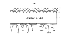
図1は、この発明の実施の形態1による光電変換素子の構成を示す断面図である。図1を参照して、この発明の実施の形態1による光電変換素子100は、n型単結晶シリコン基板1と、酸化膜2と、n型非晶質膜3,21〜2m−1(mは2以上の整数)と、反射防止膜4と、p型非晶質膜11〜1mと、電極31〜3m,41〜4m−1とを備える。
[Embodiment 1]
1 is a cross-sectional view showing a configuration of a photoelectric conversion element according to Embodiment 1 of the present invention. Referring to FIG. 1, a photoelectric conversion element 100 according to Embodiment 1 of the present invention includes an n-type single crystal silicon substrate 1, an oxide film 2, and n-type amorphous films 3, 21 to 2m-1 (m Is an integer of 2 or more), an antireflection film 4, p-type amorphous films 11 to 1m, and electrodes 31 to 3m and 41 to 4m-1.

n型単結晶シリコン基板1は、例えば、(100)の面方位および0.1〜1.0Ω・cmの比抵抗を有する。また、n型単結晶シリコン基板1は、例えば、100〜300μmの厚みを有し、好ましくは、100〜200μmの厚みを有する。そして、n型単結晶シリコン基板1は、光入射側の表面がテクスチャ化されている。   The n-type single crystal silicon substrate 1 has, for example, a (100) plane orientation and a specific resistance of 0.1 to 1.0 Ω · cm. The n-type single crystal silicon substrate 1 has a thickness of 100 to 300 μm, for example, and preferably has a thickness of 100 to 200 μm. The n-type single crystal silicon substrate 1 has a textured surface on the light incident side.

酸化膜2は、二酸化シリコン(SiO)からなり、n型単結晶シリコン基板1の光入射側の表面に接して設けられる。そして、酸化膜2は、例えば、数nmの膜厚を有する。 The oxide film 2 is made of silicon dioxide (SiO 2 ), and is provided in contact with the light incident side surface of the n-type single crystal silicon substrate 1. The oxide film 2 has a film thickness of several nm, for example.

n型非晶質膜3は、非晶質相からなり、例えば、n型a−Siからなる。また、n型非晶質膜3は、例えば、10nm〜数十nmの膜厚を有する。更に、n型非晶質層3のリン(P)濃度は、1×1018cm−3〜1×1020cm−3である。そして、n型非晶質膜3は、酸化膜2に接して形成される。 The n-type amorphous film 3 is made of an amorphous phase, for example, n-type a-Si. The n-type amorphous film 3 has a thickness of 10 nm to several tens of nm, for example. Furthermore, the phosphorus (P) concentration of the n-type amorphous layer 3 is 1 × 10 18 cm −3 to 1 × 10 20 cm −3 . The n-type amorphous film 3 is formed in contact with the oxide film 2.

反射防止膜4は、例えば、シリコンナイトライド(Si)からなり、膜厚は、例えば、100nmである。そして、反射防止膜4は、n型非晶質膜3に接して設けられる。 The antireflection film 4 is made of, for example, silicon nitride (Si 3 N 4 ) and has a film thickness of, for example, 100 nm. The antireflection film 4 is provided in contact with the n-type amorphous film 3.

p型非晶質膜11〜1mの各々は、非晶質相からなり、n型単結晶シリコン基板1の光入射側と反対側の表面に接して設けられる。そして、p型非晶質膜11〜1mの各々は、例えば、p型a−Siからなり、膜厚は、例えば、10nmである。また、p型非晶質膜11〜1mは、n型単結晶シリコン基板1の面内方向において所望の間隔で配置される。更に、p型非晶質膜11〜1mの各々におけるボロン(B)濃度は、例えば、5×1019cm−3である。 Each of p-type amorphous films 11 to 1 m is made of an amorphous phase, and is provided in contact with the surface of n-type single crystal silicon substrate 1 opposite to the light incident side. Each of the p-type amorphous films 11 to 1m is made of, for example, p-type a-Si and has a film thickness of, for example, 10 nm. The p-type amorphous films 11 to 1 m are arranged at a desired interval in the in-plane direction of the n-type single crystal silicon substrate 1. Furthermore, the boron (B) concentration in each of the p-type amorphous films 11 to 1 m is, for example, 5 × 10 19 cm −3 .

n型非晶質膜21〜2m−1の各々は、非晶質相からなる。n型非晶質膜21は、p型非晶質膜11,12およびn型単結晶シリコン基板1に接して配置され、n型非晶質膜22は、p型非晶質膜12,13およびn型単結晶シリコン基板1に接して配置され、以下、同様にして、n型非晶質膜2m−1は、p型非晶質膜1m−1,1mおよびn型単結晶シリコン基板1に接して配置される。   Each of the n-type amorphous films 21 to 2m-1 is made of an amorphous phase. The n-type amorphous film 21 is disposed in contact with the p-type amorphous films 11 and 12 and the n-type single crystal silicon substrate 1, and the n-type amorphous film 22 is formed of the p-type amorphous films 12 and 13. In the same manner, the n-type amorphous film 2m-1 is divided into the p-type amorphous films 1m-1, 1m and the n-type single crystal silicon substrate 1 in the following manner. It is arranged in contact with.

そして、n型非晶質膜21〜2m−1の各々は、例えば、n型a−Siからなり、膜厚は、例えば、10nmである。また、n型非晶質膜21〜2m−1の各々におけるP濃度は、例えば、5×1019cm−3である。 Each of the n-type amorphous films 21 to 2m−1 is made of, for example, n-type a-Si, and has a film thickness of, for example, 10 nm. Further, the P concentration in each of the n-type amorphous films 21 to 2m−1 is, for example, 5 × 10 19 cm −3 .

電極31〜3mは、それぞれ、p型非晶質膜11〜1mに接して設けられる。電極41〜4m−1は、それぞれ、n型非晶質膜21〜2m−1に接して設けられる。そして、電極31〜3m,41〜4m−1の各々は、例えば、銀(Ag)からなる。   The electrodes 31 to 3m are provided in contact with the p-type amorphous films 11 to 1m, respectively. The electrodes 41 to 4m−1 are provided in contact with the n-type amorphous films 21 to 2m−1, respectively. And each of the electrodes 31-3m and 41-4m-1 consists of silver (Ag), for example.

p型非晶質膜11〜1mおよびn型非晶質膜21〜2m−1は、図1の紙面に垂直な方向において同じ長さを有する。そして、p型非晶質膜11〜1mの全体の面積がn型単結晶シリコン基板1の面積に占める割合である面積占有率は、60〜93%であり、n型非晶質膜21〜2m−1の全体の面積がn型単結晶シリコン基板1の面積に占める割合である面積占有率は、5〜20%である。   The p-type amorphous films 11-1m and the n-type amorphous films 21-2m-1 have the same length in the direction perpendicular to the paper surface of FIG. The area occupation ratio, which is the ratio of the entire area of the p-type amorphous film 11 to 1 m to the area of the n-type single crystal silicon substrate 1, is 60 to 93%. The area occupation ratio, which is the ratio of the entire area of 2m−1 to the area of the n-type single crystal silicon substrate 1, is 5 to 20%.

このように、p型非晶質膜11〜1mの面積占有率をn型非晶質膜21〜2m−1の面積占有率よりも大きくするのは、n型単結晶シリコン基板1中で光励起された電子および正孔がpn接合(p型非晶質膜11〜1m/n型単結晶シリコン基板1)によって分離され易くし、光励起された電子および正孔の発電への寄与率を高くするためである。   As described above, the area occupancy of the p-type amorphous films 11 to 1m is made larger than the area occupancy of the n-type amorphous films 21 to 2m-1 by photoexcitation in the n-type single crystal silicon substrate 1. The separated electrons and holes are easily separated by the pn junction (p-type amorphous film 11 to 1 m / n-type single crystal silicon substrate 1), and the contribution ratio of photoexcited electrons and holes to power generation is increased. Because.

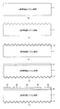
図2〜図4は、それぞれ、図1に示す光電変換素子100の製造方法を示す第1〜第3の工程図である。   2-4 is a 1st-3rd process drawing which respectively shows the manufacturing method of the photoelectric conversion element 100 shown in FIG.

光電変換素子100の製造方法について説明する。光電変換素子100は、プラズマ装置を主に用いてプラズマCVD法によって製造される。   A method for manufacturing the photoelectric conversion element 100 will be described. The photoelectric conversion element 100 is manufactured by a plasma CVD method mainly using a plasma apparatus.

プラズマ装置は、仕込室と、反応室CB1〜CB3と、取出室と、整合器と、RF電源とを備える。仕込室、反応室CB1〜CB3および取出室は、直列に配置されている。そして、仕込室と反応室CB1との間、反応室CB1と反応室CB2との間、反応室CB2と反応室CB3との間、および反応室CB3と取出室との間は、仕切バルブで仕切られている。また、仕込室から反応室CB1、反応室CB2、反応室CB3および取出室へ単結晶シリコン基板を順次搬送する搬送機構がプラズマ装置に備えられている。   The plasma apparatus includes a preparation chamber, reaction chambers CB1 to CB3, an extraction chamber, a matching unit, and an RF power source. The charging chamber, the reaction chambers CB1 to CB3, and the take-out chamber are arranged in series. A partition valve is used to partition between the charging chamber and the reaction chamber CB1, between the reaction chamber CB1 and the reaction chamber CB2, between the reaction chamber CB2 and the reaction chamber CB3, and between the reaction chamber CB3 and the take-out chamber. It has been. Further, the plasma apparatus is provided with a transport mechanism for sequentially transporting the single crystal silicon substrate from the preparation chamber to the reaction chamber CB1, the reaction chamber CB2, the reaction chamber CB3, and the take-out chamber.

仕込室は、加熱機構と排気機構とを備える。加熱機構は、単結晶シリコン基板を所定の温度に昇温する。排気機構は、仕込室内のガスを排気し、仕込室の到達圧力を、例えば、1×10⁻⁵Pa以下に設定する。 The charging chamber includes a heating mechanism and an exhaust mechanism. The heating mechanism raises the temperature of the single crystal silicon substrate to a predetermined temperature. The exhaust mechanism exhausts the gas in the preparation chamber, and sets the ultimate pressure in the preparation chamber to, for example, 1 × 10 −5 Pa or less.

反応室CB1〜CB3の各々は、平行平板電極と、加熱機構と、排気機構とを備える。加熱機構は、単結晶シリコン基板を所定の温度に昇温する。排気機構は、反応室CB1〜CB3内のガスを排気し、反応室CB1〜CB3の到達圧力を、例えば、1×10⁻⁵Pa以下に設定する。平行平板電極は、整合器を介してRF電源に接続される。なお、反応室CB1は、p型a−Siを堆積するための反応室であり、反応室CB2は、n型a−Siを堆積するための反応室であり、反応室CB3は、i型a−Siを堆積するための反応室である。 Each of the reaction chambers CB1 to CB3 includes a parallel plate electrode, a heating mechanism, and an exhaust mechanism. The heating mechanism raises the temperature of the single crystal silicon substrate to a predetermined temperature. The exhaust mechanism exhausts the gases in the reaction chambers CB1 to CB3, and sets the ultimate pressure in the reaction chambers CB1 to CB3 to, for example, 1 × 10 −5 Pa or less. The parallel plate electrodes are connected to an RF power source through a matching unit. The reaction chamber CB1 is a reaction chamber for depositing p-type a-Si, the reaction chamber CB2 is a reaction chamber for depositing n-type a-Si, and the reaction chamber CB3 is an i-type a A reaction chamber for depositing Si.

取出室は、排気機構を備える。排気機構は、取出室内のガスを排気し、取出室の到達圧力を、例えば、1×10⁻⁵Pa以下に設定する。 The take-out chamber includes an exhaust mechanism. The exhaust mechanism exhausts the gas in the extraction chamber and sets the ultimate pressure in the extraction chamber to, for example, 1 × 10 −5 Pa or less.

仕込室、反応室CB1〜CB3および取出室の各排気機構は、ターボ分子ポンプ、メカニカルブースタポンプおよびロータリーポンプからなる。ターボ分子ポンプ、メカニカルブースタポンプおよびロータリーポンプは、ターボ分子ポンプが仕込室、反応室CB1〜CB3および取出室に最も近くなるように、それぞれ、仕込室、反応室CB1〜CB3および取出室に直列的に連結されている。そして、各排気機構は、ターボ分子ポンプ、メカニカルブースタポンプおよびロータリーポンプによって、それぞれ、仕込室、反応室CB1〜CB3および取出室内のガスを排気し、またはメカニカルブースタポンプおよびロータリーポンプによって、それぞれ、仕込室、反応室CB1〜CB3および取出室内のガスを排気する。   Each exhaust mechanism of the charging chamber, the reaction chambers CB1 to CB3, and the take-out chamber includes a turbo molecular pump, a mechanical booster pump, and a rotary pump. The turbo molecular pump, the mechanical booster pump and the rotary pump are serially connected to the charging chamber, the reaction chambers CB1 to CB3 and the extraction chamber, respectively, so that the turbo molecular pump is closest to the charging chamber, the reaction chambers CB1 to CB3 and the extraction chamber. It is connected to. Each exhaust mechanism exhausts the gas in the charging chamber, reaction chambers CB1 to CB3, and the extraction chamber with a turbo molecular pump, a mechanical booster pump, and a rotary pump, respectively, or is charged with a mechanical booster pump and a rotary pump, respectively. The gases in the chamber, reaction chambers CB1 to CB3 and the extraction chamber are exhausted.

RF電源は、例えば、13.56MHzのRF電力を整合器を介して反応室CB1〜CB3の平行平板電極に印加する。   The RF power source applies, for example, RF power of 13.56 MHz to the parallel plate electrodes of the reaction chambers CB1 to CB3 via the matching unit.

光電変換素子100の製造が開始されると、n型単結晶シリコン基板1をエタノール等で超音波洗浄して脱脂し(図2の工程(a)参照)、n型単結晶シリコン基板1の表面をアルカリを用いて化学的に異方性エッチングし、n型単結晶シリコン基板1の表面をテクスチャ化する(図2の工程(b)参照)。   When the manufacture of the photoelectric conversion element 100 is started, the n-type single crystal silicon substrate 1 is ultrasonically cleaned with ethanol or the like and degreased (see step (a) in FIG. 2). Is chemically anisotropically etched using an alkali to texture the surface of the n-type single crystal silicon substrate 1 (see step (b) in FIG. 2).

その後、n型単結晶シリコン基板1をフッ酸中に浸漬してn型単結晶シリコン基板1の表面に形成された自然酸化膜を除去するとともに、n型単結晶シリコン基板1の表面を水素で終端する。   Thereafter, the n-type single crystal silicon substrate 1 is immersed in hydrofluoric acid to remove the natural oxide film formed on the surface of the n-type single crystal silicon substrate 1, and the surface of the n-type single crystal silicon substrate 1 is hydrogenated. Terminate.

n型単結晶シリコン基板1の洗浄が終了すると、n型単結晶シリコン基板1を酸化炉に入れ、1000℃の温度で酸素雰囲気中でn型単結晶シリコン基板1を熱酸化する。この場合、酸化時間は、例えば、数分である。そして、n型単結晶シリコン基板1の片側の表面および端面に形成されたSiOをフッ酸によって除去し、n型単結晶シリコン基板1のテクスチャ化された表面にSiOからなる酸化膜2を形成する(図2の工程(c)参照)。 When the cleaning of the n-type single crystal silicon substrate 1 is completed, the n-type single crystal silicon substrate 1 is put in an oxidation furnace, and the n-type single crystal silicon substrate 1 is thermally oxidized at a temperature of 1000 ° C. in an oxygen atmosphere. In this case, the oxidation time is several minutes, for example. Then, SiO 2 formed on one surface and end face of n-type single crystal silicon substrate 1 is removed by hydrofluoric acid, and oxide film 2 made of SiO 2 is formed on the textured surface of n-type single crystal silicon substrate 1. (See step (c) in FIG. 2).

そして、n型単結晶シリコン基板1/酸化膜2をプラズマ装置の仕込室の基板ホルダー上に配置する。   Then, the n-type single crystal silicon substrate 1 / oxide film 2 is placed on the substrate holder in the preparation chamber of the plasma apparatus.

その後、仕込室の排気機構は、1×10⁻⁵Pa以下に仕込室内のガスを排気し、仕込室の加熱機構は、n型単結晶シリコン基板1/酸化膜2の温度を200℃に設定するように基板ホルダーを加熱する。また、反応室CB1〜CB3の加熱機構も、n型単結晶シリコン基板1/酸化膜2の温度を200℃に設定するように基板ホルダーを加熱する。 After that, the evacuation mechanism in the preparation chamber exhausts the gas in the preparation chamber to 1 × 10 −5 Pa or less, and the heating mechanism in the preparation chamber sets the temperature of the n-type single crystal silicon substrate 1 / oxide film 2 to 200 ° C. Heat the substrate holder so that it does. Further, the heating mechanism of the reaction chambers CB1 to CB3 also heats the substrate holder so that the temperature of the n-type single crystal silicon substrate 1 / oxide film 2 is set to 200.degree.

n型単結晶シリコン基板1/酸化膜2の温度が200℃に達すると、仕込室と反応室CB1との間の仕切バルブが開けられ、n型単結晶シリコン基板1/酸化膜2は、仕込室から反応室CB1へ搬送される。   When the temperature of the n-type single crystal silicon substrate 1 / oxide film 2 reaches 200 ° C., the partition valve between the charging chamber and the reaction chamber CB1 is opened, and the n-type single crystal silicon substrate 1 / oxide film 2 is charged It is conveyed from the chamber to the reaction chamber CB1.

p型非晶質膜11〜1mおよびn型非晶質膜3,21〜2m−1を形成するときの材料ガスの流量を表1に示す。   Table 1 shows the flow rate of the material gas when forming the p-type amorphous films 11 to 1m and the n-type amorphous films 3 and 21 to 2m-1.

Figure 2013125890
Figure 2013125890

n型単結晶シリコン基板1/酸化膜2が反応室CB1へ搬送されると、2sccmのシラン(SiH)ガスと、42sccmの水素(H)ガスと、水素希釈された12sccmのジボラン(B)ガスとを反応室CB1に流し、反応室CB1の圧力を13.3Pa〜665Paの範囲に設定する。そして、RF電源は、16〜80mW/cmの範囲のRFパワーを整合器を介して平行平板電極に印加する。これによって、反応室CB1内でプラズマが発生し、p型a−Siからなるp型非晶質膜20がn型単結晶シリコン基板1の裏面(=酸化膜2が形成された面と反対側の表面)に堆積される(図2の工程(d)参照)。なお、水素希釈されたBガスの濃度は、0.1%である。 When the n-type single crystal silicon substrate 1 / oxide film 2 is transferred to the reaction chamber CB1, 2 sccm of silane (SiH 4 ) gas, 42 sccm of hydrogen (H 2 ) gas, and hydrogen diluted 12 sccm of diborane (B 2 H 6 ) gas is allowed to flow into the reaction chamber CB1, and the pressure in the reaction chamber CB1 is set in the range of 13.3 Pa to 665 Pa. The RF power source applies RF power in the range of 16 to 80 mW / cm 2 to the parallel plate electrodes through the matching unit. As a result, plasma is generated in the reaction chamber CB1, and the p-type amorphous film 20 made of p-type a-Si is formed on the back surface of the n-type single crystal silicon substrate 1 (= the side opposite to the surface on which the oxide film 2 is formed). (See step (d) in FIG. 2). The concentration of B 2 H 6 gas diluted with hydrogen is 0.1%.

p型非晶質膜20の膜厚が10nmになると、反応室CB1の平行平板電極へのRFパワーの印加を停止するとともに、SiHガス、HガスおよびBガスの反応室CB1への供給を停止し、排気機構によって1×10⁻⁵Pa以下に反応室CB1を真空引きする。そして、仕切バルブを開け、p型非晶質膜20/n型単結晶シリコン基板1/酸化膜2を反応室CB1から取出室へ搬送し、p型非晶質膜20/n型単結晶シリコン基板1/酸化膜2を室温まで冷却した後、取り出す。 When the thickness of the p-type amorphous film 20 reaches 10 nm, the application of RF power to the parallel plate electrodes in the reaction chamber CB1 is stopped, and the reaction chamber CB1 of SiH 4 gas, H 2 gas, and B 2 H 6 gas is stopped. And the reaction chamber CB1 is evacuated to 1 × 10 −5 Pa or less by an exhaust mechanism. Then, the gate valve is opened, and the p-type amorphous film 20 / n-type single crystal silicon substrate 1 / oxide film 2 is transferred from the reaction chamber CB1 to the take-out chamber, and the p-type amorphous film 20 / n-type single crystal silicon is transferred. The substrate 1 / oxide film 2 is cooled to room temperature and then taken out.

そして、取り出したp型非晶質膜20/n型単結晶シリコン基板1/酸化膜2のp型非晶質膜20の全面にレジストを塗布し、その塗布したレジストをフォトリソグラフィによってパターンニングしてレジストパターン30を形成する(図2の工程(e)参照)。   Then, a resist is applied to the entire surface of the p-type amorphous film 20 of the extracted p-type amorphous film 20 / n-type single crystal silicon substrate 1 / oxide film 2, and the applied resist is patterned by photolithography. Then, a resist pattern 30 is formed (see step (e) in FIG. 2).

その後、レジストパターン30をマスクとしてp型非晶質膜20をドライエッチングまたはウェットエッチングによってエッチングし、p型非晶質膜11〜1mを形成する(図3の工程(f)参照)。   Thereafter, the p-type amorphous film 20 is etched by dry etching or wet etching using the resist pattern 30 as a mask to form p-type amorphous films 11 to 1m (see step (f) in FIG. 3).

p型非晶質膜11〜1mを形成すると、p型非晶質膜11〜1m/n型単結晶シリコン基板1/酸化膜2のp型非晶質膜11〜1m側をフッ酸で洗浄し、p型非晶質膜11〜1m/n型単結晶シリコン基板1/酸化膜2をプラズマ装置の仕込室の基板ホルダー上に配置する。   When the p-type amorphous films 11 to 1m are formed, the p-type amorphous films 11 to 1m / n-type single crystal silicon substrate 1 / the oxide film 2 on the p-type amorphous films 11 to 1m side are cleaned with hydrofluoric acid. Then, the p-type amorphous films 11 to 1 m / n-type single crystal silicon substrate 1 / oxide film 2 are arranged on the substrate holder in the preparation chamber of the plasma apparatus.

そして、仕込室の排気機構は、1×10⁻⁵Pa以下に仕込室内のガスを排気し、仕込室の加熱機構は、p型非晶質膜11〜1m/n型単結晶シリコン基板1/酸化膜2の温度を200℃に設定するように基板ホルダーを加熱する。 And the exhaust mechanism of the preparation chamber exhausts the gas in the preparation chamber to 1 × 10 −5 Pa or less, and the heating mechanism of the preparation chamber is the p-type amorphous film 11 to 1 m / n type single crystal silicon substrate 1 / The substrate holder is heated so that the temperature of the oxide film 2 is set to 200.degree.

p型非晶質膜11〜1m/n型単結晶シリコン基板1/酸化膜2の温度が200℃に達すると、p型非晶質膜11〜1m/n型単結晶シリコン基板1/酸化膜2を仕込室から反応室CB2へ搬送する。   When the temperature of the p-type amorphous film 11 to 1 m / n type single crystal silicon substrate 1 / oxide film 2 reaches 200 ° C., the p-type amorphous film 11 to 1 m / n type single crystal silicon substrate 1 / oxide film 2 is transferred from the preparation chamber to the reaction chamber CB2.

p型非晶質膜11〜1m/n型単結晶シリコン基板1/酸化膜2が反応室CB2へ搬送されると、20sccmのSiHガスと、150sccmのHガスと、水素希釈された50sccmのフォスフィン(PH)ガスとを反応室CB2に流し(表1参照)、反応室CB2の圧力を13.3Pa〜665Paの範囲に設定する。そして、RF電源は、16〜80mW/cmの範囲のRFパワーを整合器を介して平行平板電極に印加する。これによって、反応室CB2内でプラズマが発生し、n型a−Siからなるn型非晶質膜40がp型非晶質膜11〜1mおよびn型単結晶シリコン基板1の表面に堆積される(図3の工程(g)参照)。なお、水素希釈されたPHガスの濃度は、0.2%である。 When the p-type amorphous film 11 to 1 m / n-type single crystal silicon substrate 1 / oxide film 2 is transferred to the reaction chamber CB2, 20 sccm of SiH 4 gas, 150 sccm of H 2 gas, and 50 sccm diluted with hydrogen are used. Phosphine (PH 3 ) gas is allowed to flow into the reaction chamber CB2 (see Table 1), and the pressure in the reaction chamber CB2 is set in the range of 13.3 Pa to 665 Pa. The RF power source applies RF power in the range of 16 to 80 mW / cm 2 to the parallel plate electrodes through the matching unit. As a result, plasma is generated in the reaction chamber CB2, and an n-type amorphous film 40 made of n-type a-Si is deposited on the surfaces of the p-type amorphous films 11 to 1m and the n-type single crystal silicon substrate 1. (See step (g) in FIG. 3). The concentration of PH 3 gas diluted with hydrogen is 0.2%.

n型非晶質膜40の膜厚が10nmになると、反応室CB2の平行平板電極へのRFパワーの印加を停止するとともに、SiHガス、HガスおよびPHガスの反応室CB2への供給を停止し、排気機構によって1×10⁻⁵Pa以下に反応室CB2を真空引きする。そして、仕切バルブを開け、n型非晶質膜40/p型非晶質膜11〜1m/n型単結晶シリコン基板1/酸化膜2を反応室CB2から取出室へ搬送する。そして、n型非晶質膜40/p型非晶質膜11〜1m/n型単結晶シリコン基板1/酸化膜2を室温まで冷却し、取出室から取出す。 When the thickness of the n-type amorphous film 40 reaches 10 nm, the application of RF power to the parallel plate electrodes in the reaction chamber CB2 is stopped, and SiH 4 gas, H 2 gas, and PH 3 gas are supplied to the reaction chamber CB2. Supply is stopped and the reaction chamber CB2 is evacuated to 1 × 10 −5 Pa or less by an exhaust mechanism. Then, the gate valve is opened, and the n-type amorphous film 40 / p-type amorphous film 11-1m / n-type single crystal silicon substrate 1 / oxide film 2 is transferred from the reaction chamber CB2 to the take-out chamber. Then, the n-type amorphous film 40 / p-type amorphous film 11 to 1m / n-type single crystal silicon substrate 1 / oxide film 2 is cooled to room temperature and taken out from the take-out chamber.

その後、n型非晶質膜40/p型非晶質膜11〜1m/n型単結晶シリコン基板1/酸化膜2のn型非晶質膜40上にレジストを塗布し、その塗布したレジストをフォトリソグラフィによってパターンニングしてレジストパターン50を形成する(図3の工程(h)参照)。   Thereafter, a resist is applied on the n-type amorphous film 40 / p-type amorphous film 11-1m / n-type single crystal silicon substrate 1 / n-type amorphous film 40 of the oxide film 2, and the applied resist Is patterned by photolithography to form a resist pattern 50 (see step (h) in FIG. 3).

その後、レジストパターン50をマスクとしてn型非晶質膜40をドライエッチングまたはウェットエッチングによってエッチングし、n型非晶質膜21〜2m−1を形成する(図3の工程(i)参照)。   Thereafter, the n-type amorphous film 40 is etched by dry etching or wet etching using the resist pattern 50 as a mask to form n-type amorphous films 21 to 2m−1 (see step (i) in FIG. 3).

そして、n型非晶質膜21〜2m−1/p型非晶質膜11〜1m/n型単結晶シリコン基板1/酸化膜2をフッ酸で洗浄し、n型非晶質膜21〜2m−1/p型非晶質膜11〜1m/n型単結晶シリコン基板1/酸化膜2をプラズマ装置の仕込室の基板ホルダー上に配置する。なお、酸化膜2は、フッ酸によってエッチングされるが、フッ酸の濃度を薄くすることによって酸化膜2をエッチングすることなしに酸化膜2を洗浄できる。   Then, the n-type amorphous films 21-2m-1 / p-type amorphous films 11-1m / n-type single crystal silicon substrate 1 / oxide film 2 are washed with hydrofluoric acid, The 2m-1 / p-type amorphous film 11 to 1m / n-type single crystal silicon substrate 1 / oxide film 2 are arranged on the substrate holder in the preparation chamber of the plasma apparatus. Although the oxide film 2 is etched by hydrofluoric acid, the oxide film 2 can be cleaned without etching the oxide film 2 by reducing the concentration of hydrofluoric acid.

その後、仕込室の排気機構は、1×10⁻⁵Pa以下に仕込室内のガスを排気し、仕込室の加熱機構は、n型非晶質膜21〜2m−1/p型非晶質膜11〜1m/n型単結晶シリコン基板1/酸化膜2の温度を200℃に設定するように基板ホルダーを加熱する。 Then, the exhaust mechanism of the preparation chamber exhausts the gas in the preparation chamber to 1 × 10 −5 Pa or less, and the heating mechanism of the preparation chamber is the n-type amorphous film 21-2m−1 / p-type amorphous film. The substrate holder is heated so that the temperature of the 11-1 m / n type single crystal silicon substrate 1 / oxide film 2 is set to 200.degree.

n型非晶質膜21〜2m−1/p型非晶質膜11〜1m/n型単結晶シリコン基板1/酸化膜2の温度が200℃に達すると、n型非晶質膜21〜2m−1/p型非晶質膜11〜1m/n型単結晶シリコン基板1/酸化膜2を仕込室から反応室CB2へ搬送する。   When the temperature of n-type amorphous film 21-2m-1 / p-type amorphous film 11-1m / n-type single crystal silicon substrate 1 / oxide film 2 reaches 200 ° C., n-type amorphous film 21-1-2 2m-1 / p type amorphous film 11-1m / n type single crystal silicon substrate 1 / oxide film 2 is transferred from the preparation chamber to reaction chamber CB2.

n型非晶質膜21〜2m−1/p型非晶質膜11〜1m/n型単結晶シリコン基板1/酸化膜2が反応室CB2へ搬送されると、20sccmのSiHガスと、150sccmのHガスと、水素希釈された50sccmのPHガスとを反応室CB2に流し(表1参照)、反応室CB2の圧力を13.3Pa〜665Paの範囲に設定する。そして、RF電源は、16〜80mW/cmの範囲のRFパワーを整合器を介して平行平板電極に印加する。これによって、反応室CB2内でプラズマが発生し、n型a−Siからなるn型非晶質膜3が酸化膜2上に堆積される(図4の工程(j)参照)。 When n-type amorphous film 21-2m-1 / p-type amorphous film 11-1m / n-type single crystal silicon substrate 1 / oxide film 2 is transferred to reaction chamber CB2, 20 sccm of SiH 4 gas, A 150 sccm H 2 gas and a hydrogen-diluted 50 sccm PH 3 gas are allowed to flow into the reaction chamber CB 2 (see Table 1), and the pressure in the reaction chamber CB 2 is set to a range of 13.3 Pa to 665 Pa. The RF power source applies RF power in the range of 16 to 80 mW / cm 2 to the parallel plate electrodes through the matching unit. As a result, plasma is generated in the reaction chamber CB2, and an n-type amorphous film 3 made of n-type a-Si is deposited on the oxide film 2 (see step (j) in FIG. 4).

n型非晶質膜3の膜厚が10nm〜数十nmになると、反応室CB2の平行平板電極へのRFパワーの印加を停止するとともに、SiHガス、HガスおよびPHガスの反応室CB2への供給を停止し、排気機構によって1×10⁻⁵Pa以下に反応室CB2を真空引きする。そして、仕切バルブを開け、n型非晶質膜21〜2m−1/p型非晶質膜11〜1m/n型単結晶シリコン基板1/酸化膜2/n型非晶質膜3を反応室CB2から取出室へ搬送する。そして、n型非晶質膜21〜2m−1/p型非晶質膜11〜1m/n型単結晶シリコン基板1/酸化膜2/n型非晶質膜3を室温まで冷却し、取出室から取出す。 When the thickness of the n-type amorphous film 3 becomes 10 nm to several tens of nm, the application of RF power to the parallel plate electrode of the reaction chamber CB2 is stopped and the reaction of SiH 4 gas, H 2 gas and PH 3 gas is stopped. The supply to the chamber CB2 is stopped, and the reaction chamber CB2 is evacuated to 1 × 10 −5 Pa or less by an exhaust mechanism. Then, the gate valve is opened, and the n-type amorphous film 21-2m-1 / p-type amorphous film 11-1m / n-type single crystal silicon substrate 1 / oxide film 2 / n-type amorphous film 3 reacts. It is transferred from the room CB2 to the take-out room. Then, the n-type amorphous film 21-2m-1 / p-type amorphous film 11-1m / n-type single crystal silicon substrate 1 / oxide film 2 / n-type amorphous film 3 is cooled to room temperature and taken out. Remove from room.

その後、n型非晶質膜21〜2m−1/p型非晶質膜11〜1m/n型単結晶シリコン基板1/酸化膜2/n型非晶質膜3のn型非晶質膜3上にSiからなる反射防止膜4をスパッタリングによって形成する(図4の工程(k)参照)。 Thereafter, n-type amorphous film 21-2m-1 / p-type amorphous film 11-1m / n-type single crystal silicon substrate 1 / oxide film 2 / n-type amorphous film 3 n-type amorphous film An antireflection film 4 made of Si 3 N 4 is formed on the substrate 3 by sputtering (see step (k) in FIG. 4).

引き続いて、n型非晶質膜21〜2m−1およびp型非晶質膜11〜1m側にAgを蒸着し、その蒸着したAgをフォトリソグラフィおよびエッチングによってパターンニングし、電極31〜3m,41〜4m−1を形成する。これによって、光電変換素子100が完成する(図4の工程(l)参照)。   Subsequently, Ag is vapor-deposited on the n-type amorphous films 21 to 2m-1 and the p-type amorphous films 11 to 1m side, and the deposited Ag is patterned by photolithography and etching to form electrodes 31 to 3m, 41-4m-1. Thus, the photoelectric conversion element 100 is completed (see step (l) in FIG. 4).

光電変換素子100の製造方法においては、図2の工程(c)において、化学堆積法(CVD:Chemical Vapour Deposition)によって酸化膜2を形成してもよく、酸化液を用いた酸化によって酸化膜2を形成してもよく、室温で水中に浸漬する、または沸騰水中に浸漬する水中酸化法によって酸化膜2を形成してもよく、自然酸化法によって酸化膜2を形成してもよい。自然酸化法によって酸化膜2を形成する場合、即ち、酸化膜2が自然酸化膜からなる場合、n型単結晶シリコン基板1の一方の表面をテクスチャ化した後、そのテクスチャ化した表面を除いてn型単結晶シリコン基板1をフッ酸で洗浄し、その後、工程(d)〜工程(l)を順次実行する。   In the manufacturing method of the photoelectric conversion element 100, the oxide film 2 may be formed by a chemical vapor deposition (CVD) method in the step (c) of FIG. 2, and the oxide film 2 may be formed by oxidation using an oxidizing solution. The oxide film 2 may be formed by an underwater oxidation method that is immersed in water at room temperature or immersed in boiling water, or the oxide film 2 may be formed by a natural oxidation method. When the oxide film 2 is formed by a natural oxidation method, that is, when the oxide film 2 is made of a natural oxide film, after texturing one surface of the n-type single crystal silicon substrate 1, the textured surface is removed. The n-type single crystal silicon substrate 1 is washed with hydrofluoric acid, and then the steps (d) to (l) are sequentially performed.

また、光電変換素子100の製造方法においては、酸化膜2を形成した後、n型非晶質膜3,21〜2m−1、p型非晶質膜11〜1m、反射防止膜4および電極31〜3m,41〜4m−1を形成する順序は、上述した工程(a)〜工程(l)において説明した順序に限らず、任意の順序であってもよい。   Moreover, in the manufacturing method of the photoelectric conversion element 100, after forming the oxide film 2, the n-type amorphous films 3, 21 to 2m-1, the p-type amorphous films 11 to 1m, the antireflection film 4 and the electrodes The order of forming 31 to 3m and 41 to 4m-1 is not limited to the order described in the above-described step (a) to step (l), and may be any order.

光電変換素子100において、太陽光が反射防止膜4側から光電変換素子100に照射されると、n型単結晶シリコン基板1中で電子および正孔が光励起される。   In the photoelectric conversion element 100, when sunlight is irradiated to the photoelectric conversion element 100 from the antireflection film 4 side, electrons and holes are photoexcited in the n-type single crystal silicon substrate 1.

光励起された電子および正孔は、酸化膜2側へ拡散しても、酸化膜2によるn型単結晶シリコン基板1のパッシベーション効果およびn型非晶質膜3によるFSF効果(表面電界効果)によって再結合し難くなり、p型非晶質膜11〜1mおよびn型非晶質膜21〜2m−1側へ拡散し易くなる。   Even though the photoexcited electrons and holes diffuse to the oxide film 2 side, the passivation effect of the n-type single crystal silicon substrate 1 by the oxide film 2 and the FSF effect (surface electric field effect) by the n-type amorphous film 3 It becomes difficult to recombine, and it becomes easy to diffuse to the p-type amorphous films 11-1m and the n-type amorphous films 21-2m-1 side.

より具体的には、n型単結晶シリコン基板1のテクスチャ化された表面に酸化膜2(=SiO)が接しているので、n型単結晶シリコン基板1と酸化膜2(=SiO)との界面における界面準位密度は、1010cm−2〜1011cm−2と非常に低い。その結果、キャリア(電子および正孔)は、n型単結晶シリコン基板1のテクスチャ化された表面において殆ど再結合しない。また、酸化膜2の膜厚は、上述したように数nmであるので、キャリア(電子および正孔)は、n型非晶質膜3によるFSF効果によってn型単結晶シリコン基板1と酸化膜2との界面へ到達し難くなり、再結合が更に抑制される。特に、少数キャリアである正孔の再結合が抑制される。即ち、n型非晶質膜3を構成するn型a−Siの光学バンドギャップ(=約1.7eV)および活性化エネルギー(=約0.2eV〜0.3eV)とn型単結晶シリコン基板1の光学バンドギャップ(=1.1eV)および活性化エネルギー(=0.1eV〜0.2eV)とを考慮すると、n型a−Siの価電子帯の端は、n型単結晶シリコン基板1の価電子帯の端よりも、0.4eV〜0.6eVだけ高エネルギー側に存在するので、n型非晶質膜3は、n型単結晶シリコン基板1の表面近傍において表面電界を発生する。その結果、n型単結晶シリコン基板1の表面近傍へ拡散した正孔は、n型非晶質膜3による表面電界によってn型単結晶シリコン基板1と酸化膜2との界面へ到達し難くなる。従って、少数キャリアである正孔の再結合がFSF効果によって抑制される。 More specifically, since the oxide film 2 (= SiO 2 ) is in contact with the textured surface of the n-type single crystal silicon substrate 1, the n-type single crystal silicon substrate 1 and the oxide film 2 (= SiO 2 ) The interface state density at the interface is very low, 10 10 cm −2 to 10 11 cm −2 . As a result, carriers (electrons and holes) hardly recombine on the textured surface of the n-type single crystal silicon substrate 1. Since the thickness of the oxide film 2 is several nm as described above, carriers (electrons and holes) are separated from the n-type single crystal silicon substrate 1 and the oxide film by the FSF effect of the n-type amorphous film 3. It becomes difficult to reach the interface with 2, and recombination is further suppressed. In particular, recombination of holes that are minority carriers is suppressed. That is, the optical band gap (= about 1.7 eV) and activation energy (= about 0.2 eV to 0.3 eV) of n-type a-Si constituting the n-type amorphous film 3 and the n-type single crystal silicon substrate When the optical band gap (= 1.1 eV) and activation energy (= 0.1 eV to 0.2 eV) of 1 are considered, the end of the valence band of n-type a-Si is the n-type single crystal silicon substrate 1 The n-type amorphous film 3 generates a surface electric field in the vicinity of the surface of the n-type single crystal silicon substrate 1 because it exists on the higher energy side by 0.4 eV to 0.6 eV than the end of the valence band. . As a result, the holes diffused near the surface of the n-type single crystal silicon substrate 1 are difficult to reach the interface between the n-type single crystal silicon substrate 1 and the oxide film 2 due to the surface electric field generated by the n-type amorphous film 3. . Accordingly, recombination of holes that are minority carriers is suppressed by the FSF effect.

このように、キャリア(電子および正孔)は、酸化膜2およびn型非晶質膜3によってn型単結晶シリコン基板1の表面における再結合が抑制され、p型非晶質膜11〜1mおよびn型非晶質膜21〜2m−1側へ拡散し易くなる。   Thus, carriers (electrons and holes) are suppressed from recombination on the surface of the n-type single crystal silicon substrate 1 by the oxide film 2 and the n-type amorphous film 3, and the p-type amorphous films 11 to 1 m. And it becomes easy to diffuse to the n-type amorphous films 21-2m-1.

そして、p型非晶質膜11〜1mおよびn型非晶質膜21〜2m−1側へ拡散した電子および正孔は、p型非晶質膜11〜1m/n型単結晶シリコン基板1(=pn接合)による内部電界によって分離され、正孔は、p型非晶質膜11〜1mを介して電極31〜3mへ到達し、電子は、n型非晶質膜21〜2m−1を介して電極41〜4m−1へ到達する。   Then, the electrons and holes diffused toward the p-type amorphous films 11 to 1m and the n-type amorphous films 21 to 2m-1 are transferred to the p-type amorphous films 11 to 1m / n-type single crystal silicon substrate 1. (= Pn junction) is separated by an internal electric field, holes reach the electrodes 31 to 3 m via the p-type amorphous films 11 to 1 m, and electrons are n-type amorphous films 21 to 2 m−1. To reach the electrodes 41-4m-1.

電極41〜4m−1へ到達した電子は、電極31〜3mと電極41〜4m−1との間に接続された負荷を介して電極31〜3mへ到達し、正孔と再結合する。   The electrons that have reached the electrodes 41 to 4m-1 reach the electrodes 31 to 3m via a load connected between the electrodes 31 to 3m and the electrodes 41 to 4m-1, and recombine with the holes.

このように、光電変換素子100は、n型単結晶シリコン基板1中で光励起された電子および正孔をn型単結晶シリコン基板1の裏面(=酸化膜2が形成されたn型単結晶シリコン基板1の表面と反対側の面)から取り出すバックコンタクト型の光電変換素子である。   In this manner, the photoelectric conversion element 100 converts the electrons and holes photoexcited in the n-type single crystal silicon substrate 1 into the back surface of the n-type single crystal silicon substrate 1 (= n-type single crystal silicon on which the oxide film 2 is formed). This is a back contact type photoelectric conversion element taken out from the surface opposite to the surface of the substrate 1.

そして、光電変換素子100は、光入射側に、酸化膜2およびn型非晶質膜3を備えるので、上述したように、n型単結晶シリコン基板1の光入射側の表面においてキャリアの再結合が抑制され、n型単結晶シリコン基板1に対するパッシベーション効果を向上できる。   Further, since the photoelectric conversion element 100 includes the oxide film 2 and the n-type amorphous film 3 on the light incident side, as described above, the carrier is regenerated on the surface of the n-type single crystal silicon substrate 1 on the light incident side. Coupling is suppressed and the passivation effect on the n-type single crystal silicon substrate 1 can be improved.

また、光電変換素子100の製造方法において説明したように、酸化膜2を形成した後に、p型非晶質膜11〜1m、n型非晶質膜3,21〜2m−1、反射防止膜4および電極31〜3m,41〜4m−1を形成するので(図2の工程(d)〜図4の工程(k)参照)、光電変換素子100の製造プロセスにおいて、n型単結晶シリコン基板1の受光面側の表面を保護できる。   In addition, as described in the method for manufacturing the photoelectric conversion element 100, after forming the oxide film 2, the p-type amorphous films 11 to 1m, the n-type amorphous films 3, 21 to 2m-1, and the antireflection film 4 and electrodes 31 to 3m, 41 to 4m-1 (see step (d) in FIG. 2 to step (k) in FIG. 4), in the manufacturing process of the photoelectric conversion element 100, an n-type single crystal silicon substrate The surface on the light receiving surface side of 1 can be protected.

図5は、実施の形態1による他の光電変換素子の構成を示す断面図である。実施の形態1による光電変換素子は、図5に示す光電変換素子100Aであってもよい。   FIG. 5 is a cross-sectional view showing the configuration of another photoelectric conversion element according to the first embodiment. The photoelectric conversion element according to Embodiment 1 may be a photoelectric conversion element 100A illustrated in FIG.

図5を参照して、光電変換素子100Aは、図1に示す光電変換素子100にi型非晶質膜51〜5mを追加したものであり、その他は、光電変換素子100と同じである。   Referring to FIG. 5, the photoelectric conversion element 100 </ b> A is obtained by adding i-type amorphous films 51 to 5 m to the photoelectric conversion element 100 illustrated in FIG. 1, and is otherwise the same as the photoelectric conversion element 100.

i型非晶質膜51〜5mは、非晶質相からなり、それぞれ、n型単結晶シリコン基板1およびp型非晶質膜11〜1mに接し、n型単結晶シリコン基板1とp型非晶質膜11〜1mとの間に配置される。そして、i型非晶質膜51〜5mの各々は、例えば、i型a−Siからなり、膜厚は、例えば、10nmである。また、i型非晶質膜51〜5mは、n型単結晶シリコン基板1の面内方向(図5の紙面における左右方向)において、それぞれ、p型非晶質膜11〜1mと同じ幅を有する。更に、i型非晶質膜51〜5mは、図5の紙面に垂直な方向において、それぞれ、p型非晶質膜11〜1mと同じ長さを有する。   The i-type amorphous films 51 to 5m are made of an amorphous phase and are in contact with the n-type single crystal silicon substrate 1 and the p-type amorphous films 11 to 1m, respectively. It arrange | positions between the amorphous | non-crystalline films 11-1m. Each of the i-type amorphous films 51 to 5m is made of, for example, i-type a-Si, and has a film thickness of, for example, 10 nm. In addition, the i-type amorphous films 51 to 5m have the same width as the p-type amorphous films 11 to 1m in the in-plane direction of the n-type single crystal silicon substrate 1 (the left-right direction in the drawing of FIG. 5), respectively. Have. Further, the i-type amorphous films 51 to 5m have the same length as the p-type amorphous films 11 to 1m, respectively, in the direction perpendicular to the paper surface of FIG.

光電変換素子100Aにおいては、n型非晶質膜21〜2m−1の各々の膜厚は、p型非晶質膜11〜1mの膜厚とi型非晶質膜61〜6mの膜厚との合計膜厚からなる。   In the photoelectric conversion element 100A, the thicknesses of the n-type amorphous films 21 to 2m−1 are the thicknesses of the p-type amorphous films 11 to 1m and the i-type amorphous films 61 to 6m. And the total film thickness.

また、光電変換素子100Aにおいては、i型非晶質膜51の端面は、n型非晶質膜21に接し、i型非晶質膜52の端面は、n型非晶質膜21,22に接し、i型非晶質膜53の端面は、n型非晶質膜22,23に接し、以下、同様にして、i型非晶質膜5m−1の端面は、n型非晶質膜2m−2,2m−1に接し、i型非晶質膜5mの端面は、n型非晶質膜2m−1に接する。   In the photoelectric conversion element 100A, the end surface of the i-type amorphous film 51 is in contact with the n-type amorphous film 21, and the end surface of the i-type amorphous film 52 is the n-type amorphous film 21, 22. The end surface of the i-type amorphous film 53 is in contact with the n-type amorphous films 22 and 23. Similarly, the end surface of the i-type amorphous film 5m-1 is the n-type amorphous film. The end surfaces of the i-type amorphous film 5m are in contact with the n-type amorphous film 2m-1 in contact with the films 2m-2 and 2m-1.

光電変換素子100Aは、図2〜図4に示す工程(a)〜工程(l)によって製造される。この場合、図2の工程(d)において、i型非晶質膜51〜5m用のi型非晶質膜がプラズマCVD法によってn型単結晶シリコン基板1上に堆積され、その後、p型非晶質膜11〜1m用のp型非晶質膜20がプラズマCVD法によってi型非晶質膜51〜5m用のi型非晶質膜上に堆積される。そして、i型非晶質膜51〜5m用のi型非晶質膜を堆積するときのガス流量は、表1に示すとおりである。また、i型非晶質膜51〜5m用のi型非晶質膜を堆積するときの圧力およびRFパワーは、p型非晶質膜11〜1mおよびn型非晶質膜21〜2m−1を形成するときの圧力およびRFパワーと同じである。   100 A of photoelectric conversion elements are manufactured by the process (a)-process (l) shown in FIGS. In this case, in step (d) of FIG. 2, an i-type amorphous film for the i-type amorphous films 51 to 5m is deposited on the n-type single crystal silicon substrate 1 by the plasma CVD method, and then the p-type is formed. A p-type amorphous film 20 for the amorphous films 11 to 1m is deposited on the i-type amorphous film for the i-type amorphous films 51 to 5m by plasma CVD. The gas flow rate when depositing the i-type amorphous films for the i-type amorphous films 51 to 5 m is as shown in Table 1. The pressure and RF power when depositing the i-type amorphous film for the i-type amorphous film 51-5m are p-type amorphous film 11-1m and n-type amorphous film 21-2m- The pressure and RF power when forming 1 are the same.

光電変換素子100Aにおける発電機構は、光電変換素子100の発電機構と概ね同じであり、光電変換素子100において説明したように、電子および正孔は、n型単結晶シリコン基板1の光入射側の表面(テクスチャ化された表面)における再結合が抑制され、p型非晶質膜11〜1mおよびn型非晶質膜21〜2m−1側へ拡散し易くなる。そして、p型非晶質膜11〜1mおよびn型非晶質膜21〜2m−1側へ拡散した電子および正孔は、p型非晶質膜11〜1m/i型非晶質膜51〜5m/n型単結晶シリコン基板1(=pin接合)による内部電界によって分離され、正孔は、i型非晶質膜51〜5mおよびp型非晶質膜11〜1mを介して電極31〜3mへ到達し、電子は、n型非晶質膜21〜2m−1を介して電極41〜4m−1へ到達する。   The power generation mechanism in the photoelectric conversion element 100A is substantially the same as the power generation mechanism in the photoelectric conversion element 100. As described in the photoelectric conversion element 100, electrons and holes are on the light incident side of the n-type single crystal silicon substrate 1. Recombination on the surface (textured surface) is suppressed, and diffusion to the p-type amorphous films 11-1m and n-type amorphous films 21-2m-1 side is facilitated. Then, the electrons and holes diffused toward the p-type amorphous film 11 to 1 m and the n-type amorphous film 21 to 2 m−1 side are converted into the p-type amorphous film 11 to 1 m / i-type amorphous film 51. ~ 5 m / n type single crystal silicon substrate 1 (= pin junction) is separated by an internal electric field, and holes are separated by electrodes 31 via i-type amorphous films 51 to 5 m and p-type amorphous films 11 to 1 m. To 3m, and the electrons reach the electrodes 41 to 4m-1 through the n-type amorphous films 21 to 2m-1.

電極41〜4m−1へ到達した電子は、電極31〜3mと電極41〜4m−1との間に接続された負荷を介して電極31〜3mへ到達し、正孔と再結合する。   The electrons that have reached the electrodes 41 to 4m-1 reach the electrodes 31 to 3m via a load connected between the electrodes 31 to 3m and the electrodes 41 to 4m-1, and recombine with the holes.

このように、光電変換素子100Aは、n型単結晶シリコン基板1中で光励起された電子および正孔をn型単結晶シリコン基板1の裏面(=酸化膜2が形成されたn型単結晶シリコン基板1の表面と反対側の面)から取り出すバックコンタクト型の光電変換素子である。   As described above, the photoelectric conversion element 100 </ b> A converts the electrons and holes photoexcited in the n-type single crystal silicon substrate 1 into the back surface of the n-type single crystal silicon substrate 1 (= n-type single crystal silicon on which the oxide film 2 is formed). This is a back contact type photoelectric conversion element taken out from the surface opposite to the surface of the substrate 1.

そして、光電変換素子100Aは、n型単結晶シリコン基板1の光入射側の表面(テクスチャ化された表面)に接して設けられた酸化膜2と、酸化膜2に接して設けられたn型非晶質膜3とを備えるので、光電変換素子100において説明したように、n型単結晶シリコン基板1に対するパッシベーション効果を向上できる。   The photoelectric conversion element 100A includes an oxide film 2 provided in contact with the light incident surface (textured surface) of the n-type single crystal silicon substrate 1, and an n-type provided in contact with the oxide film 2. Since the amorphous film 3 is provided, the passivation effect on the n-type single crystal silicon substrate 1 can be improved as described in the photoelectric conversion element 100.

また、光電変換素子100Aにおいては、n型単結晶シリコン基板1とp型非晶質膜11〜1mとの間にi型非晶質膜51〜5mが存在するので、n型単結晶シリコン基板1とp型非晶質膜11〜1mとの界面における正孔の再結合が抑制される。その結果、短絡光電流が増加し、光電変換素子100Aの変換効率を向上できる。   In the photoelectric conversion element 100A, since the i-type amorphous films 51 to 5m exist between the n-type single crystal silicon substrate 1 and the p-type amorphous films 11 to 1m, the n-type single crystal silicon substrate Recombination of holes at the interface between 1 and the p-type amorphous films 11 to 1 m is suppressed. As a result, the short-circuit photocurrent increases and the conversion efficiency of the photoelectric conversion element 100A can be improved.

光電変換素子100Aについてのその他の説明は、光電変換素子100についての説明と同じである。   The other description of the photoelectric conversion element 100A is the same as the description of the photoelectric conversion element 100.

図6は、実施の形態1による更に他の光電変換素子の構成を示す断面図である。実施の形態1による光電変換素子は、図6に示す光電変換素子100Bであってもよい。   FIG. 6 is a cross-sectional view showing a configuration of still another photoelectric conversion element according to Embodiment 1. The photoelectric conversion element according to Embodiment 1 may be a photoelectric conversion element 100B illustrated in FIG.

図6を参照して、光電変換素子100Bは、図1に示す光電変換素子100にi型非晶質膜61〜6m−1を追加したものであり、その他は、光電変換素子100と同じである。   Referring to FIG. 6, photoelectric conversion element 100B is obtained by adding i-type amorphous films 61 to 6m-1 to photoelectric conversion element 100 shown in FIG. is there.

i型非晶質膜61〜6m−1は、非晶質相からなり、それぞれ、n型単結晶シリコン基板1およびn型非晶質膜21〜2m−1に接し、n型単結晶シリコン基板1とn型非晶質膜21〜2m−1との間に配置される。そして、i型非晶質膜61〜6m−1の各々は、例えば、i型a−Siからなり、膜厚は、例えば、10nmである。また、i型非晶質膜61〜6m−1は、図6の紙面に垂直な方向において、それぞれ、n型非晶質膜21〜2m−1と同じ長さを有する。   The i-type amorphous films 61 to 6m-1 are made of an amorphous phase and are in contact with the n-type single crystal silicon substrate 1 and the n-type amorphous films 21 to 2m-1, respectively. 1 and n-type amorphous films 21-2m-1. Each of the i-type amorphous films 61 to 6m-1 is made of, for example, i-type a-Si and has a film thickness of, for example, 10 nm. The i-type amorphous films 61 to 6m-1 have the same length as the n-type amorphous films 21 to 2m-1 in the direction perpendicular to the paper surface of FIG.

光電変換素子100Bにおいては、p型非晶質膜11〜1mの各々の膜厚は、n型非晶質膜21〜2m−1の膜厚とi型非晶質膜61〜6m−1の膜厚との合計膜厚からなる。   In the photoelectric conversion element 100B, each of the p-type amorphous films 11 to 1m has a thickness of the n-type amorphous films 21 to 2m-1 and that of the i-type amorphous films 61 to 6m-1. It consists of the total film thickness with the film thickness.

また、光電変換素子100Bにおいては、p型非晶質膜11の端面は、i型非晶質膜61およびn型非晶質膜21に接し、p型非晶質膜12の端面は、i型非晶質膜61およびn型非晶質膜21とi型非晶質膜62およびn型非晶質膜22とに接し、p型非晶質膜13の端面は、i型非晶質膜62およびn型非晶質膜22とi型非晶質膜63およびn型非晶質膜23とに接し、以下、同様にして、p型非晶質膜1m−1の端面は、i型非晶質膜6m−2およびn型非晶質膜2m−2とi型非晶質膜6m−1およびn型非晶質膜2m−1とに接し、p型非晶質膜1mの端面は、i型非晶質膜6m−1およびn型非晶質膜2m−1に接する。   In the photoelectric conversion element 100B, the end surface of the p-type amorphous film 11 is in contact with the i-type amorphous film 61 and the n-type amorphous film 21, and the end surface of the p-type amorphous film 12 is i. The end surface of the p-type amorphous film 13 is in contact with the i-type amorphous film 61 and the n-type amorphous film 21 and the i-type amorphous film 62 and the n-type amorphous film 22. The end face of the p-type amorphous film 1m-1 is in contact with the film 62 and the n-type amorphous film 22 and the i-type amorphous film 63 and the n-type amorphous film 23. Of the p-type amorphous film 1m in contact with the n-type amorphous film 6m-2 and the n-type amorphous film 2m-2 and the i-type amorphous film 6m-1 and the n-type amorphous film 2m-1. The end face is in contact with the i-type amorphous film 6m-1 and the n-type amorphous film 2m-1.

光電変換素子100Bは、図2〜図4に示す工程(a)〜工程(l)によって製造される。この場合、図3の工程(i)において、i型非晶質膜61〜6m−1用のi型非晶質膜がプラズマCVD法によってn型単結晶シリコン基板1およびp型非晶質膜11〜1m上に堆積され、その後、n型非晶質膜60がプラズマCVD法によってi型非晶質膜61〜6m−1用のi型非晶質膜上に堆積される。そして、i型非晶質膜61〜6m−1用のi型非晶質膜を堆積するときのガス流量は、表1に示すi型非晶質膜51〜5mのガス流量と同じである。   The photoelectric conversion element 100B is manufactured by steps (a) to (l) shown in FIGS. In this case, in step (i) of FIG. 3, the i-type amorphous film for the i-type amorphous films 61 to 6m-1 is converted into the n-type single crystal silicon substrate 1 and the p-type amorphous film by the plasma CVD method. Then, the n-type amorphous film 60 is deposited on the i-type amorphous film for the i-type amorphous films 61 to 6m-1 by the plasma CVD method. The gas flow rate when depositing the i-type amorphous film for the i-type amorphous film 61-6m-1 is the same as the gas flow rate of the i-type amorphous film 51-5m shown in Table 1. .

光電変換素子100Bにおける発電機構は、光電変換素子100の発電機構と概ね同じであり、光電変換素子100において説明したように、電子および正孔は、n型単結晶シリコン基板1の光入射側の表面(テクスチャ化された表面)における再結合が抑制され、p型非晶質膜11〜1mおよびn型非晶質膜21〜2m−1側へ拡散し易くなる。そして、p型非晶質膜11〜1mおよびn型非晶質膜21〜2m−1側へ拡散した電子および正孔は、p型非晶質膜11〜1m/n型単結晶シリコン基板1(=pn接合)による内部電界によって分離され、正孔は、p型非晶質膜11〜1mを介して電極31〜3mへ到達し、電子は、i型非晶質膜61〜6m−1およびn型非晶質膜21〜2m−1を介して電極41〜4m−1へ到達する。   The power generation mechanism in the photoelectric conversion element 100B is substantially the same as the power generation mechanism in the photoelectric conversion element 100. As described in the photoelectric conversion element 100, electrons and holes are on the light incident side of the n-type single crystal silicon substrate 1. Recombination on the surface (textured surface) is suppressed, and diffusion to the p-type amorphous films 11-1m and n-type amorphous films 21-2m-1 side is facilitated. Then, the electrons and holes diffused toward the p-type amorphous films 11 to 1m and the n-type amorphous films 21 to 2m-1 are transferred to the p-type amorphous films 11 to 1m / n-type single crystal silicon substrate 1. (= Pn junction) is separated by an internal electric field, holes reach the electrodes 31 to 3m via the p-type amorphous films 11 to 1m, and the electrons are i-type amorphous films 61 to 6m-1 And it reaches the electrodes 41-4m-1 through the n-type amorphous films 21-2m-1.

電極41〜4m−1へ到達した電子は、電極31〜3mと電極41〜4m−1との間に接続された負荷を介して電極31〜3mへ到達し、正孔と再結合する。   The electrons that have reached the electrodes 41 to 4m-1 reach the electrodes 31 to 3m via a load connected between the electrodes 31 to 3m and the electrodes 41 to 4m-1, and recombine with the holes.

このように、光電変換素子100Bは、n型単結晶シリコン基板1中で光励起された電子および正孔をn型単結晶シリコン基板1の裏面(=酸化膜2が形成されたn型単結晶シリコン基板1の表面と反対側の面)から取り出すバックコンタクト型の光電変換素子である。   As described above, the photoelectric conversion element 100 </ b> B uses electrons and holes photoexcited in the n-type single crystal silicon substrate 1 to convert the back surface of the n-type single crystal silicon substrate 1 (= n-type single crystal silicon on which the oxide film 2 is formed). This is a back contact type photoelectric conversion element taken out from the surface opposite to the surface of the substrate 1.

そして、光電変換素子100Bは、n型単結晶シリコン基板1の光入射側の表面(テクスチャ化された表面)に接して設けられた酸化膜2と、酸化膜2に接して設けられたn型非晶質膜3とを備えるので、光電変換素子100において説明したように、n型単結晶シリコン基板1に対するパッシベーション効果を向上できる。   The photoelectric conversion element 100B includes an oxide film 2 provided in contact with the light incident side surface (textured surface) of the n-type single crystal silicon substrate 1, and an n-type provided in contact with the oxide film 2. Since the amorphous film 3 is provided, the passivation effect on the n-type single crystal silicon substrate 1 can be improved as described in the photoelectric conversion element 100.

また、光電変換素子100Bにおいては、n型単結晶シリコン基板1とn型非晶質膜21〜2m−1との間にi型非晶質膜61〜6m−1が存在するので、n型単結晶シリコン基板1とn型非晶質膜21〜2m−1との界面における電子の再結合が抑制される。その結果、短絡光電流が増加し、光電変換素子100Bの変換効率を向上できる。   In the photoelectric conversion element 100B, since the i-type amorphous films 61 to 6m-1 exist between the n-type single crystal silicon substrate 1 and the n-type amorphous films 21 to 2m-1, Recombination of electrons at the interface between the single crystal silicon substrate 1 and the n-type amorphous films 21 to 2m−1 is suppressed. As a result, the short-circuit photocurrent increases and the conversion efficiency of the photoelectric conversion element 100B can be improved.

光電変換素子100Bについてのその他の説明は、光電変換素子100についての説明と同じである。   The other description of the photoelectric conversion element 100B is the same as the description of the photoelectric conversion element 100.

図7は、実施の形態1による更に他の光電変換素子の構成を示す断面図である。実施の形態1による光電変換素子は、図7に示す光電変換素子100Cであってもよい。   FIG. 7 is a cross-sectional view showing a configuration of still another photoelectric conversion element according to the first embodiment. The photoelectric conversion element according to Embodiment 1 may be the photoelectric conversion element 100C illustrated in FIG.

図7を参照して、光電変換素子100Cは、図1に示す光電変換素子100にi型非晶質膜51〜5m,61〜6m−1を追加したものであり、その他は、光電変換素子100と同じである。   Referring to FIG. 7, a photoelectric conversion element 100C is obtained by adding i-type amorphous films 51 to 5m and 61 to 6m-1 to the photoelectric conversion element 100 shown in FIG. The same as 100.

i型非晶質膜51〜5m,61〜6m−1については、上述したとおりである。   The i-type amorphous films 51 to 5m and 61 to 6m-1 are as described above.

光電変換素子100Cにおいては、i型非晶質膜61の端面は、i型非晶質膜51,52に接し、i型非晶質膜62の端面は、i型非晶質膜52,53に接し、以下、同様にして、i型非晶質膜6m−1の端面は、i型非晶質膜5m−1,5mに接する。また、n型非晶質膜21の端面は、p型非晶質膜11,12に接し、n型非晶質膜22の端面は、p型非晶質膜12,13に接し、以下、同様にして、n型非晶質膜2m−1の端面は、p型非晶質膜1m−1,1mに接する。   In the photoelectric conversion element 100C, the end face of the i-type amorphous film 61 is in contact with the i-type amorphous films 51 and 52, and the end face of the i-type amorphous film 62 is the i-type amorphous films 52 and 53. Hereinafter, similarly, the end face of the i-type amorphous film 6m-1 is in contact with the i-type amorphous films 5m-1 and 5m. Further, the end surface of the n-type amorphous film 21 is in contact with the p-type amorphous films 11 and 12, and the end surface of the n-type amorphous film 22 is in contact with the p-type amorphous films 12 and 13. Similarly, the end face of the n-type amorphous film 2m-1 is in contact with the p-type amorphous films 1m-1 and 1m.

光電変換素子100Cは、図2〜図4に示す工程(a)〜工程(l)によって製造される。この場合、図2の工程(d)において、i型非晶質膜51〜5m用のi型非晶質膜がプラズマCVD法によってn型単結晶シリコン基板1上に堆積され、その後、p型非晶質膜11〜1m用のp型非晶質膜20がプラズマCVD法によってi型非晶質膜51〜5m用のi型非晶質膜上に堆積される。また、図3の工程(i)において、i型非晶質膜61〜6m−1用のi型非晶質膜がプラズマCVD法によってn型単結晶シリコン基板1およびp型非晶質膜11〜1m上に堆積され、その後、n型非晶質膜21〜2m−1用のn型非晶質膜60がプラズマCVD法によってi型非晶質膜61〜6m−1用のi型非晶質膜上に堆積される。そして、i型非晶質膜51〜5m用のi型非晶質膜およびi型非晶質膜61〜6m−1用のi型非晶質膜を堆積するときのガス流量は、同じであり、表1に示すとおりである。   The photoelectric conversion element 100C is manufactured by the steps (a) to (l) shown in FIGS. In this case, in step (d) of FIG. 2, an i-type amorphous film for the i-type amorphous films 51 to 5m is deposited on the n-type single crystal silicon substrate 1 by the plasma CVD method, and then the p-type is formed. A p-type amorphous film 20 for the amorphous films 11 to 1m is deposited on the i-type amorphous film for the i-type amorphous films 51 to 5m by plasma CVD. Further, in step (i) of FIG. 3, the i-type amorphous films for the i-type amorphous films 61 to 6m-1 are converted into n-type single crystal silicon substrate 1 and p-type amorphous film 11 by plasma CVD. After that, the n-type amorphous film 60 for the n-type amorphous films 21 to 2m-1 is deposited on the i-type non-crystalline films 61 to 6m-1 by the plasma CVD method. Deposited on the crystalline film. The gas flow rates when depositing the i-type amorphous film for the i-type amorphous films 51 to 5m and the i-type amorphous film for the i-type amorphous films 61 to 6m-1 are the same. Yes, as shown in Table 1.

光電変換素子100Cにおける発電機構は、光電変換素子100の発電機構と概ね同じであり、光電変換素子100において説明したように、電子および正孔は、n型単結晶シリコン基板1の光入射側の表面(テクスチャ化された表面)における再結合が抑制され、p型非晶質膜11〜1mおよびn型非晶質膜21〜2m−1側へ拡散し易くなる。そして、p型非晶質膜11〜1mおよびn型非晶質膜21〜2m−1側へ拡散した電子および正孔は、p型非晶質膜11〜1m/i型非晶質膜51〜5m/n型単結晶シリコン基板1(=pin接合)による内部電界によって分離され、正孔は、i型非晶質膜51〜5mおよびp型非晶質膜11〜1mを介して電極31〜3mへ到達し、電子は、i型非晶質膜61〜6m−1およびn型非晶質膜21〜2m−1を介して電極41〜4m−1へ到達する。   The power generation mechanism in the photoelectric conversion element 100C is substantially the same as the power generation mechanism in the photoelectric conversion element 100. As described in the photoelectric conversion element 100, electrons and holes are on the light incident side of the n-type single crystal silicon substrate 1. Recombination on the surface (textured surface) is suppressed, and diffusion to the p-type amorphous films 11-1m and n-type amorphous films 21-2m-1 side is facilitated. Then, the electrons and holes diffused toward the p-type amorphous film 11 to 1 m and the n-type amorphous film 21 to 2 m−1 side are converted into the p-type amorphous film 11 to 1 m / i-type amorphous film 51. ~ 5 m / n type single crystal silicon substrate 1 (= pin junction) is separated by an internal electric field, and holes are separated by electrodes 31 via i-type amorphous films 51 to 5 m and p-type amorphous films 11 to 1 m. To 3 m, and the electrons reach the electrodes 41 to 4 m−1 via the i-type amorphous films 61 to 6 m−1 and the n-type amorphous films 21 to 2 m−1.

電極41〜4m−1へ到達した電子は、電極31〜3mと電極41〜4m−1との間に接続された負荷を介して電極31〜3mへ到達し、正孔と再結合する。   The electrons that have reached the electrodes 41 to 4m-1 reach the electrodes 31 to 3m via a load connected between the electrodes 31 to 3m and the electrodes 41 to 4m-1, and recombine with the holes.

このように、光電変換素子100Cは、n型単結晶シリコン基板1中で光励起された電子および正孔をn型単結晶シリコン基板1の裏面(=酸化膜2が形成されたn型単結晶シリコン基板1の表面と反対側の面)から取り出すバックコンタクト型の光電変換素子である。   As described above, the photoelectric conversion element 100 </ b> C allows electrons and holes photoexcited in the n-type single crystal silicon substrate 1 to be transferred to the back surface of the n-type single crystal silicon substrate 1 (= n-type single crystal silicon on which the oxide film 2 is formed). This is a back contact type photoelectric conversion element taken out from the surface opposite to the surface of the substrate 1.

そして、光電変換素子100Cは、n型単結晶シリコン基板1の光入射側の表面(テクスチャ化された表面)に接して設けられた酸化膜2と、酸化膜2に接して設けられたn型非晶質膜3とを備えるので、光電変換素子100において説明したように、n型単結晶シリコン基板1に対するパッシベーション効果を向上できる。   The photoelectric conversion element 100C includes an oxide film 2 provided in contact with the light incident side surface (textured surface) of the n-type single crystal silicon substrate 1, and an n-type provided in contact with the oxide film 2. Since the amorphous film 3 is provided, the passivation effect on the n-type single crystal silicon substrate 1 can be improved as described in the photoelectric conversion element 100.

また、光電変換素子100Cにおいては、n型単結晶シリコン基板1とp型非晶質膜11〜1mとの間にi型非晶質膜51〜5mが存在するので、n型単結晶シリコン基板1とp型非晶質膜11〜1mとの界面における正孔の再結合が抑制される。更に、光電変換素子100Cにおいては、n型単結晶シリコン基板1とn型非晶質膜21〜2m−1との間にi型非晶質膜61〜6m−1が存在するので、n型単結晶シリコン基板1とn型非晶質膜21〜2m−1との界面における電子の再結合が抑制される。   In the photoelectric conversion element 100C, since the i-type amorphous films 51 to 5m exist between the n-type single crystal silicon substrate 1 and the p-type amorphous films 11 to 1m, the n-type single crystal silicon substrate Recombination of holes at the interface between 1 and the p-type amorphous films 11 to 1 m is suppressed. Furthermore, in the photoelectric conversion element 100C, since the i-type amorphous films 61 to 6m-1 exist between the n-type single crystal silicon substrate 1 and the n-type amorphous films 21 to 2m-1, Recombination of electrons at the interface between the single crystal silicon substrate 1 and the n-type amorphous films 21 to 2m−1 is suppressed.

その結果、短絡光電流が増加し、光電変換素子100Cの変換効率を向上できる。   As a result, the short-circuit photocurrent increases and the conversion efficiency of the photoelectric conversion element 100C can be improved.

光電変換素子100Cについてのその他の説明は、光電変換素子100についての説明と同じである。   The other description of the photoelectric conversion element 100C is the same as the description of the photoelectric conversion element 100.

光電変換素子100,100A,100B,100Cにおいては、n型単結晶シリコン基板1の光入射側の表面(=酸化膜2が形成された表面)がテクスチャ構造になっていなくてもよい。この場合、図2の工程(b)が省略される。   In the photoelectric conversion elements 100, 100A, 100B, and 100C, the light incident side surface (= the surface on which the oxide film 2 is formed) of the n-type single crystal silicon substrate 1 may not have a texture structure. In this case, step (b) in FIG. 2 is omitted.

また、光電変換素子100,100A,100B,100Cにおいては、p型非晶質膜11〜1mは、p型a−Siからなると説明したが、実施の形態1においては、これに限らず、p型非晶質膜11〜1mは、p型a−SiC、p型a−SiO、p型a−SiN、p型a−SiCN、p型a−SiGeおよびp型a−Geのいずれかからなっていてもよい。   In the photoelectric conversion elements 100, 100A, 100B, and 100C, the p-type amorphous films 11 to 1m are described as being made of p-type a-Si. However, in the first embodiment, the present invention is not limited to this. The type amorphous films 11 to 1m are made of any of p-type a-SiC, p-type a-SiO, p-type a-SiN, p-type a-SiCN, p-type a-SiGe, and p-type a-Ge. It may be.

更に、光電変換素子100,100A,100B,100Cにおいては、n型非晶質膜3,21〜2m−1は、n型a−Siからなると説明したが、実施の形態1においては、これに限らず、n型非晶質膜21〜2m−1は、n型a−SiC、n型a−SiO、n型a−SiN、n型a−SiCN、n型a−SiGeおよびn型a−Geのいずれかからなっていてもよい。   Furthermore, in the photoelectric conversion elements 100, 100A, 100B, and 100C, it has been described that the n-type amorphous films 3 and 21 to 2m-1 are made of n-type a-Si. The n-type amorphous films 21 to 2m-1 are not limited to n-type a-SiC, n-type a-SiO, n-type a-SiN, n-type a-SiCN, n-type a-SiGe, and n-type a-. It may consist of either Ge.

更に、光電変換素子100A,100Cにおいては、i型非晶質膜51〜5mは、i型a−Siからなると説明したが、実施の形態1においては、これに限らず、i型非晶質膜51〜5mは、i型a−SiC、i型a−SiO、i型a−SiN、i型a−SiCNおよびi型a−SiGeのいずれかからなっていてもよい。   Further, in the photoelectric conversion elements 100A and 100C, the i-type amorphous films 51 to 5m have been described as being made of i-type a-Si. However, in the first embodiment, the i-type amorphous film is not limited thereto. The films 51 to 5m may be made of any of i-type a-SiC, i-type a-SiO, i-type a-SiN, i-type a-SiCN, and i-type a-SiGe.

更に、光電変換素子100B,100Cにおいては、i型非晶質膜61〜6m−1は、i型a−Siからなると説明したが、実施の形態1においては、これに限らず、i型非晶質膜61〜6m−1は、i型a−SiC、i型a−SiO、i型a−SiN、i型a−SiCNおよびi型a−SiGeのいずれかからなっていてもよい。   Further, in the photoelectric conversion elements 100B and 100C, it has been described that the i-type amorphous films 61 to 6m-1 are made of i-type a-Si. However, in the first embodiment, the i-type non-film is not limited to this. The crystalline films 61 to 6m-1 may be made of any of i-type a-SiC, i-type a-SiO, i-type a-SiN, i-type a-SiCN, and i-type a-SiGe.

即ち、光電変換素子100,100A,100B,100Cにおいては、p型非晶質膜11〜1mおよびn型非晶質膜3,21〜2m−1は、それぞれ、表2に示す材料のいずれかからなっていてもよく、光電変換素子100A,100B,100Cにおいては、i型非晶質膜51〜5mおよび/またはi型非晶質膜61〜6m−1は、それぞれ、表2に示す材料のいずれかからなっていてもよい。   That is, in the photoelectric conversion elements 100, 100A, 100B, and 100C, the p-type amorphous films 11 to 1m and the n-type amorphous films 3 and 21 to 2m-1 are each one of the materials shown in Table 2. In the photoelectric conversion elements 100A, 100B, and 100C, the i-type amorphous films 51 to 5m and / or the i-type amorphous films 61 to 6m-1 are materials shown in Table 2, respectively. It may consist of either.

Figure 2013125890
Figure 2013125890

この場合、p型a−SiCは、SiHガス、メタン(CH)ガス、BガスおよびHガスを材料ガスとして、上述したプラズマCVD法によって形成される。p型a−SiOは、SiHガス、酸素(O)ガス、BガスおよびHガスを材料ガスとして、上述したプラズマCVD法によって形成される。p型a−SiNは、SiHガス、アンモニア(NH)ガス、BガスおよびHガスを材料ガスとして、上述したプラズマCVD法によって形成される。p型a−SiCNは、SiHガス、CHガス、NHガス、BガスおよびHガスを材料ガスとして、上述したプラズマCVD法によって形成される。p型a−SiGeは、SiHガス、ゲルマン(GeH)ガス、BガスおよびHガスを材料ガスとして、上述したプラズマCVD法によって形成される。p型a−Geは、GeHガス、BガスおよびHガスを材料ガスとして、上述したプラズマCVD法によって形成される。 In this case, the p-type a-SiC is formed by the above-described plasma CVD method using SiH 4 gas, methane (CH 4 ) gas, B 2 H 6 gas, and H 2 gas as material gases. The p-type a-SiO is formed by the above-described plasma CVD method using SiH 4 gas, oxygen (O 2 ) gas, B 2 H 6 gas and H 2 gas as material gases. The p-type a-SiN is formed by the above-described plasma CVD method using SiH 4 gas, ammonia (NH 3 ) gas, B 2 H 6 gas and H 2 gas as material gases. The p-type a-SiCN is formed by the above-described plasma CVD method using SiH 4 gas, CH 4 gas, NH 3 gas, B 2 H 6 gas and H 2 gas as material gases. The p-type a-SiGe is formed by the above-described plasma CVD method using SiH 4 gas, germane (GeH 4 ) gas, B 2 H 6 gas and H 2 gas as material gases. The p-type a-Ge is formed by the above-described plasma CVD method using GeH 4 gas, B 2 H 6 gas, and H 2 gas as material gases.

また、n型a−SiCは、SiHガス、CHガス、PHガスおよびHガスを材料ガスとして、上述したプラズマCVD法によって形成される。n型a−SiOは、SiHガス、Oガス、PHガスおよびHガスを材料ガスとして、上述したプラズマCVD法によって形成される。n型a−SiNは、SiHガス、NHガス、PHガスおよびHガスを材料ガスとして、上述したプラズマCVD法によって形成される。n型a−SiCNは、SiHガス、CHガス、NHガス、PHガスおよびHガスを材料ガスとして、上述したプラズマCVD法によって形成される。n型a−SiGeは、SiHガス、GeHガス、PHガスおよびHガスを材料ガスとして、上述したプラズマCVD法によって形成される。n型a−Geは、GeHガス、PHガスおよびHガスを材料ガスとして、上述したプラズマCVD法によって形成される。 The n-type a-SiC is formed by the above-described plasma CVD method using SiH 4 gas, CH 4 gas, PH 3 gas, and H 2 gas as material gases. The n-type a-SiO is formed by the above-described plasma CVD method using SiH 4 gas, O 2 gas, PH 3 gas, and H 2 gas as material gases. The n-type a-SiN is formed by the above-described plasma CVD method using SiH 4 gas, NH 3 gas, PH 3 gas, and H 2 gas as material gases. The n-type a-SiCN is formed by the above-described plasma CVD method using SiH 4 gas, CH 4 gas, NH 3 gas, PH 3 gas, and H 2 gas as material gases. The n-type a-SiGe is formed by the above-described plasma CVD method using SiH 4 gas, GeH 4 gas, PH 3 gas, and H 2 gas as material gases. The n-type a-Ge is formed by the above-described plasma CVD method using GeH 4 gas, PH 3 gas, and H 2 gas as material gases.

更に、i型a−SiCは、SiHガス、CHガスおよびHガスを材料ガスとして、上述したプラズマCVD法によって形成される。i型a−SiOは、SiHガス、OガスおよびHガスを材料ガスとして、上述したプラズマCVD法によって形成される。i型a−SiNは、SiHガス、NHガスおよびHガスを材料ガスとして、上述したプラズマCVD法によって形成される。i型a−SiCNは、SiHガス、CHガス、NHガスおよびHガスを材料ガスとして、上述したプラズマCVD法によって形成される。i型a−SiGeは、SiHガス、GeHガスおよびHガスを材料ガスとして、上述したプラズマCVD法によって形成される。 Furthermore, i-type a-SiC is formed by the above-described plasma CVD method using SiH 4 gas, CH 4 gas, and H 2 gas as material gases. i-type a-SiO is formed by the above-described plasma CVD method using SiH 4 gas, O 2 gas, and H 2 gas as material gases. i-type a-SiN is formed by the above-described plasma CVD method using SiH 4 gas, NH 3 gas, and H 2 gas as material gases. The i-type a-SiCN is formed by the above-described plasma CVD method using SiH 4 gas, CH 4 gas, NH 3 gas, and H 2 gas as material gases. i-type a-SiGe is formed by the above-described plasma CVD method using SiH 4 gas, GeH 4 gas, and H 2 gas as material gases.

なお、i型非晶質膜51〜5m,61〜6m−1としては、i型a−Geも想定されるが、i型a−Geは、n型単結晶シリコン基板1よりも光学バンドギャップが小さいので、i型a−Geをi型非晶質膜51〜5m,61〜6m−1として用いた場合、開放電圧Vocの向上が困難である。光電変換素子100,100A,100B,100Cにおいては、i型非晶質膜51〜5m,61〜6m−1の光学バンドギャップが開放電圧Vocを支配的に決定するからである。   Note that i-type a-Ge is also assumed as the i-type amorphous films 51 to 5m and 61 to 6m-1, but the i-type a-Ge has an optical band gap larger than that of the n-type single crystal silicon substrate 1. Therefore, when i-type a-Ge is used as the i-type amorphous films 51 to 5m and 61 to 6m-1, it is difficult to improve the open circuit voltage Voc. This is because in the photoelectric conversion elements 100, 100A, 100B, and 100C, the optical band gaps of the i-type amorphous films 51 to 5m and 61 to 6m-1 determine the open circuit voltage Voc dominantly.

そこで、実施の形態1においては、n型単結晶シリコン基板1の光学バンドギャップよりも大きいi型a−SiC,i型a−SiO,i型a−SiN,i型a−SiCN,i型a−Si,i型a−SiGeをi型非晶質膜51〜5m,61〜6m−1として用いることにした。   Therefore, in the first embodiment, i-type a-SiC, i-type a-SiO, i-type a-SiN, i-type a-SiCN, and i-type a that are larger than the optical band gap of the n-type single crystal silicon substrate 1. -Si, i-type a-SiGe was used as the i-type amorphous films 51-5m and 61-6m-1.

上述したように、実施の形態1による光電変換素子は、n型単結晶シリコン基板1の裏面にヘテロ接合を形成したバックコンタクト型の光電変換素子であり、n型単結晶シリコン基板1の光入射側の表面に酸化膜2およびn型非晶質膜3を順次積層した構造からなる。従って、n型単結晶シリコン基板1の光入射側の表面におけるキャリア(特に、正孔)の再結合を酸化膜2による界面準位の低下と、n型非晶質膜3によるFSF効果とによって抑制し、n型単結晶シリコン基板1に対するパッシベーション効果を向上できる。   As described above, the photoelectric conversion element according to the first embodiment is a back-contact type photoelectric conversion element in which a heterojunction is formed on the back surface of the n-type single crystal silicon substrate 1, and the light incident on the n-type single crystal silicon substrate 1. It has a structure in which an oxide film 2 and an n-type amorphous film 3 are sequentially laminated on the surface on the side. Therefore, the recombination of carriers (particularly, holes) on the light incident side surface of the n-type single crystal silicon substrate 1 is caused by the reduction of the interface state due to the oxide film 2 and the FSF effect due to the n-type amorphous film 3. This can suppress the passivation effect on the n-type single crystal silicon substrate 1.

[実施の形態2]
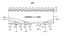
図8は、実施の形態2による光電変換素子の構成を示す断面図である。図8を参照して、実施の形態2による光電変換素子200は、p型単結晶シリコン基板101と、酸化膜102と、p型非晶質膜103,121〜12m−1と、反射防止膜104と、n型非晶質膜111〜11mと、電極131〜13m,141〜14m−1とを備える。
[Embodiment 2]
FIG. 8 is a cross-sectional view showing the configuration of the photoelectric conversion element according to the second embodiment. Referring to FIG. 8, the photoelectric conversion element 200 according to the second embodiment includes a p-type single crystal silicon substrate 101, an oxide film 102, p-type amorphous films 103, 121 to 12m-1, and an antireflection film. 104, n-type amorphous films 111 to 11m, and electrodes 131 to 13m and 141 to 14m-1.

p型単結晶シリコン基板101は、例えば、(100)の面方位および0.1〜1.0Ω・cmの比抵抗を有する。また、p型単結晶シリコン基板101は、例えば、100〜300μmの厚みを有し、好ましくは、100〜200μmの厚みを有する。更に、p型単結晶シリコン基板101は、光入射側の表面がテクスチャ化されている。   The p-type single crystal silicon substrate 101 has, for example, a (100) plane orientation and a specific resistance of 0.1 to 1.0 Ω · cm. The p-type single crystal silicon substrate 101 has a thickness of 100 to 300 μm, for example, and preferably has a thickness of 100 to 200 μm. Furthermore, the p-type single crystal silicon substrate 101 has a textured surface on the light incident side.

酸化膜102は、例えば、SiOからなり、p型単結晶シリコン基板101の光入射側の表面に接して設けられる。そして、酸化膜102は、例えば、数nmの膜厚を有する。 The oxide film 102 is made of, for example, SiO 2 and is provided in contact with the light incident side surface of the p-type single crystal silicon substrate 101. The oxide film 102 has a film thickness of several nm, for example.

p型非晶質膜103は、非晶質相からなり、例えば、p型a−Siからなる。また、p型非晶質膜103は、例えば、10nm〜数十nmの膜厚を有する。更に、p型非晶質層103のB濃度は、1×1018cm−3〜1×1020cm−3である。そして、p型非晶質膜103は、酸化膜102に接して形成される。 The p-type amorphous film 103 is made of an amorphous phase, for example, p-type a-Si. The p-type amorphous film 103 has a thickness of 10 nm to several tens of nm, for example. Furthermore, the B concentration of the p-type amorphous layer 103 is 1 × 10 18 cm −3 to 1 × 10 20 cm −3 . The p-type amorphous film 103 is formed in contact with the oxide film 102.

反射防止膜104は、例えば、Siからなり、膜厚は、例えば、100nmである。そして、反射防止膜104は、p型非晶質膜103に接して設けられる。 The antireflection film 104 is made of, for example, Si 3 N 4 and has a film thickness of, for example, 100 nm. The antireflection film 104 is provided in contact with the p-type amorphous film 103.

n型非晶質膜111〜11mの各々は、非晶質相からなり、p型単結晶シリコン基板101の光入射側と反対側の表面に接して設けられる。そして、n型非晶質膜111〜11mの各々は、例えば、n型a−Siからなり、膜厚は、例えば、10nmである。また、n型非晶質膜111〜11mは、p型単結晶シリコン基板101の面内方向において所望の間隔で配置される。更に、n型非晶質膜111〜11mの各々におけるP濃度は、例えば、5×1019cm−3である。 Each of n-type amorphous films 111 to 11m is made of an amorphous phase, and is provided in contact with the surface of p-type single crystal silicon substrate 101 opposite to the light incident side. Each of the n-type amorphous films 111 to 11m is made of, for example, n-type a-Si and has a film thickness of, for example, 10 nm. The n-type amorphous films 111 to 11m are arranged at a desired interval in the in-plane direction of the p-type single crystal silicon substrate 101. Furthermore, the P concentration in each of the n-type amorphous films 111 to 11m is, for example, 5 × 10 19 cm −3 .

p型非晶質膜121〜12m−1の各々は、非晶質相からなる。p型非晶質膜121は、n型非晶質膜111,112およびp型単結晶シリコン基板101に接して配置され、p型非晶質膜122は、n型非晶質膜112,113およびp型単結晶シリコン基板101に接して配置され、以下、同様にして、p型非晶質膜12m−1は、n型非晶質膜11m−1,11mおよびp型単結晶シリコン基板101に接して配置される。   Each of the p-type amorphous films 121 to 12m-1 is made of an amorphous phase. The p-type amorphous film 121 is disposed in contact with the n-type amorphous films 111 and 112 and the p-type single crystal silicon substrate 101, and the p-type amorphous film 122 is composed of the n-type amorphous films 112 and 113. In the same manner, the p-type amorphous film 12m-1 is divided into the n-type amorphous films 11m-1 and 11m and the p-type single crystal silicon substrate 101. It is arranged in contact with.

そして、p型非晶質膜121〜12m−1の各々は、例えば、p型a−Siからなり、膜厚は、例えば、10nmである。また、p型非晶質膜121〜12m−1の各々におけるB濃度は、例えば、5×1019cm−3である。 Each of the p-type amorphous films 121 to 12m−1 is made of, for example, p-type a-Si, and has a film thickness of, for example, 10 nm. Further, the B concentration in each of the p-type amorphous films 121 to 12m−1 is, for example, 5 × 10 19 cm −3 .

電極131〜13mは、それぞれ、n型非晶質膜111〜11mに接して設けられる。電極141〜14m−1は、それぞれ、p型非晶質膜121〜12m−1に接して設けられる。そして、電極131〜13m,141〜14m−1の各々は、例えば、Agからなる。   The electrodes 131 to 13m are provided in contact with the n-type amorphous films 111 to 11m, respectively. The electrodes 141 to 14m-1 are provided in contact with the p-type amorphous films 121 to 12m-1, respectively. And each of the electrodes 131-13m and 141-14m-1 consists of Ag, for example.

n型非晶質膜111〜11mおよびp型非晶質膜121〜12m−1は、図8の紙面に垂直な方向において同じ長さを有する。そして、n型非晶質膜111〜11mの全体の面積がp型単結晶シリコン基板101の面積に占める割合である面積占有率は、60〜93%であり、p型非晶質膜121〜12m−1の全体の面積がp型単結晶シリコン基板101の面積に占める割合である面積占有率は、5〜20%である。   The n-type amorphous films 111 to 11m and the p-type amorphous films 121 to 12m-1 have the same length in the direction perpendicular to the paper surface of FIG. The area occupation ratio, which is the ratio of the entire area of the n-type amorphous films 111 to 11m to the area of the p-type single crystal silicon substrate 101, is 60 to 93%. The area occupation ratio, which is the ratio of the entire area of 12m−1 to the area of the p-type single crystal silicon substrate 101, is 5 to 20%.

このように、n型非晶質膜111〜11mの面積占有率をp型非晶質膜121〜12m−1の面積占有率よりも大きくするのは、p型単結晶シリコン基板101中で光励起された電子および正孔がpn接合(n型非晶質膜111〜11m/p型単結晶シリコン基板101)によって分離され易くし、光励起された電子および正孔の発電への寄与率を高くするためである。   As described above, the area occupation ratio of the n-type amorphous films 111 to 11m is made larger than the area occupation ratio of the p-type amorphous films 121 to 12m-1 in the p-type single crystal silicon substrate 101. The separated electrons and holes are easily separated by the pn junction (n-type amorphous film 111-11m / p-type single crystal silicon substrate 101), and the contribution rate of photoexcited electrons and holes to power generation is increased. Because.

光電変換素子200は、図2から図4に示す工程(a)〜工程(l)に従って製造される。この場合、n型単結晶シリコン基板1、酸化膜2、n型非晶質膜3、反射防止膜4、p型非晶質膜11〜1m、n型非晶質膜21〜2m−1および電極31〜3m,41〜4m−1をそれぞれp型単結晶シリコン基板101、酸化膜102、p型非晶質膜103、反射防止膜104、n型非晶質膜111〜11m、p型非晶質膜121〜12m−1および電極131〜13m,141〜14m−1に読み替えればよい。そして、酸化膜102は、酸化膜2と同じ方法によって形成され、p型非晶質膜103,121〜12m−1は、表1に示すp型非晶質膜11〜1mと同じ材料ガスおよびp型非晶質膜11〜1mの条件と同じ条件を用いてプラズマCVD法によって形成される。n型非晶質膜111〜11mは、表1に示すn型非晶質膜21〜2m−1と同じ材料ガスおよびn型非晶質膜21〜2m−1の条件と同じ条件を用いてプラズマCVD法によって形成される。また、反射防止膜104は、反射防止膜4と同じ方法によって形成される。   The photoelectric conversion element 200 is manufactured according to the steps (a) to (l) shown in FIGS. In this case, n-type single crystal silicon substrate 1, oxide film 2, n-type amorphous film 3, antireflection film 4, p-type amorphous films 11-1m, n-type amorphous films 21-2m-1, and The electrodes 31 to 3m and 41 to 4m−1 are respectively connected to the p-type single crystal silicon substrate 101, the oxide film 102, the p-type amorphous film 103, the antireflection film 104, the n-type amorphous films 111 to 11m, and the p-type non-electrode. What is necessary is just to read as crystalline film 121-12m-1, electrode 131-13m, 141-14m-1. The oxide film 102 is formed by the same method as the oxide film 2, and the p-type amorphous films 103 and 121-12m-1 are made of the same material gas and p-type amorphous films 11-1m shown in Table 1. It is formed by the plasma CVD method using the same conditions as those for the p-type amorphous films 11 to 1m. The n-type amorphous films 111 to 11m are formed using the same material gas as the n-type amorphous films 21 to 2m-1 shown in Table 1 and the same conditions as the conditions of the n-type amorphous films 21 to 2m-1. It is formed by a plasma CVD method. The antireflection film 104 is formed by the same method as the antireflection film 4.

光電変換素子200において、太陽光が反射防止膜104側から光電変換素子200に照射されると、p型単結晶シリコン基板101中で電子および正孔が光励起される。   In the photoelectric conversion element 200, when sunlight is irradiated onto the photoelectric conversion element 200 from the antireflection film 104 side, electrons and holes are photoexcited in the p-type single crystal silicon substrate 101.

光励起された電子および正孔は、酸化膜102側へ拡散しても、酸化膜102によるp型単結晶シリコン基板101のパッシベーション効果およびp型非晶質膜103によるFSF効果(表面電界効果)によって再結合し難くなり、n型非晶質膜111〜11mおよびp型非晶質膜121〜12m−1側へ拡散し易くなる。   Even if the photoexcited electrons and holes diffuse to the oxide film 102 side, the passivation effect of the p-type single crystal silicon substrate 101 by the oxide film 102 and the FSF effect (surface electric field effect) by the p-type amorphous film 103 It becomes difficult to recombine, and it becomes easy to diffuse to the n-type amorphous films 111 to 11m and the p-type amorphous films 121 to 12m-1.

より具体的には、p型単結晶シリコン基板101のテクスチャ化された表面に酸化膜102(=SiO)が接しているので、p型単結晶シリコン基板101と酸化膜102(=SiO)との界面における界面準位密度は、1010cm−2〜1011cm−2と非常に低い。その結果、キャリア(電子および正孔)は、p型単結晶シリコン基板101のテクスチャ化された表面において殆ど再結合しない。また、酸化膜102の膜厚は、上述したように数nmであるので、キャリア(電子および正孔)は、p型非晶質膜103によるFSF効果によってp型単結晶シリコン基板101と酸化膜102との界面へ到達し難くなり、再結合が更に抑制される。特に、少数キャリアである電子の再結合が抑制される。即ち、p型非晶質膜103を構成するp型a−Siの光学バンドギャップ(=約1.7eV)および活性化エネルギー(=約0.3eV〜0.4eV)とp型単結晶シリコン基板101の光学バンドギャップ(=1.1eV)および活性化エネルギー(=0.2eV〜0.3eV)とを考慮すると、p型a−Siの伝導帯の端は、p型単結晶シリコン基板101の伝導帯の端よりも、0.4eV〜0.6eVだけ高エネルギー側に存在するので、p型非晶質膜103は、p型単結晶シリコン基板101の表面近傍において表面電界を発生する。その結果、p型単結晶シリコン基板101の表面近傍へ拡散した電子は、p型非晶質膜103による表面電界によってp型単結晶シリコン基板101と酸化膜102との界面へ到達し難くなる。従って、少数キャリアである電子の再結合がFSF効果によって抑制される。 More specifically, since the oxide film 102 (= SiO 2 ) is in contact with the textured surface of the p-type single crystal silicon substrate 101, the p-type single crystal silicon substrate 101 and the oxide film 102 (= SiO 2 ) The interface state density at the interface is very low, 10 10 cm −2 to 10 11 cm −2 . As a result, carriers (electrons and holes) hardly recombine on the textured surface of the p-type single crystal silicon substrate 101. Since the thickness of the oxide film 102 is several nm as described above, carriers (electrons and holes) are separated from the p-type single crystal silicon substrate 101 and the oxide film by the FSF effect of the p-type amorphous film 103. It becomes difficult to reach the interface with 102, and recombination is further suppressed. In particular, recombination of electrons that are minority carriers is suppressed. That is, the optical band gap (= about 1.7 eV) and activation energy (= about 0.3 eV to 0.4 eV) of p-type a-Si constituting the p-type amorphous film 103 and the p-type single crystal silicon substrate When the optical band gap (= 1.1 eV) and activation energy (= 0.2 eV to 0.3 eV) of 101 are taken into consideration, the end of the p-type a-Si conduction band corresponds to the p-type single crystal silicon substrate 101. The p-type amorphous film 103 generates a surface electric field in the vicinity of the surface of the p-type single crystal silicon substrate 101 because it exists on the high energy side by 0.4 eV to 0.6 eV from the end of the conduction band. As a result, electrons diffused near the surface of the p-type single crystal silicon substrate 101 are unlikely to reach the interface between the p-type single crystal silicon substrate 101 and the oxide film 102 due to the surface electric field generated by the p-type amorphous film 103. Therefore, recombination of electrons that are minority carriers is suppressed by the FSF effect.

このように、キャリア(電子および正孔)は、酸化膜102およびp型非晶質膜103によってp型単結晶シリコン基板101の表面における再結合が抑制され、n型非晶質膜111〜11mおよびp型非晶質膜121〜12m−1側へ拡散し易くなる。   Thus, carriers (electrons and holes) are suppressed from recombination on the surface of the p-type single crystal silicon substrate 101 by the oxide film 102 and the p-type amorphous film 103, and the n-type amorphous films 111 to 11m. And it becomes easy to diffuse to the p-type amorphous films 121 to 12m−1 side.

そして、n型非晶質膜111〜11mおよびp型非晶質膜121〜12m−1側へ拡散した電子および正孔は、n型非晶質膜111〜11m/p型単結晶シリコン基板101(=pn接合)による内部電界によって分離され、電子は、n型非晶質膜111〜11mを介して電極131〜13mへ到達し、正孔は、p型非晶質膜121〜12m−1を介して電極141〜14m−1へ到達する。   Then, the electrons and holes diffused toward the n-type amorphous films 111 to 11m and the p-type amorphous films 121 to 12m-1 are transferred to the n-type amorphous films 111 to 11m / p-type single crystal silicon substrate 101. The electrons are separated by the internal electric field due to (= pn junction), the electrons reach the electrodes 131 to 13m through the n-type amorphous films 111 to 11m, and the holes are the p-type amorphous films 121 to 12m-1. To reach the electrodes 141-14m-1.

電極131〜13mへ到達した電子は、電極131〜13mと電極141〜14m−1との間に接続された負荷を介して電極141〜14m−1へ到達し、正孔と再結合する。   The electrons that have reached the electrodes 131 to 13m reach the electrodes 141 to 14m-1 via a load connected between the electrodes 131 to 13m and the electrodes 141 to 14m-1, and recombine with the holes.

このように、光電変換素子200は、p型単結晶シリコン基板101中で光励起された電子および正孔をp型単結晶シリコン基板101の裏面(=酸化膜102が形成されたp型単結晶シリコン基板101の表面と反対側の面)から取り出すバックコンタクト型の光電変換素子である。   In this way, the photoelectric conversion element 200 converts electrons and holes photoexcited in the p-type single crystal silicon substrate 101 into the back surface of the p-type single crystal silicon substrate 101 (= p-type single crystal silicon on which the oxide film 102 is formed). This is a back-contact photoelectric conversion element that is taken out from the surface opposite to the surface of the substrate 101.

そして、光電変換素子200は、光入射側に、酸化膜102およびp型非晶質膜103を備えるので、上述したように、p型単結晶シリコン基板101に対するパッシベーション効果を向上できる。   Since the photoelectric conversion element 200 includes the oxide film 102 and the p-type amorphous film 103 on the light incident side, the passivation effect on the p-type single crystal silicon substrate 101 can be improved as described above.

また、光電変換素子100において説明したように、光電変換素子200の製造工程において、p型単結晶シリコン基板101の受光面側の表面を保護できる。   Further, as described in the photoelectric conversion element 100, the surface on the light receiving surface side of the p-type single crystal silicon substrate 101 can be protected in the manufacturing process of the photoelectric conversion element 200.

図9は、実施の形態2による他の光電変換素子の構成を示す断面図である。実施の形態2による光電変換素子は、図9に示す光電変換素子200Aであってもよい。   FIG. 9 is a cross-sectional view showing a configuration of another photoelectric conversion element according to the second embodiment. The photoelectric conversion element according to Embodiment 2 may be a photoelectric conversion element 200A shown in FIG.

図9を参照して、光電変換素子200Aは、図8に示す光電変換素子200にi型非晶質膜151〜15mを追加したものであり、その他は、光電変換素子200と同じである。   Referring to FIG. 9, a photoelectric conversion element 200 </ b> A is obtained by adding i-type amorphous films 151 to 15 m to the photoelectric conversion element 200 illustrated in FIG. 8, and is otherwise the same as the photoelectric conversion element 200.

i型非晶質膜151〜15mは、非晶質相からなり、それぞれ、p型単結晶シリコン基板101およびn型非晶質膜111〜11mに接し、p型単結晶シリコン基板101とn型非晶質膜111〜11mとの間に配置される。そして、i型非晶質膜151〜15mの各々は、例えば、i型a−Siからなり、膜厚は、例えば、10nmである。また、i型非晶質膜151〜15mは、p型単結晶シリコン基板101の面内方向(図9の紙面における左右方向)において、それぞれ、n型非晶質膜111〜11mと同じ幅を有する。更に、i型非晶質膜151〜15mは、図9の紙面に垂直な方向において、それぞれ、n型非晶質膜111〜11mと同じ長さを有する。   The i-type amorphous films 151 to 15m are made of an amorphous phase and are in contact with the p-type single crystal silicon substrate 101 and the n-type amorphous films 111 to 11m, respectively. It arrange | positions between the amorphous | non-crystalline films 111-11m. Each of the i-type amorphous films 151 to 15m is made of, for example, i-type a-Si, and has a film thickness of, for example, 10 nm. Further, the i-type amorphous films 151 to 15m have the same width as the n-type amorphous films 111 to 11m in the in-plane direction of the p-type single crystal silicon substrate 101 (the left-right direction in the paper surface of FIG. 9), respectively. Have. Furthermore, the i-type amorphous films 151 to 15m have the same length as the n-type amorphous films 111 to 11m, respectively, in the direction perpendicular to the paper surface of FIG.

光電変換素子200Aにおいては、p型非晶質膜121〜12m−1の各々の膜厚は、n型非晶質膜111〜11mの膜厚とi型非晶質膜151〜15mの膜厚との合計膜厚からなる。   In the photoelectric conversion element 200A, the thicknesses of the p-type amorphous films 121 to 12m−1 are the thicknesses of the n-type amorphous films 111 to 11m and the i-type amorphous films 151 to 15m, respectively. And the total film thickness.

また、光電変換素子200Aにおいては、i型非晶質膜151の端面は、p型非晶質膜121に接し、i型非晶質膜152の端面は、p型非晶質膜121,122に接し、i型非晶質膜153の端面は、p型非晶質膜122,123に接し、以下、同様にして、i型非晶質膜15m−1の端面は、p型非晶質膜12m−2,12m−1に接し、i型非晶質膜15mの端面は、p型非晶質膜12m−1に接する。   In the photoelectric conversion element 200A, the end surface of the i-type amorphous film 151 is in contact with the p-type amorphous film 121, and the end surface of the i-type amorphous film 152 is the p-type amorphous film 121, 122. The end surface of the i-type amorphous film 153 is in contact with the p-type amorphous films 122 and 123. Similarly, the end surface of the i-type amorphous film 15m-1 is the p-type amorphous film. The end faces of the i-type amorphous film 15m are in contact with the p-type amorphous film 12m-1 in contact with the films 12m-2 and 12m-1.

光電変換素子200Aは、図2〜図4に示す工程(a)〜工程(l)によって製造される。この場合、図2の工程(d)において、i型非晶質膜151〜15m用のi型非晶質膜がプラズマCVD法によってp型単結晶シリコン基板101上に堆積され、その後、n型非晶質膜111〜11m用のn型非晶質膜がプラズマCVD法によってi型非晶質膜151〜15m用のi型非晶質膜上に堆積される。そして、i型非晶質膜151〜15m用のi型非晶質膜を堆積するときのガス流量は、表1に示すi型非晶質膜51〜5mのガス流量と同じであり、n型非晶質膜111〜11m用のn型非晶質膜を堆積するときのガス流量は、表1に示すn型非晶質膜21〜2m−1のガス流量と同じである。   200 A of photoelectric conversion elements are manufactured by the process (a)-process (l) shown in FIGS. In this case, in the step (d) of FIG. 2, an i-type amorphous film for the i-type amorphous films 151 to 15m is deposited on the p-type single crystal silicon substrate 101 by the plasma CVD method. An n-type amorphous film for the amorphous films 111 to 11m is deposited on the i-type amorphous film for the i-type amorphous films 151 to 15m by a plasma CVD method. The gas flow rate when depositing the i-type amorphous film for the i-type amorphous films 151 to 15m is the same as the gas flow rate of the i-type amorphous films 51 to 5m shown in Table 1, and n The gas flow rate when depositing the n-type amorphous film for the n-type amorphous films 111 to 11m is the same as the gas flow rate of the n-type amorphous films 21 to 2m-1 shown in Table 1.

光電変換素子200Aにおける発電機構は、光電変換素子200の発電機構と概ね同じであり、光電変換素子200において説明したように、電子および正孔は、p型単結晶シリコン基板101の光入射側の表面(テクスチャ化された表面)における再結合が抑制され、n型非晶質膜111〜11mおよびp型非晶質膜121〜12m−1側へ拡散し易くなる。そして、n型非晶質膜111〜11mおよびp型非晶質膜121〜12m−1側へ拡散した電子および正孔は、n型非晶質膜111〜11m/i型非晶質膜151〜15m/p型単結晶シリコン基板101(=pin接合)による内部電界によって分離され、電子は、i型非晶質膜151〜15mおよびn型非晶質膜111〜11mを介して電極131〜13mへ到達し、正孔は、p型非晶質膜121〜12m−1を介して電極141〜14m−1へ到達する。   The power generation mechanism in the photoelectric conversion element 200 </ b> A is substantially the same as the power generation mechanism of the photoelectric conversion element 200, and as described in the photoelectric conversion element 200, electrons and holes are on the light incident side of the p-type single crystal silicon substrate 101. Recombination on the surface (textured surface) is suppressed, and diffusion to the n-type amorphous films 111 to 11m and p-type amorphous films 121 to 12m-1 side is facilitated. The electrons and holes diffused toward the n-type amorphous films 111 to 11m and the p-type amorphous films 121 to 12m-1 are converted into the n-type amorphous films 111 to 11m / i-type amorphous film 151. ~ 15m / p type single crystal silicon substrate 101 (= pin junction) is separated by an internal electric field, and electrons are separated from the electrodes 131 through the i-type amorphous films 151 to 15m and the n-type amorphous films 111 to 11m. The holes reach 13m, and the holes reach the electrodes 141-14m-1 through the p-type amorphous films 121-12m-1.

電極131〜13mへ到達した電子は、電極131〜13mと電極141〜14m−1との間に接続された負荷を介して電極141〜14m−1へ到達し、正孔と再結合する。   The electrons that have reached the electrodes 131 to 13m reach the electrodes 141 to 14m-1 via a load connected between the electrodes 131 to 13m and the electrodes 141 to 14m-1, and recombine with the holes.

このように、光電変換素子200Aは、p型単結晶シリコン基板101中で光励起された電子および正孔をp型単結晶シリコン基板101の裏面(=酸化膜102が形成されたp型単結晶シリコン基板101の表面と反対側の面)から取り出すバックコンタクト型の光電変換素子である。   As described above, the photoelectric conversion element 200A allows electrons and holes photoexcited in the p-type single crystal silicon substrate 101 to be transferred to the back surface of the p-type single crystal silicon substrate 101 (= p-type single crystal silicon on which the oxide film 102 is formed). This is a back-contact photoelectric conversion element that is taken out from the surface opposite to the surface of the substrate 101.

そして、光電変換素子200Aは、p型単結晶シリコン基板101の光入射側の表面(テクスチャ化された表面)に接して設けられた酸化膜102と、酸化膜102に接して設けられたp型非晶質膜103とを備えるので、光電変換素子200において説明したように、p型単結晶シリコン基板101に対するパッシベーション効果を向上できる。   The photoelectric conversion element 200A includes an oxide film 102 provided in contact with the light incident surface (textured surface) of the p-type single crystal silicon substrate 101, and a p-type provided in contact with the oxide film 102. Since the amorphous film 103 is provided, the passivation effect on the p-type single crystal silicon substrate 101 can be improved as described in the photoelectric conversion element 200.

また、光電変換素子200Aにおいては、p型単結晶シリコン基板101とn型非晶質膜111〜11mとの間にi型非晶質膜151〜15mが存在するので、p型単結晶シリコン基板101とn型非晶質膜111〜11mとの界面における電子の再結合が抑制される。その結果、短絡光電流が増加し、光電変換素子200Aの変換効率を向上できる。   In the photoelectric conversion element 200A, since the i-type amorphous films 151 to 15m exist between the p-type single crystal silicon substrate 101 and the n-type amorphous films 111 to 11m, the p-type single crystal silicon substrate Recombination of electrons at the interface between 101 and the n-type amorphous films 111 to 11m is suppressed. As a result, the short-circuit photocurrent increases and the conversion efficiency of the photoelectric conversion element 200A can be improved.

光電変換素子200Aについてのその他の説明は、光電変換素子200についての説明と同じである。   The other description of the photoelectric conversion element 200A is the same as the description of the photoelectric conversion element 200.

図10は、実施の形態2による更に他の光電変換素子の構成を示す断面図である。実施の形態2による光電変換素子は、図10に示す光電変換素子200Bであってもよい。   FIG. 10 is a cross-sectional view illustrating a configuration of still another photoelectric conversion element according to the second embodiment. The photoelectric conversion element according to Embodiment 2 may be a photoelectric conversion element 200B shown in FIG.

図10を参照して、光電変換素子200Bは、図8に示す光電変換素子200にi型非晶質膜161〜16m−1を追加したものであり、その他は、光電変換素子200と同じである。   Referring to FIG. 10, photoelectric conversion element 200B is obtained by adding i-type amorphous films 161 to 16m-1 to photoelectric conversion element 200 shown in FIG. is there.

i型非晶質膜161〜16m−1は、非晶質相からなり、それぞれ、p型単結晶シリコン基板101およびp型非晶質膜121〜12m−1に接し、p型単結晶シリコン基板101とp型非晶質膜121〜12m−1との間に配置される。そして、i型非晶質膜161〜16m−1の各々は、例えば、i型a−Siからなり、膜厚は、例えば、10nmである。また、i型非晶質膜161〜16m−1は、図10の紙面に垂直な方向において、それぞれ、p型非晶質膜121〜12m−1と同じ長さを有する。   The i-type amorphous films 161 to 16m-1 are made of an amorphous phase and are in contact with the p-type single crystal silicon substrate 101 and the p-type amorphous films 121 to 12m-1, respectively. 101 and the p-type amorphous films 121 to 12m-1. Each of the i-type amorphous films 161 to 16m-1 is made of, for example, i-type a-Si and has a film thickness of, for example, 10 nm. The i-type amorphous films 161 to 16m-1 have the same length as the p-type amorphous films 121 to 12m-1 in the direction perpendicular to the paper surface of FIG.

光電変換素子200Bにおいては、n型非晶質膜111〜11mの各々の膜厚は、p型非晶質膜121〜12m−1の膜厚とi型非晶質膜161〜16m−1の膜厚との合計膜厚からなる。   In the photoelectric conversion element 200B, each of the n-type amorphous films 111 to 11m has a thickness of the p-type amorphous films 121 to 12m-1 and that of the i-type amorphous films 161 to 16m-1. It consists of the total film thickness with the film thickness.

また、光電変換素子200Bにおいては、n型非晶質膜111の端面は、i型非晶質膜161およびp型非晶質膜121に接し、n型非晶質膜112の端面は、i型非晶質膜161およびp型非晶質膜121とi型非晶質膜162およびp型非晶質膜122とに接し、n型非晶質膜113の端面は、i型非晶質膜162およびp型非晶質膜122とi型非晶質膜163およびp型非晶質膜123とに接し、以下、同様にして、n型非晶質膜11m−1の端面は、i型非晶質膜16m−2およびp型非晶質膜12m−2とi型非晶質膜16m−1およびp型非晶質膜12m−1とに接し、n型非晶質膜11mの端面は、i型非晶質膜16m−1およびp型非晶質膜12m−1に接する。   In the photoelectric conversion element 200B, the end surface of the n-type amorphous film 111 is in contact with the i-type amorphous film 161 and the p-type amorphous film 121, and the end surface of the n-type amorphous film 112 is i. The end face of the n-type amorphous film 113 is in contact with the i-type amorphous film 161 and the p-type amorphous film 121 and the i-type amorphous film 162 and the p-type amorphous film 122. The end face of the n-type amorphous film 11m-1 is in contact with the film 162 and the p-type amorphous film 122, the i-type amorphous film 163 and the p-type amorphous film 123. The n-type amorphous film 11m is in contact with the n-type amorphous film 16m-2 and the p-type amorphous film 12m-2 and the i-type amorphous film 16m-1 and the p-type amorphous film 12m-1. The end face is in contact with the i-type amorphous film 16m-1 and the p-type amorphous film 12m-1.

光電変換素子200Bは、図2〜図4に示す工程(a)〜工程(l)によって製造される。この場合、図3の工程(i)において、i型非晶質膜161〜16m−1用のi型非晶質膜がプラズマCVD法によってp型単結晶シリコン基板101およびn型非晶質膜111〜11m上に堆積され、その後、p型非晶質膜121〜12m−1用のp型非晶質膜がプラズマCVD法によってi型非晶質膜161〜16m−1用のi型非晶質膜上に堆積される。そして、i型非晶質膜161〜16m−1用のi型非晶質膜を堆積するときのガス流量は、表1に示すi型非晶質膜51〜5mのガス流量と同じであり、p型非晶質膜121〜12m−1用のp型非晶質膜を堆積するときのガス流量は、表1に示すp型非晶質膜11〜1mのガス流量と同じである。   The photoelectric conversion element 200B is manufactured by steps (a) to (l) illustrated in FIGS. In this case, in step (i) of FIG. 3, the i-type amorphous films for the i-type amorphous films 161 to 16m-1 are converted into the p-type single crystal silicon substrate 101 and the n-type amorphous film by the plasma CVD method. Then, the p-type amorphous film for the p-type amorphous films 121 to 12m-1 is deposited on the i-type amorphous films 161 to 16m-1 by the plasma CVD method. Deposited on the crystalline film. The gas flow rate when depositing the i-type amorphous film for the i-type amorphous film 161 to 16m-1 is the same as the gas flow rate of the i-type amorphous film 51 to 5m shown in Table 1. The gas flow rate when depositing the p-type amorphous film for the p-type amorphous films 121 to 12m-1 is the same as the gas flow rate of the p-type amorphous films 11 to 1m shown in Table 1.

光電変換素子200Bにおける発電機構は、光電変換素子200の発電機構と概ね同じであり、光電変換素子200において説明したように、電子および正孔は、p型単結晶シリコン基板101の光入射側の表面(テクスチャ化された表面)における再結合が抑制され、n型非晶質膜111〜11mおよびp型非晶質膜121〜12m−1側へ拡散し易くなる。そして、n型非晶質膜111〜11mおよびp型非晶質膜121〜12m−1側へ拡散した電子および正孔は、n型非晶質膜111〜11m/p型単結晶シリコン基板101(=pn接合)による内部電界によって分離され、電子は、n型非晶質膜111〜11mを介して電極131〜13mへ到達し、正孔は、i型非晶質膜161〜16m−1およびp型非晶質膜121〜12m−1を介して電極141〜14m−1へ到達する。   The power generation mechanism in the photoelectric conversion element 200B is substantially the same as the power generation mechanism in the photoelectric conversion element 200. As described in the photoelectric conversion element 200, electrons and holes are generated on the light incident side of the p-type single crystal silicon substrate 101. Recombination on the surface (textured surface) is suppressed, and diffusion to the n-type amorphous films 111 to 11m and p-type amorphous films 121 to 12m-1 side is facilitated. Then, the electrons and holes diffused toward the n-type amorphous films 111 to 11m and the p-type amorphous films 121 to 12m-1 are transferred to the n-type amorphous films 111 to 11m / p-type single crystal silicon substrate 101. (= Pn junction) is separated by an internal electric field, electrons reach the electrodes 131 to 13m via the n-type amorphous films 111 to 11m, and the holes are i-type amorphous films 161 to 16m-1. And it reaches the electrodes 141-14m-1 through the p-type amorphous films 121-12m-1.

電極131〜13m−1へ到達した電子は、電極131〜13m−1と電極141〜14m−1との間に接続された負荷を介して電極141〜14m−1へ到達し、正孔と再結合する。   The electrons that have reached the electrodes 131 to 13m-1 reach the electrodes 141 to 14m-1 via a load connected between the electrodes 131 to 13m-1 and the electrodes 141 to 14m-1, and are regenerated with holes. Join.

このように、光電変換素子200Bは、p型単結晶シリコン基板101中で光励起された電子および正孔をp型単結晶シリコン基板101の裏面(=酸化膜102が形成されたp型単結晶シリコン基板101の表面と反対側の面)から取り出すバックコンタクト型の光電変換素子である。   As described above, the photoelectric conversion element 200B converts the electrons and holes photoexcited in the p-type single crystal silicon substrate 101 into the back surface of the p-type single crystal silicon substrate 101 (= p-type single crystal silicon on which the oxide film 102 is formed). This is a back-contact photoelectric conversion element that is taken out from the surface opposite to the surface of the substrate 101.

そして、光電変換素子200Bは、p型単結晶シリコン基板101の光入射側の表面(テクスチャ化された表面)に接して設けられた酸化膜102と、酸化膜102に接して設けられたp型非晶質膜103とを備えるので、光電変換素子200において説明したように、p型単結晶シリコン基板101に対するパッシベーション効果を向上できる。   The photoelectric conversion element 200B includes an oxide film 102 provided in contact with the light incident surface (textured surface) of the p-type single crystal silicon substrate 101, and a p-type provided in contact with the oxide film 102. Since the amorphous film 103 is provided, the passivation effect on the p-type single crystal silicon substrate 101 can be improved as described in the photoelectric conversion element 200.

また、光電変換素子200Bにおいては、p型単結晶シリコン基板101とp型非晶質膜121〜12m−1との間にi型非晶質膜161〜16m−1が存在するので、p型単結晶シリコン基板101とp型非晶質膜121〜12m−1との界面における正孔の再結合が抑制される。その結果、短絡光電流が増加し、光電変換素子200Bの変換効率を向上できる。   In the photoelectric conversion element 200B, since the i-type amorphous films 161 to 16m-1 exist between the p-type single crystal silicon substrate 101 and the p-type amorphous films 121 to 12m-1, the p-type Recombination of holes at the interface between the single crystal silicon substrate 101 and the p-type amorphous films 121 to 12m−1 is suppressed. As a result, the short-circuit photocurrent increases and the conversion efficiency of the photoelectric conversion element 200B can be improved.

光電変換素子200Bについてのその他の説明は、光電変換素子200についての説明と同じである。   The other description of the photoelectric conversion element 200B is the same as the description of the photoelectric conversion element 200.

図11は、実施の形態2による更に他の光電変換素子の構成を示す断面図である。実施の形態2による光電変換素子は、図11に示す光電変換素子200Cであってもよい。   FIG. 11 is a cross-sectional view illustrating a configuration of still another photoelectric conversion element according to the second embodiment. The photoelectric conversion element according to Embodiment 2 may be a photoelectric conversion element 200C shown in FIG.

図11を参照して、光電変換素子200Cは、図8に示す光電変換素子200にi型非晶質膜151〜15m,161〜16m−1を追加したものであり、その他は、光電変換素子200と同じである。   Referring to FIG. 11, a photoelectric conversion element 200C is obtained by adding i-type amorphous films 151 to 15m and 161 to 16m-1 to the photoelectric conversion element 200 shown in FIG. The same as 200.

i型非晶質膜151〜15m,161〜16m−1については、上述したとおりである。   The i-type amorphous films 151 to 15m and 161 to 16m-1 are as described above.

光電変換素子200Cにおいては、i型非晶質膜161の端面は、i型非晶質膜151,152に接し、i型非晶質膜162の端面は、i型非晶質膜152,153に接し、以下、同様にして、i型非晶質膜16m−1の端面は、i型非晶質膜15m−1,15mに接する。また、p型非晶質膜121の端面は、n型非晶質膜111,112に接し、p型非晶質膜122の端面は、n型非晶質膜112,113に接し、以下、同様にして、p型非晶質膜12m−1の端面は、n型非晶質膜11m−1,11mに接する。   In the photoelectric conversion element 200C, the end face of the i-type amorphous film 161 is in contact with the i-type amorphous films 151 and 152, and the end face of the i-type amorphous film 162 is the i-type amorphous films 152 and 153. Hereinafter, similarly, the end face of the i-type amorphous film 16m-1 is in contact with the i-type amorphous films 15m-1 and 15m. The end face of the p-type amorphous film 121 is in contact with the n-type amorphous films 111 and 112, and the end face of the p-type amorphous film 122 is in contact with the n-type amorphous films 112 and 113. Similarly, the end face of the p-type amorphous film 12m-1 is in contact with the n-type amorphous films 11m-1 and 11m.

光電変換素子200Cは、図2〜図4に示す工程(a)〜工程(l)によって製造される。この場合、図2の工程(d)において、i型非晶質膜151〜15m用のi型非晶質膜がプラズマCVD法によってp型単結晶シリコン基板101上に堆積され、その後、n型非晶質膜111〜11m用のn型非晶質膜がプラズマCVD法によってi型非晶質膜151〜15m用のi型非晶質膜上に堆積される。また、図3の工程(i)において、i型非晶質膜161〜16m−1用のi型非晶質膜がプラズマCVD法によってp型単結晶シリコン基板101およびn型非晶質膜111〜11m上に堆積され、その後、p型非晶質膜121〜12m−1用のp型非晶質膜がプラズマCVD法によってi型非晶質膜161〜16m−1用のi型非晶質膜上に堆積される。そして、i型非晶質膜151〜15m用のi型非晶質膜と、i型非晶質膜161〜16m−1用のi型非晶質膜とを堆積するときのガス流量は、表1に示すi型非晶質膜51〜5mを堆積するときのガス流量と同じであり、n型非晶質膜111〜11m用のn型非晶質膜を堆積するときのガス流量は、表1に示すn型非晶質膜21〜2m−1を堆積するときのガス流量と同じであり、p型非晶質膜121〜12m−1用のp型非晶質膜を堆積するときのガス流量は、表1に示すp型非晶質膜11〜1mを堆積するときのガス流量と同じである。   The photoelectric conversion element 200C is manufactured by the steps (a) to (l) shown in FIGS. In this case, in the step (d) of FIG. 2, an i-type amorphous film for the i-type amorphous films 151 to 15m is deposited on the p-type single crystal silicon substrate 101 by the plasma CVD method. An n-type amorphous film for the amorphous films 111 to 11m is deposited on the i-type amorphous film for the i-type amorphous films 151 to 15m by a plasma CVD method. Further, in step (i) of FIG. 3, the i-type amorphous films for the i-type amorphous films 161 to 16m-1 are converted into the p-type single crystal silicon substrate 101 and the n-type amorphous film 111 by the plasma CVD method. After that, a p-type amorphous film for the p-type amorphous films 121 to 12m-1 is formed into an i-type amorphous film for the i-type amorphous films 161 to 16m-1 by a plasma CVD method. Deposited on the material film. The gas flow rate when depositing the i-type amorphous film for the i-type amorphous films 151 to 15m and the i-type amorphous film for the i-type amorphous films 161 to 16m-1 is: The gas flow rate when depositing n-type amorphous films for n-type amorphous films 111 to 11m is the same as the gas flow rate when depositing i-type amorphous films 51 to 5m shown in Table 1. The gas flow rate when depositing the n-type amorphous films 21 to 2m-1 shown in Table 1 is the same as that for depositing the p-type amorphous films for the p-type amorphous films 121 to 12m-1. The gas flow rate at that time is the same as the gas flow rate when the p-type amorphous films 11 to 1m shown in Table 1 are deposited.

光電変換素子200Cにおける発電機構は、光電変換素子200の発電機構と概ね同じであり、光電変換素子200において説明したように、電子および正孔は、p型単結晶シリコン基板101の光入射側の表面(テクスチャ化された表面)における再結合が抑制され、n型非晶質膜111〜11mおよびp型非晶質膜121〜12m−1側へ拡散し易くなる。そして、n型非晶質膜111〜11mおよびp型非晶質膜121〜12m−1側へ拡散した電子および正孔は、n型非晶質膜111〜11m/i型非晶質膜151〜15m/p型単結晶シリコン基板101(=pin接合)による内部電界によって分離され、電子は、i型非晶質膜151〜15mおよびn型非晶質膜111〜11mを介して電極131〜13mへ到達し、正孔は、i型非晶質膜161〜16m−1およびp型非晶質膜121〜12m−1を介して電極141〜14m−1へ到達する。   The power generation mechanism in the photoelectric conversion element 200C is substantially the same as the power generation mechanism in the photoelectric conversion element 200. As described in the photoelectric conversion element 200, electrons and holes are generated on the light incident side of the p-type single crystal silicon substrate 101. Recombination on the surface (textured surface) is suppressed, and diffusion to the n-type amorphous films 111 to 11m and p-type amorphous films 121 to 12m-1 side is facilitated. The electrons and holes diffused toward the n-type amorphous films 111 to 11m and the p-type amorphous films 121 to 12m-1 are converted into the n-type amorphous films 111 to 11m / i-type amorphous film 151. ~ 15m / p type single crystal silicon substrate 101 (= pin junction) is separated by an internal electric field, and electrons are separated from the electrodes 131 through the i-type amorphous films 151 to 15m and the n-type amorphous films 111 to 11m. The holes reach 13m, and the holes reach the electrodes 141 to 14m-1 via the i-type amorphous films 161 to 16m-1 and the p-type amorphous films 121 to 12m-1.

電極131〜13mへ到達した電子は、電極131〜13mと電極141〜14m−1との間に接続された負荷を介して電極141〜14m−1へ到達し、正孔と再結合する。   The electrons that have reached the electrodes 131 to 13m reach the electrodes 141 to 14m-1 via a load connected between the electrodes 131 to 13m and the electrodes 141 to 14m-1, and recombine with the holes.

このように、光電変換素子200Cは、p型単結晶シリコン基板101中で光励起された電子および正孔をp型単結晶シリコン基板101の裏面(=酸化膜102が形成されたp型単結晶シリコン基板101の表面と反対側の面)から取り出すバックコンタクト型の光電変換素子である。   As described above, the photoelectric conversion element 200C uses electrons and holes photoexcited in the p-type single crystal silicon substrate 101 to convert the back surface of the p-type single crystal silicon substrate 101 (= p-type single crystal silicon on which the oxide film 102 is formed). This is a back-contact photoelectric conversion element that is taken out from the surface opposite to the surface of the substrate 101.

そして、光電変換素子200Cは、p型単結晶シリコン基板101の光入射側の表面(テクスチャ化された表面)に接して設けられた酸化膜102と、酸化膜102に接して設けられたp型非晶質膜103とを備えるので、光電変換素子200において説明したように、p型単結晶シリコン基板101に対するパッシベーション効果を向上できる。   The photoelectric conversion element 200C includes an oxide film 102 provided in contact with the light incident surface (textured surface) of the p-type single crystal silicon substrate 101, and a p-type provided in contact with the oxide film 102. Since the amorphous film 103 is provided, the passivation effect on the p-type single crystal silicon substrate 101 can be improved as described in the photoelectric conversion element 200.

また、光電変換素子200Cにおいては、p型単結晶シリコン基板101とn型非晶質膜111〜11mとの間にi型非晶質膜151〜15mが存在するので、p型単結晶シリコン基板101とn型非晶質膜111〜11mとの界面における電子の再結合が抑制される。更に、光電変換素子200Cにおいては、p型単結晶シリコン基板101とp型非晶質膜121〜12m−1との間にi型非晶質膜161〜16m−1が存在するので、p型単結晶シリコン基板101とp型非晶質膜121〜12m−1との界面における正孔の再結合が抑制される。   In the photoelectric conversion element 200C, since the i-type amorphous films 151 to 15m exist between the p-type single crystal silicon substrate 101 and the n-type amorphous films 111 to 11m, the p-type single crystal silicon substrate Recombination of electrons at the interface between 101 and the n-type amorphous films 111 to 11m is suppressed. Further, in the photoelectric conversion element 200C, since the i-type amorphous films 161 to 16m-1 exist between the p-type single crystal silicon substrate 101 and the p-type amorphous films 121 to 12m-1, the p-type Recombination of holes at the interface between the single crystal silicon substrate 101 and the p-type amorphous films 121 to 12m−1 is suppressed.

その結果、短絡光電流が増加し、光電変換素子200Cの変換効率を向上できる。   As a result, the short-circuit photocurrent increases and the conversion efficiency of the photoelectric conversion element 200C can be improved.

光電変換素子200Cについてのその他の説明は、光電変換素子200についての説明と同じである。   The other description of the photoelectric conversion element 200C is the same as the description of the photoelectric conversion element 200.

光電変換素子200,200A,200B,200Cにおいては、p型単結晶シリコン基板101の光入射側の表面(=酸化膜102が形成された表面)がテクスチャ構造になっていなくてもよい。この場合、図2の工程(b)が省略される。   In the photoelectric conversion elements 200, 200A, 200B, and 200C, the light incident side surface (= the surface on which the oxide film 102 is formed) of the p-type single crystal silicon substrate 101 may not have a texture structure. In this case, step (b) in FIG. 2 is omitted.

また、光電変換素子200,200A,200B,200Cにおいては、n型非晶質膜111〜11m−1は、n型a−Siからなると説明したが、実施の形態2においては、これに限らず、n型非晶質膜111〜11m−1は、n型a−SiC、n型a−SiO、n型a−SiN、n型a−SiCN、n型a−SiGeおよびn型a−Geのいずれかからなっていてもよい。   In the photoelectric conversion elements 200, 200A, 200B, and 200C, the n-type amorphous films 111 to 11m-1 are described as being made of n-type a-Si. However, in the second embodiment, the present invention is not limited thereto. The n-type amorphous films 111 to 11m-1 are made of n-type a-SiC, n-type a-SiO, n-type a-SiN, n-type a-SiCN, n-type a-SiGe, and n-type a-Ge. It may consist of either.

更に、光電変換素子200,200A,200B,200Cにおいては、p型非晶質膜103,121〜12mは、p型a−Siからなると説明したが、実施の形態2においては、これに限らず、p型非晶質膜103,121〜12mは、p型a−SiC、p型a−SiO、p型a−SiN、p型a−SiCN、p型a−SiGeおよびp型a−Geのいずれかからなっていてもよい。   Further, in the photoelectric conversion elements 200, 200A, 200B, and 200C, it has been described that the p-type amorphous films 103 and 121 to 12m are made of p-type a-Si. However, in the second embodiment, the present invention is not limited thereto. The p-type amorphous films 103 and 121 to 12m are made of p-type a-SiC, p-type a-SiO, p-type a-SiN, p-type a-SiCN, p-type a-SiGe, and p-type a-Ge. It may consist of either.

更に、光電変換素子200A,200Cにおいては、i型非晶質膜151〜15mは、i型a−Siからなると説明したが、実施の形態2においては、これに限らず、i型非晶質膜151〜15mは、i型a−SiC、i型a−SiO、i型a−SiN、i型a−SiCN、およびi型a−SiGeのいずれかからなっていてもよい。   Further, in the photoelectric conversion elements 200A and 200C, the i-type amorphous films 151 to 15m have been described as being made of i-type a-Si. However, in the second embodiment, the i-type amorphous film is not limited thereto. The films 151 to 15m may be made of any of i-type a-SiC, i-type a-SiO, i-type a-SiN, i-type a-SiCN, and i-type a-SiGe.

更に、光電変換素子200B,200Cにおいては、i型非晶質膜161〜16m−1は、i型a−Siからなると説明したが、実施の形態2においては、これに限らず、i型非晶質膜161〜16m−1は、i型a−SiC、i型a−SiO、i型a−SiN、i型a−SiCN、およびi型a−SiGeのいずれかからなっていてもよい。   Further, in the photoelectric conversion elements 200B and 200C, the i-type amorphous films 161 to 16m-1 have been described as being made of i-type a-Si. However, in the second embodiment, the i-type non-film is not limited to this. The crystalline films 161 to 16m-1 may be made of any of i-type a-SiC, i-type a-SiO, i-type a-SiN, i-type a-SiCN, and i-type a-SiGe.

即ち、光電変換素子200,200A,200B,200Cにおいては、n型非晶質膜111〜11mおよびp型非晶質膜103,121〜12m−1は、それぞれ、表2に示すn型非晶質膜21〜2m−1およびp型非晶質膜11〜1mを構成する材料のいずれかからなっていてもよく、光電変換素子200A,200B,200Cにおいては、i型非晶質膜151〜15mおよび/またはi型非晶質膜161〜16m−1は、それぞれ、表2に示すi型非晶質膜51〜5m,61〜6m−1を構成する材料のいずれかからなっていてもよい。   That is, in the photoelectric conversion elements 200, 200A, 200B, and 200C, the n-type amorphous films 111 to 11m and the p-type amorphous films 103 and 121 to 12m-1 are respectively n-type amorphous films shown in Table 2. It may be made of any of the materials constituting the material films 21-2m-1 and the p-type amorphous films 11-1m. In the photoelectric conversion elements 200A, 200B, 200C, the i-type amorphous films 151- 15m and / or i-type amorphous films 161 to 16m-1 may be made of any of the materials constituting i-type amorphous films 51 to 5m and 61 to 6m-1 shown in Table 2, respectively. Good.

そして、n型a−SiC、n型a−SiO、n型a−SiN、n型a−SiCN、n型a−SiGe、n型a−Ge、p型a−SiC、p型a−SiO、p型a−SiN、p型a−SiCN、p型a−SiGe、p型a−Ge、i型a−SiC、i型a−SiO、i型a−SiN、i型a−SiCN、およびi型a−SiGeは、上述した材料ガスを用いてプラズマCVD法によって形成される。   N-type a-SiC, n-type a-SiO, n-type a-SiN, n-type a-SiCN, n-type a-SiGe, n-type a-Ge, p-type a-SiC, p-type a-SiO, p-type a-SiN, p-type a-SiCN, p-type a-SiGe, p-type a-Ge, i-type a-SiC, i-type a-SiO, i-type a-SiN, i-type a-SiCN, and i The type a-SiGe is formed by the plasma CVD method using the material gas described above.

なお、i型非晶質膜151〜15m,161〜16m−1用の材料としてi型a−Geが除外されるのは、上述したi型非晶質膜51〜5m,61〜6m−1用の材料としてi型a−Geが除外される理由と同じである。   Note that i-type a-Ge is excluded as a material for the i-type amorphous films 151 to 15m and 161 to 16m-1 because the i-type amorphous films 51 to 5m and 61 to 6m-1 described above are excluded. This is the same as the reason why i-type a-Ge is excluded as a material.

このように、実施の形態2による光電変換素子は、p型単結晶シリコン基板101の裏面にヘテロ接合を形成したバックコンタクト型の光電変換素子であり、p型単結晶シリコン基板101の光入射側の表面に酸化膜102およびp型非晶質膜103を順次積層した構造からなる。従って、p型単結晶シリコン基板101の光入射側の表面におけるキャリア(特に、電子)の再結合を酸化膜102による界面準位の低下と、p型非晶質膜103によるFSF効果とによって抑制し、p型単結晶シリコン基板101に対するパッシベーション効果を向上できる。   As described above, the photoelectric conversion element according to Embodiment 2 is a back-contact type photoelectric conversion element in which a heterojunction is formed on the back surface of the p-type single crystal silicon substrate 101, and the light incident side of the p-type single crystal silicon substrate 101. In this structure, an oxide film 102 and a p-type amorphous film 103 are sequentially stacked on the surface. Therefore, the recombination of carriers (particularly electrons) on the light incident side surface of the p-type single crystal silicon substrate 101 is suppressed by the reduction of the interface state due to the oxide film 102 and the FSF effect due to the p-type amorphous film 103. In addition, the passivation effect on the p-type single crystal silicon substrate 101 can be improved.

上述したように、実施の形態1においては、n型単結晶シリコン基板1の光入射側の表面に酸化膜2とn型非晶質膜3とを備える光電変換素子100,100A,100B,100Cについて説明した。また、実施の形態2においては、p型単結晶シリコン基板101の光入射側の表面に酸化膜102とn型非晶質膜103とを備える光電変換素子200,200A,200B,200Cについて説明した。   As described above, in the first embodiment, the photoelectric conversion elements 100, 100A, 100B, and 100C including the oxide film 2 and the n-type amorphous film 3 on the light incident side surface of the n-type single crystal silicon substrate 1 are used. Explained. In the second embodiment, the photoelectric conversion elements 200, 200A, 200B, and 200C including the oxide film 102 and the n-type amorphous film 103 on the light incident side surface of the p-type single crystal silicon substrate 101 have been described. .

従って、この発明の実施の形態による光電変換素子は、第1の導電型を有する単結晶シリコン基板と、半導体基板の光入射側の表面に接して設けられた酸化膜と、酸化膜に接して設けられ、第1の導電型を有する第1の非晶質膜と、半導体基板の光入射側の表面と反対側に設けられ、第1の導電型と反対の第2の導電型を有する第2の非晶質膜と、半導体基板の面内方向において第2の非晶質膜に隣接して半導体基板の光入射側の表面と反対側に設けられ、第1の導電型を有する第3の非晶質膜とを備えていればよい。   Therefore, the photoelectric conversion element according to the embodiment of the present invention includes a single crystal silicon substrate having the first conductivity type, an oxide film provided in contact with the light incident side surface of the semiconductor substrate, and in contact with the oxide film. A first amorphous film having a first conductivity type and a second conductivity type opposite to the first conductivity type provided on the opposite side of the light incident side surface of the semiconductor substrate. The second amorphous film is provided adjacent to the second amorphous film in the in-plane direction of the semiconductor substrate on the side opposite to the light incident surface of the semiconductor substrate, and has a first conductivity type. And an amorphous film.

また、実施の形態1においては、n型単結晶シリコン基板1とp型非晶質膜11〜1mとの間に配置されたi型非晶質膜51〜5mを備える光電変換素子100A、n型単結晶シリコン基板1とn型非晶質膜21〜2m−1との間に配置されたi型非晶質膜61〜6m−1を備える光電変換素子100B、およびn型単結晶シリコン基板1とp型非晶質膜11〜1mとの間に配置されたi型非晶質膜51〜5mと、n型単結晶シリコン基板1とn型非晶質膜21〜2m−1との間に配置されたi型非晶質膜61〜6m−1とを備える光電変換素子100Cについて説明した。   In the first embodiment, the photoelectric conversion element 100A including the i-type amorphous films 51 to 5m disposed between the n-type single crystal silicon substrate 1 and the p-type amorphous films 11 to 1m, n Photoelectric conversion element 100B including i-type amorphous films 61-6m-1 disposed between n-type single crystal silicon substrate 1 and n-type amorphous films 21-2m-1, and n-type single crystal silicon substrate 1 and p-type amorphous films 11 to 1m, i-type amorphous films 51 to 5m, n-type single crystal silicon substrate 1 and n-type amorphous films 21 to 2m-1 The photoelectric conversion element 100 </ b> C including the i-type amorphous films 61 to 6 m−1 disposed therebetween has been described.

更に、実施の形態2においては、p型単結晶シリコン基板101とn型非晶質膜111〜11mとの間に配置されたi型非晶質膜151〜15mを備える光電変換素子200A、p型単結晶シリコン基板101とp型非晶質膜121〜12m−1との間に配置されたi型非晶質膜161〜16m−1を備える光電変換素子200B、およびp型単結晶シリコン基板101とn型非晶質膜111〜11mとの間に配置されたi型非晶質膜151〜15mと、p型単結晶シリコン基板101とp型非晶質膜121〜12m−1との間に配置されたi型非晶質膜161〜16m−1とを備える光電変換素子200Cについて説明した。   Further, in the second embodiment, the photoelectric conversion element 200A, p including the i-type amorphous films 151 to 15m disposed between the p-type single crystal silicon substrate 101 and the n-type amorphous films 111 to 11m. Photoelectric conversion element 200B including i-type amorphous films 161-16m-1 disposed between p-type single crystal silicon substrate 101 and p-type amorphous films 121-12m-1, and p-type single crystal silicon substrate 101 and i-type amorphous films 151 to 15m disposed between n-type amorphous films 111 to 11m, p-type single crystal silicon substrate 101, and p-type amorphous films 121 to 12m-1. The photoelectric conversion element 200 </ b> C including the i-type amorphous films 161 to 16 m-1 disposed therebetween has been described.

従って、この発明の実施の形態による光電変換素子は、第1の導電型を有する単結晶シリコン基板と、半導体基板の光入射側の表面に接して設けられた酸化膜と、酸化膜に接して設けられ、第1の導電型を有する第1の非晶質膜と、半導体基板の光入射側の表面と反対側に設けられ、第1の導電型と反対の第2の導電型を有する第2の非晶質膜と、半導体基板の面内方向において第2の非晶質膜に隣接して半導体基板の光入射側の表面と反対側に設けられ、第1の導電型を有する第3の非晶質膜と、単結晶シリコン基板と第2および第3の非晶質膜の少なくとも一方との間に設けられ、i型の導電型を有する非晶質膜とを備えていればよい。そして、単結晶シリコン基板と第2および第3の非晶質膜の両方との間にi型の導電型を有する非晶質膜が設けられる場合、i型の導電型を有する非晶質膜は、単結晶シリコン基板と第2の非晶質膜との間に設けられ、i型の導電型を有する第4の非晶質膜と、単結晶シリコン基板と第3の非晶質膜との間に設けられ、i型の導電型を有する第5の非晶質膜とからなる。   Therefore, the photoelectric conversion element according to the embodiment of the present invention includes a single crystal silicon substrate having the first conductivity type, an oxide film provided in contact with the light incident side surface of the semiconductor substrate, and in contact with the oxide film. A first amorphous film having a first conductivity type and a second conductivity type opposite to the first conductivity type provided on the opposite side of the light incident side surface of the semiconductor substrate. The second amorphous film is provided adjacent to the second amorphous film in the in-plane direction of the semiconductor substrate on the side opposite to the light incident surface of the semiconductor substrate, and has a first conductivity type. And an amorphous film having an i-type conductivity type provided between the single crystal silicon substrate and at least one of the second and third amorphous films. . When an amorphous film having i-type conductivity is provided between the single crystal silicon substrate and both the second and third amorphous films, the amorphous film having i-type conductivity is provided. Is provided between the single crystal silicon substrate and the second amorphous film, and has a fourth amorphous film having i-type conductivity, a single crystal silicon substrate, and a third amorphous film. And a fifth amorphous film having i-type conductivity.

更に、この発明の実施の形態による光電変換素子の製造方法は、単結晶シリコン基板の光入射側の表面に接して酸化膜2(または酸化膜102)を形成する工程と、酸化膜2(または酸化膜102)を形成する工程の後にp型非晶質膜11〜1m、n型非晶質膜3,21〜2m−1、反射防止膜4および電極31〜3m,41〜4m−1(またはn型非晶質膜111〜11m、p型非晶質膜103,121〜12m−1、反射防止膜104および電極131〜13m,141〜14m−1)を形成する工程とを備えていればよい。   Furthermore, the method for manufacturing the photoelectric conversion element according to the embodiment of the present invention includes a step of forming the oxide film 2 (or oxide film 102) in contact with the light incident side surface of the single crystal silicon substrate, and the oxide film 2 (or After the step of forming the oxide film 102), the p-type amorphous film 11-1m, the n-type amorphous film 3, 21-2m-1, the antireflection film 4 and the electrodes 31-3m, 41-4m-1 ( Or an n-type amorphous film 111-11m, a p-type amorphous film 103, 121-12m-1, an antireflection film 104, and electrodes 131-13m, 141-14m-1). That's fine.

従って、この発明の実施の形態による光電変換素子の製造方法は、第1の導電型を有する単結晶シリコンからなる半導体基板の光入射側の表面に接して酸化膜を形成する第1の工程と、第1の工程の後、酸化膜に接して第1の導電型を有する第1の非晶質膜を堆積する第2の工程と、第1の工程の後、半導体基板の光入射側の表面と反対側に第1の導電型と反対の第2の導電型を有する第2の非晶質膜を堆積する第3の工程と、半導体基板の面内方向において第2の非晶質膜に隣接して半導体基板の光入射側の表面と反対側に第1の導電型を有する第3の非晶質膜を堆積する第4の工程とを備えていればよい。   Therefore, the method for manufacturing the photoelectric conversion element according to the embodiment of the present invention includes the first step of forming an oxide film in contact with the light incident side surface of the semiconductor substrate made of single crystal silicon having the first conductivity type. After the first step, a second step of depositing a first amorphous film having the first conductivity type in contact with the oxide film, and after the first step, on the light incident side of the semiconductor substrate A third step of depositing a second amorphous film having a second conductivity type opposite to the first conductivity type on the side opposite to the surface; and a second amorphous film in an in-plane direction of the semiconductor substrate And a fourth step of depositing a third amorphous film having the first conductivity type on the opposite side of the light incident surface of the semiconductor substrate.

なお、実施の形態1においては、第1の導電型は、n型であり、第2の導電型は、p型である。また、実施の形態2においては、第1の導電型は、p型であり、第2の導電型は、n型である。   In the first embodiment, the first conductivity type is n-type, and the second conductivity type is p-type. In the second embodiment, the first conductivity type is p-type, and the second conductivity type is n-type.

今回開示された実施の形態はすべての点で例示であって制限的なものではないと考えられるべきである。本発明の範囲は、上記した実施の形態の説明ではなくて特許請求の範囲によって示され、特許請求の範囲と均等の意味および範囲内でのすべての変更が含まれることが意図される。   The embodiment disclosed this time should be considered as illustrative in all points and not restrictive. The scope of the present invention is shown not by the above description of the embodiments but by the scope of claims for patent, and is intended to include meanings equivalent to the scope of claims for patent and all modifications within the scope.

この発明は、光電変換素子およびその製造方法に適用される。   The present invention is applied to a photoelectric conversion element and a manufacturing method thereof.

1 n型単結晶シリコン基板、2,102 酸化膜、11〜1m,20,121〜12m−1 p型非晶質膜、21〜2m−1,40,111〜11m n型非晶質膜、30,50 レジストパターン、31〜3m,41〜4m−1,131〜13m,141〜14m−1 電極、100,100A,100B,100C,200,200A,200B,200C,200C 光電変換素子、51〜5m,61〜6m−1,151〜15m,161〜16m−1 i型非晶質膜、101 p型単結晶シリコン基板。   1 n-type single crystal silicon substrate, 2,102 oxide film, 11-1m, 20, 121-12m-1 p-type amorphous film, 21-2m-1, 40, 111-11m n-type amorphous film, 30, 50 resist pattern, 31-3m, 41-4m-1, 131-13m, 141-14m-1 electrode, 100, 100A, 100B, 100C, 200, 200A, 200B, 200C, 200C photoelectric conversion element, 51- 5m, 61-6m-1, 151-15m, 161-16m-1 i-type amorphous film, 101 p-type single crystal silicon substrate.

Claims (13)

第1の導電型を有する単結晶シリコンからなる半導体基板と、
前記半導体基板の光入射側の表面に接して設けられた酸化膜と、
前記酸化膜に接して設けられ、前記第1の導電型を有する第1の非晶質膜と、
前記半導体基板の光入射側の表面と反対側に設けられ、前記第1の導電型と反対の第2の導電型を有する第2の非晶質膜と、
前記半導体基板の面内方向において前記第2の非晶質膜に隣接して前記半導体基板の光入射側の表面と反対側に設けられ、前記第1の導電型を有する第3の非晶質膜とを備える光電変換素子。
A semiconductor substrate made of single crystal silicon having a first conductivity type;
An oxide film provided in contact with the light incident surface of the semiconductor substrate;
A first amorphous film provided in contact with the oxide film and having the first conductivity type;
A second amorphous film provided on the opposite side of the light incident surface of the semiconductor substrate and having a second conductivity type opposite to the first conductivity type;
A third amorphous material having the first conductivity type, which is provided adjacent to the second amorphous film in the in-plane direction of the semiconductor substrate, on the opposite side of the light incident surface of the semiconductor substrate. A photoelectric conversion element comprising a film.
前記半導体基板と前記第2の非晶質層との間に設けられ、i型の導電型を有する第4の非晶質膜を更に備える、請求項1に記載の光電変換素子。   The photoelectric conversion element according to claim 1, further comprising a fourth amorphous film that is provided between the semiconductor substrate and the second amorphous layer and has an i-type conductivity type. 前記半導体基板と前記第3の非晶質層との間に設けられ、i型の導電型を有する第4の非晶質膜を更に備える、請求項1に記載の光電変換素子。   The photoelectric conversion element according to claim 1, further comprising a fourth amorphous film that is provided between the semiconductor substrate and the third amorphous layer and has an i-type conductivity type. 前記第4の非晶質膜は、i型アモルファスシリコンカーバイド、i型アモルファスシリコンナイトライド、i型アモルファスシリコンカーボンナイトライド、i型アモルファスシリコンオキサイド、i型アモルファスシリコンおよびi型アモルファスシリコンゲルマニウムのいずれかからなる、請求項2または請求項3に記載の光電変換素子。   The fourth amorphous film is any one of i-type amorphous silicon carbide, i-type amorphous silicon nitride, i-type amorphous silicon carbon nitride, i-type amorphous silicon oxide, i-type amorphous silicon, and i-type amorphous silicon germanium. The photoelectric conversion element according to claim 2, comprising: 前記半導体基板と前記第2の非晶質層との間に設けられ、i型の導電型を有する第4の非晶質膜と、
前記半導体基板と前記第3の非晶質層との間に設けられ、i型の導電型を有する第5の非晶質膜とを更に備える、請求項1に記載の光電変換素子。
A fourth amorphous film provided between the semiconductor substrate and the second amorphous layer and having i-type conductivity;
The photoelectric conversion element according to claim 1, further comprising a fifth amorphous film that is provided between the semiconductor substrate and the third amorphous layer and has an i-type conductivity type.
前記第4および第5の非晶質膜の各々は、i型アモルファスシリコンカーバイド、i型アモルファスシリコンナイトライド、i型アモルファスシリコンカーボンナイトライド、i型アモルファスシリコンオキサイド、i型アモルファスシリコンおよびi型アモルファスシリコンゲルマニウムのいずれかからなる、請求項5に記載の光電変換素子。   Each of the fourth and fifth amorphous films includes i-type amorphous silicon carbide, i-type amorphous silicon nitride, i-type amorphous silicon carbon nitride, i-type amorphous silicon oxide, i-type amorphous silicon, and i-type amorphous. The photoelectric conversion element according to claim 5, comprising any one of silicon germanium. 前記酸化膜は、自然酸化膜からなる、請求項1から請求項6のいずれか1項に記載の光電変換素子。   The photoelectric conversion element according to claim 1, wherein the oxide film is a natural oxide film. 前記半導体基板は、n型単結晶シリコンからなり、
前記第1の非晶質膜は、n型非晶質膜からなり、
前記第2の非晶質膜は、p型非晶質膜からなり、
前記第3の非晶質膜は、n型非晶質膜からなる、請求項1から請求項7のいずれか1項に記載の光電変換素子。
The semiconductor substrate is made of n-type single crystal silicon,
The first amorphous film is an n-type amorphous film,
The second amorphous film is a p-type amorphous film,
The photoelectric conversion element according to claim 1, wherein the third amorphous film is an n-type amorphous film.
前記第1の非晶質膜は、n型アモルファスシリコンカーバイド、n型アモルファスシリコンナイトライド、n型アモルファスシリコンカーボンナイトライド、n型アモルファスシリコンオキサイド、n型アモルファスシリコン、n型アモルファスシリコンゲルマニウムおよびn型アモルファスゲルマニウムのいずれかからなり、
前記第2の非晶質膜は、p型アモルファスシリコンカーバイド、p型アモルファスシリコンナイトライド、p型アモルファスシリコンカーボンナイトライド、p型アモルファスシリコンオキサイド、p型アモルファスシリコン、p型アモルファスシリコンゲルマニウムおよびp型アモルファスゲルマニウムのいずれかからなり、
前記第3の非晶質膜は、n型アモルファスシリコンカーバイド、n型アモルファスシリコンナイトライド、n型アモルファスシリコンカーボンナイトライド、n型アモルファスシリコンオキサイド、n型アモルファスシリコン、n型アモルファスシリコンゲルマニウムおよびn型アモルファスゲルマニウムのいずれかからなる、請求項8に記載の光電変換素子。
The first amorphous film includes n-type amorphous silicon carbide, n-type amorphous silicon nitride, n-type amorphous silicon carbon nitride, n-type amorphous silicon oxide, n-type amorphous silicon, n-type amorphous silicon germanium, and n-type. Made of either amorphous germanium,
The second amorphous film includes p-type amorphous silicon carbide, p-type amorphous silicon nitride, p-type amorphous silicon carbon nitride, p-type amorphous silicon oxide, p-type amorphous silicon, p-type amorphous silicon germanium, and p-type. Made of either amorphous germanium,
The third amorphous film includes n-type amorphous silicon carbide, n-type amorphous silicon nitride, n-type amorphous silicon carbon nitride, n-type amorphous silicon oxide, n-type amorphous silicon, n-type amorphous silicon germanium, and n-type. The photoelectric conversion element according to claim 8, comprising any one of amorphous germanium.
前記半導体基板は、p型単結晶シリコンからなり、
前記第1の非晶質膜は、p型非晶質膜からなり、
前記第2の非晶質膜は、n型非晶質膜からなり、
前記第3の非晶質膜は、p型非晶質膜からなる、請求項1から請求項7のいずれか1項に記載の光電変換素子。
The semiconductor substrate is made of p-type single crystal silicon,
The first amorphous film is a p-type amorphous film,
The second amorphous film is an n-type amorphous film,
The photoelectric conversion element according to any one of claims 1 to 7, wherein the third amorphous film is a p-type amorphous film.
前記第1の非晶質膜は、p型アモルファスシリコンカーバイド、p型アモルファスシリコンナイトライド、p型アモルファスシリコンカーボンナイトライド、p型アモルファスシリコンオキサイド、p型アモルファスシリコン、p型アモルファスシリコンゲルマニウムおよびp型アモルファスゲルマニウムのいずれかからなり、
前記第2の非晶質膜は、n型アモルファスシリコンカーバイド、n型アモルファスシリコンナイトライド、n型アモルファスシリコンカーボンナイトライド、n型アモルファスシリコンオキサイド、n型アモルファスシリコン、n型アモルファスシリコンゲルマニウムおよびn型アモルファスゲルマニウムのいずれかからなり、
前記第3の非晶質膜は、p型アモルファスシリコンカーバイド、p型アモルファスシリコンナイトライド、p型アモルファスシリコンカーボンナイトライド、p型アモルファスシリコンオキサイド、p型アモルファスシリコン、p型アモルファスシリコンゲルマニウムおよびp型アモルファスゲルマニウムのいずれかからなる、請求項10に記載の光電変換素子。
The first amorphous film includes p-type amorphous silicon carbide, p-type amorphous silicon nitride, p-type amorphous silicon carbon nitride, p-type amorphous silicon oxide, p-type amorphous silicon, p-type amorphous silicon germanium, and p-type. Made of either amorphous germanium,
The second amorphous film includes n-type amorphous silicon carbide, n-type amorphous silicon nitride, n-type amorphous silicon carbon nitride, n-type amorphous silicon oxide, n-type amorphous silicon, n-type amorphous silicon germanium, and n-type. Made of either amorphous germanium,
The third amorphous film includes p-type amorphous silicon carbide, p-type amorphous silicon nitride, p-type amorphous silicon carbon nitride, p-type amorphous silicon oxide, p-type amorphous silicon, p-type amorphous silicon germanium, and p-type. The photoelectric conversion element according to claim 10, comprising any of amorphous germanium.
第1の導電型を有する単結晶シリコンからなる半導体基板の光入射側の表面に接して酸化膜を形成する第1の工程と、
前記第1の工程の後、前記酸化膜に接して前記第1の導電型を有する第1の非晶質膜を堆積する第2の工程と、
前記第1の工程の後、前記半導体基板の光入射側の表面と反対側に前記第1の導電型と反対の第2の導電型を有する第2の非晶質膜を堆積する第3の工程と、
前記半導体基板の面内方向において前記第2の非晶質膜に隣接して前記半導体基板の光入射側の表面と反対側に前記第1の導電型を有する第3の非晶質膜を堆積する第4の工程とを備える光電変換素子の製造方法。
A first step of forming an oxide film in contact with the light incident surface of a semiconductor substrate made of single crystal silicon having a first conductivity type;
A second step of depositing a first amorphous film having the first conductivity type in contact with the oxide film after the first step;
After the first step, a third amorphous film having a second conductivity type opposite to the first conductivity type is deposited on the opposite side of the light incident side surface of the semiconductor substrate. Process,
A third amorphous film having the first conductivity type is deposited on the opposite side of the light incident side surface of the semiconductor substrate adjacent to the second amorphous film in the in-plane direction of the semiconductor substrate. A manufacturing method of a photoelectric conversion element provided with the 4th process to do.
前記第1の工程において、化学堆積法、熱酸化法、ウェット酸化法、水中酸化法および自然酸化法のいずれかの方法によって前記酸化膜が形成される、請求項12に記載の光電変換素子の製造方法。   13. The photoelectric conversion element according to claim 12, wherein in the first step, the oxide film is formed by any one of a chemical deposition method, a thermal oxidation method, a wet oxidation method, an underwater oxidation method, and a natural oxidation method. Production method.
JP2011274354A 2011-12-15 2011-12-15 Photoelectric conversion element and manufacturing method of the same Pending JP2013125890A (en)

Priority Applications (1)

Application Number Priority Date Filing Date Title
JP2011274354A JP2013125890A (en) 2011-12-15 2011-12-15 Photoelectric conversion element and manufacturing method of the same

Applications Claiming Priority (1)

Application Number Priority Date Filing Date Title
JP2011274354A JP2013125890A (en) 2011-12-15 2011-12-15 Photoelectric conversion element and manufacturing method of the same

Publications (2)

Publication Number Publication Date
JP2013125890A true JP2013125890A (en) 2013-06-24
JP2013125890A5 JP2013125890A5 (en) 2015-08-06

Family

ID=48776962

Family Applications (1)

Application Number Title Priority Date Filing Date
JP2011274354A Pending JP2013125890A (en) 2011-12-15 2011-12-15 Photoelectric conversion element and manufacturing method of the same

Country Status (1)

Country Link
JP (1) JP2013125890A (en)

Cited By (4)

* Cited by examiner, † Cited by third party
Publication number Priority date Publication date Assignee Title
JP5734512B2 (en) * 2012-05-14 2015-06-17 三菱電機株式会社 Photoelectric conversion device, manufacturing method thereof, and photoelectric conversion module
WO2018061769A1 (en) * 2016-09-27 2018-04-05 パナソニックIpマネジメント株式会社 Solar cell and method for producing solar cell
JP2021516873A (en) * 2018-11-27 2021-07-08 チンアオ ソーラー カンパニー リミテッド Crystalline silicon solar cells and their manufacturing methods, photovoltaic modules
US11961930B2 (en) 2018-11-27 2024-04-16 Jingao Solar Co., Ltd. Crystalline silicon solar cell and preparation method therefor, and photovoltaic assembly

Citations (5)

* Cited by examiner, † Cited by third party
Publication number Priority date Publication date Assignee Title
JP2008021993A (en) * 2006-06-30 2008-01-31 General Electric Co <Ge> Photovoltaic device including all-back-contact configuration, and related method
JP2009535845A (en) * 2006-05-04 2009-10-01 サンパワー コーポレイション Solar cell with doped semiconductor heterojunction electrode
JP2010504636A (en) * 2006-09-26 2010-02-12 コミサリア、ア、レネルジ、アトミク Back heterojunction solar cell manufacturing method
JP2010183080A (en) * 2009-02-04 2010-08-19 Lg Electronics Inc Solar cell and method for manufacturing the same
JP2013102159A (en) * 2011-11-07 2013-05-23 Samsung Sdi Co Ltd Photoelectric conversion element and method for manufacturing the same

Patent Citations (5)

* Cited by examiner, † Cited by third party
Publication number Priority date Publication date Assignee Title
JP2009535845A (en) * 2006-05-04 2009-10-01 サンパワー コーポレイション Solar cell with doped semiconductor heterojunction electrode
JP2008021993A (en) * 2006-06-30 2008-01-31 General Electric Co <Ge> Photovoltaic device including all-back-contact configuration, and related method
JP2010504636A (en) * 2006-09-26 2010-02-12 コミサリア、ア、レネルジ、アトミク Back heterojunction solar cell manufacturing method
JP2010183080A (en) * 2009-02-04 2010-08-19 Lg Electronics Inc Solar cell and method for manufacturing the same
JP2013102159A (en) * 2011-11-07 2013-05-23 Samsung Sdi Co Ltd Photoelectric conversion element and method for manufacturing the same

Cited By (7)

* Cited by examiner, † Cited by third party
Publication number Priority date Publication date Assignee Title
JP5734512B2 (en) * 2012-05-14 2015-06-17 三菱電機株式会社 Photoelectric conversion device, manufacturing method thereof, and photoelectric conversion module
JPWO2013172056A1 (en) * 2012-05-14 2016-01-12 三菱電機株式会社 Photoelectric conversion device, manufacturing method thereof, and photoelectric conversion module
WO2018061769A1 (en) * 2016-09-27 2018-04-05 パナソニックIpマネジメント株式会社 Solar cell and method for producing solar cell
JPWO2018061769A1 (en) * 2016-09-27 2019-07-04 パナソニックIpマネジメント株式会社 Solar cell and method of manufacturing solar cell
JP2021516873A (en) * 2018-11-27 2021-07-08 チンアオ ソーラー カンパニー リミテッド Crystalline silicon solar cells and their manufacturing methods, photovoltaic modules
JP7068541B2 (en) 2018-11-27 2022-05-16 チンアオ ソーラー カンパニー リミテッド Crystalline silicon solar cells and their manufacturing methods, photovoltaic modules
US11961930B2 (en) 2018-11-27 2024-04-16 Jingao Solar Co., Ltd. Crystalline silicon solar cell and preparation method therefor, and photovoltaic assembly

Similar Documents

Publication Publication Date Title
WO2023050822A1 (en) Method for manufacturing back-contact cell
JP2009524916A (en) Solar cell
JP6404825B2 (en) Photoelectric conversion element
NL2023003B1 (en) Method for preparing full back-contact electrode cell with efficient light trapping and selective doping
CN210926046U (en) Solar cell
JP2013191656A (en) Photoelectric conversion element and manufacturing method thereof
CN112510121B (en) Pre-and-post alkali polishing protection process for perc battery
JP2013511839A (en) Photovoltaic cell manufacturing method, photovoltaic cell manufactured thereby, and use thereof
CN113644142A (en) Solar cell with passivation contact and preparation method thereof
CN112820793A (en) Solar cell and preparation method thereof
JP6032911B2 (en) Photoelectric conversion element and manufacturing method thereof
WO2015060013A1 (en) Photoelectric conversion element
CN214753785U (en) Solar cell with single-side passivation contact
JP2013125890A (en) Photoelectric conversion element and manufacturing method of the same
JP2013115262A (en) Photoelectric conversion element
JP2013214672A (en) Photoelectric conversion element
CN113224210A (en) Preparation method of P-type IBC battery
JP2013191657A (en) Photoelectric conversion element and manufacturing method thereof
Wang et al. Crystal silicon heterojunction solar cells by hot-wire CVD
CN215220733U (en) Solar cell and front film layer structure thereof, cell module and photovoltaic system
JP2013125891A (en) Photoelectric conversion element and manufacturing method of the same
CN112382680A (en) HJT battery and preparation method thereof based on laser induction
JP5956742B2 (en) Photoelectric conversion element
WO2006049003A1 (en) Process for producing thin-film photoelectric converter
JP2013197158A (en) Photoelectric conversion element and manufacturing method thereof

Legal Events

Date Code Title Description
A521 Request for written amendment filed

Free format text: JAPANESE INTERMEDIATE CODE: A523

Effective date: 20141202

A621 Written request for application examination

Free format text: JAPANESE INTERMEDIATE CODE: A621

Effective date: 20141202

A521 Request for written amendment filed

Free format text: JAPANESE INTERMEDIATE CODE: A523

Effective date: 20150427

A521 Request for written amendment filed

Free format text: JAPANESE INTERMEDIATE CODE: A523

Effective date: 20150522

A977 Report on retrieval

Free format text: JAPANESE INTERMEDIATE CODE: A971007

Effective date: 20150909

A131 Notification of reasons for refusal

Free format text: JAPANESE INTERMEDIATE CODE: A131

Effective date: 20150915

A02 Decision of refusal

Free format text: JAPANESE INTERMEDIATE CODE: A02

Effective date: 20160126