JP2013191656A - Photoelectric conversion element and manufacturing method thereof - Google Patents
Photoelectric conversion element and manufacturing method thereof Download PDFInfo
- Publication number
- JP2013191656A JP2013191656A JP2012055495A JP2012055495A JP2013191656A JP 2013191656 A JP2013191656 A JP 2013191656A JP 2012055495 A JP2012055495 A JP 2012055495A JP 2012055495 A JP2012055495 A JP 2012055495A JP 2013191656 A JP2013191656 A JP 2013191656A
- Authority
- JP
- Japan
- Prior art keywords
- type
- film
- amorphous
- amorphous film
- type amorphous
- Prior art date
- Legal status (The legal status is an assumption and is not a legal conclusion. Google has not performed a legal analysis and makes no representation as to the accuracy of the status listed.)
- Pending
Links
Images


Classifications
-
- Y—GENERAL TAGGING OF NEW TECHNOLOGICAL DEVELOPMENTS; GENERAL TAGGING OF CROSS-SECTIONAL TECHNOLOGIES SPANNING OVER SEVERAL SECTIONS OF THE IPC; TECHNICAL SUBJECTS COVERED BY FORMER USPC CROSS-REFERENCE ART COLLECTIONS [XRACs] AND DIGESTS
- Y02—TECHNOLOGIES OR APPLICATIONS FOR MITIGATION OR ADAPTATION AGAINST CLIMATE CHANGE
- Y02E—REDUCTION OF GREENHOUSE GAS [GHG] EMISSIONS, RELATED TO ENERGY GENERATION, TRANSMISSION OR DISTRIBUTION
- Y02E10/00—Energy generation through renewable energy sources
- Y02E10/50—Photovoltaic [PV] energy
Abstract
Description
この発明は、光電変換素子およびその製造方法に関するものである。 The present invention relates to a photoelectric conversion element and a manufacturing method thereof.
バックコンタクト型太陽電池は、従来、受光面側にあったpn接合および電極を裏面側に形成することで、受光面側の電極による影を無くし、太陽光をより吸収させることで、高効率を得る太陽電池である。 The back contact solar cell has a high efficiency by forming a pn junction and an electrode on the light receiving surface side on the back surface, thereby eliminating shadows from the electrode on the light receiving surface side and absorbing more sunlight. Solar cell to get.
そして、この太陽電池においては、pn接合は、熱拡散によって形成されている(特許文献1)。 In this solar cell, the pn junction is formed by thermal diffusion (Patent Document 1).
また、熱拡散以外の方法によって、pn接合を裏面に形成した太陽電池も提案されている(特許文献2)。この太陽電池は、半導体基板の裏面にi型アモルファスシリコン(a−Si)およびn型a−Siを順次積層し、その積層したi型a−Siおよびn型a−Siの一部分を除去し、その除去した一部分にi型a−Siおよびp型a−Siを順次積層した構造からなる。 A solar cell in which a pn junction is formed on the back surface by a method other than thermal diffusion has also been proposed (Patent Document 2). In this solar cell, i-type amorphous silicon (a-Si) and n-type a-Si are sequentially laminated on the back surface of the semiconductor substrate, and a part of the laminated i-type a-Si and n-type a-Si is removed. The removed part has a structure in which i-type a-Si and p-type a-Si are sequentially laminated.
しかし、特許文献2に記載された太陽電池においては、p型a−Siとi型a−Siとの合計膜厚、およびn型a−Siとi型a−Siとの合計膜厚が厚い場合、直列抵抗が高くなり光電変換素子の曲線因子(FF:Fill Factor)が低下するという問題がある。一方、p型a−Siとi型a−Siとの合計膜厚、およびn型a−Siとi型a−Siとの合計膜厚が薄い場合、半導体基板に対するパッシベーション効果が低下し、光電変換素子の開放電圧が低下するという問題がある。
However, in the solar cell described in
そこで、この発明の実施の形態によれば、曲線因子および開放電圧を向上可能な光電変換素子を提供する。 Therefore, according to the embodiment of the present invention, a photoelectric conversion element capable of improving the fill factor and the open circuit voltage is provided.
また、この発明の実施の形態によれば、曲線因子および開放電圧を向上可能な光電変換素子の製造方法を提供する。 In addition, according to the embodiment of the present invention, a method for manufacturing a photoelectric conversion element capable of improving a fill factor and an open circuit voltage is provided.
この発明の実施の形態によれば、光電変換素子は、半導体基板と、第1から第3の非晶質膜とを備える。半導体基板は、第1の導電型を有する単結晶シリコンからなる。第1の非晶質膜は、半導体基板の一方の表面に接して設けられ、i型の導電型を有する。第2の非晶質膜は、第1の非晶質膜に接して設けられ、第1の導電型と反対の第2の導電型を有する。第3の非晶質膜は、半導体基板の面内方向において第2の非晶質膜に隣接し、かつ、第1の非晶質膜に接して設けられ、第1の導電型を有する。そして、第1の非晶質膜において、第2および第3の非晶質膜の少なくとも一方と接する部分の膜厚が第2および第3の非晶質膜の少なくとも一方と接しない部分の膜厚よりも薄い。 According to the embodiment of the present invention, the photoelectric conversion element includes a semiconductor substrate and first to third amorphous films. The semiconductor substrate is made of single crystal silicon having the first conductivity type. The first amorphous film is provided in contact with one surface of the semiconductor substrate and has an i-type conductivity type. The second amorphous film is provided in contact with the first amorphous film and has a second conductivity type opposite to the first conductivity type. The third amorphous film is provided adjacent to the second amorphous film in contact with the first amorphous film in the in-plane direction of the semiconductor substrate, and has the first conductivity type. Then, in the first amorphous film, the film thickness of the portion that is in contact with at least one of the second and third amorphous films is not in contact with at least one of the second and third amorphous films. Thinner than thickness.
また、この発明の実施の形態によれば、光電変換素子の製造方法は、第1の導電型を有する単結晶シリコンからなる半導体基板の一方の表面に接して、i型の導電型を有する第1の非晶質膜を形成する第1の工程と、半導体基板の面内方向において第1の非晶質膜の一部分を除去する第2の工程と、第1の導電型と反対の第2の導電型を有する第2の非晶質膜を第1の非晶質膜に接して形成する第3の工程と、半導体基板の面内方向において第2の非晶質膜に隣接し、かつ、第1の非晶質膜に接して、第1の導電型を有する第3の非晶質膜を形成する第4の工程とを備え、第3および第4の工程の少なくとも一方において、第2および第3の非晶質膜の少なくとも一方は、一部分が除去された第1の非晶質膜に接して形成される。 In addition, according to the embodiment of the present invention, a method for manufacturing a photoelectric conversion element includes a first type having an i-type conductivity type in contact with one surface of a semiconductor substrate made of single crystal silicon having a first conductivity type. A first step of forming one amorphous film, a second step of removing a portion of the first amorphous film in the in-plane direction of the semiconductor substrate, and a second step opposite to the first conductivity type A third step of forming a second amorphous film having the conductivity type in contact with the first amorphous film, adjacent to the second amorphous film in the in-plane direction of the semiconductor substrate, and A fourth step of forming a third amorphous film having the first conductivity type in contact with the first amorphous film, and in at least one of the third and fourth steps, At least one of the second and third amorphous films is formed in contact with the first amorphous film from which a part has been removed.
この発明の実施の形態による光電変換素子においては、i型の導電型を有する第1の非晶質膜において、半導体基板の導電型と反対の導電型を有する第2の非晶質膜と、半導体基板の導電型と同じ導電型を有する第3の非晶質膜との少なくとも一方に接する部分の膜厚が第2および第3の非晶質膜の少なくとも一方に接しない部分の膜厚よりも薄い。その結果、半導体基板中で光励起された電子および正孔の少なくとも一方は、電極に到達するときの直列抵抗が低くなり、第1の非晶質膜において、第2および第3の非晶質膜の少なくとも一方に接しない部分は、半導体基板に対するパッシベーション効果が高く、キャリア(電子および正孔)の再結合を抑制する。 In the photoelectric conversion element according to the embodiment of the present invention, in the first amorphous film having the i-type conductivity type, the second amorphous film having the conductivity type opposite to the conductivity type of the semiconductor substrate; The thickness of the portion in contact with at least one of the third amorphous film having the same conductivity type as that of the semiconductor substrate is larger than the thickness of the portion not in contact with at least one of the second and third amorphous films. Is also thin. As a result, at least one of electrons and holes photoexcited in the semiconductor substrate has a low series resistance when reaching the electrode, and the second and third amorphous films in the first amorphous film A portion not in contact with at least one of the above has a high passivation effect on the semiconductor substrate and suppresses recombination of carriers (electrons and holes).
従って、光電変換素子の曲線因子および開放電圧を向上できる。 Therefore, the fill factor and open circuit voltage of the photoelectric conversion element can be improved.
また、この発明の実施の形態による光電変換素子の製造方法は、上述した光電変換素子を製造する。 Moreover, the manufacturing method of the photoelectric conversion element by embodiment of this invention manufactures the photoelectric conversion element mentioned above.
従って、この発明の実施の形態による光電変換素子の製造方法を用いることによって、光電変換素子の曲線因子および開放電圧を向上できる。 Therefore, the fill factor and open circuit voltage of the photoelectric conversion element can be improved by using the method for manufacturing the photoelectric conversion element according to the embodiment of the present invention.
本発明の実施の形態について図面を参照しながら詳細に説明する。なお、図中同一または相当部分には同一符号を付してその説明は繰返さない。 Embodiments of the present invention will be described in detail with reference to the drawings. In the drawings, the same or corresponding parts are denoted by the same reference numerals and description thereof will not be repeated.
この明細書において、「非晶質相」とは、シリコン(Si)原子等がランダムに配列された状態を言う。また、アモルファスシリコンを「a−Si」と表記するが、この表記は、実際には、水素(H)原子が含まれていることを意味する。アモルファスシリコンカーバイド(a−SiC)、アモルファスシリコンオキサイド(a−SiO)、アモルファスシリコンナイトライド(a−SiN)、アモルファスシリコンカーボンナイトライド(a−SiCN)、アモルファスシリコンゲルマニウム(a−SiGe)およびアモルファスゲルマニウム(a−Ge)についても、同様に、H原子が含まれていることを意味する。 In this specification, the “amorphous phase” refers to a state in which silicon (Si) atoms and the like are randomly arranged. Moreover, although amorphous silicon is described as “a-Si”, this notation actually means that hydrogen (H) atoms are included. Amorphous silicon carbide (a-SiC), amorphous silicon oxide (a-SiO), amorphous silicon nitride (a-SiN), amorphous silicon carbon nitride (a-SiCN), amorphous silicon germanium (a-SiGe) and amorphous germanium Similarly, (a-Ge) means that an H atom is contained.
[実施の形態1]
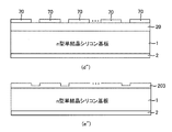
図1は、この発明の実施の形態1による光電変換素子の構成を示す断面図である。図1を参照して、この発明の実施の形態1による光電変換素子100は、n型単結晶シリコン基板1と、パッシベーション膜2と、i型非晶質膜3と、p型非晶質膜11〜1m(mは2以上の整数)と、n型非晶質膜21〜2m−1と、電極31〜3m,41〜4m−1とを備える。
[Embodiment 1]
1 is a cross-sectional view showing a configuration of a photoelectric conversion element according to
n型単結晶シリコン基板1は、例えば、(100)の面方位および0.1〜1.0Ω・cmの比抵抗を有する。また、n型単結晶シリコン基板1は、例えば、100〜300μmの厚みを有し、好ましくは、100〜200μmの厚みを有する。
The n-type single
パッシベーション膜2は、例えば、二酸化シリコン(SiO2)からなり、n型単結晶シリコン基板1の光入射側の表面に接して設けられる。そして、パッシベーション膜2は、例えば、100nmの膜厚を有する。
The
i型非晶質膜3は、非晶質相からなり、n型単結晶シリコン基板1の光入射側の面と反対側の表面に接して設けられる。そして、i型非晶質膜3は、例えば、i型a−Siからなる。また、i型非晶質膜3の膜厚は、p型非晶質膜11〜1mに接する部分およびn型非晶質膜21〜2m−1に接する部分において5〜10nmであり、p型非晶質膜11〜1mおよびn型非晶質膜21〜2m−1に接しない部分において10〜20nmである。
The i-type
p型非晶質膜11〜1mの各々は、非晶質相からなり、i型非晶質膜3に接して設けられる。そして、p型非晶質膜11〜1mの各々は、例えば、p型a−Siからなり、膜厚は、例えば、10nmである。また、p型非晶質膜11〜1mは、n型単結晶シリコン基板1の面内方向において所望の間隔で配置される。更に、p型非晶質膜11〜1mの各々におけるボロン(B)濃度は、例えば、5×1019cm−3である。
Each of the p-type
n型非晶質膜21〜2m−1は、非晶質相からなり、それぞれ、p型非晶質膜11,12間、p型非晶質膜12,13間、・・・、およびp型非晶質膜1m−1,1m間において、i型非晶質膜3に接して配置される。そして、n型非晶質膜21〜2m−1の各々は、例えば、n型a−Siからなり、膜厚は、例えば、10nmである。また、n型非晶質膜21〜2m−1の各々におけるリン(P)濃度は、例えば、5×1019cm−3である。
The n-type
電極31〜3mは、それぞれ、p型非晶質膜11〜1mに接して設けられる。電極41〜4m−1は、それぞれ、n型非晶質膜21〜2m−1に接して設けられる。そして、電極31〜3m,41〜4m−1の各々は、例えば、銀(Ag)からなる。
The
p型非晶質膜11〜1mおよびn型非晶質膜21〜2m−1は、図1の紙面に垂直な方向において同じ長さを有する。そして、p型非晶質膜11〜1mの全体の面積がn型単結晶シリコン基板1の面積に占める割合である面積占有率は、60〜93%であり、n型非晶質膜21〜2m−1の全体の面積がn型単結晶シリコン基板1の面積に占める割合である面積占有率は、5〜20%である。
The p-type amorphous films 11-1m and the n-type amorphous films 21-2m-1 have the same length in the direction perpendicular to the paper surface of FIG. The area occupation ratio, which is the ratio of the entire area of the p-type
このように、p型非晶質膜11〜1mの面積占有率をn型非晶質膜21〜2m−1の面積占有率よりも大きくするのは、n型単結晶シリコン基板1中で光励起された電子および正孔がpin接合(p型非晶質膜11〜1m/i非晶質膜3/n型単結晶シリコン基板1)によって分離され易くし、光励起された電子および正孔の発電への寄与率を高くするためである。
As described above, the area occupancy of the p-type
図2〜図4は、それぞれ、図1に示す光電変換素子100の製造方法を示す第1〜第3の工程図である。
2-4 is a 1st-3rd process drawing which respectively shows the manufacturing method of the
光電変換素子100の製造方法について説明する。光電変換素子100は、プラズマ装置を主に用いてプラズマCVD法によって製造される。
A method for manufacturing the
プラズマ装置は、仕込室と、反応室CB1〜CB3と、取出室と、整合器と、RF電源とを備える。仕込室、反応室CB1〜CB3および取出室は、直列に配置されている。そして、仕込室と反応室CB1との間、反応室CB1と反応室CB2との間、反応室CB2と反応室CB3との間、および反応室CB3と取出室との間は、仕切バルブで仕切られている。また、仕込室から反応室CB1、反応室CB2、反応室CB3および取出室へ単結晶シリコン基板を順次搬送する搬送機構がプラズマ装置に備えられている。 The plasma apparatus includes a preparation chamber, reaction chambers CB1 to CB3, an extraction chamber, a matching unit, and an RF power source. The charging chamber, the reaction chambers CB1 to CB3, and the take-out chamber are arranged in series. A partition valve is used to partition between the charging chamber and the reaction chamber CB1, between the reaction chamber CB1 and the reaction chamber CB2, between the reaction chamber CB2 and the reaction chamber CB3, and between the reaction chamber CB3 and the take-out chamber. It has been. Further, the plasma apparatus is provided with a transport mechanism for sequentially transporting the single crystal silicon substrate from the preparation chamber to the reaction chamber CB1, the reaction chamber CB2, the reaction chamber CB3, and the take-out chamber.
仕込室は、加熱機構と排気機構とを備える。加熱機構は、単結晶シリコン基板を所定の温度に昇温する。排気機構は、仕込室内のガスを排気し、仕込室の到達圧力を、例えば、1×10⁻⁵Pa以下に設定する。 The charging chamber includes a heating mechanism and an exhaust mechanism. The heating mechanism raises the temperature of the single crystal silicon substrate to a predetermined temperature. The exhaust mechanism exhausts the gas in the preparation chamber, and sets the ultimate pressure in the preparation chamber to, for example, 1 × 10 −5 Pa or less.
反応室CB1〜CB3の各々は、平行平板電極と、加熱機構と、排気機構とを備える。加熱機構は、単結晶シリコン基板を所定の温度に昇温する。排気機構は、反応室CB1〜CB3内のガスを排気し、反応室CB1〜CB3の到達圧力を、例えば、1×10⁻⁵Pa以下に設定する。平行平板電極は、整合器を介してRF電源に接続される。なお、反応室CB1は、i型a−Siを堆積するための反応室であり、反応室CB2は、p型a−Siを堆積するための反応室であり、反応室CB3は、n型a−Siを堆積するための反応室である。 Each of the reaction chambers CB1 to CB3 includes a parallel plate electrode, a heating mechanism, and an exhaust mechanism. The heating mechanism raises the temperature of the single crystal silicon substrate to a predetermined temperature. The exhaust mechanism exhausts the gases in the reaction chambers CB1 to CB3, and sets the ultimate pressure in the reaction chambers CB1 to CB3 to, for example, 1 × 10 −5 Pa or less. The parallel plate electrodes are connected to an RF power source through a matching unit. The reaction chamber CB1 is a reaction chamber for depositing i-type a-Si, the reaction chamber CB2 is a reaction chamber for depositing p-type a-Si, and the reaction chamber CB3 is an n-type a-a. A reaction chamber for depositing Si.
取出室は、排気機構を備える。排気機構は、取出室内のガスを排気し、取出室の到達圧力を、例えば、1×10⁻⁵Pa以下に設定する。 The take-out chamber includes an exhaust mechanism. The exhaust mechanism exhausts the gas in the extraction chamber and sets the ultimate pressure in the extraction chamber to, for example, 1 × 10 −5 Pa or less.
仕込室、反応室CB1〜CB3および取出室の各排気機構は、ターボ分子ポンプ、メカニカルブースタポンプおよびロータリーポンプからなる。ターボ分子ポンプ、メカニカルブースタポンプおよびロータリーポンプは、ターボ分子ポンプが仕込室、反応室CB1〜CB3および取出室に最も近くなるように、それぞれ、仕込室、反応室CB1〜CB3および取出室に直列的に連結されている。そして、各排気機構は、ターボ分子ポンプ、メカニカルブースタポンプおよびロータリーポンプによって、それぞれ、仕込室、反応室CB1〜CB3および取出室内のガスを排気し、またはメカニカルブースタポンプおよびロータリーポンプによって、それぞれ、仕込室、反応室CB1〜CB3および取出室内のガスを排気する。 Each exhaust mechanism of the charging chamber, the reaction chambers CB1 to CB3, and the take-out chamber includes a turbo molecular pump, a mechanical booster pump, and a rotary pump. The turbo molecular pump, the mechanical booster pump and the rotary pump are serially connected to the charging chamber, the reaction chambers CB1 to CB3 and the extraction chamber, respectively, so that the turbo molecular pump is closest to the charging chamber, the reaction chambers CB1 to CB3 and the extraction chamber. It is connected to. Each exhaust mechanism exhausts the gas in the charging chamber, reaction chambers CB1 to CB3, and the extraction chamber with a turbo molecular pump, a mechanical booster pump, and a rotary pump, respectively, or is charged with a mechanical booster pump and a rotary pump, respectively. The gases in the chamber, reaction chambers CB1 to CB3 and the extraction chamber are exhausted.
RF電源は、例えば、13.56MHzのRF電力を整合器を介して反応室CB1〜CB3の平行平板電極に印加する。 The RF power source applies, for example, RF power of 13.56 MHz to the parallel plate electrodes of the reaction chambers CB1 to CB3 via the matching unit.
光電変換素子100の製造が開始されると、n型単結晶シリコン基板1をエタノール等で超音波洗浄して脱脂し、その後、n型単結晶シリコン基板1をフッ酸中に浸漬してn型単結晶シリコン基板1の表面に形成された自然酸化膜を除去するとともに、n型単結晶シリコン基板1の表面を水素で終端する(図2の工程(a)参照)。
When the manufacture of the
n型単結晶シリコン基板1の洗浄が終了すると、n型単結晶シリコン基板1を酸化炉に入れ、1000℃の温度で酸素雰囲気中でn型単結晶シリコン基板1を熱酸化する。この場合、酸化時間は、例えば、30分である。そして、n型単結晶シリコン基板1の片側の表面および端面に形成されたSiO2をフッ酸によって除去し、n型単結晶シリコン基板1の一方の表面にSiO2からなるパッシベーション膜2を形成する(図2の工程(b)参照)。
When the cleaning of the n-type single
そして、n型単結晶シリコン基板1/パッシベーション膜2をプラズマ装置の仕込室の基板ホルダー上に配置する。
Then, the n-type single
そして、仕込室の排気機構は、1×10⁻⁵Pa以下に仕込室内のガスを排気し、仕込室の加熱機構は、n型単結晶シリコン基板1/パッシベーション膜2の温度を200℃に設定するように基板ホルダーを加熱する。
And the exhaust mechanism of the preparation chamber exhausts the gas in the preparation chamber to 1 × 10 −5 Pa or less, and the heating mechanism of the preparation chamber sets the temperature of the n-type single
n型単結晶シリコン基板1/パッシベーション膜2の温度が200℃に達すると、仕込室と反応室CB1との間の仕切バルブが開けられ、n型単結晶シリコン基板1/パッシベーション膜2は、仕込室から反応室CB1へ搬送される。
When the temperature of the n-type single
i型非晶質膜3、p型非晶質膜11〜1mおよびn型非晶質膜21〜2m−1を形成するときの材料ガスの流量を表1に示す。
Table 1 shows the flow rates of the material gases when forming the i-type

n型単結晶シリコン基板1/パッシベーション膜2が反応室CB1へ搬送されると、10sccmのシラン(SiH4)ガスと、100sccmの水素(H2)ガスとを反応室CB1に流し、反応室CB1の圧力を13.3Pa〜665Paの範囲に設定する。そして、RF電源は、16〜80mW/cm2の範囲のRFパワーを整合器を介して平行平板電極に印加する。これによって、反応室CB1内でプラズマが発生し、i型a−Siからなるi型非晶質膜20がn型単結晶シリコン基板1の表面(=パッシベーション膜2が形成された面と反対側の表面)に堆積される(図2の工程(c)参照)。
When the n-type single
i型非晶質膜20の膜厚が10〜20nmになると、反応室CB1の平行平板電極へのRFパワーの印加を停止するとともに、SiH4ガスおよびH2ガスの反応室CB1への供給を停止し、排気機構によって1×10⁻⁵Pa以下に反応室CB1を真空引きする。そして、仕切バルブを開け、i型非晶質膜20/n型単結晶シリコン基板1/パッシベーション膜2を反応室CB1から取出室へ搬送し、i型非晶質膜20/n型単結晶シリコン基板1/パッシベーション膜2を室温まで冷却した後、取り出す。
When the film thickness of the i-type
そして、取り出したi型非晶質膜20/n型単結晶シリコン基板1/パッシベーション膜2のi型非晶質膜20の全面にレジストを塗布し、その塗布したレジストをフォトリソグラフィによってパターンニングしてレジストパターン30を形成する(図2の工程(d)参照)。
Then, a resist is applied to the entire surface of the i-type
その後、レジストパターン30をマスクとしてi型非晶質膜20をドライエッチングまたはウェットエッチングによってエッチングし、i型非晶質膜3を形成する(図2の工程(e)参照)。
Thereafter, the i-type
i型非晶質膜3を形成すると、i型非晶質膜3の全面にレジストを塗布し、その塗布したレジストをフォトグラフィによってパターンニングし、レジストパターン40を形成する(図3の工程(f)参照)。
When the i-type
そして、レジストパターン40/i型非晶質膜3/n型単結晶シリコン基板1/パッシベーション膜2のi型非晶質膜3をフッ酸で洗浄し、レジストパターン40/i型非晶質膜3/n型単結晶シリコン基板1/パッシベーション膜2をプラズマ装置の仕込室の基板ホルダー上に配置する。
Then, the resist
そして、仕込室の排気機構は、1×10⁻⁵Pa以下に仕込室内のガスを排気し、仕込室の加熱機構は、レジストパターン40/i型非晶質膜3/n型単結晶シリコン基板1/パッシベーション膜2の温度を200℃に設定するように基板ホルダーを加熱する。
And the exhaust mechanism of the preparation chamber exhausts the gas in the preparation chamber to 1 × 10 −5 Pa or less, and the heating mechanism of the preparation chamber is the resist
レジストパターン40/i型非晶質膜3/n型単結晶シリコン基板1/パッシベーション膜2の温度が200℃に達すると、レジストパターン40/i型非晶質膜3/n型単結晶シリコン基板1/パッシベーション膜2を仕込室から反応室CB2へ搬送する。
When the temperature of resist
レジストパターン40/i型非晶質膜3/n型単結晶シリコン基板1/パッシベーション膜2が反応室CB2へ搬送されると、2sccmのSiH4ガスと、42sccmのH2ガスと、水素希釈された12sccmのジボラン(B2H6)ガスとを反応室CB2に流し(表1参照)、反応室CB2の圧力を13.3Pa〜665Paの範囲に設定する。そして、RF電源は、16〜80mW/cm2の範囲のRFパワーを整合器を介して平行平板電極に印加する。なお、水素希釈されたB2H6ガスの濃度は、0.1%である。これによって、反応室CB2内でプラズマが発生し、p型a−Siからなるp型非晶質膜11〜1mがi型非晶質膜3およびレジストパターン40の表面に堆積される。
When resist
p型非晶質膜11〜1mの膜厚が10nmになると、反応室CB2の平行平板電極へのRFパワーの印加を停止するとともに、SiH4ガス、H2ガスおよびB2H6ガスの反応室CB2への供給を停止し、排気機構によって1×10⁻⁵Pa以下に反応室CB2を真空引きする。そして、仕切バルブを開け、p型非晶質膜11〜1m/レジストパターン40/i型非晶質膜3/n型単結晶シリコン基板1/パッシベーション膜2を反応室CB2から取出室へ搬送する。そして、p型非晶質膜11〜1m/レジストパターン40/i型非晶質膜3/n型単結晶シリコン基板1/パッシベーション膜2を室温まで冷却し、取出室から取出す。
When the thickness of the p-type
その後、p型非晶質膜11〜1m/レジストパターン40/i型非晶質膜3/n型単結晶シリコン基板1/パッシベーション膜2のレジストパターン40を除去する。これによって、レジストパターン40上に堆積されたp型a−Siは、リフトオフによって除去され、p型非晶質膜11〜1mがi型非晶質膜3の薄膜部に接して形成された構造が作製される(図3の工程(g)参照)。
Thereafter, the resist
引き続いて、p型非晶質膜11〜1m/i型非晶質膜3/n型単結晶シリコン基板1/パッシベーション膜2のp型非晶質膜11〜1mおよびi型非晶質膜3上にレジストを塗布し、その塗布したレジストをフォトリソグラフィによってパターンニングしてレジストパターン50を形成する(図3の工程(h)参照)。
Subsequently, the p-type
その後、レジストパターン50/p型非晶質膜11〜1m/i型非晶質膜3/n型単結晶シリコン基板1/パッシベーション膜2のi型非晶質膜3をフッ酸で洗浄し、レジストパターン50/p型非晶質膜11〜1m/i型非晶質膜3/n型単結晶シリコン基板1/パッシベーション膜2をプラズマ装置の仕込室の基板ホルダー上に配置する。
Thereafter, the resist
その後、仕込室の排気機構は、1×10⁻⁵Pa以下に仕込室内のガスを排気し、仕込室の加熱機構は、レジストパターン50/p型非晶質膜11〜1m/i型非晶質膜3/n型単結晶シリコン基板1/パッシベーション膜2の温度を200℃に設定するように基板ホルダーを加熱する。
Thereafter, the exhaust mechanism in the preparation chamber exhausts the gas in the preparation chamber to 1 × 10 −5 Pa or less, and the heating mechanism in the preparation chamber is a resist
レジストパターン50/p型非晶質膜11〜1m/i型非晶質膜3/n型単結晶シリコン基板1/パッシベーション膜2の温度が200℃に達すると、レジストパターン50/p型非晶質膜11〜1m/i型非晶質膜3/n型単結晶シリコン基板1/パッシベーション膜2を仕込室から反応室CB3へ搬送する。
When the temperature of the resist
レジストパターン50/p型非晶質膜11〜1m/i型非晶質膜3/n型単結晶シリコン基板1/パッシベーション膜2が反応室CB3へ搬送されると、20sccmのSiH4ガスと、150sccmのH2ガスと、水素希釈された50sccmのフォスフィン(PH3)ガスとを反応室CB3に流し(表1参照)、反応室CB3の圧力を13.3Pa〜665Paの範囲に設定する。そして、RF電源は、16〜80mW/cm2の範囲のRFパワーを整合器を介して平行平板電極に印加する。なお、水素希釈されたPH3ガスの濃度は、0.2%である。これによって、反応室CB3内でプラズマが発生し、n型a−Siからなるn型非晶質膜21〜2m−1がi型非晶質膜3およびレジストパターン50の表面に堆積される。
When the resist
n型非晶質膜21〜2m−1の膜厚が10nmになると、反応室CB3の平行平板電極へのRFパワーの印加を停止するとともに、SiH4ガス、H2ガスおよびPH3ガスの反応室CB3への供給を停止し、排気機構によって1×10⁻⁵Pa以下に反応室CB3を真空引きする。そして、仕切バルブを開け、n型非晶質膜21〜2m−1/レジストパターン50/p型非晶質膜11〜1m/i型非晶質膜3/n型単結晶シリコン基板1/パッシベーション膜2を反応室CB3から取出室へ搬送する。そして、n型非晶質膜21〜2m−1/レジストパターン50/p型非晶質膜11〜1m/i型非晶質膜3/n型単結晶シリコン基板1/パッシベーション膜2を室温まで冷却し、取出室から取出す。
When the thickness of the n-type
その後、n型非晶質膜21〜2m−1/レジストパターン50/p型非晶質膜11〜1m/i型非晶質膜3/n型単結晶シリコン基板1/パッシベーション膜2のレジストパターン50を除去する。これによって、レジストパターン50上に堆積されたn型a−Siは、リフトオフによって除去され、n型非晶質膜21〜2m−1がi型非晶質膜3の薄膜部に接して形成された構造が作製される(図3の工程(i)参照)。
Thereafter, the resist pattern of n-type amorphous film 21-2m-1 / resist
引き続いて、n型非晶質膜21〜2m−1およびp型非晶質膜11〜1m側にAgを蒸着し、その蒸着したAgをフォトリソグラフィおよびエッチングによってパターンニングし、電極31〜3m,41〜4m−1を形成する。これによって、光電変換素子100が完成する(図4の工程(j)参照)。
Subsequently, Ag is vapor-deposited on the n-type
光電変換素子100において、太陽光がパッシベーション膜2側から光電変換素子100に照射されると、n型単結晶シリコン基板1中で電子および正孔が光励起される。
In the
光励起された電子および正孔は、パッシベーション膜2側へ拡散しても、パッシベーション膜2によるn型単結晶シリコン基板1のパッシベーション効果によって再結合し難く、p型非晶質膜11〜1mおよびn型非晶質膜21〜2m−1側へ拡散する。
Even if the photoexcited electrons and holes are diffused to the
そして、p型非晶質膜11〜1mおよびn型非晶質膜21〜2m−1側へ拡散した電子および正孔は、p型非晶質膜11〜1m/i型非晶質膜3/n型単結晶シリコン基板1(=pin接合)による内部電界によって分離され、正孔は、i型非晶質膜3およびp型非晶質膜11〜1mを介して電極31〜3mへ到達し、電子は、i型非晶質膜3およびn型非晶質膜21〜2m−1を介して電極41〜4m−1へ到達する。
Then, the electrons and holes diffused toward the p-type
電極41〜4m−1へ到達した電子は、電極31〜3mと電極41〜4m−1との間に接続された負荷を介して電極31〜3mへ到達し、正孔と再結合する。
The electrons that have reached the
このように、光電変換素子100は、n型単結晶シリコン基板1中で光励起された電子および正孔をn型単結晶シリコン基板1の裏面(=パッシベーション膜2が形成されたn型単結晶シリコン基板1の表面と反対側の面)から取り出すバックコンタクト型の光電変換素子である。
As described above, the
そして、光電変換素子100においては、i型非晶質膜3において、p型非晶質膜11〜1mおよびn型非晶質膜21〜2m−1に接する部分の膜厚(=5〜10nm)がp型非晶質膜11〜1mおよびn型非晶質膜21〜2m−1に接しない部分の膜厚(=10〜20nm)よりも薄い。その結果、正孔がn型単結晶シリコン基板1からi型非晶質膜3およびp型非晶質膜11〜1mを介して電極31〜3mへ到達するときの直列抵抗が低下するとともに、電子がn型単結晶シリコン基板1からi型非晶質膜3およびn型非晶質膜21〜2m−1を介して電極41〜4m−1へ到達するときの直列抵抗が低下する。また、p型非晶質膜11〜1mおよびn型非晶質膜21〜2m−1に接しないi型非晶質膜3の部分は、20nm程度の膜厚があるので、n型単結晶シリコン基板1の裏面に対するパッシベーション効果が高く、n型単結晶シリコン基板1の裏面におけるキャリア(電子および正孔)の再結合が抑制される。
In the
従って、光電変換素子100の曲線因子FFおよび開放電圧Vocを向上できる。
Therefore, the fill factor FF and the open circuit voltage Voc of the
上記においては、i型非晶質膜3は、i型a−Siからなると説明したが、実施の形態1においては、これに限らず、i型非晶質膜3は、i型a−SiC、i型a−SiO、i型a−SiN、i型a−SiCNおよびi型a−SiGeのいずれかからなっていてもよい。
In the above description, the i-type
また、p型非晶質膜11〜1mの各々は、p型a−Siからなると説明したが、実施の形態1においては、これに限らず、p型非晶質膜11〜1mの各々は、p型a−SiC、p型a−SiO、p型a−SiN、p型a−SiCN、p型a−SiGeおよびp型a−Geのいずれかからなっていてもよい。
In addition, it has been described that each of the p-type
更に、n型非晶質膜21〜2m−1の各々は、n型a−Siからなると説明したが、実施の形態1においては、これに限らず、n型非晶質膜21〜2m−1の各々は、n型a−SiC、n型a−SiO、n型a−SiN、n型a−SiCN、n型a−SiGeおよびn型a−Geのいずれかからなっていてもよい。
Further, it has been described that each of the n-type
即ち、光電変換素子100においては、p型非晶質膜11〜1m、n型非晶質膜21〜2m−1およびi型非晶質膜3は、それぞれ、表2に示す材料のいずれかからなっていてもよい。
That is, in the
この場合、p型a−SiCは、SiH4ガス、メタン(CH4)ガス、B2H6ガスおよびH2ガスを材料ガスとして、上述したプラズマCVD法によって形成される。p型a−SiOは、SiH4ガス、酸素(O2)ガス、B2H6ガスおよびH2ガスを材料ガスとして、上述したプラズマCVD法によって形成される。p型a−SiNは、SiH4ガス、アンモニア(NH3)ガス、B2H6ガスおよびH2ガスを材料ガスとして、上述したプラズマCVD法によって形成される。p型a−SiCNは、SiH4ガス、CH4ガス、NH3ガス、B2H6ガスおよびH2ガスを材料ガスとして、上述したプラズマCVD法によって形成される。p型a−SiGeは、SiH4ガス、ゲルマン(GeH4)ガス、B2H6ガスおよびH2ガスを材料ガスとして、上述したプラズマCVD法によって形成される。p型a−Geは、GeH4ガス、B2H6ガスおよびH2ガスを材料ガスとして、上述したプラズマCVD法によって形成される。 In this case, the p-type a-SiC is formed by the above-described plasma CVD method using SiH 4 gas, methane (CH 4 ) gas, B 2 H 6 gas, and H 2 gas as material gases. The p-type a-SiO is formed by the above-described plasma CVD method using SiH 4 gas, oxygen (O 2 ) gas, B 2 H 6 gas and H 2 gas as material gases. The p-type a-SiN is formed by the above-described plasma CVD method using SiH 4 gas, ammonia (NH 3 ) gas, B 2 H 6 gas and H 2 gas as material gases. The p-type a-SiCN is formed by the above-described plasma CVD method using SiH 4 gas, CH 4 gas, NH 3 gas, B 2 H 6 gas and H 2 gas as material gases. The p-type a-SiGe is formed by the above-described plasma CVD method using SiH 4 gas, germane (GeH 4 ) gas, B 2 H 6 gas and H 2 gas as material gases. The p-type a-Ge is formed by the above-described plasma CVD method using GeH 4 gas, B 2 H 6 gas, and H 2 gas as material gases.
また、n型a−SiCは、SiH4ガス、CH4ガス、PH3ガスおよびH2ガスを材料ガスとして、上述したプラズマCVD法によって形成される。n型a−SiOは、SiH4ガス、O2ガス、PH3ガスおよびH2ガスを材料ガスとして、上述したプラズマCVD法によって形成される。n型a−SiNは、SiH4ガス、NH3ガス、PH3ガスおよびH2ガスを材料ガスとして、上述したプラズマCVD法によって形成される。n型a−SiCNは、SiH4ガス、CH4ガス、NH3ガス、PH3ガスおよびH2ガスを材料ガスとして、上述したプラズマCVD法によって形成される。n型a−SiGeは、SiH4ガス、GeH4ガス、PH3ガスおよびH2ガスを材料ガスとして、上述したプラズマCVD法によって形成される。n型a−Geは、GeH4ガス、PH3ガスおよびH2ガスを材料ガスとして、上述したプラズマCVD法によって形成される。 The n-type a-SiC is formed by the above-described plasma CVD method using SiH 4 gas, CH 4 gas, PH 3 gas, and H 2 gas as material gases. The n-type a-SiO is formed by the above-described plasma CVD method using SiH 4 gas, O 2 gas, PH 3 gas, and H 2 gas as material gases. The n-type a-SiN is formed by the above-described plasma CVD method using SiH 4 gas, NH 3 gas, PH 3 gas, and H 2 gas as material gases. The n-type a-SiCN is formed by the above-described plasma CVD method using SiH 4 gas, CH 4 gas, NH 3 gas, PH 3 gas, and H 2 gas as material gases. The n-type a-SiGe is formed by the above-described plasma CVD method using SiH 4 gas, GeH 4 gas, PH 3 gas, and H 2 gas as material gases. The n-type a-Ge is formed by the above-described plasma CVD method using GeH 4 gas, PH 3 gas, and H 2 gas as material gases.
更に、i型a−SiCは、SiH4ガス、CH4ガスおよびH2ガスを材料ガスとして、上述したプラズマCVD法によって形成される。i型a−SiOは、SiH4ガス、O2ガスおよびH2ガスを材料ガスとして、上述したプラズマCVD法によって形成される。i型a−SiNは、SiH4ガス、NH3ガスおよびH2ガスを材料ガスとして、上述したプラズマCVD法によって形成される。i型a−SiCNは、SiH4ガス、CH4ガス、NH3ガスおよびH2ガスを材料ガスとして、上述したプラズマCVD法によって形成される。i型a−SiGeは、SiH4ガス、GeH4ガスおよびH2ガスを材料ガスとして、上述したプラズマCVD法によって形成される。 Furthermore, i-type a-SiC is formed by the above-described plasma CVD method using SiH 4 gas, CH 4 gas, and H 2 gas as material gases. i-type a-SiO is formed by the above-described plasma CVD method using SiH 4 gas, O 2 gas, and H 2 gas as material gases. i-type a-SiN is formed by the above-described plasma CVD method using SiH 4 gas, NH 3 gas, and H 2 gas as material gases. The i-type a-SiCN is formed by the above-described plasma CVD method using SiH 4 gas, CH 4 gas, NH 3 gas, and H 2 gas as material gases. i-type a-SiGe is formed by the above-described plasma CVD method using SiH 4 gas, GeH 4 gas, and H 2 gas as material gases.
なお、i型非晶質膜3としては、i型a−Geも想定されるが、i型a−Geは、n型単結晶シリコン基板1よりも光学バンドギャップが小さいので、i型a−Geをi型非晶質膜3として用いた場合、開放電圧Vocの向上が困難である。光電変換素子100においては、i型非晶質膜3の光学バンドギャップが開放電圧Vocを支配的に決定するからである。
Note that i-type a-Ge is also assumed as the i-type
そこで、実施の形態1においては、n型単結晶シリコン基板1の光学バンドギャップよりも大きい光学バンドギャップを有するi型a−SiC,i型a−SiO,i型a−SiN,i型a−SiCN,i型a−Si,i型a−SiGeをi型非晶質膜3として用いることにした。
Therefore, in the first embodiment, i-type a-SiC, i-type a-SiO, i-type a-SiN, and i-type a- having an optical band gap larger than the optical band gap of the n-type single
また、光電変換素子100においては、p型非晶質膜11〜1mに接するi型非晶質膜3の膜厚は、n型非晶質膜21〜2m−1に接するi型非晶質膜3の膜厚と同じであってもよく、異なっていてもよい。
In the
更に、光電変換素子100においては、電極31〜3mの幅は、それぞれ、p型非晶質膜11〜1mの幅以上であればよく、電極41〜4m−1の幅は、それぞれ、n型非晶質膜21〜2m−1の幅以上であればよい。
Furthermore, in the
更に、光電変換素子100においては、n型単結シリコン基板1のパッシベーション膜2側の表面は、テクスチャ化されていてもよい。
Furthermore, in the
[実施の形態2]
図5は、実施の形態2による光電変換素子の構成を示す断面図である。図5を参照して、実施の形態2による光電変換素子200は、図1に示す光電変換素子100のi型非晶質膜3をi型非晶質膜103に代えたものであり、その他は、光電変換素子100と同じである。
[Embodiment 2]
FIG. 5 is a cross-sectional view showing the configuration of the photoelectric conversion element according to the second embodiment. Referring to FIG. 5, a
i型非晶質膜103は、非晶質相からなり、n型単結晶シリコン基板1の光入射側の面と反対側の表面に接して設けられる。そして、i型非晶質膜103は、例えば、i型a−Siからなる。また、i型非晶質膜103の膜厚は、p型非晶質膜11〜1mに接する部分において5〜10nmであり、n型非晶質膜21〜2m−1に接する部分と、p型非晶質膜11〜1mおよびn型非晶質膜21〜2m−1に接しない部分とにおいて10〜20nmである。
The i-type
このように、光電変換素子200においては、p型非晶質膜11〜1mは、i型非晶質膜103の薄膜部に接して配置され、n型非晶質膜21〜2m−1は、i型非晶質膜103の厚膜部に接して配置される。
As described above, in the
図6は、図5に示す光電変換素子200の製造工程の一部を示す工程図である。光電変換素子200は、図2から図4に示す工程(a)〜工程(l)の工程(d),(e)をそれぞれ図6に示す工程(d’),(e’)に代えた工程に従って製造される。
FIG. 6 is a process diagram showing a part of the manufacturing process of the
光電変換素子200の製造が開始されると、上述した工程(a)〜工程(c)が順次実行される。そして、工程(c)の後、i型非晶質膜20上にレジストを塗布し、その塗布したレジストをフォトリソグラフィによってパターンニングし、レジストパターン60を形成する(図6の工程(d’)参照)。
When the manufacture of the
その後、レジストパターン60をマスクとしてi型非晶質膜20をドライエッチングまたはウェットエッチングによってエッチングし、i型非晶質膜103を形成する(図8の工程(e’)参照)。
Thereafter, the i-type
そして、上述した工程(f)〜(j)が順次実行され、光電変換素子200が完成する。
And the process (f)-(j) mentioned above is performed sequentially, and the
光電変換素子200において、太陽光がパッシベーション膜2側から光電変換素子200に照射されると、n型単結晶シリコン基板1中で電子および正孔が光励起される。
In the
光励起された電子および正孔は、パッシベーション膜2側へ拡散しても、パッシベーション膜2によるn型単結晶シリコン基板1のパッシベーション効果によって再結合し難く、p型非晶質膜11〜1mおよびn型非晶質膜21〜2m−1側へ拡散する。
Even if the photoexcited electrons and holes are diffused to the
そして、p型非晶質膜11〜1mおよびn型非晶質膜21〜2m−1側へ拡散した電子および正孔は、p型非晶質膜11〜1m/i型非晶質膜103/n型単結晶シリコン基板1(=pin接合)による内部電界によって分離され、正孔は、i型非晶質膜103およびp型非晶質膜11〜1mを介して電極31〜3mへ到達し、電子は、i型非晶質膜103およびn型非晶質膜21〜2m−1を介して電極41〜4m−1へ到達する。
The electrons and holes diffused toward the p-type
電極41〜4m−1へ到達した電子は、電極31〜3mと電極41〜4m−1との間に接続された負荷を介して電極31〜3mへ到達し、正孔と再結合する。
The electrons that have reached the
このように、光電変換素子200は、n型単結晶シリコン基板1中で光励起された電子および正孔をn型単結晶シリコン基板1の裏面(=パッシベーション膜2が形成されたn型単結晶シリコン基板1の表面と反対側の面)から取り出すバックコンタクト型の光電変換素子である。
As described above, the
そして、光電変換素子200においては、i型非晶質膜103の膜厚は、p型非晶質膜11〜1mに接する部分において5〜10nmであり、n型非晶質膜21〜2m−1に接する部分と、p型非晶質膜11〜1mおよびn型非晶質膜21〜2m−1に接しない部分とにおいて10〜20nmである。
In the
その結果、正孔がn型単結晶シリコン基板1からi型非晶質膜103およびp型非晶質膜11〜1mを介して電極31〜3mへ到達するときの直列抵抗が低下する。また、n型非晶質膜21〜2m−1に接する部分と、p型非晶質膜11〜1mおよびn型非晶質膜21〜2m−1に接しない部分とは、20nm程度の膜厚を有するので、n型単結晶シリコン基板1の裏面に対するパッシベーション効果が高く、n型単結晶シリコン基板1の裏面におけるキャリア(電子および正孔)の再結合が抑制される。
As a result, the series resistance when holes reach the
従って、光電変換素子200の曲線因子FFおよび開放電圧Vocを向上できる。
Therefore, the fill factor FF and the open circuit voltage Voc of the
上記においては、i型非晶質膜103は、i型a−Siからなると説明したが、実施の形態2においては、これに限らず、i型非晶質膜103は、i型a−SiC、i型a−SiO、i型a−SiN、i型a−SiCNおよびi型a−SiGeのいずれかからなっていてもよい。即ち、i型非晶質膜103は、表2に示すi型非晶質膜3を構成する材料のいずれかからなっていてもよい。そして、i型非晶質膜103を構成する材料としてi型a−Geが除外されるのは、i型非晶質膜3を構成する材料としてi型a−Geが除外される理由(実施の形態1参照)と同じである。
In the above description, the i-type
実施の形態2におけるその他の説明は、実施の形態1における説明と同じである。 Other explanations in the second embodiment are the same as those in the first embodiment.
[実施の形態3]
図7は、実施の形態3による光電変換素子の構成を示す断面図である。図7を参照して、実施の形態3による光電変換素子300は、図1に示す光電変換素子100のi型非晶質膜3をi型非晶質膜203に代えたものであり、その他は、光電変換素子100と同じである。
[Embodiment 3]
FIG. 7 is a cross-sectional view showing the configuration of the photoelectric conversion element according to the third embodiment. 7,
i型非晶質膜203は、非晶質相からなり、n型単結晶シリコン基板1の光入射側の面と反対側の表面に接して設けられる。そして、i型非晶質膜203は、例えば、i型a−Siからなる。また、i型非晶質膜203の膜厚は、n型非晶質膜21〜2m−1に接する部分において5〜10nmであり、p型非晶質膜11〜1mに接する部分と、p型非晶質膜11〜1mおよびn型非晶質膜21〜2m−1に接しない部分とにおいて10〜20nmである。
The i-type
このように、光電変換素子300においては、n型非晶質膜21〜2m−1は、i型非晶質膜203の薄膜部に接して配置され、p型非晶質膜11〜1mは、i型非晶質膜203の厚膜部に接して配置される。
Thus, in the
図8は、図7に示す光電変換素子300の製造工程の一部を示す工程図である。光電変換素子300は、図2から図4に示す工程(a)〜工程(l)の工程(d),(e)をそれぞれ図8に示す工程(d”),(e”)に代えた工程に従って製造される。
FIG. 8 is a process diagram showing a part of the manufacturing process of the
光電変換素子300の製造が開始されると、上述した工程(a)〜工程(c)が順次実行される。そして、工程(c)の後、i型非晶質膜20上にレジストを塗布し、その塗布したレジストをフォトリソグラフィによってパターンニングし、レジストパターン70を形成する(図8の工程(d”)参照)。
When the manufacture of the
その後、レジストパターン70をマスクとしてi型非晶質膜20をドライエッチングまたはウェットエッチングによってエッチングし、i型非晶質膜203を形成する(図8の工程(e”)参照)。
Thereafter, using the resist
そして、上述した工程(f)〜(j)が順次実行され、光電変換素子300が完成する。
And the process (f)-(j) mentioned above is performed sequentially, and the
光電変換素子300において、太陽光がパッシベーション膜2側から光電変換素子300に照射されると、n型単結晶シリコン基板1中で電子および正孔が光励起される。
In the
光励起された電子および正孔は、パッシベーション膜2側へ拡散しても、パッシベーション膜2によるn型単結晶シリコン基板1のパッシベーション効果によって再結合し難く、非晶質膜11〜1m,21〜2m−1側へ拡散する。
Even if the photoexcited electrons and holes diffuse to the
そして、非晶質膜11〜1m,21〜2m−1側へ拡散した電子および正孔は、p型非晶質膜11〜1m/i型非晶質膜203/n型単結晶シリコン基板1(=pin接合)による内部電界によって分離され、正孔は、i型非晶質膜203およびp型非晶質膜11〜1mを介して電極31〜3mへ到達し、電子は、i型非晶質膜203およびn型非晶質膜21〜12m−1を介して電極41〜4m−1へ到達する。
Then, the electrons and holes diffused toward the
電極41〜4m−1へ到達した電子は、電極31〜3mと電極41〜4m−1との間に接続された負荷を介して電極31〜3mへ到達し、正孔と再結合する。
The electrons that have reached the
このように、光電変換素子300は、n型単結晶シリコン基板1中で光励起された電子および正孔をn型単結晶シリコン基板1の裏面(=パッシベーション膜2が形成されたn型単結晶シリコン基板1の表面と反対側の面)から取り出すバックコンタクト型の光電変換素子である。
As described above, the
そして、光電変換素子300においては、i型非晶質膜203の膜厚は、n型非晶質膜21〜2m−1に接する部分において5〜10nmであり、p型非晶質膜11〜1mに接する部分と、p型非晶質膜11〜1mおよびn型非晶質膜21〜2m−1に接しない部分とにおいて10〜20nmである。
In the
その結果、電子がn型単結晶シリコン基板1からi型非晶質膜203およびn型非晶質膜21〜2m−1を介して電極41〜4m−1へ到達するときの直列抵抗が低下する。また、p型非晶質膜11〜1mに接する部分と、p型非晶質膜11〜1mおよびn型非晶質膜21〜2m−1に接しない部分とは、20nm程度の膜厚を有するので、n型単結晶シリコン基板1の裏面に対するパッシベーション効果が高く、n型単結晶シリコン基板1の裏面におけるキャリア(電子および正孔)の再結合が抑制される。
As a result, the series resistance when electrons reach the
従って、光電変換素子300の曲線因子FFおよび開放電圧Vocを向上できる。
Therefore, the fill factor FF and the open circuit voltage Voc of the
上記においては、i型非晶質膜203は、i型a−Siからなると説明したが、実施の形態3においては、これに限らず、i型非晶質膜203は、i型a−SiC、i型a−SiO、i型a−SiN、i型a−SiCNおよびi型a−SiGeのいずれかからなっていてもよい。即ち、i型非晶質膜203は、表2に示すi型非晶質膜3を構成する材料のいずれかからなっていてもよい。そして、i型非晶質膜203を構成する材料としてi型a−Geが除外されるのは、i型非晶質膜3を構成する材料としてi型a−Geが除外される理由(実施の形態1参照)と同じである。
In the above description, the i-type
実施の形態3におけるその他の説明は、実施の形態1における説明と同じである。 Other explanations in the third embodiment are the same as those in the first embodiment.
上記においては、単結晶シリコン基板としてn型単結晶シリコン基板1を備える光電変換素子100,200,300について説明したが、この発明の実施の形態による光電変換素子は、単結晶シリコン基板としてp型単結晶シリコン基板を備える光電変換素子であってもよい。
In the above, the
この場合、p型非晶質膜11〜1mに代えてn型非晶質膜が用いられ、n型非晶質膜21〜2m−1に代えてp型非晶質膜が用いられる。
In this case, an n-type amorphous film is used instead of the p-type
そして、p型単結晶シリコン基板を備える光電変換素子は、上述した工程(a)〜(j)、工程(a)〜(c),(d’),(e’),(f)〜(j)および工程(a)〜(c),(d”),(e”),(f)〜(j)のいずれかに従って製造される。 And a photoelectric conversion element provided with a p-type single crystal silicon substrate has the steps (a) to (j), steps (a) to (c), (d ′), (e ′), (f) to (f) described above. j) and steps (a) to (c), (d ″), (e ″), and (f) to (j).
実施の形態1においては、i型非晶質膜3において、p型非晶質膜11〜1mに接する部分およびn型非晶質膜21〜2m−1に接する部分の膜厚がp型非晶質膜11〜1mおよびn型非晶質膜21〜2m−1に接しない部分の膜厚よりも薄い場合について説明した。
In the first embodiment, in the i-type
また、実施の形態2においては、i型非晶質膜103において、p型非晶質膜11〜1mに接する部分の膜厚がn型非晶質膜21〜2m−1に接する部分の膜厚と、p型非晶質膜11〜1mおよびn型非晶質膜21〜2m−1に接しない部分の膜厚とよりも薄い場合について説明した。
In the second embodiment, in the i-type
更に、実施の形態3においては、i型非晶質膜203において、n型非晶質膜21〜2m−1に接する部分の膜厚がp型非晶質膜11〜1mに接する部分の膜厚と、p型非晶質膜11〜1mおよびn型非晶質膜21〜2m−1に接しない部分の膜厚とよりも薄い場合について説明した。
Further, in the third embodiment, in the i-type
従って、この発明の実施の形態による光電変換素子は、第1の導電型を有する単結晶シリコンからなる半導体基板と、半導体基板の一方の表面に接して設けられ、i型の導電型を有する第1の非晶質膜と、第1の非晶質膜に接して設けられ、第1の導電型と反対の第2の導電型を有する第2の非晶質膜と、半導体基板の面内方向において第2の非晶質膜に隣接し、かつ、第1の非晶質膜に接して設けられ、第1の導電型を有する第3の非晶質膜とを備え、第1の非晶質膜において、第2および第3の非晶質膜の少なくとも一方と接する部分の膜厚が第2および第3の非晶質膜の少なくとも一方と接しない部分の膜厚よりも薄ければよい。 Therefore, the photoelectric conversion element according to the embodiment of the present invention is provided with a semiconductor substrate made of single crystal silicon having the first conductivity type, and in contact with one surface of the semiconductor substrate, and having the i-type conductivity type. A first amorphous film, a second amorphous film provided in contact with the first amorphous film and having a second conductivity type opposite to the first conductivity type, and an in-plane of the semiconductor substrate And a third amorphous film having a first conductivity type and adjacent to the second amorphous film in the direction and in contact with the first amorphous film. In the crystalline film, if the thickness of the portion in contact with at least one of the second and third amorphous films is smaller than the thickness of the portion not in contact with at least one of the second and third amorphous films Good.
そして、n型単結晶シリコン基板1が用いられる場合、第1の導電型は、n型であり、第2の導電型は、p型である。また、p型単結晶シリコン基板が用いられる場合、第1の導電型は、p型であり、第2の導電型は、n型である。
When the n-type single
また、この発明の実施の形態による光電変換素子の製造方法は、上述した光電変換素子100,200,300と、光電変換素子100,200,300と同様の裏面構造を有し、p型単結晶シリコン基板を用いた光電変換素子を製造する製造方法であればよい。従って、この発明の実施の形態による光電変換素子の製造方法は、第1の導電型を有する単結晶シリコンからなる半導体基板の一方の表面に接して、i型の導電型を有する第1の非晶質膜を形成する第1の工程と、半導体基板の面内方向において第1の非晶質膜の一部分を除去する第2の工程と、第1の導電型と反対の第2の導電型を有する第2の非晶質膜を第1の非晶質膜に接して形成する第3の工程と、半導体基板の面内方向において第2の非晶質膜に隣接し、かつ、第1の非晶質膜に接して、第1の導電型を有する第3の非晶質膜を形成する第4の工程とを備え、第3および第4の工程の少なくとも一方において、第2および第3の非晶質膜の少なくとも一方は、一部分が除去された第1の非晶質膜に接して形成されるものであればよい。 Moreover, the manufacturing method of the photoelectric conversion element by this Embodiment has the back surface structure similar to the photoelectric conversion element 100,200,300 mentioned above, and the photoelectric conversion element 100,200,300, and is a p-type single crystal. Any manufacturing method for manufacturing a photoelectric conversion element using a silicon substrate may be used. Therefore, the method for manufacturing the photoelectric conversion element according to the embodiment of the present invention is in contact with one surface of the semiconductor substrate made of single crystal silicon having the first conductivity type, and the first non-conductive type having the i-type conductivity type. A first step of forming a crystalline film; a second step of removing a portion of the first amorphous film in the in-plane direction of the semiconductor substrate; and a second conductivity type opposite to the first conductivity type A third step of forming a second amorphous film in contact with the first amorphous film; adjacent to the second amorphous film in the in-plane direction of the semiconductor substrate; and A fourth step of forming a third amorphous film having the first conductivity type in contact with the amorphous film, and in at least one of the third and fourth steps, the second and second At least one of the three amorphous films may be formed in contact with the first amorphous film from which a part has been removed. .
今回開示された実施の形態はすべての点で例示であって制限的なものではないと考えられるべきである。本発明の範囲は、上記した実施の形態の説明ではなくて特許請求の範囲によって示され、特許請求の範囲と均等の意味および範囲内でのすべての変更が含まれることが意図される。 The embodiment disclosed this time should be considered as illustrative in all points and not restrictive. The scope of the present invention is shown not by the above description of the embodiments but by the scope of claims for patent, and is intended to include meanings equivalent to the scope of claims for patent and all modifications within the scope.
この発明は、光電変換素子およびその製造方法に適用される。 The present invention is applied to a photoelectric conversion element and a manufacturing method thereof.
1 n型単結晶シリコン基板、2 パッシベーション膜、3,20,103,203 i非晶質膜、11〜1m p型非晶質膜、21〜2m−1 n型非晶質膜、30,40,50,60,70 レジストパターン、31〜3m,41〜4m−1 電極、100,200,300 光電変換素子。 1 n-type single crystal silicon substrate, 2 passivation film, 3, 20, 103, 203 i amorphous film, 11-1mp p-type amorphous film, 21-2m-1 n-type amorphous film, 30, 40 , 50, 60, 70 Resist pattern, 31 to 3 m, 41 to 4 m-1 electrode, 100, 200, 300 Photoelectric conversion element.
Claims (13)
前記半導体基板の一方の表面に接して設けられ、i型の導電型を有する第1の非晶質膜と、
前記第1の非晶質膜に接して設けられ、前記第1の導電型と反対の第2の導電型を有する第2の非晶質膜と、
前記半導体基板の面内方向において前記第2の非晶質膜に隣接し、かつ、前記第1の非晶質膜に接して設けられ、前記第1の導電型を有する第3の非晶質膜とを備え、
前記第1の非晶質膜において、前記第2および第3の非晶質膜の少なくとも一方と接する部分の膜厚が前記第2および第3の非晶質膜の少なくとも一方と接しない部分の膜厚よりも薄い、光電変換素子。 A semiconductor substrate made of single crystal silicon having a first conductivity type;
A first amorphous film provided in contact with one surface of the semiconductor substrate and having an i-type conductivity;
A second amorphous film provided in contact with the first amorphous film and having a second conductivity type opposite to the first conductivity type;
A third amorphous material that is provided adjacent to the second amorphous film and in contact with the first amorphous film in the in-plane direction of the semiconductor substrate and has the first conductivity type With a membrane,
In the first amorphous film, the thickness of the portion in contact with at least one of the second and third amorphous films is not in contact with at least one of the second and third amorphous films. A photoelectric conversion element that is thinner than the film thickness.
前記第2の非晶質膜は、p型の導電型を有し、
前記第3の非晶質膜は、n型の導電型を有する、請求項1から請求項5のいずれか1項に記載の光電変換素子。 The semiconductor substrate is made of n-type single crystal silicon,
The second amorphous film has a p-type conductivity type,
The photoelectric conversion element according to claim 1, wherein the third amorphous film has an n-type conductivity type.
前記第3の非晶質膜は、n型アモルファスシリコンカーバイド、n型アモルファスシリコンナイトライド、n型アモルファスシリコンカーボンナイトライド、n型アモルファスシリコンオキサイド、n型アモルファスシリコン、n型アモルファスシリコンゲルマニウムおよびn型アモルファスゲルマニウムのいずれかからなる、請求項6に記載の光電変換素子。 The second amorphous film includes p-type amorphous silicon carbide, p-type amorphous silicon nitride, p-type amorphous silicon carbon nitride, p-type amorphous silicon oxide, p-type amorphous silicon, p-type amorphous silicon germanium, and p-type. Made of either amorphous germanium,
The third amorphous film includes n-type amorphous silicon carbide, n-type amorphous silicon nitride, n-type amorphous silicon carbon nitride, n-type amorphous silicon oxide, n-type amorphous silicon, n-type amorphous silicon germanium, and n-type. The photoelectric conversion element according to claim 6, comprising any of amorphous germanium.
前記第2の非晶質膜は、n型の導電型を有し、
前記第3の非晶質膜は、p型の導電型を有する、請求項1から請求項5のいずれか1項に記載の光電変換素子。 The semiconductor substrate is made of p-type single crystal silicon,
The second amorphous film has an n-type conductivity type,
The photoelectric conversion element according to any one of claims 1 to 5, wherein the third amorphous film has a p-type conductivity type.
前記第3の非晶質膜は、p型アモルファスシリコンカーバイド、p型アモルファスシリコンナイトライド、p型アモルファスシリコンカーボンナイトライド、p型アモルファスシリコンオキサイド、p型アモルファスシリコン、p型アモルファスシリコンゲルマニウムおよびp型アモルファスゲルマニウムのいずれかからなる、請求項8に記載の光電変換素子。 The second amorphous film includes n-type amorphous silicon carbide, n-type amorphous silicon nitride, n-type amorphous silicon carbon nitride, n-type amorphous silicon oxide, n-type amorphous silicon, n-type amorphous silicon germanium, and n-type. Made of either amorphous germanium,
The third amorphous film includes p-type amorphous silicon carbide, p-type amorphous silicon nitride, p-type amorphous silicon carbon nitride, p-type amorphous silicon oxide, p-type amorphous silicon, p-type amorphous silicon germanium, and p-type. The photoelectric conversion element according to claim 8, comprising any one of amorphous germanium.
前記半導体基板の面内方向において前記第1の非晶質膜の一部分を除去する第2の工程と、
前記第1の導電型と反対の第2の導電型を有する第2の非晶質膜を前記第1の非晶質膜に接して形成する第3の工程と、
前記半導体基板の面内方向において前記第2の非晶質膜に隣接し、かつ、前記第1の非晶質膜に接して、前記第1の導電型を有する第3の非晶質膜を形成する第4の工程とを備え、
前記第3および第4の工程の少なくとも一方において、前記第2および第3の非晶質膜の少なくとも一方は、前記一部分が除去された第1の非晶質膜に接して形成される、光電変換素子の製造方法。 A first step of forming a first amorphous film having an i-type conductivity type in contact with one surface of a semiconductor substrate made of single crystal silicon having a first conductivity type;
A second step of removing a portion of the first amorphous film in an in-plane direction of the semiconductor substrate;
A third step of forming a second amorphous film having a second conductivity type opposite to the first conductivity type in contact with the first amorphous film;
A third amorphous film having the first conductivity type is adjacent to the second amorphous film in the in-plane direction of the semiconductor substrate and in contact with the first amorphous film. A fourth step of forming,
In at least one of the third and fourth steps, at least one of the second and third amorphous films is formed in contact with the first amorphous film from which the part has been removed. A method for manufacturing a conversion element.
前記第4の工程において、前記一部分が除去された第1の非晶質膜に接して前記第3の非晶質膜を形成する、請求項10に記載の光電変換素子の製造方法。 Forming the second amorphous film in contact with the first amorphous film from which the part has been removed in the third step;
The method for manufacturing a photoelectric conversion element according to claim 10, wherein in the fourth step, the third amorphous film is formed in contact with the first amorphous film from which the part has been removed.
前記第4の工程において、前記一部分が除去されていない第1の非晶質膜に接して前記第3の非晶質膜を形成する、請求項10に記載の光電変換素子の製造方法。 Forming the second amorphous film in contact with the first amorphous film from which the part has been removed in the third step;
11. The method of manufacturing a photoelectric conversion element according to claim 10, wherein, in the fourth step, the third amorphous film is formed in contact with the first amorphous film from which the part has not been removed.
前記第4の工程において、前記一部分が除去された第1の非晶質膜に接して前記第3の非晶質膜を形成する、請求項10に記載の光電変換素子の製造方法。 Forming the second amorphous film in contact with the first amorphous film from which the part has not been removed in the third step;
The method for manufacturing a photoelectric conversion element according to claim 10, wherein in the fourth step, the third amorphous film is formed in contact with the first amorphous film from which the part has been removed.
Priority Applications (1)
| Application Number | Priority Date | Filing Date | Title |
|---|---|---|---|
| JP2012055495A JP2013191656A (en) | 2012-03-13 | 2012-03-13 | Photoelectric conversion element and manufacturing method thereof |
Applications Claiming Priority (1)
| Application Number | Priority Date | Filing Date | Title |
|---|---|---|---|
| JP2012055495A JP2013191656A (en) | 2012-03-13 | 2012-03-13 | Photoelectric conversion element and manufacturing method thereof |
Publications (2)
| Publication Number | Publication Date |
|---|---|
| JP2013191656A true JP2013191656A (en) | 2013-09-26 |
| JP2013191656A5 JP2013191656A5 (en) | 2015-03-12 |
Family
ID=49391636
Family Applications (1)
| Application Number | Title | Priority Date | Filing Date |
|---|---|---|---|
| JP2012055495A Pending JP2013191656A (en) | 2012-03-13 | 2012-03-13 | Photoelectric conversion element and manufacturing method thereof |
Country Status (1)
| Country | Link |
|---|---|
| JP (1) | JP2013191656A (en) |
Cited By (6)
| Publication number | Priority date | Publication date | Assignee | Title |
|---|---|---|---|---|
| WO2016076299A1 (en) * | 2014-11-14 | 2016-05-19 | シャープ株式会社 | Photoelectric converter |
| WO2016076300A1 (en) * | 2014-11-14 | 2016-05-19 | シャープ株式会社 | Photoelectric conversion element |
| JP2016164930A (en) * | 2015-03-06 | 2016-09-08 | シャープ株式会社 | Photoelectric conversion element and method of manufacturing the same |
| JP2018170482A (en) * | 2017-03-30 | 2018-11-01 | パナソニック株式会社 | Solar battery cell, and method for manufacturing solar battery cell |
| WO2019181834A1 (en) * | 2018-03-23 | 2019-09-26 | 株式会社カネカ | Method for producing solar cell, and solar cell |
| WO2020217999A1 (en) * | 2019-04-23 | 2020-10-29 | 株式会社カネカ | Method for manufacturing solar cell and solar cell |
Citations (3)
| Publication number | Priority date | Publication date | Assignee | Title |
|---|---|---|---|---|
| JPH11112011A (en) * | 1997-09-30 | 1999-04-23 | Sanyo Electric Co Ltd | Manufacture of photovolatic element |
| JP2005101427A (en) * | 2003-09-26 | 2005-04-14 | Sanyo Electric Co Ltd | Photoelectromotive force element and its manufacturing method |
| JP2010129872A (en) * | 2008-11-28 | 2010-06-10 | Kyocera Corp | Solar battery element |
-
2012
- 2012-03-13 JP JP2012055495A patent/JP2013191656A/en active Pending
Patent Citations (3)
| Publication number | Priority date | Publication date | Assignee | Title |
|---|---|---|---|---|
| JPH11112011A (en) * | 1997-09-30 | 1999-04-23 | Sanyo Electric Co Ltd | Manufacture of photovolatic element |
| JP2005101427A (en) * | 2003-09-26 | 2005-04-14 | Sanyo Electric Co Ltd | Photoelectromotive force element and its manufacturing method |
| JP2010129872A (en) * | 2008-11-28 | 2010-06-10 | Kyocera Corp | Solar battery element |
Cited By (10)
| Publication number | Priority date | Publication date | Assignee | Title |
|---|---|---|---|---|
| WO2016076299A1 (en) * | 2014-11-14 | 2016-05-19 | シャープ株式会社 | Photoelectric converter |
| WO2016076300A1 (en) * | 2014-11-14 | 2016-05-19 | シャープ株式会社 | Photoelectric conversion element |
| JP2016164930A (en) * | 2015-03-06 | 2016-09-08 | シャープ株式会社 | Photoelectric conversion element and method of manufacturing the same |
| JP2018170482A (en) * | 2017-03-30 | 2018-11-01 | パナソニック株式会社 | Solar battery cell, and method for manufacturing solar battery cell |
| WO2019181834A1 (en) * | 2018-03-23 | 2019-09-26 | 株式会社カネカ | Method for producing solar cell, and solar cell |
| JPWO2019181834A1 (en) * | 2018-03-23 | 2021-03-11 | 株式会社カネカ | Manufacturing method of solar cells and solar cells |
| JP7221276B2 (en) | 2018-03-23 | 2023-02-13 | 株式会社カネカ | SOLAR CELL MANUFACTURING METHOD AND SOLAR CELL |
| WO2020217999A1 (en) * | 2019-04-23 | 2020-10-29 | 株式会社カネカ | Method for manufacturing solar cell and solar cell |
| JPWO2020217999A1 (en) * | 2019-04-23 | 2021-11-25 | 株式会社カネカ | Manufacturing method of solar cells and solar cells |
| JP7169440B2 (en) | 2019-04-23 | 2022-11-10 | 株式会社カネカ | SOLAR CELL MANUFACTURING METHOD AND SOLAR CELL |
Similar Documents
| Publication | Publication Date | Title |
|---|---|---|
| JP2013191656A (en) | Photoelectric conversion element and manufacturing method thereof | |
| JP6404825B2 (en) | Photoelectric conversion element | |
| JP2009524916A (en) | Solar cell | |
| JP2009164544A (en) | Passivation layer structure of solar cell, and fabricating method thereof | |
| KR20140040121A (en) | Graphene-based multi-junctions flexible solar cell | |
| CN210926046U (en) | Solar cell | |
| CN112510121B (en) | Pre-and-post alkali polishing protection process for perc battery | |
| US20220077329A1 (en) | Solar cell with mxene electrode | |
| JP2013165160A (en) | Method for manufacturing solar cell, and solar cell | |
| CN113644142A (en) | Solar cell with passivation contact and preparation method thereof | |
| JP6032911B2 (en) | Photoelectric conversion element and manufacturing method thereof | |
| CN112820793A (en) | Solar cell and preparation method thereof | |
| WO2015060013A1 (en) | Photoelectric conversion element | |
| JP2013115262A (en) | Photoelectric conversion element | |
| JP2013191657A (en) | Photoelectric conversion element and manufacturing method thereof | |
| JP2013214672A (en) | Photoelectric conversion element | |
| JP2013125890A (en) | Photoelectric conversion element and manufacturing method of the same | |
| US20140048130A1 (en) | Crystalline silicon solar cell water, and solar cell employing the same | |
| JPH05299677A (en) | Solar battery and its manufacture | |
| CN113594295B (en) | Preparation method of solar cell with double-sided passivation structure | |
| JP2013125891A (en) | Photoelectric conversion element and manufacturing method of the same | |
| JP5956742B2 (en) | Photoelectric conversion element | |
| CN114038932A (en) | Single crystalline silicon solar cell with back containing silicon oxide-titanium nitride double-layer contact structure and preparation method thereof | |
| WO2013168515A1 (en) | Photovoltaic device and method for producing same | |
| JP2013197158A (en) | Photoelectric conversion element and manufacturing method thereof |
Legal Events
| Date | Code | Title | Description |
|---|---|---|---|
| A521 | Request for written amendment filed |
Free format text: JAPANESE INTERMEDIATE CODE: A523 Effective date: 20150127 |
|
| A621 | Written request for application examination |
Free format text: JAPANESE INTERMEDIATE CODE: A621 Effective date: 20150127 |
|
| A977 | Report on retrieval |
Free format text: JAPANESE INTERMEDIATE CODE: A971007 Effective date: 20151028 |
|
| A131 | Notification of reasons for refusal |
Free format text: JAPANESE INTERMEDIATE CODE: A131 Effective date: 20151110 |
|
| A02 | Decision of refusal |
Free format text: JAPANESE INTERMEDIATE CODE: A02 Effective date: 20160308 |