JP6013317B2 - 同時両面ウエハ研削盤における静水圧パッド圧力調節 - Google Patents
同時両面ウエハ研削盤における静水圧パッド圧力調節 Download PDFInfo
- Publication number
- JP6013317B2 JP6013317B2 JP2013500633A JP2013500633A JP6013317B2 JP 6013317 B2 JP6013317 B2 JP 6013317B2 JP 2013500633 A JP2013500633 A JP 2013500633A JP 2013500633 A JP2013500633 A JP 2013500633A JP 6013317 B2 JP6013317 B2 JP 6013317B2
- Authority
- JP
- Japan
- Prior art keywords
- wafer
- grinding
- hydrostatic
- hydrostatic pressure
- pad
- Prior art date
- Legal status (The legal status is an assumption and is not a legal conclusion. Google has not performed a legal analysis and makes no representation as to the accuracy of the status listed.)
- Active
Links
- 230000002706 hydrostatic effect Effects 0.000 title claims description 220
- 235000012431 wafers Nutrition 0.000 claims description 426
- 238000000227 grinding Methods 0.000 claims description 342
- 238000000034 method Methods 0.000 claims description 81
- 230000008569 process Effects 0.000 claims description 31
- 239000004065 semiconductor Substances 0.000 claims description 27
- XLYOFNOQVPJJNP-UHFFFAOYSA-N water Substances O XLYOFNOQVPJJNP-UHFFFAOYSA-N 0.000 claims description 19
- 238000012545 processing Methods 0.000 claims description 16
- 239000000463 material Substances 0.000 claims description 14
- 230000007423 decrease Effects 0.000 claims description 9
- 230000004044 response Effects 0.000 claims description 9
- 238000005520 cutting process Methods 0.000 claims description 3
- 230000003247 decreasing effect Effects 0.000 claims 1
- 230000003068 static effect Effects 0.000 claims 1
- 238000005259 measurement Methods 0.000 description 40
- 238000004458 analytical method Methods 0.000 description 25
- 230000007547 defect Effects 0.000 description 20
- 238000011156 evaluation Methods 0.000 description 20
- 230000000875 corresponding effect Effects 0.000 description 16
- 239000012530 fluid Substances 0.000 description 14
- 238000005498 polishing Methods 0.000 description 13
- 230000008859 change Effects 0.000 description 11
- 230000002829 reductive effect Effects 0.000 description 9
- 238000006073 displacement reaction Methods 0.000 description 8
- 238000009826 distribution Methods 0.000 description 8
- 238000012916 structural analysis Methods 0.000 description 8
- 230000001276 controlling effect Effects 0.000 description 7
- 230000005489 elastic deformation Effects 0.000 description 7
- 238000010586 diagram Methods 0.000 description 5
- 230000006872 improvement Effects 0.000 description 5
- 230000003993 interaction Effects 0.000 description 5
- 230000002093 peripheral effect Effects 0.000 description 5
- 238000005452 bending Methods 0.000 description 4
- 230000008901 benefit Effects 0.000 description 4
- 230000015556 catabolic process Effects 0.000 description 4
- 238000006731 degradation reaction Methods 0.000 description 4
- 230000006870 function Effects 0.000 description 4
- 230000004888 barrier function Effects 0.000 description 3
- 230000015572 biosynthetic process Effects 0.000 description 3
- 230000002301 combined effect Effects 0.000 description 3
- 238000004891 communication Methods 0.000 description 3
- 230000006866 deterioration Effects 0.000 description 3
- 230000000694 effects Effects 0.000 description 3
- 238000005516 engineering process Methods 0.000 description 3
- 238000002347 injection Methods 0.000 description 3
- 239000007924 injection Substances 0.000 description 3
- 238000000926 separation method Methods 0.000 description 3
- 238000007730 finishing process Methods 0.000 description 2
- 230000000246 remedial effect Effects 0.000 description 2
- 230000002441 reversible effect Effects 0.000 description 2
- 230000007704 transition Effects 0.000 description 2
- 241001228709 Suruga Species 0.000 description 1
- 238000005299 abrasion Methods 0.000 description 1
- 230000004308 accommodation Effects 0.000 description 1
- 230000009471 action Effects 0.000 description 1
- 238000013459 approach Methods 0.000 description 1
- 238000009530 blood pressure measurement Methods 0.000 description 1
- 238000005266 casting Methods 0.000 description 1
- 238000004587 chromatography analysis Methods 0.000 description 1
- 238000007796 conventional method Methods 0.000 description 1
- 230000002596 correlated effect Effects 0.000 description 1
- 238000013461 design Methods 0.000 description 1
- 230000002542 deteriorative effect Effects 0.000 description 1
- 230000008030 elimination Effects 0.000 description 1
- 238000003379 elimination reaction Methods 0.000 description 1
- 238000001914 filtration Methods 0.000 description 1
- 238000007689 inspection Methods 0.000 description 1
- 230000000670 limiting effect Effects 0.000 description 1
- 230000014759 maintenance of location Effects 0.000 description 1
- 238000004519 manufacturing process Methods 0.000 description 1
- 239000002184 metal Substances 0.000 description 1
- 238000012986 modification Methods 0.000 description 1
- 230000004048 modification Effects 0.000 description 1
- 238000012806 monitoring device Methods 0.000 description 1
- 238000012544 monitoring process Methods 0.000 description 1
- 230000036961 partial effect Effects 0.000 description 1
- 238000007517 polishing process Methods 0.000 description 1
- 238000007639 printing Methods 0.000 description 1
- 238000003908 quality control method Methods 0.000 description 1
- 230000009467 reduction Effects 0.000 description 1
- 238000011160 research Methods 0.000 description 1
- 230000000717 retained effect Effects 0.000 description 1
- 238000012552 review Methods 0.000 description 1
- 238000007363 ring formation reaction Methods 0.000 description 1
- 229910052710 silicon Inorganic materials 0.000 description 1
- 239000010703 silicon Substances 0.000 description 1
- 239000000243 solution Substances 0.000 description 1
- 238000003860 storage Methods 0.000 description 1
- 210000003813 thumb Anatomy 0.000 description 1
Images


Classifications
-
- H—ELECTRICITY
- H01—ELECTRIC ELEMENTS
- H01L—SEMICONDUCTOR DEVICES NOT COVERED BY CLASS H10
- H01L21/00—Processes or apparatus adapted for the manufacture or treatment of semiconductor or solid state devices or of parts thereof
- H01L21/70—Manufacture or treatment of devices consisting of a plurality of solid state components formed in or on a common substrate or of parts thereof; Manufacture of integrated circuit devices or of parts thereof
- H01L21/77—Manufacture or treatment of devices consisting of a plurality of solid state components or integrated circuits formed in, or on, a common substrate
- H01L21/78—Manufacture or treatment of devices consisting of a plurality of solid state components or integrated circuits formed in, or on, a common substrate with subsequent division of the substrate into plural individual devices
-
- B—PERFORMING OPERATIONS; TRANSPORTING
- B24—GRINDING; POLISHING
- B24B—MACHINES, DEVICES, OR PROCESSES FOR GRINDING OR POLISHING; DRESSING OR CONDITIONING OF ABRADING SURFACES; FEEDING OF GRINDING, POLISHING, OR LAPPING AGENTS
- B24B9/00—Machines or devices designed for grinding edges or bevels on work or for removing burrs; Accessories therefor
- B24B9/02—Machines or devices designed for grinding edges or bevels on work or for removing burrs; Accessories therefor characterised by a special design with respect to properties of materials specific to articles to be ground
- B24B9/06—Machines or devices designed for grinding edges or bevels on work or for removing burrs; Accessories therefor characterised by a special design with respect to properties of materials specific to articles to be ground of non-metallic inorganic material, e.g. stone, ceramics, porcelain
- B24B9/08—Machines or devices designed for grinding edges or bevels on work or for removing burrs; Accessories therefor characterised by a special design with respect to properties of materials specific to articles to be ground of non-metallic inorganic material, e.g. stone, ceramics, porcelain of glass
- B24B9/14—Machines or devices designed for grinding edges or bevels on work or for removing burrs; Accessories therefor characterised by a special design with respect to properties of materials specific to articles to be ground of non-metallic inorganic material, e.g. stone, ceramics, porcelain of glass of optical work, e.g. lenses, prisms
- B24B9/148—Machines or devices designed for grinding edges or bevels on work or for removing burrs; Accessories therefor characterised by a special design with respect to properties of materials specific to articles to be ground of non-metallic inorganic material, e.g. stone, ceramics, porcelain of glass of optical work, e.g. lenses, prisms electrically, e.g. numerically, controlled
-
- B—PERFORMING OPERATIONS; TRANSPORTING
- B24—GRINDING; POLISHING
- B24B—MACHINES, DEVICES, OR PROCESSES FOR GRINDING OR POLISHING; DRESSING OR CONDITIONING OF ABRADING SURFACES; FEEDING OF GRINDING, POLISHING, OR LAPPING AGENTS
- B24B37/00—Lapping machines or devices; Accessories
- B24B37/04—Lapping machines or devices; Accessories designed for working plane surfaces
- B24B37/042—Lapping machines or devices; Accessories designed for working plane surfaces operating processes therefor
-
- B—PERFORMING OPERATIONS; TRANSPORTING
- B24—GRINDING; POLISHING
- B24B—MACHINES, DEVICES, OR PROCESSES FOR GRINDING OR POLISHING; DRESSING OR CONDITIONING OF ABRADING SURFACES; FEEDING OF GRINDING, POLISHING, OR LAPPING AGENTS
- B24B1/00—Processes of grinding or polishing; Use of auxiliary equipment in connection with such processes
-
- B—PERFORMING OPERATIONS; TRANSPORTING
- B24—GRINDING; POLISHING
- B24B—MACHINES, DEVICES, OR PROCESSES FOR GRINDING OR POLISHING; DRESSING OR CONDITIONING OF ABRADING SURFACES; FEEDING OF GRINDING, POLISHING, OR LAPPING AGENTS
- B24B37/00—Lapping machines or devices; Accessories
- B24B37/04—Lapping machines or devices; Accessories designed for working plane surfaces
- B24B37/07—Lapping machines or devices; Accessories designed for working plane surfaces characterised by the movement of the work or lapping tool
- B24B37/08—Lapping machines or devices; Accessories designed for working plane surfaces characterised by the movement of the work or lapping tool for double side lapping
-
- B—PERFORMING OPERATIONS; TRANSPORTING
- B24—GRINDING; POLISHING
- B24B—MACHINES, DEVICES, OR PROCESSES FOR GRINDING OR POLISHING; DRESSING OR CONDITIONING OF ABRADING SURFACES; FEEDING OF GRINDING, POLISHING, OR LAPPING AGENTS
- B24B37/00—Lapping machines or devices; Accessories
- B24B37/27—Work carriers
- B24B37/28—Work carriers for double side lapping of plane surfaces
-
- B—PERFORMING OPERATIONS; TRANSPORTING
- B24—GRINDING; POLISHING
- B24B—MACHINES, DEVICES, OR PROCESSES FOR GRINDING OR POLISHING; DRESSING OR CONDITIONING OF ABRADING SURFACES; FEEDING OF GRINDING, POLISHING, OR LAPPING AGENTS
- B24B49/00—Measuring or gauging equipment for controlling the feed movement of the grinding tool or work; Arrangements of indicating or measuring equipment, e.g. for indicating the start of the grinding operation
-
- B—PERFORMING OPERATIONS; TRANSPORTING
- B24—GRINDING; POLISHING
- B24B—MACHINES, DEVICES, OR PROCESSES FOR GRINDING OR POLISHING; DRESSING OR CONDITIONING OF ABRADING SURFACES; FEEDING OF GRINDING, POLISHING, OR LAPPING AGENTS
- B24B7/00—Machines or devices designed for grinding plane surfaces on work, including polishing plane glass surfaces; Accessories therefor
- B24B7/10—Single-purpose machines or devices
- B24B7/16—Single-purpose machines or devices for grinding end-faces, e.g. of gauges, rollers, nuts, piston rings
- B24B7/17—Single-purpose machines or devices for grinding end-faces, e.g. of gauges, rollers, nuts, piston rings for simultaneously grinding opposite and parallel end faces, e.g. double disc grinders
-
- H—ELECTRICITY
- H01—ELECTRIC ELEMENTS
- H01L—SEMICONDUCTOR DEVICES NOT COVERED BY CLASS H10
- H01L21/00—Processes or apparatus adapted for the manufacture or treatment of semiconductor or solid state devices or of parts thereof
- H01L21/02—Manufacture or treatment of semiconductor devices or of parts thereof
- H01L21/04—Manufacture or treatment of semiconductor devices or of parts thereof the devices having potential barriers, e.g. a PN junction, depletion layer or carrier concentration layer
- H01L21/18—Manufacture or treatment of semiconductor devices or of parts thereof the devices having potential barriers, e.g. a PN junction, depletion layer or carrier concentration layer the devices having semiconductor bodies comprising elements of Group IV of the Periodic Table or AIIIBV compounds with or without impurities, e.g. doping materials
- H01L21/30—Treatment of semiconductor bodies using processes or apparatus not provided for in groups H01L21/20 - H01L21/26
- H01L21/302—Treatment of semiconductor bodies using processes or apparatus not provided for in groups H01L21/20 - H01L21/26 to change their surface-physical characteristics or shape, e.g. etching, polishing, cutting
- H01L21/304—Mechanical treatment, e.g. grinding, polishing, cutting
-
- H—ELECTRICITY
- H01—ELECTRIC ELEMENTS
- H01L—SEMICONDUCTOR DEVICES NOT COVERED BY CLASS H10
- H01L21/00—Processes or apparatus adapted for the manufacture or treatment of semiconductor or solid state devices or of parts thereof
- H01L21/02—Manufacture or treatment of semiconductor devices or of parts thereof
- H01L21/04—Manufacture or treatment of semiconductor devices or of parts thereof the devices having potential barriers, e.g. a PN junction, depletion layer or carrier concentration layer
- H01L21/34—Manufacture or treatment of semiconductor devices or of parts thereof the devices having potential barriers, e.g. a PN junction, depletion layer or carrier concentration layer the devices having semiconductor bodies not provided for in groups H01L21/0405, H01L21/0445, H01L21/06, H01L21/16 and H01L21/18 with or without impurities, e.g. doping materials
- H01L21/46—Treatment of semiconductor bodies using processes or apparatus not provided for in groups H01L21/428
- H01L21/461—Treatment of semiconductor bodies using processes or apparatus not provided for in groups H01L21/428 to change their surface-physical characteristics or shape, e.g. etching, polishing, cutting
Landscapes
- Engineering & Computer Science (AREA)
- Mechanical Engineering (AREA)
- Physics & Mathematics (AREA)
- Condensed Matter Physics & Semiconductors (AREA)
- General Physics & Mathematics (AREA)
- Manufacturing & Machinery (AREA)
- Computer Hardware Design (AREA)
- Microelectronics & Electronic Packaging (AREA)
- Power Engineering (AREA)
- Chemical & Material Sciences (AREA)
- Ceramic Engineering (AREA)
- Inorganic Chemistry (AREA)
- Mechanical Treatment Of Semiconductor (AREA)
- Grinding Of Cylindrical And Plane Surfaces (AREA)
- Constituent Portions Of Griding Lathes, Driving, Sensing And Control (AREA)
Description
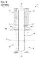
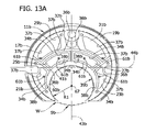
ウエハWに対するクランプ力は、自由領域60aでは実際上ゼロである。これらの特徴を以下に更に説明する。
更に、各々のポケットに関連する領域の剛性(stiffness)は、ポケット深さを異ならせることによって、ポケットの間で変えることができる。深いポケットは、深いポケットの領域において、浅いポケットに比べてウエハWの柔軟な(compliant)保持をもたらし、浅いポケットの領域においてウエハを強固に保持する。
研削サイクルおよび、プロセッサ351が有限要素構造分析のためのデータを収集する時間は、本発明の技術的範囲から逸脱せずに変更可能である。
(態様1)
一対の研削砥石と、その中に静水圧を有する一対の静水圧パッドとの間にウエハを保持するタイプの両面研削盤を用いて半導体ウエハを処理する方法であって、研削盤は、研削盤によって引き込まれた電流を検出するためのパターン検出ソフトウェアを含むプロセッサを含んでおり、該方法は、
ウエハをクランプする段階と、
ウエハを研削する段階と、
ウエハを研削砥石との接触から離す段階と、
各々の段階を検出するためのソフトウェアを使用し、各々の段階における静水圧を変えて、ウエハに適用されるクランプ圧力を変え、それにより処理したウエハのナノトポロジーを改善する段階と、の複数の段階を含む方法。
(態様2)
流量制御弁を通過する流速を変えることによって静水圧を変える、態様1に記載の方法。
(態様3)
各々の段階を検出するために、研削盤によって引き込まれる電流をパターン検出ソフトウェアで測定する、態様1に記載の方法。
(態様4)
研削段階において、静水圧を低下させることを更に含む、態様1に記載の方法。
(態様5)
研削段階において、静水圧を上昇させることを更に含む、態様1に記載の方法。
(態様6)
研削操作中に一対の研削砥石と一対の静水圧パッドとの間にウエハを保持するタイプの両面研削盤を用いて半導体ウエハを処理する方法であって、該方法は、
研削操作の第1段階において、静水圧パッド内に第1静水圧を確立してウエハを最初にクランプすることと、
研削操作の第2段階でウエハを研削する間に、第1圧力よりも低い第2静水圧まで静水圧を低下させることと、
研削操作の第3段階において第3静水圧まで静水圧を上昇させてウエハをクランプし、これにより処理されたウエハのナノトポロジーを改善することと、を含む方法。
(態様7)
第3静水圧は第1静水圧と実質的に等しい、態様6に記載の方法。
(態様8)
ウエハの研削中に、研削砥石によってウエハを実質的にクランプする、態様6に記載の方法。
(態様9)
静水圧を、流量制御弁の使用によって変える、態様6に記載の方法。
(態様10)
ウエハを、実質的に垂直な平面内で保持する、態様6に記載の方法。
(態様11)
両面研削盤の研削砥石によって使用される電流量を測定することを更に含む、態様6に記載の方法。
(態様12)
両面研削盤の研削砥石によって使用される、測定された電流量に基づいて、研削操作の段階を決めることを更に含む、態様11に記載の方法。
(態様13)
測定された電流が残留状態から初期状態まで増加したときに、研削操作の段階が第1段階であると決めることを更に含む、態様12に記載の方法。
(態様14)
測定された電流がそのピークレベルであるときに、研削操作の段階が第2段階であると決めることを更に含む、態様12に記載の方法。
(態様15)
測定された電流がそのピークレベルから減少したときに、研削操作の段階が第3段階であると決めることを更に含む、態様14に記載の方法。
(態様16)
一対の研削砥石と、プロセッサと、一対の静水圧パッドとを含む両面研削盤であって、
研削砥石と静水圧パッドとは、ほぼ平坦なウエハを、一対の研削砥石の間に配置されているウエハの第1部分と一対の静水圧パッドの間に配置されているウエハの第2部分とが同一平面内で保持されるように操作可能であり、
静水圧パッドは、静水圧を維持するように静水圧パッドを通過して流れる水を含み、
研削盤は、パッドを通過する水の流速を制御するための、それにより静水圧を制御するための、流量制御弁を更に含み、
流量制御弁は、プロセッサによって制御される、両面研削盤。
(態様17)
プロセッサが、研削プロセスの様々な段階を検出するためのパターン検出ソフトウェアを含んでおり、該プロセッサは、パターン検出ソフトウェアによって検出された段階に応じて、流量制御弁を通過する水の流速を制御するように動作可能である、態様16に記載の研削盤。
(態様18)
プロセッサが、研削砥石によって使用される電流量を測定するように動作可能である、態様17に記載の研削盤。
(態様19)
パターン検出ソフトウェアは、研削砥石によって使用される、測定された電気量に基づいて段階を検出する、態様18に記載の研削盤。
(態様20)
プロセッサは、パターン検出ソフトウェアが研削プロセスの研削段階を検出したときに、弁を通過する水の流速を増加するように流量制御弁を制御する、態様19に記載の研削盤。
Claims (10)
- 両面研磨盤により行われる研削操作の間に、一対の研削砥石と一対の静水圧パッドとの間にウエハを保持する種類の両面研削盤を用いて半導体ウエハを処理する方法であって、該方法が
研削操作の第1段階において、静水圧パッド内に第1静水圧を確立してウエハを最初にクランプすること、
両面研削盤の研削砥石によって使用される電流量を測定すること、
両面研削盤の研削砥石によって使用される、測定された電流量に基づいて、研削操作の3つの段階の1つを決定すること、
研削操作の第2段階でウエハを研削する間に、第1静水圧よりも低い第2静水圧まで静水圧を低下させること、および
研削操作の第3段階の間において、第3静水圧まで静水圧を上昇させて、静水圧パッドによりウエハをクランプし、それにより、処理されたウエハにおけるナノトポロジーを改善すること、を含み、
第1段階は、ウエハが静水圧パッドによってクランプされる最初の期間に対応し、
第2段階は、研削操作が除去する間のうち、最も多くの材料が除去される第2の期間に対応する、
方法。 - 第3静水圧が、第1静水圧と等しい、請求項1に記載の方法。
- 第2段階において、ウエハを研削する間、研削砥石によってウエハをクランプする、請求項1に記載の方法。
- 流れ制御弁を使用することによって静水圧を変更する、請求項1に記載の方法。
- ウエハを、垂直な平面上に保持する、請求項1に記載の方法。
- 測定された電流が残留状態から初期状態まで増加したときに、研削操作の段階が第1段階であると決定することを更に含む、請求項1に記載の方法。
- 測定された電流がそのピークレベルである場合に、研削操作の段階が第2段階であると決めることを更に含む、請求項1に記載の方法。
- 測定された電流がそのピークレベルから減少したときに、研削操作の段階が第3段階であると決定することを更に含み、
測定された電流がそのピークレベルから減少したとの決定に応じて、静水圧を増加する、請求項7に記載の方法。 - 一対の研削砥石と、プロセッサと、一対の静水圧パッドと、流れ制御弁と、を含む両面研削盤であって、
研削砥石と静水圧パッドとが、一対の研削砥石の間に配置されたウエハの第1部分および一対の静水圧パッドの間に配置されたウエハの第2部分とを備えた平坦なウエハとを同一平面で保持するように作動でき、
プロセッサが、研削砥石によって使用される電流量を測定するように作動し、
静水圧パッドが、静水圧を維持するようにそこを通過して流れる水を含み、
流れ制御弁が、パッドを通過する水の流速を制御しそれにより静水圧を制御するように作動し、
プロセッサは、研削砥石によって使用される、測定された電気量に基づいて、切削プロセスの段階を検出するパターン検出ソフトウェアプログラムを実行し、
プロセッサは、パターン検出ソフトウェアプログラムによって検出された段階に応じて、流れ制御弁を通過する水の流速を制御するように作動する両面研削盤。 - パターン検出ソフトウェアプログラムが研削プロセスの研削段階を検出した場合に、プロセッサが、弁を通過する水の流速を増加するように流れ制御弁を制御する、請求項9に記載の研削盤。
Applications Claiming Priority (3)
| Application Number | Priority Date | Filing Date | Title |
|---|---|---|---|
| US31791910P | 2010-03-26 | 2010-03-26 | |
| US61/317,919 | 2010-03-26 | ||
| PCT/IB2011/051152 WO2011117792A1 (en) | 2010-03-26 | 2011-03-18 | Hydrostatic pad pressure modulation in a simultaneous double side wafer grinder |
Publications (3)
| Publication Number | Publication Date |
|---|---|
| JP2013524484A JP2013524484A (ja) | 2013-06-17 |
| JP2013524484A5 JP2013524484A5 (ja) | 2015-10-15 |
| JP6013317B2 true JP6013317B2 (ja) | 2016-10-25 |
Family
ID=44657008
Family Applications (1)
| Application Number | Title | Priority Date | Filing Date |
|---|---|---|---|
| JP2013500633A Active JP6013317B2 (ja) | 2010-03-26 | 2011-03-18 | 同時両面ウエハ研削盤における静水圧パッド圧力調節 |
Country Status (8)
| Country | Link |
|---|---|
| US (1) | US8712575B2 (ja) |
| EP (1) | EP2552644A4 (ja) |
| JP (1) | JP6013317B2 (ja) |
| KR (1) | KR101694574B1 (ja) |
| CN (1) | CN102844151A (ja) |
| SG (1) | SG184014A1 (ja) |
| TW (1) | TWI520202B (ja) |
| WO (1) | WO2011117792A1 (ja) |
Families Citing this family (15)
| Publication number | Priority date | Publication date | Assignee | Title |
|---|---|---|---|---|
| US9358660B2 (en) | 2011-11-07 | 2016-06-07 | Taiwan Semiconductor Manufacturing Company, Ltd. | Grinding wheel design with elongated teeth arrangement |
| US9960088B2 (en) * | 2011-11-07 | 2018-05-01 | Taiwan Semiconductor Manufacturing Company, Ltd. | End point detection in grinding |
| JP6197580B2 (ja) * | 2013-10-29 | 2017-09-20 | 株式会社Sumco | キャリアプレート及びワークの両面研磨装置 |
| CN105881213A (zh) * | 2014-09-01 | 2016-08-24 | 曾庆明 | 一种精密双面研磨机的控制器 |
| JP6285375B2 (ja) * | 2015-02-17 | 2018-02-28 | 光洋機械工業株式会社 | 両頭平面研削装置 |
| JP6447472B2 (ja) * | 2015-11-26 | 2019-01-09 | 株式会社Sumco | ウェーハ研磨方法 |
| CN108127560A (zh) * | 2017-12-08 | 2018-06-08 | 中国兵器科学研究院宁波分院 | 用于方形光学元件双面快速抛光的控制系统 |
| JP6513174B2 (ja) * | 2017-12-25 | 2019-05-15 | 信越半導体株式会社 | ウェーハ保持用キャリアの設計方法 |
| JP7159861B2 (ja) * | 2018-12-27 | 2022-10-25 | 株式会社Sumco | 両頭研削方法 |
| JP7116371B2 (ja) * | 2019-04-01 | 2022-08-10 | 株式会社村田製作所 | 研磨剤供給装置、研磨装置及び研磨剤供給方法 |
| US11415971B2 (en) | 2020-02-10 | 2022-08-16 | Globalwafers Co., Ltd. | Systems and methods for enhanced wafer manufacturing |
| CN114227524A (zh) * | 2021-12-30 | 2022-03-25 | 西安奕斯伟材料科技有限公司 | 双面研磨装置和双面研磨方法 |
| CN115070604B (zh) * | 2022-06-09 | 2023-09-29 | 西安奕斯伟材料科技股份有限公司 | 双面研磨装置和双面研磨方法 |
| CN115723035B (zh) * | 2022-09-08 | 2024-05-28 | 西安奕斯伟材料科技股份有限公司 | 用于监控研磨装置的加工状态的系统、方法及双面研磨装置 |
| TWI832517B (zh) * | 2022-09-22 | 2024-02-11 | 大陸商西安奕斯偉材料科技股份有限公司 | 研磨裝置、研磨方法及矽片 |
Family Cites Families (37)
| Publication number | Priority date | Publication date | Assignee | Title |
|---|---|---|---|---|
| JPH1177497A (ja) * | 1997-09-01 | 1999-03-23 | Waida Seisakusho:Kk | 半導体ウエハの両面研削方法及び両面研削装置 |
| JPH11154655A (ja) * | 1997-11-21 | 1999-06-08 | Komatsu Electron Metals Co Ltd | 半導体ウェハの製造方法 |
| JP3328193B2 (ja) * | 1998-07-08 | 2002-09-24 | 信越半導体株式会社 | 半導体ウエーハの製造方法 |
| JP3664593B2 (ja) * | 1998-11-06 | 2005-06-29 | 信越半導体株式会社 | 半導体ウエーハおよびその製造方法 |
| WO2000067950A1 (fr) * | 1999-05-07 | 2000-11-16 | Shin-Etsu Handotai Co.,Ltd. | Procedes et dispositifs correspondants permettant de meuler et de roder des surfaces doubles simultanement |
| US6294469B1 (en) * | 1999-05-21 | 2001-09-25 | Plasmasil, Llc | Silicon wafering process flow |
| JP2002307303A (ja) * | 2001-04-10 | 2002-10-23 | Koyo Mach Ind Co Ltd | 薄板円板状ワークの両面研削方法および装置 |
| JP2002307275A (ja) * | 2001-04-16 | 2002-10-23 | Sumitomo Heavy Ind Ltd | 加工システム及び面取り装置 |
| JP2002346924A (ja) * | 2001-05-29 | 2002-12-04 | Sumitomo Heavy Ind Ltd | ワークホルダ |
| JP3848120B2 (ja) * | 2001-10-12 | 2006-11-22 | 住友重機械工業株式会社 | ワーク研削装置 |
| JP2004072076A (ja) * | 2002-06-10 | 2004-03-04 | Nikon Corp | 露光装置及びステージ装置、並びにデバイス製造方法 |
| KR100954534B1 (ko) * | 2002-10-09 | 2010-04-23 | 고요 기카이 고교 가부시키가이샤 | 얇은 원판형상 공작물의 양면 연삭방법 및 양면 연삭장치 |
| JP3993856B2 (ja) * | 2004-01-22 | 2007-10-17 | 光洋機械工業株式会社 | 両頭平面研削装置 |
| JP4326974B2 (ja) * | 2004-01-30 | 2009-09-09 | コマツNtc株式会社 | ウェーハの研削装置及び研削方法 |
| DE102004005702A1 (de) * | 2004-02-05 | 2005-09-01 | Siltronic Ag | Halbleiterscheibe, Vorrichtung und Verfahren zur Herstellung der Halbleiterscheibe |
| US8066553B2 (en) * | 2004-03-19 | 2011-11-29 | Memc Electronic Materials, Inc. | Wafer clamping device for a double side grinder |
| US7040958B2 (en) * | 2004-05-21 | 2006-05-09 | Mosel Vitelic, Inc. | Torque-based end point detection methods for chemical mechanical polishing tool which uses ceria-based CMP slurry to polish to protective pad layer |
| JP4615275B2 (ja) * | 2004-09-21 | 2011-01-19 | 株式会社ディスコ | ウェーハ研磨装置及びウェーハの研磨方法 |
| JP4670566B2 (ja) * | 2005-09-29 | 2011-04-13 | 信越半導体株式会社 | 半導体ウェーハの両頭研削装置、静圧パッドおよびこれを用いた両頭研削方法 |
| JP4752475B2 (ja) * | 2005-12-08 | 2011-08-17 | 信越半導体株式会社 | 半導体ウェーハの両頭研削装置、静圧パッドおよびこれを用いた両頭研削方法 |
| US7930058B2 (en) * | 2006-01-30 | 2011-04-19 | Memc Electronic Materials, Inc. | Nanotopography control and optimization using feedback from warp data |
| JP5518338B2 (ja) * | 2006-01-30 | 2014-06-11 | エムイーエムシー・エレクトロニック・マテリアルズ・インコーポレイテッド | 加工対象物のナノトポロジを評価するためのウェハ両面グラインダ及び方法 |
| US7601049B2 (en) * | 2006-01-30 | 2009-10-13 | Memc Electronic Materials, Inc. | Double side wafer grinder and methods for assessing workpiece nanotopology |
| US7662023B2 (en) * | 2006-01-30 | 2010-02-16 | Memc Electronic Materials, Inc. | Double side wafer grinder and methods for assessing workpiece nanotopology |
| EP1870936A1 (fr) * | 2006-06-19 | 2007-12-26 | STMicroelectronics (Rousset) SAS | Procédé de fabrication de lentilles, notamment pour imageur intégré |
| JP5177430B2 (ja) * | 2006-07-18 | 2013-04-03 | Jsr株式会社 | 化学機械研磨用水系分散体、その製造方法および化学機械研磨方法 |
| DE102007030958B4 (de) * | 2007-07-04 | 2014-09-11 | Siltronic Ag | Verfahren zum Schleifen von Halbleiterscheiben |
| US8012857B2 (en) * | 2007-08-07 | 2011-09-06 | Semiconductor Components Industries, Llc | Semiconductor die singulation method |
| US7989319B2 (en) * | 2007-08-07 | 2011-08-02 | Semiconductor Components Industries, Llc | Semiconductor die singulation method |
| US8859396B2 (en) * | 2007-08-07 | 2014-10-14 | Semiconductor Components Industries, Llc | Semiconductor die singulation method |
| JP5245319B2 (ja) * | 2007-08-09 | 2013-07-24 | 富士通株式会社 | 研磨装置及び研磨方法、基板及び電子機器の製造方法 |
| DE102007049811B4 (de) * | 2007-10-17 | 2016-07-28 | Peter Wolters Gmbh | Läuferscheibe, Verfahren zur Beschichtung einer Läuferscheibe sowie Verfahren zur gleichzeitigen beidseitigen Material abtragenden Bearbeitung von Halbleiterscheiben |
| JP4985451B2 (ja) * | 2008-02-14 | 2012-07-25 | 信越半導体株式会社 | ワークの両頭研削装置およびワークの両頭研削方法 |
| JP5390807B2 (ja) * | 2008-08-21 | 2014-01-15 | 株式会社荏原製作所 | 研磨方法および装置 |
| JP2010064214A (ja) * | 2008-09-12 | 2010-03-25 | Koyo Mach Ind Co Ltd | 両頭平面研削盤及びワークの両面研削方法 |
| JP4291405B1 (ja) * | 2008-11-14 | 2009-07-08 | 健治 吉田 | ドットパターン読み取り機能を備えたマウス |
| DE102009048436B4 (de) * | 2009-10-07 | 2012-12-20 | Siltronic Ag | Verfahren zum Schleifen einer Halbleiterscheibe |
-
2011
- 2011-03-16 US US13/049,536 patent/US8712575B2/en active Active
- 2011-03-18 JP JP2013500633A patent/JP6013317B2/ja active Active
- 2011-03-18 SG SG2012067369A patent/SG184014A1/en unknown
- 2011-03-18 WO PCT/IB2011/051152 patent/WO2011117792A1/en active Application Filing
- 2011-03-18 KR KR1020127025126A patent/KR101694574B1/ko active IP Right Grant
- 2011-03-18 CN CN201180016139XA patent/CN102844151A/zh active Pending
- 2011-03-18 EP EP11758894.7A patent/EP2552644A4/en not_active Withdrawn
- 2011-03-25 TW TW100110457A patent/TWI520202B/zh active
Also Published As
| Publication number | Publication date |
|---|---|
| SG184014A1 (en) | 2012-10-30 |
| TWI520202B (zh) | 2016-02-01 |
| WO2011117792A1 (en) | 2011-09-29 |
| KR20130008572A (ko) | 2013-01-22 |
| KR101694574B1 (ko) | 2017-01-09 |
| JP2013524484A (ja) | 2013-06-17 |
| EP2552644A1 (en) | 2013-02-06 |
| TW201201264A (en) | 2012-01-01 |
| US8712575B2 (en) | 2014-04-29 |
| EP2552644A4 (en) | 2014-05-14 |
| US20110237160A1 (en) | 2011-09-29 |
| CN102844151A (zh) | 2012-12-26 |
Similar Documents
| Publication | Publication Date | Title |
|---|---|---|
| JP6013317B2 (ja) | 同時両面ウエハ研削盤における静水圧パッド圧力調節 | |
| JP2013524484A5 (ja) | ||
| US7927185B2 (en) | Method for assessing workpiece nanotopology using a double side wafer grinder | |
| EP2225070B1 (en) | Nanotopography control and optimization using feedback from warp data | |
| KR101141474B1 (ko) | 양면 연삭기용 웨이퍼 클램핑 장치 | |
| CN100364062C (zh) | 同时双面研磨晶片形工件的装置 | |
| US7601049B2 (en) | Double side wafer grinder and methods for assessing workpiece nanotopology | |
| TWI381906B (zh) | 雙面晶圓研磨器及評估工作件奈米布局之方法 | |
| JPH11245162A (ja) | 平面の作業面を有する工具 | |
| WO2021059790A1 (ja) | ワークの両面研磨方法 | |
| KR20230003312A (ko) | 워크의 양면 연마 방법, 워크의 제조 방법 및, 워크의 양면 연마 장치 |
Legal Events
| Date | Code | Title | Description |
|---|---|---|---|
| A521 | Request for written amendment filed |
Free format text: JAPANESE INTERMEDIATE CODE: A523 Effective date: 20140317 |
|
| A621 | Written request for application examination |
Free format text: JAPANESE INTERMEDIATE CODE: A621 Effective date: 20140317 |
|
| A977 | Report on retrieval |
Free format text: JAPANESE INTERMEDIATE CODE: A971007 Effective date: 20150313 |
|
| A131 | Notification of reasons for refusal |
Free format text: JAPANESE INTERMEDIATE CODE: A131 Effective date: 20150324 |
|
| A601 | Written request for extension of time |
Free format text: JAPANESE INTERMEDIATE CODE: A601 Effective date: 20150622 |
|
| A601 | Written request for extension of time |
Free format text: JAPANESE INTERMEDIATE CODE: A601 Effective date: 20150724 |
|
| A524 | Written submission of copy of amendment under article 19 pct |
Free format text: JAPANESE INTERMEDIATE CODE: A524 Effective date: 20150824 |
|
| RD04 | Notification of resignation of power of attorney |
Free format text: JAPANESE INTERMEDIATE CODE: A7424 Effective date: 20160216 |
|
| A131 | Notification of reasons for refusal |
Free format text: JAPANESE INTERMEDIATE CODE: A131 Effective date: 20160329 |
|
| A521 | Request for written amendment filed |
Free format text: JAPANESE INTERMEDIATE CODE: A523 Effective date: 20160603 |
|
| TRDD | Decision of grant or rejection written | ||
| A01 | Written decision to grant a patent or to grant a registration (utility model) |
Free format text: JAPANESE INTERMEDIATE CODE: A01 Effective date: 20160913 |
|
| A61 | First payment of annual fees (during grant procedure) |
Free format text: JAPANESE INTERMEDIATE CODE: A61 Effective date: 20160921 |
|
| R150 | Certificate of patent or registration of utility model |
Ref document number: 6013317 Country of ref document: JP Free format text: JAPANESE INTERMEDIATE CODE: R150 |
|
| R250 | Receipt of annual fees |
Free format text: JAPANESE INTERMEDIATE CODE: R250 |
|
| S111 | Request for change of ownership or part of ownership |
Free format text: JAPANESE INTERMEDIATE CODE: R313113 |
|
| S531 | Written request for registration of change of domicile |
Free format text: JAPANESE INTERMEDIATE CODE: R313531 |
|
| S533 | Written request for registration of change of name |
Free format text: JAPANESE INTERMEDIATE CODE: R313533 |
|
| R350 | Written notification of registration of transfer |
Free format text: JAPANESE INTERMEDIATE CODE: R350 |
|
| R250 | Receipt of annual fees |
Free format text: JAPANESE INTERMEDIATE CODE: R250 |
|
| R250 | Receipt of annual fees |
Free format text: JAPANESE INTERMEDIATE CODE: R250 |
|
| R250 | Receipt of annual fees |
Free format text: JAPANESE INTERMEDIATE CODE: R250 |
|
| R250 | Receipt of annual fees |
Free format text: JAPANESE INTERMEDIATE CODE: R250 |