JP5924909B2 - 配線回路基板およびその製造方法 - Google Patents
配線回路基板およびその製造方法 Download PDFInfo
- Publication number
- JP5924909B2 JP5924909B2 JP2011254039A JP2011254039A JP5924909B2 JP 5924909 B2 JP5924909 B2 JP 5924909B2 JP 2011254039 A JP2011254039 A JP 2011254039A JP 2011254039 A JP2011254039 A JP 2011254039A JP 5924909 B2 JP5924909 B2 JP 5924909B2
- Authority
- JP
- Japan
- Prior art keywords
- line
- insulating layer
- wiring pattern
- lines
- electrically connected
- Prior art date
- Legal status (The legal status is an assumption and is not a legal conclusion. Google has not performed a legal analysis and makes no representation as to the accuracy of the status listed.)
- Active
Links
Images


Classifications
-
- G—PHYSICS
- G11—INFORMATION STORAGE
- G11B—INFORMATION STORAGE BASED ON RELATIVE MOVEMENT BETWEEN RECORD CARRIER AND TRANSDUCER
- G11B5/00—Recording by magnetisation or demagnetisation of a record carrier; Reproducing by magnetic means; Record carriers therefor
- G11B5/48—Disposition or mounting of heads or head supports relative to record carriers ; arrangements of heads, e.g. for scanning the record carrier to increase the relative speed
- G11B5/4806—Disposition or mounting of heads or head supports relative to record carriers ; arrangements of heads, e.g. for scanning the record carrier to increase the relative speed specially adapted for disk drive assemblies, e.g. assembly prior to operation, hard or flexible disk drives
- G11B5/486—Disposition or mounting of heads or head supports relative to record carriers ; arrangements of heads, e.g. for scanning the record carrier to increase the relative speed specially adapted for disk drive assemblies, e.g. assembly prior to operation, hard or flexible disk drives with provision for mounting or arranging electrical conducting means or circuits on or along the arm assembly
-
- G—PHYSICS
- G11—INFORMATION STORAGE
- G11B—INFORMATION STORAGE BASED ON RELATIVE MOVEMENT BETWEEN RECORD CARRIER AND TRANSDUCER
- G11B5/00—Recording by magnetisation or demagnetisation of a record carrier; Reproducing by magnetic means; Record carriers therefor
- G11B5/48—Disposition or mounting of heads or head supports relative to record carriers ; arrangements of heads, e.g. for scanning the record carrier to increase the relative speed
- G11B5/4806—Disposition or mounting of heads or head supports relative to record carriers ; arrangements of heads, e.g. for scanning the record carrier to increase the relative speed specially adapted for disk drive assemblies, e.g. assembly prior to operation, hard or flexible disk drives
- G11B5/484—Integrated arm assemblies, e.g. formed by material deposition or by etching from single piece of metal or by lamination of materials forming a single arm/suspension/head unit
-
- H—ELECTRICITY
- H05—ELECTRIC TECHNIQUES NOT OTHERWISE PROVIDED FOR
- H05K—PRINTED CIRCUITS; CASINGS OR CONSTRUCTIONAL DETAILS OF ELECTRIC APPARATUS; MANUFACTURE OF ASSEMBLAGES OF ELECTRICAL COMPONENTS
- H05K1/00—Printed circuits
- H05K1/02—Details
- H05K1/0213—Electrical arrangements not otherwise provided for
- H05K1/0237—High frequency adaptations
- H05K1/0245—Lay-out of balanced signal pairs, e.g. differential lines or twisted lines
-
- G—PHYSICS
- G11—INFORMATION STORAGE
- G11B—INFORMATION STORAGE BASED ON RELATIVE MOVEMENT BETWEEN RECORD CARRIER AND TRANSDUCER
- G11B5/00—Recording by magnetisation or demagnetisation of a record carrier; Reproducing by magnetic means; Record carriers therefor
- G11B5/48—Disposition or mounting of heads or head supports relative to record carriers ; arrangements of heads, e.g. for scanning the record carrier to increase the relative speed
- G11B5/4806—Disposition or mounting of heads or head supports relative to record carriers ; arrangements of heads, e.g. for scanning the record carrier to increase the relative speed specially adapted for disk drive assemblies, e.g. assembly prior to operation, hard or flexible disk drives
- G11B5/4853—Constructional details of the electrical connection between head and arm
-
- H—ELECTRICITY
- H05—ELECTRIC TECHNIQUES NOT OTHERWISE PROVIDED FOR
- H05K—PRINTED CIRCUITS; CASINGS OR CONSTRUCTIONAL DETAILS OF ELECTRIC APPARATUS; MANUFACTURE OF ASSEMBLAGES OF ELECTRICAL COMPONENTS
- H05K1/00—Printed circuits
- H05K1/02—Details
- H05K1/0213—Electrical arrangements not otherwise provided for
- H05K1/0237—High frequency adaptations
- H05K1/0248—Skew reduction or using delay lines
-
- Y—GENERAL TAGGING OF NEW TECHNOLOGICAL DEVELOPMENTS; GENERAL TAGGING OF CROSS-SECTIONAL TECHNOLOGIES SPANNING OVER SEVERAL SECTIONS OF THE IPC; TECHNICAL SUBJECTS COVERED BY FORMER USPC CROSS-REFERENCE ART COLLECTIONS [XRACs] AND DIGESTS
- Y10—TECHNICAL SUBJECTS COVERED BY FORMER USPC
- Y10T—TECHNICAL SUBJECTS COVERED BY FORMER US CLASSIFICATION
- Y10T29/00—Metal working
- Y10T29/49—Method of mechanical manufacture
- Y10T29/49002—Electrical device making
- Y10T29/49117—Conductor or circuit manufacturing
- Y10T29/49124—On flat or curved insulated base, e.g., printed circuit, etc.
- Y10T29/49126—Assembling bases
-
- Y—GENERAL TAGGING OF NEW TECHNOLOGICAL DEVELOPMENTS; GENERAL TAGGING OF CROSS-SECTIONAL TECHNOLOGIES SPANNING OVER SEVERAL SECTIONS OF THE IPC; TECHNICAL SUBJECTS COVERED BY FORMER USPC CROSS-REFERENCE ART COLLECTIONS [XRACs] AND DIGESTS
- Y10—TECHNICAL SUBJECTS COVERED BY FORMER USPC
- Y10T—TECHNICAL SUBJECTS COVERED BY FORMER US CLASSIFICATION
- Y10T29/00—Metal working
- Y10T29/49—Method of mechanical manufacture
- Y10T29/49002—Electrical device making
- Y10T29/49117—Conductor or circuit manufacturing
- Y10T29/49124—On flat or curved insulated base, e.g., printed circuit, etc.
- Y10T29/4913—Assembling to base an electrical component, e.g., capacitor, etc.
- Y10T29/49146—Assembling to base an electrical component, e.g., capacitor, etc. with encapsulating, e.g., potting, etc.
-
- Y—GENERAL TAGGING OF NEW TECHNOLOGICAL DEVELOPMENTS; GENERAL TAGGING OF CROSS-SECTIONAL TECHNOLOGIES SPANNING OVER SEVERAL SECTIONS OF THE IPC; TECHNICAL SUBJECTS COVERED BY FORMER USPC CROSS-REFERENCE ART COLLECTIONS [XRACs] AND DIGESTS
- Y10—TECHNICAL SUBJECTS COVERED BY FORMER USPC
- Y10T—TECHNICAL SUBJECTS COVERED BY FORMER US CLASSIFICATION
- Y10T29/00—Metal working
- Y10T29/49—Method of mechanical manufacture
- Y10T29/49002—Electrical device making
- Y10T29/49117—Conductor or circuit manufacturing
- Y10T29/49124—On flat or curved insulated base, e.g., printed circuit, etc.
- Y10T29/49155—Manufacturing circuit on or in base
Landscapes
- Engineering & Computer Science (AREA)
- Microelectronics & Electronic Packaging (AREA)
- Structure Of Printed Boards (AREA)
- Adjustment Of The Magnetic Head Position Track Following On Tapes (AREA)
- Supporting Of Heads In Record-Carrier Devices (AREA)
- Insulated Metal Substrates For Printed Circuits (AREA)
Description
また、第1の絶縁層は、第4の線路と接続層との間に第1の貫通孔を有し、かつ第6の線路と接続層との間に第2の貫通孔を有し、第4の線路は、第1の貫通孔を通して接続層と電気的に接続され、第6の線路は、第2の貫通孔を通して接続層と電気的に接続される。第3の線路は、第1の貫通孔に干渉しない。
この場合、第4の線路は、第1の絶縁層の第1の貫通孔を通して接続層に電気的に接続される。また、第6の線路は、第1の絶縁層の第2の貫通孔を通して接続層に電気的に接続される。これにより、第2の配線パターンの分岐部分の占有面積を小さくすることができる。その結果、配線回路基板を小型化することができる。
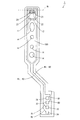
図1は、本発明の一実施の形態に係るサスペンション基板の上面図である。図1に示すように、サスペンション基板1は、金属製の長尺状の支持基板により形成されるサスペンション本体部100を備える。サスペンション本体部100上には、太い点線で示すように、書込用配線パターンW1,W2および読取用配線パターンR1,R2が形成されている。書込用配線パターンW1と書込用配線パターンW2とは、信号線路対を構成する。また、読取用配線パターンR1と読取用配線パターンR2とは、信号線路対を構成する。
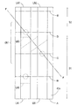
次に、書込用配線パターンW1,W2の詳細な構成について説明する。図2は、書込用配線パターンW1,W2の構成を示す平面図である。図3は、図2のサスペンション基板1のX部の透視的な斜視図である。
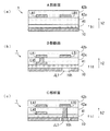
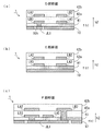
次に、サスペンション基板1の製造方法について説明する。図9〜図12は、サスペンション基板1の製造工程を示す縦断面図である。ここで、図9(a)〜図12(b)の上段に図2のサスペンション基板1のC部断面の製造工程を示し、下段に図2のサスペンション基板1のD部断面の製造工程を示す。
本実施の形態においては、書込用配線パターンW1の線路LA1,LA2および書込用配線パターンW2の線路LB1,LB2がカバー絶縁層42aの上面上に配置される。書込用配線パターンW1の線路LA3および書込用配線パターンW2の線路LB3がベース絶縁層41の上面上に配置される。線路LA2,LA3が線路LA1と電気的に接続されることにより、線路LA1が線路LA2と線路LA3とに分岐する。線路LB2,LB3が線路LB1と電気的に接続されることにより、線路LB1が線路LB2と線路LB3とに分岐する。
(5−1)上記実施の形態において配線回路基板はサスペンション基板1であるが、これに限定されない。配線回路基板は、フレキシブル配線回路基板等の他の配線回路基板であってもよい。この場合、配線回路基板は支持基板10を含まないので、ジャンパー配線JL1,JL2は支持基板10の一部としてではなく、別個に形成される。
以下、請求項の各構成要素と実施の形態の各部との対応の例について説明するが、本発明は下記の例に限定されない。
10 支持基板
11 開口部
12 タング部
21〜24,31〜34 電極パッド
41 ベース絶縁層
42a,42b カバー絶縁層
100 サスペンション本体部
CN1,CN2 交差領域
D1 第1の領域
D2 第2の領域
D3 第3の領域
H 孔部
H1〜H3 貫通孔
JL1,JL2 ジャンパー配線
LA1〜LA5,LB1〜LB5 線路
R 破線
R1,R2 読取用配線パターン
RG1 島状領域
W1,W2 書込用配線パターン
Claims (5)
- 第1および第2の面を有する第1の絶縁層と、
第3および第4の面を有し、前記第4の面が前記第1の面に接するように前記第1の絶縁層上に形成される第2の絶縁層と、
前記第1の絶縁層の前記第1の面上および前記第2の絶縁層の前記第3の面上に形成され、信号線路対を構成する第1および第2の配線パターンと、
前記第1の絶縁層の前記第2の面上に形成される導電性の接続層とを備え、
前記第1の配線パターンは、
前記第1の絶縁層の前記第1の面上または前記第2の絶縁層の前記第3の面上に配置される第1の線路と、
前記第2の絶縁層の前記第3の面上に配置され、前記第1の線路と電気的に接続される第2の線路と、
前記第1の絶縁層の前記第1の面上に配置され、前記第1の線路と電気的に接続される第3の線路とを含み、
前記第2の配線パターンは、
前記第1の絶縁層の前記第1の面上または前記第2の絶縁層の前記第3の面上に配置される第4の線路と、
前記第2の絶縁層の前記第3の面上に配置され、前記第4の線路と電気的に接続される第5の線路と、
前記第1の絶縁層の前記第1の面上に配置され、前記第4の線路と電気的に接続される第6の線路とを含み、
前記第2の線路の少なくとも一部は、前記第2の絶縁層を介して前記第6の線路に対向するように配置され、
前記第5の線路の少なくとも一部は、前記第2の絶縁層を介して前記第3の線路に対向するように配置され、
前記第4の線路は、前記接続層を通して前記第6の線路と電気的に接続され、
前記第1の絶縁層は、前記第4の線路と前記接続層との間に第1の貫通孔を有し、かつ前記第6の線路と前記接続層との間に第2の貫通孔を有し、前記第4の線路は、前記第1の貫通孔を通して前記接続層と電気的に接続され、前記第6の線路は、前記第2の貫通孔を通して前記接続層と電気的に接続され、
前記第3の線路は、前記第1の貫通孔に干渉しないように配置される、配線回路基板。 - 前記第1の線路および前記第4の線路は、前記第2の絶縁層の前記第3の面上に形成される、請求項1記載の配線回路基板。
- 前記第1の線路および前記第4の線路は、前記第1の絶縁層の前記第1の面上に形成される、請求項1記載の配線回路基板。
- 前記第1の線路および前記第4の線路の一方は、前記第1の絶縁層の前記第1の面上に形成され、前記第1の線路および前記第4の線路の他方は、前記第2の絶縁層の前記第3の面上に形成される、請求項1記載の配線回路基板。
- 第1および第2の面を有する第1の絶縁層上に第3および第4の面を有する第2の絶縁層を前記第4の面が前記第1の面に接するように形成する工程と、
前記第1の絶縁層の前記第1の面上および前記第2の絶縁層の前記第3の面上に信号線路対を構成する第1および第2の配線パターンを形成する工程と、
前記第1の絶縁層の前記第2の面上に導電性の接続層を形成する工程とを備え、
前記第1の配線パターンを形成する工程は、
前記第2の絶縁層の前記第3の面上に第2の線路を形成する工程と、
前記第1の絶縁層の前記第1の面上に第3の線路を形成する工程と、
前記第1の絶縁層の前記第1の面上または前記第2の絶縁層の前記第3の面上に第1の線路を形成する工程とを含み、
前記第2および第3の線路は前記第1の線路と電気的に接続され、
前記第2の配線パターンを形成する工程は、
前記第2の絶縁層の前記第3の面上に第5の線路を形成する工程と、
前記第1の絶縁層の前記第1の面上に第6の線路を形成する工程と、
前記第1の絶縁層の前記第1の面上または前記第2の絶縁層の前記第3の面上に第4の線路を形成する工程とを含み、
前記第5および第6の線路は前記第4の線路と電気的に接続され、
前記第2の線路の少なくとも一部は、前記第2の絶縁層を介して前記第6の線路に対向するように配置され、
前記第5の線路の少なくとも一部は、前記第2の絶縁層を介して前記第3の線路に対向するように配置され、
前記第4の線路は、前記接続層を通して前記第6の線路と電気的に接続され、
前記第1の絶縁層は、前記第4の線路と前記接続層との間に第1の貫通孔を有し、かつ前記第6の線路と前記接続層との間に第2の貫通孔を有し、前記第4の線路は、前記第1の貫通孔を通して前記接続層と電気的に接続され、前記第6の線路は、前記第2の貫通孔を通して前記接続層と電気的に接続され、
前記第3の線路は、前記第1の貫通孔に干渉しないように配置される、配線回路基板の製造方法。
Priority Applications (3)
| Application Number | Priority Date | Filing Date | Title |
|---|---|---|---|
| JP2011254039A JP5924909B2 (ja) | 2011-11-21 | 2011-11-21 | 配線回路基板およびその製造方法 |
| US13/671,029 US8969736B2 (en) | 2011-11-21 | 2012-11-07 | Printed circuit board and method of manufacturing the same |
| CN201210475558.6A CN103140023B (zh) | 2011-11-21 | 2012-11-21 | 布线电路基板及其制造方法 |
Applications Claiming Priority (1)
| Application Number | Priority Date | Filing Date | Title |
|---|---|---|---|
| JP2011254039A JP5924909B2 (ja) | 2011-11-21 | 2011-11-21 | 配線回路基板およびその製造方法 |
Publications (3)
| Publication Number | Publication Date |
|---|---|
| JP2013109803A JP2013109803A (ja) | 2013-06-06 |
| JP2013109803A5 JP2013109803A5 (ja) | 2013-07-18 |
| JP5924909B2 true JP5924909B2 (ja) | 2016-05-25 |
Family
ID=48425713
Family Applications (1)
| Application Number | Title | Priority Date | Filing Date |
|---|---|---|---|
| JP2011254039A Active JP5924909B2 (ja) | 2011-11-21 | 2011-11-21 | 配線回路基板およびその製造方法 |
Country Status (3)
| Country | Link |
|---|---|
| US (1) | US8969736B2 (ja) |
| JP (1) | JP5924909B2 (ja) |
| CN (1) | CN103140023B (ja) |
Families Citing this family (5)
| Publication number | Priority date | Publication date | Assignee | Title |
|---|---|---|---|---|
| JP5793849B2 (ja) * | 2010-11-02 | 2015-10-14 | 大日本印刷株式会社 | サスペンション用基板、サスペンション、ヘッド付サスペンション、およびハードディスクドライブ、並びにサスペンション用基板の製造方法 |
| JP2017021878A (ja) | 2015-07-13 | 2017-01-26 | 日東電工株式会社 | 回路付きサスペンション基板集合体シート、その製造方法およびその検査方法 |
| JP6949453B2 (ja) * | 2015-07-24 | 2021-10-13 | 大日本印刷株式会社 | 電磁波シールド積層材および電磁波シールド回路基板 |
| TWI620296B (zh) * | 2015-08-14 | 2018-04-01 | 矽品精密工業股份有限公司 | 電子封裝件及其製法 |
| US11818834B2 (en) * | 2021-06-23 | 2023-11-14 | Western Digital Technologies, Inc. | Flexible printed circuit finger layout for low crosstalk |
Family Cites Families (19)
| Publication number | Priority date | Publication date | Assignee | Title |
|---|---|---|---|---|
| US5737152A (en) * | 1995-10-27 | 1998-04-07 | Quantum Corporation | Suspension with multi-layered integrated conductor trace array for optimized electrical parameters |
| US5760995A (en) | 1995-10-27 | 1998-06-02 | Quantum Corporation | Multi-drive, multi-magazine mass storage and retrieval unit for tape cartridges |
| CN1178985A (zh) * | 1996-10-03 | 1998-04-15 | 昆腾公司 | 带有使电参数最佳化的多层集成导线迹线阵列的磁头悬架 |
| US5995328A (en) | 1996-10-03 | 1999-11-30 | Quantum Corporation | Multi-layered integrated conductor trace array interconnect structure having optimized electrical parameters |
| US5717547A (en) | 1996-10-03 | 1998-02-10 | Quantum Corporation | Multi-trace transmission lines for R/W head interconnect in hard disk drive |
| US5796552A (en) | 1996-10-03 | 1998-08-18 | Quantum Corporation | Suspension with biaxially shielded conductor trace array |
| JP4841272B2 (ja) * | 2006-03-14 | 2011-12-21 | 日東電工株式会社 | 配線回路基板および配線回路基板の接続構造 |
| JP5000451B2 (ja) | 2007-10-15 | 2012-08-15 | 日東電工株式会社 | 配線回路基板 |
| JP2009129490A (ja) * | 2007-11-21 | 2009-06-11 | Nitto Denko Corp | 配線回路基板 |
| JP5091719B2 (ja) * | 2008-02-29 | 2012-12-05 | 日東電工株式会社 | 配線回路基板 |
| JP4960918B2 (ja) * | 2008-04-02 | 2012-06-27 | 日東電工株式会社 | 配線回路基板 |
| JP5142951B2 (ja) * | 2008-11-10 | 2013-02-13 | 日東電工株式会社 | 配線回路基板およびその製造方法 |
| JP4547035B2 (ja) * | 2008-11-10 | 2010-09-22 | 日東電工株式会社 | 配線回路基板およびその製造方法 |
| JP2010125754A (ja) * | 2008-11-28 | 2010-06-10 | Tombow Pencil Co Ltd | 筆記具用ホルダー |
| JP2010146680A (ja) * | 2008-12-22 | 2010-07-01 | Hitachi Global Storage Technologies Netherlands Bv | ヘッドスタックアッセンブリ及びそれを用いた磁気記憶装置 |
| JP5328381B2 (ja) * | 2009-01-08 | 2013-10-30 | 日東電工株式会社 | 磁気ヘッド駆動装置 |
| JP5396145B2 (ja) * | 2009-05-15 | 2014-01-22 | 日本発條株式会社 | ディスク装置用フレキシャ |
| US8310789B2 (en) * | 2009-12-22 | 2012-11-13 | Hitachi Global Storage Technologies Netherlands B.V. | Conductor suspension structure and electrical connection assembly for transmitting complementary signals in a hard disk drive |
| JP5484176B2 (ja) * | 2010-04-26 | 2014-05-07 | 日東電工株式会社 | 配線回路基板およびその製造方法 |
-
2011
- 2011-11-21 JP JP2011254039A patent/JP5924909B2/ja active Active
-
2012
- 2012-11-07 US US13/671,029 patent/US8969736B2/en active Active
- 2012-11-21 CN CN201210475558.6A patent/CN103140023B/zh active Active
Also Published As
| Publication number | Publication date |
|---|---|
| CN103140023A (zh) | 2013-06-05 |
| JP2013109803A (ja) | 2013-06-06 |
| US8969736B2 (en) | 2015-03-03 |
| CN103140023B (zh) | 2017-08-25 |
| US20130126223A1 (en) | 2013-05-23 |
Similar Documents
| Publication | Publication Date | Title |
|---|---|---|
| JP5142951B2 (ja) | 配線回路基板およびその製造方法 | |
| JP4547035B2 (ja) | 配線回路基板およびその製造方法 | |
| JP2009206281A (ja) | 配線回路基板 | |
| JP5484176B2 (ja) | 配線回路基板およびその製造方法 | |
| JP5091719B2 (ja) | 配線回路基板 | |
| JP4960918B2 (ja) | 配線回路基板 | |
| JP5139169B2 (ja) | 配線回路基板およびその製造方法 | |
| JP5140028B2 (ja) | 配線回路基板およびその製造方法 | |
| JP5924909B2 (ja) | 配線回路基板およびその製造方法 | |
| JP5174494B2 (ja) | 配線回路基板およびその製造方法 | |
| CN101504836B (zh) | 配线电路基板及其制造方法 | |
| JP2006202359A (ja) | 磁気ヘッドサスペンション | |
| JP2009026909A (ja) | 配線回路基板およびその製造方法 | |
| JP5091720B2 (ja) | 配線回路基板 | |
| JP2012027981A (ja) | サスペンション用基板 | |
| JP2010003892A (ja) | 配線回路基板およびその製造方法 | |
| JP2014063547A (ja) | サスペンション用基板、サスペンション、ヘッド付サスペンションおよびハードディスクドライブ |
Legal Events
| Date | Code | Title | Description |
|---|---|---|---|
| A521 | Request for written amendment filed |
Free format text: JAPANESE INTERMEDIATE CODE: A523 Effective date: 20130530 |
|
| A621 | Written request for application examination |
Free format text: JAPANESE INTERMEDIATE CODE: A621 Effective date: 20140801 |
|
| A977 | Report on retrieval |
Free format text: JAPANESE INTERMEDIATE CODE: A971007 Effective date: 20150416 |
|
| A131 | Notification of reasons for refusal |
Free format text: JAPANESE INTERMEDIATE CODE: A131 Effective date: 20150526 |
|
| A02 | Decision of refusal |
Free format text: JAPANESE INTERMEDIATE CODE: A02 Effective date: 20151104 |
|
| A521 | Request for written amendment filed |
Free format text: JAPANESE INTERMEDIATE CODE: A523 Effective date: 20160202 |
|
| A911 | Transfer to examiner for re-examination before appeal (zenchi) |
Free format text: JAPANESE INTERMEDIATE CODE: A911 Effective date: 20160215 |
|
| TRDD | Decision of grant or rejection written | ||
| A01 | Written decision to grant a patent or to grant a registration (utility model) |
Free format text: JAPANESE INTERMEDIATE CODE: A01 Effective date: 20160419 |
|
| A61 | First payment of annual fees (during grant procedure) |
Free format text: JAPANESE INTERMEDIATE CODE: A61 Effective date: 20160419 |
|
| R150 | Certificate of patent or registration of utility model |
Ref document number: 5924909 Country of ref document: JP Free format text: JAPANESE INTERMEDIATE CODE: R150 |
|
| R250 | Receipt of annual fees |
Free format text: JAPANESE INTERMEDIATE CODE: R250 |
|
| R250 | Receipt of annual fees |
Free format text: JAPANESE INTERMEDIATE CODE: R250 |
|
| R250 | Receipt of annual fees |
Free format text: JAPANESE INTERMEDIATE CODE: R250 |
|
| R250 | Receipt of annual fees |
Free format text: JAPANESE INTERMEDIATE CODE: R250 |
|
| R250 | Receipt of annual fees |
Free format text: JAPANESE INTERMEDIATE CODE: R250 |
|
| R250 | Receipt of annual fees |
Free format text: JAPANESE INTERMEDIATE CODE: R250 |
|
| R250 | Receipt of annual fees |
Free format text: JAPANESE INTERMEDIATE CODE: R250 |