JP5923329B2 - 発光素子及びこれを含む照明装置 - Google Patents
発光素子及びこれを含む照明装置 Download PDFInfo
- Publication number
- JP5923329B2 JP5923329B2 JP2012029681A JP2012029681A JP5923329B2 JP 5923329 B2 JP5923329 B2 JP 5923329B2 JP 2012029681 A JP2012029681 A JP 2012029681A JP 2012029681 A JP2012029681 A JP 2012029681A JP 5923329 B2 JP5923329 B2 JP 5923329B2
- Authority
- JP
- Japan
- Prior art keywords
- layer
- light emitting
- electrode
- semiconductor layer
- region
- Prior art date
- Legal status (The legal status is an assumption and is not a legal conclusion. Google has not performed a legal analysis and makes no representation as to the accuracy of the status listed.)
- Active
Links
Images


Classifications
-
- H—ELECTRICITY
- H01—ELECTRIC ELEMENTS
- H01L—SEMICONDUCTOR DEVICES NOT COVERED BY CLASS H10
- H01L25/00—Assemblies consisting of a plurality of individual semiconductor or other solid state devices ; Multistep manufacturing processes thereof
- H01L25/03—Assemblies consisting of a plurality of individual semiconductor or other solid state devices ; Multistep manufacturing processes thereof all the devices being of a type provided for in the same subgroup of groups H01L27/00 - H01L33/00, or in a single subclass of H10K, H10N, e.g. assemblies of rectifier diodes
- H01L25/10—Assemblies consisting of a plurality of individual semiconductor or other solid state devices ; Multistep manufacturing processes thereof all the devices being of a type provided for in the same subgroup of groups H01L27/00 - H01L33/00, or in a single subclass of H10K, H10N, e.g. assemblies of rectifier diodes the devices having separate containers
- H01L25/13—Assemblies consisting of a plurality of individual semiconductor or other solid state devices ; Multistep manufacturing processes thereof all the devices being of a type provided for in the same subgroup of groups H01L27/00 - H01L33/00, or in a single subclass of H10K, H10N, e.g. assemblies of rectifier diodes the devices having separate containers the devices being of a type provided for in group H01L33/00
-
- H—ELECTRICITY
- H01—ELECTRIC ELEMENTS
- H01L—SEMICONDUCTOR DEVICES NOT COVERED BY CLASS H10
- H01L33/00—Semiconductor devices with at least one potential-jump barrier or surface barrier specially adapted for light emission; Processes or apparatus specially adapted for the manufacture or treatment thereof or of parts thereof; Details thereof
- H01L33/36—Semiconductor devices with at least one potential-jump barrier or surface barrier specially adapted for light emission; Processes or apparatus specially adapted for the manufacture or treatment thereof or of parts thereof; Details thereof characterised by the electrodes
-
- H—ELECTRICITY
- H01—ELECTRIC ELEMENTS
- H01L—SEMICONDUCTOR DEVICES NOT COVERED BY CLASS H10
- H01L33/00—Semiconductor devices with at least one potential-jump barrier or surface barrier specially adapted for light emission; Processes or apparatus specially adapted for the manufacture or treatment thereof or of parts thereof; Details thereof
- H01L33/02—Semiconductor devices with at least one potential-jump barrier or surface barrier specially adapted for light emission; Processes or apparatus specially adapted for the manufacture or treatment thereof or of parts thereof; Details thereof characterised by the semiconductor bodies
- H01L33/20—Semiconductor devices with at least one potential-jump barrier or surface barrier specially adapted for light emission; Processes or apparatus specially adapted for the manufacture or treatment thereof or of parts thereof; Details thereof characterised by the semiconductor bodies with a particular shape, e.g. curved or truncated substrate
-
- H—ELECTRICITY
- H01—ELECTRIC ELEMENTS
- H01L—SEMICONDUCTOR DEVICES NOT COVERED BY CLASS H10
- H01L33/00—Semiconductor devices with at least one potential-jump barrier or surface barrier specially adapted for light emission; Processes or apparatus specially adapted for the manufacture or treatment thereof or of parts thereof; Details thereof
- H01L33/36—Semiconductor devices with at least one potential-jump barrier or surface barrier specially adapted for light emission; Processes or apparatus specially adapted for the manufacture or treatment thereof or of parts thereof; Details thereof characterised by the electrodes
- H01L33/38—Semiconductor devices with at least one potential-jump barrier or surface barrier specially adapted for light emission; Processes or apparatus specially adapted for the manufacture or treatment thereof or of parts thereof; Details thereof characterised by the electrodes with a particular shape
- H01L33/382—Semiconductor devices with at least one potential-jump barrier or surface barrier specially adapted for light emission; Processes or apparatus specially adapted for the manufacture or treatment thereof or of parts thereof; Details thereof characterised by the electrodes with a particular shape the electrode extending partially in or entirely through the semiconductor body
-
- H—ELECTRICITY
- H01—ELECTRIC ELEMENTS
- H01L—SEMICONDUCTOR DEVICES NOT COVERED BY CLASS H10
- H01L33/00—Semiconductor devices with at least one potential-jump barrier or surface barrier specially adapted for light emission; Processes or apparatus specially adapted for the manufacture or treatment thereof or of parts thereof; Details thereof
- H01L33/36—Semiconductor devices with at least one potential-jump barrier or surface barrier specially adapted for light emission; Processes or apparatus specially adapted for the manufacture or treatment thereof or of parts thereof; Details thereof characterised by the electrodes
- H01L33/40—Materials therefor
- H01L33/405—Reflective materials
-
- H—ELECTRICITY
- H01—ELECTRIC ELEMENTS
- H01L—SEMICONDUCTOR DEVICES NOT COVERED BY CLASS H10
- H01L33/00—Semiconductor devices with at least one potential-jump barrier or surface barrier specially adapted for light emission; Processes or apparatus specially adapted for the manufacture or treatment thereof or of parts thereof; Details thereof
- H01L33/44—Semiconductor devices with at least one potential-jump barrier or surface barrier specially adapted for light emission; Processes or apparatus specially adapted for the manufacture or treatment thereof or of parts thereof; Details thereof characterised by the coatings, e.g. passivation layer or anti-reflective coating
-
- H—ELECTRICITY
- H01—ELECTRIC ELEMENTS
- H01L—SEMICONDUCTOR DEVICES NOT COVERED BY CLASS H10
- H01L33/00—Semiconductor devices with at least one potential-jump barrier or surface barrier specially adapted for light emission; Processes or apparatus specially adapted for the manufacture or treatment thereof or of parts thereof; Details thereof
- H01L33/48—Semiconductor devices with at least one potential-jump barrier or surface barrier specially adapted for light emission; Processes or apparatus specially adapted for the manufacture or treatment thereof or of parts thereof; Details thereof characterised by the semiconductor body packages
- H01L33/62—Arrangements for conducting electric current to or from the semiconductor body, e.g. lead-frames, wire-bonds or solder balls
-
- H—ELECTRICITY
- H01—ELECTRIC ELEMENTS
- H01L—SEMICONDUCTOR DEVICES NOT COVERED BY CLASS H10
- H01L33/00—Semiconductor devices with at least one potential-jump barrier or surface barrier specially adapted for light emission; Processes or apparatus specially adapted for the manufacture or treatment thereof or of parts thereof; Details thereof
- H01L33/48—Semiconductor devices with at least one potential-jump barrier or surface barrier specially adapted for light emission; Processes or apparatus specially adapted for the manufacture or treatment thereof or of parts thereof; Details thereof characterised by the semiconductor body packages
- H01L33/64—Heat extraction or cooling elements
-
- F—MECHANICAL ENGINEERING; LIGHTING; HEATING; WEAPONS; BLASTING
- F21—LIGHTING
- F21K—NON-ELECTRIC LIGHT SOURCES USING LUMINESCENCE; LIGHT SOURCES USING ELECTROCHEMILUMINESCENCE; LIGHT SOURCES USING CHARGES OF COMBUSTIBLE MATERIAL; LIGHT SOURCES USING SEMICONDUCTOR DEVICES AS LIGHT-GENERATING ELEMENTS; LIGHT SOURCES NOT OTHERWISE PROVIDED FOR
- F21K9/00—Light sources using semiconductor devices as light-generating elements, e.g. using light-emitting diodes [LED] or lasers
- F21K9/20—Light sources comprising attachment means
- F21K9/23—Retrofit light sources for lighting devices with a single fitting for each light source, e.g. for substitution of incandescent lamps with bayonet or threaded fittings
-
- F—MECHANICAL ENGINEERING; LIGHTING; HEATING; WEAPONS; BLASTING
- F21—LIGHTING
- F21V—FUNCTIONAL FEATURES OR DETAILS OF LIGHTING DEVICES OR SYSTEMS THEREOF; STRUCTURAL COMBINATIONS OF LIGHTING DEVICES WITH OTHER ARTICLES, NOT OTHERWISE PROVIDED FOR
- F21V29/00—Protecting lighting devices from thermal damage; Cooling or heating arrangements specially adapted for lighting devices or systems
- F21V29/50—Cooling arrangements
- F21V29/70—Cooling arrangements characterised by passive heat-dissipating elements, e.g. heat-sinks
- F21V29/83—Cooling arrangements characterised by passive heat-dissipating elements, e.g. heat-sinks the elements having apertures, ducts or channels, e.g. heat radiation holes
-
- F—MECHANICAL ENGINEERING; LIGHTING; HEATING; WEAPONS; BLASTING
- F21—LIGHTING
- F21Y—INDEXING SCHEME ASSOCIATED WITH SUBCLASSES F21K, F21L, F21S and F21V, RELATING TO THE FORM OR THE KIND OF THE LIGHT SOURCES OR OF THE COLOUR OF THE LIGHT EMITTED
- F21Y2115/00—Light-generating elements of semiconductor light sources
- F21Y2115/10—Light-emitting diodes [LED]
-
- H—ELECTRICITY
- H01—ELECTRIC ELEMENTS
- H01L—SEMICONDUCTOR DEVICES NOT COVERED BY CLASS H10
- H01L2924/00—Indexing scheme for arrangements or methods for connecting or disconnecting semiconductor or solid-state bodies as covered by H01L24/00
- H01L2924/0001—Technical content checked by a classifier
- H01L2924/0002—Not covered by any one of groups H01L24/00, H01L24/00 and H01L2224/00
-
- H—ELECTRICITY
- H01—ELECTRIC ELEMENTS
- H01L—SEMICONDUCTOR DEVICES NOT COVERED BY CLASS H10
- H01L33/00—Semiconductor devices with at least one potential-jump barrier or surface barrier specially adapted for light emission; Processes or apparatus specially adapted for the manufacture or treatment thereof or of parts thereof; Details thereof
- H01L33/005—Processes
- H01L33/0093—Wafer bonding; Removal of the growth substrate
-
- H—ELECTRICITY
- H01—ELECTRIC ELEMENTS
- H01L—SEMICONDUCTOR DEVICES NOT COVERED BY CLASS H10
- H01L33/00—Semiconductor devices with at least one potential-jump barrier or surface barrier specially adapted for light emission; Processes or apparatus specially adapted for the manufacture or treatment thereof or of parts thereof; Details thereof
- H01L33/02—Semiconductor devices with at least one potential-jump barrier or surface barrier specially adapted for light emission; Processes or apparatus specially adapted for the manufacture or treatment thereof or of parts thereof; Details thereof characterised by the semiconductor bodies
- H01L33/20—Semiconductor devices with at least one potential-jump barrier or surface barrier specially adapted for light emission; Processes or apparatus specially adapted for the manufacture or treatment thereof or of parts thereof; Details thereof characterised by the semiconductor bodies with a particular shape, e.g. curved or truncated substrate
- H01L33/22—Roughened surfaces, e.g. at the interface between epitaxial layers
-
- H—ELECTRICITY
- H01—ELECTRIC ELEMENTS
- H01L—SEMICONDUCTOR DEVICES NOT COVERED BY CLASS H10
- H01L33/00—Semiconductor devices with at least one potential-jump barrier or surface barrier specially adapted for light emission; Processes or apparatus specially adapted for the manufacture or treatment thereof or of parts thereof; Details thereof
- H01L33/36—Semiconductor devices with at least one potential-jump barrier or surface barrier specially adapted for light emission; Processes or apparatus specially adapted for the manufacture or treatment thereof or of parts thereof; Details thereof characterised by the electrodes
- H01L33/38—Semiconductor devices with at least one potential-jump barrier or surface barrier specially adapted for light emission; Processes or apparatus specially adapted for the manufacture or treatment thereof or of parts thereof; Details thereof characterised by the electrodes with a particular shape
- H01L33/387—Semiconductor devices with at least one potential-jump barrier or surface barrier specially adapted for light emission; Processes or apparatus specially adapted for the manufacture or treatment thereof or of parts thereof; Details thereof characterised by the electrodes with a particular shape with a plurality of electrode regions in direct contact with the semiconductor body and being electrically interconnected by another electrode layer
-
- H—ELECTRICITY
- H01—ELECTRIC ELEMENTS
- H01L—SEMICONDUCTOR DEVICES NOT COVERED BY CLASS H10
- H01L33/00—Semiconductor devices with at least one potential-jump barrier or surface barrier specially adapted for light emission; Processes or apparatus specially adapted for the manufacture or treatment thereof or of parts thereof; Details thereof
- H01L33/48—Semiconductor devices with at least one potential-jump barrier or surface barrier specially adapted for light emission; Processes or apparatus specially adapted for the manufacture or treatment thereof or of parts thereof; Details thereof characterised by the semiconductor body packages
- H01L33/483—Containers
- H01L33/486—Containers adapted for surface mounting
Description
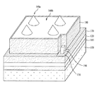
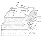
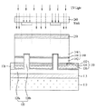
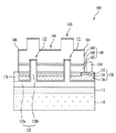
110 支持基板
115 接合層
120 第1の電極層
120a 主電極
120b 接触電極
130 第2の電極層
132 オーミック層
134 反射層
136 電流拡散層
140 発光構造物
142 第2の導電型半導体層
144 活性層
146 第1の導電型半導体層
148 凹凸構造
148a 凸部
148b 凹部
170 絶縁層
180 パッシベーション層
190 電極パッド
212、214 ビアホール
250 PR層
310 パッケージ本体
321、322 第1及び第2のリードフレーム
330 ワイヤ
340 モールディング部
350 蛍光体
400 ハウジング
500 放熱部
600 光源
700 ホルダー
710 発光モジュール
720 リフレクタ
730 シェード
800 表示装置
810 ボトムカバー
820 反射板
840 導光板
850 第1のプリズムシート
860 第2のプリズムシート
870 パネル
880 カラーフィルター
Claims (16)
- 第1の導電型半導体層、活性層及び第2の導電型半導体層を有する発光構造物と、
前記発光構造物の下部に位置し、前記第2の導電型半導体層と電気的に連結された第2の電極層と、
前記第2の電極層の下部に位置する主電極、及び前記主電極から分岐され、前記第2の電極層、前記第2の導電型半導体層及び前記活性層を貫通して前記第1の導電型半導体層と接する少なくとも1つの接触電極を有する第1の電極層と、
前記第1の電極層と前記第2の電極層との間及び第1の電極層と前記発光構造物との間の絶縁層と
を備え、
前記第1の導電型半導体層は、
第1の領域と、
前記第1の領域と区分され、前記第1の領域より低い第2の領域とを有し、
前記第1の領域は前記接触電極と重畳され、
前記接触電極の表面から前記第1の領域の前記第1の導電型半導体層の表面までの距離は、前記活性層から前記第2の領域の前記第1の導電型半導体層の表面までの距離より大きい、発光素子。 - 前記第1の領域の幅が前記接触電極の幅と同じか、前記接触電極の幅より広い、請求項1に記載の発光素子。
- 前記第1の領域の幅は前記接触電極の幅の1〜5倍である、請求項1又は2に記載の発光素子。
- 前記第1の導電型半導体層の上面にラフネス又はパターンが形成された、請求項1から請求項3のいずれか1項に記載の発光素子。
- 前記ラフネス又はパターンは前記第1の領域の側面に配置される、請求項4に記載の発光素子。
- 前記発光構造物の側面には、前記第2の導電型半導体層、前記活性層及び前記第1の導電型半導体層の少なくとも一部を覆うパッシベーション層をさらに備える、請求項1から請求項5のいずれか1項に記載の発光素子。
- 前記第2の電極層の一側が前記発光構造物の外部に露出し、露出した部分に電極パッドが形成されている、請求項1から請求項6のいずれか1項に記載の発光素子。
- 前記第2の電極層は、前記第2の導電型半導体層の下部に位置するオーミック層及び/又は反射層を有する、請求項1から請求項7のいずれか1項に記載の発光素子。
- 前記第2の電極層は電流拡散層を有し、前記電極パッドが前記電流拡散層と接して配置されている、請求項1から請求項8のいずれか1項に記載の発光素子。
- 前記第1の領域の形状は、ストライプ状、円柱状、円錐状、ピラミッド状、四角柱状又は半円球状のうちの少なくとも1つを含む、請求項1から請求項9のいずれか1項に記載の発光素子。
- 前記第1の導電型半導体層と接する前記接触電極の部分にラフネスが形成されている、請求項1から請求項10のいずれか1項に記載の発光素子。
- 前記第1の領域は前記接触電極と直接コンタクトする、請求項1から請求項11のいずれか1項に記載の発光素子。
- 前記第1の領域の上部面は、前記第2の領域の上部面より高い、請求項1から請求項12のいずれか1項に記載の発光素子。
- 前記第1の領域の上部面と前記活性層との間の距離は、前記第2の領域の上部面と前記活性層との間の距離より大きい、請求項1から請求項13のいずれか1項に記載の発光素子。
- 前記第1の領域は、前記接触電極の垂直上部に配置される、請求項1から請求項14のいずれか1項に記載の発光素子。
- 基板上に複数の発光素子パッケージを含んで光を放出する光源と、
前記光源が内蔵されたハウジングと、
前記光源の熱を放出する放熱部と、
前記光源と前記放熱部を前記ハウジングに結合するホルダーと
を備え、
前記発光素子パッケージは、
本体と、
前記本体に配置された第1及び第2のリードフレームと、
前記本体に配置され、前記第1及び第2のリードフレームと電気的に連結されている、請求項1から請求項15のいずれか1項に記載の発光素子とを備える照明装置。
Applications Claiming Priority (2)
| Application Number | Priority Date | Filing Date | Title |
|---|---|---|---|
| KR1020110102836A KR101827975B1 (ko) | 2011-10-10 | 2011-10-10 | 발광소자 |
| KR10-2011-0102836 | 2011-10-10 |
Publications (3)
| Publication Number | Publication Date |
|---|---|
| JP2013084878A JP2013084878A (ja) | 2013-05-09 |
| JP2013084878A5 JP2013084878A5 (ja) | 2015-03-19 |
| JP5923329B2 true JP5923329B2 (ja) | 2016-05-24 |
Family
ID=45936981
Family Applications (1)
| Application Number | Title | Priority Date | Filing Date |
|---|---|---|---|
| JP2012029681A Active JP5923329B2 (ja) | 2011-10-10 | 2012-02-14 | 発光素子及びこれを含む照明装置 |
Country Status (5)
| Country | Link |
|---|---|
| US (2) | US8884312B2 (ja) |
| EP (1) | EP2581952A3 (ja) |
| JP (1) | JP5923329B2 (ja) |
| KR (1) | KR101827975B1 (ja) |
| CN (1) | CN103035803B (ja) |
Families Citing this family (21)
| Publication number | Priority date | Publication date | Assignee | Title |
|---|---|---|---|---|
| CN103633232B (zh) * | 2012-08-22 | 2016-09-07 | 华夏光股份有限公司 | 半导体发光装置 |
| JP6519673B2 (ja) * | 2013-02-28 | 2019-05-29 | 日亜化学工業株式会社 | 半導体発光素子 |
| JP6287317B2 (ja) | 2013-02-28 | 2018-03-07 | 日亜化学工業株式会社 | 半導体発光素子 |
| DE102013107531A1 (de) * | 2013-07-16 | 2015-01-22 | Osram Opto Semiconductors Gmbh | Optoelektronischer Halbleiterchip |
| JP6302303B2 (ja) * | 2014-03-17 | 2018-03-28 | 株式会社東芝 | 半導体発光素子 |
| US10326050B2 (en) * | 2015-02-16 | 2019-06-18 | Seoul Viosys Co., Ltd. | Light-emitting device with improved light extraction efficiency |
| KR102343497B1 (ko) * | 2015-03-26 | 2021-12-27 | 쑤저우 레킨 세미컨덕터 컴퍼니 리미티드 | 발광 소자 및 이를 포함하는 발광 소자 패키지 |
| JP6563703B2 (ja) * | 2015-06-18 | 2019-08-21 | アルパッド株式会社 | 半導体発光装置 |
| DE102015111046B9 (de) * | 2015-07-08 | 2022-09-22 | OSRAM Opto Semiconductors Gesellschaft mit beschränkter Haftung | Optoelektronischer Halbleiterchip |
| KR102412409B1 (ko) * | 2015-10-26 | 2022-06-23 | 엘지전자 주식회사 | 반도체 발광 소자를 이용한 디스플레이 장치 및 이의 제조방법 |
| TWI646680B (zh) * | 2017-01-10 | 2019-01-01 | 英屬開曼群島商錼創科技股份有限公司 | 微型發光二極體晶片以及顯示面板 |
| US20210280741A1 (en) * | 2017-01-10 | 2021-09-09 | PlayNitride Inc. | Micro light emitting diode display panel |
| CN107293535B (zh) * | 2017-06-09 | 2020-01-10 | 电子科技大学 | 一种基于倒装封装的led芯片结构 |
| KR102410809B1 (ko) * | 2017-08-25 | 2022-06-20 | 쑤저우 레킨 세미컨덕터 컴퍼니 리미티드 | 반도체 소자 |
| JP7096489B2 (ja) * | 2018-09-20 | 2022-07-06 | 日亜化学工業株式会社 | 半導体素子の製造方法 |
| US20210074880A1 (en) * | 2018-12-18 | 2021-03-11 | Bolb Inc. | Light-output-power self-awareness light-emitting device |
| CN109713089A (zh) * | 2018-12-28 | 2019-05-03 | 映瑞光电科技(上海)有限公司 | GaN基LED白光垂直结构芯片及其制备方法 |
| CN111816783B (zh) * | 2019-04-12 | 2023-08-15 | 交互数字Ce专利控股公司 | 包括一组正圆形中空柱体的有机发光二极管单元 |
| CN110176438B (zh) * | 2019-06-11 | 2021-06-08 | 厦门市三安光电科技有限公司 | 发光二极管 |
| EP3944344B1 (en) | 2020-07-21 | 2022-10-19 | Nichia Corporation | Light emitting element and method of manufacturing light emitting element |
| JP7312953B2 (ja) * | 2020-07-21 | 2023-07-24 | 日亜化学工業株式会社 | 発光素子及び発光素子の製造方法 |
Family Cites Families (24)
| Publication number | Priority date | Publication date | Assignee | Title |
|---|---|---|---|---|
| DE60045092D1 (de) | 1999-03-29 | 2010-11-25 | Cambridge Display Tech Ltd | Zusammensetzung mit einem organischen elektrolumineszierenden Material |
| KR101221067B1 (ko) * | 2006-02-09 | 2013-01-11 | 삼성전자주식회사 | 리지 도파형 반도체 레이저 다이오드 |
| JP4835377B2 (ja) * | 2006-10-20 | 2011-12-14 | 日立電線株式会社 | 半導体発光素子 |
| TWI322522B (en) * | 2006-12-18 | 2010-03-21 | Delta Electronics Inc | Electroluminescent device, and fabrication method thereof |
| DE102007022947B4 (de) * | 2007-04-26 | 2022-05-05 | OSRAM Opto Semiconductors Gesellschaft mit beschränkter Haftung | Optoelektronischer Halbleiterkörper und Verfahren zur Herstellung eines solchen |
| TWI419355B (zh) * | 2007-09-21 | 2013-12-11 | Nat Univ Chung Hsing | 高光取出率的發光二極體晶片及其製造方法 |
| KR101164663B1 (ko) * | 2007-12-28 | 2012-07-12 | 니치아 카가쿠 고교 가부시키가이샤 | 반도체 발광 소자 및 그 제조방법 |
| DE102008022942A1 (de) * | 2008-05-09 | 2009-11-12 | Osram Opto Semiconductors Gmbh | Strahlungsemittierender Halbleiterchip |
| DE102008030584A1 (de) * | 2008-06-27 | 2009-12-31 | Osram Opto Semiconductors Gmbh | Verfahren zur Herstellung eines optoelektronischen Bauelementes und optoelektronisches Bauelement |
| JP5105310B2 (ja) * | 2008-08-19 | 2012-12-26 | 信越半導体株式会社 | 発光素子及びその製造方法 |
| US20110260192A1 (en) * | 2008-10-01 | 2011-10-27 | Chang Hoon Kwak | Light-emitting diode package using a liquid crystal polymer |
| KR101064016B1 (ko) * | 2008-11-26 | 2011-09-08 | 엘지이노텍 주식회사 | 발광 소자 및 그 제조방법 |
| JP5077224B2 (ja) * | 2008-12-26 | 2012-11-21 | 豊田合成株式会社 | Iii族窒化物半導体発光素子、およびその製造方法 |
| KR100974776B1 (ko) * | 2009-02-10 | 2010-08-06 | 엘지이노텍 주식회사 | 발광 소자 |
| KR101064053B1 (ko) * | 2009-02-25 | 2011-09-08 | 엘지이노텍 주식회사 | 발광소자 및 그 제조방법 |
| KR101020992B1 (ko) * | 2009-03-02 | 2011-03-09 | 엘지이노텍 주식회사 | 발광 모듈 및 이를 구비한 라이트 유닛 |
| KR20110008550A (ko) * | 2009-07-20 | 2011-01-27 | 삼성전자주식회사 | 발광 소자 및 그 제조 방법 |
| US8115369B2 (en) * | 2009-11-09 | 2012-02-14 | Lg Innotek Co., Ltd. | Lighting device |
| DE102009060274A1 (de) | 2009-12-23 | 2011-06-30 | DeguDent GmbH, 63457 | Lithiumdisilikat-Glaskeramik, Verfahren zu deren Herstellung und deren Verwendung |
| KR100986560B1 (ko) | 2010-02-11 | 2010-10-07 | 엘지이노텍 주식회사 | 발광소자 및 그 제조방법 |
| JP5733594B2 (ja) * | 2010-02-18 | 2015-06-10 | スタンレー電気株式会社 | 半導体発光装置 |
| KR101761385B1 (ko) * | 2010-07-12 | 2017-08-04 | 엘지이노텍 주식회사 | 발광 소자 |
| EP2442374B1 (en) * | 2010-10-12 | 2016-09-21 | LG Innotek Co., Ltd. | Light emitting device |
| KR101860973B1 (ko) | 2011-05-25 | 2018-05-24 | 오스람 옵토 세미컨덕터스 게엠베하 | 광전 반도체 칩 |
-
2011
- 2011-10-10 KR KR1020110102836A patent/KR101827975B1/ko active IP Right Grant
-
2012
- 2012-02-10 US US13/370,601 patent/US8884312B2/en active Active
- 2012-02-14 JP JP2012029681A patent/JP5923329B2/ja active Active
- 2012-03-29 EP EP12162167.6A patent/EP2581952A3/en not_active Withdrawn
- 2012-05-29 CN CN201210171651.8A patent/CN103035803B/zh active Active
-
2014
- 2014-09-29 US US14/499,459 patent/US9356007B2/en active Active
Also Published As
| Publication number | Publication date |
|---|---|
| US20130087814A1 (en) | 2013-04-11 |
| KR20130038465A (ko) | 2013-04-18 |
| CN103035803B (zh) | 2017-05-31 |
| JP2013084878A (ja) | 2013-05-09 |
| CN103035803A (zh) | 2013-04-10 |
| US9356007B2 (en) | 2016-05-31 |
| EP2581952A2 (en) | 2013-04-17 |
| US8884312B2 (en) | 2014-11-11 |
| EP2581952A3 (en) | 2016-03-09 |
| US20150014713A1 (en) | 2015-01-15 |
| KR101827975B1 (ko) | 2018-03-29 |
Similar Documents
| Publication | Publication Date | Title |
|---|---|---|
| JP5923329B2 (ja) | 発光素子及びこれを含む照明装置 | |
| US8710535B2 (en) | Light emitting device and light emitting device package | |
| KR102197082B1 (ko) | 발광 소자 및 이를 포함하는 발광소자 패키지 | |
| US8575635B2 (en) | Light emitting device, light emitting device package, and lighting system | |
| JP6215554B2 (ja) | 発光素子 | |
| KR101799451B1 (ko) | 발광 소자 | |
| US20110220937A1 (en) | Light emitting device and ligth emitting device pakage | |
| US20110220946A1 (en) | Light emitting device, light emitting device package, and lighting system | |
| JP5971917B2 (ja) | 発光素子及び該発光素子を含む映像表示装置 | |
| JP2012028779A (ja) | 発光素子、これを含む発光素子パッケージ及び照明システム | |
| JP5999884B2 (ja) | 発光素子、発光素子パッケージ、及び照明装置 | |
| US8686456B2 (en) | Light emitting device, light emitting device package, and light unit | |
| KR101941029B1 (ko) | 발광소자 및 이를 포함하는 조명시스템 | |
| KR20110115384A (ko) | 발광 소자 및 그 제조방법, 발광 소자 패키지 및 조명 시스템 | |
| KR20170082889A (ko) | 발광소자 | |
| KR101974153B1 (ko) | 발광 소자 및 이를 포함하는 조명 시스템 | |
| KR101929933B1 (ko) | 발광 소자 및 이를 포함하는 조명 시스템 | |
| KR20120014972A (ko) | 발광 소자, 발광 소자 제조방법, 발광 소자 패키지, 및 조명 시스템 | |
| KR20130138416A (ko) | 발광소자 | |
| KR101729267B1 (ko) | 발광 소자 | |
| KR20130139018A (ko) | 발광 소자 | |
| KR20120050089A (ko) | 발광소자 및 그 제조방법 | |
| KR101911865B1 (ko) | 발광소자 | |
| KR101710889B1 (ko) | 발광 소자 | |
| KR20170082872A (ko) | 발광소자 |
Legal Events
| Date | Code | Title | Description |
|---|---|---|---|
| A521 | Request for written amendment filed |
Free format text: JAPANESE INTERMEDIATE CODE: A523 Effective date: 20150130 |
|
| A621 | Written request for application examination |
Free format text: JAPANESE INTERMEDIATE CODE: A621 Effective date: 20150130 |
|
| A977 | Report on retrieval |
Free format text: JAPANESE INTERMEDIATE CODE: A971007 Effective date: 20150925 |
|
| A131 | Notification of reasons for refusal |
Free format text: JAPANESE INTERMEDIATE CODE: A131 Effective date: 20151006 |
|
| A521 | Request for written amendment filed |
Free format text: JAPANESE INTERMEDIATE CODE: A523 Effective date: 20151208 |
|
| TRDD | Decision of grant or rejection written | ||
| A01 | Written decision to grant a patent or to grant a registration (utility model) |
Free format text: JAPANESE INTERMEDIATE CODE: A01 Effective date: 20160405 |
|
| A61 | First payment of annual fees (during grant procedure) |
Free format text: JAPANESE INTERMEDIATE CODE: A61 Effective date: 20160418 |
|
| R150 | Certificate of patent or registration of utility model |
Ref document number: 5923329 Country of ref document: JP Free format text: JAPANESE INTERMEDIATE CODE: R150 |
|
| R250 | Receipt of annual fees |
Free format text: JAPANESE INTERMEDIATE CODE: R250 |
|
| R250 | Receipt of annual fees |
Free format text: JAPANESE INTERMEDIATE CODE: R250 |
|
| R250 | Receipt of annual fees |
Free format text: JAPANESE INTERMEDIATE CODE: R250 |
|
| S531 | Written request for registration of change of domicile |
Free format text: JAPANESE INTERMEDIATE CODE: R313531 |
|
| S111 | Request for change of ownership or part of ownership |
Free format text: JAPANESE INTERMEDIATE CODE: R313113 |
|
| R350 | Written notification of registration of transfer |
Free format text: JAPANESE INTERMEDIATE CODE: R350 |
|
| R350 | Written notification of registration of transfer |
Free format text: JAPANESE INTERMEDIATE CODE: R350 |
|
| R250 | Receipt of annual fees |
Free format text: JAPANESE INTERMEDIATE CODE: R250 |
|
| R250 | Receipt of annual fees |
Free format text: JAPANESE INTERMEDIATE CODE: R250 |