JP5739824B2 - 非極性または半極性(Ga、Al、In、B)N基板上に成長させられる素子 - Google Patents
非極性または半極性(Ga、Al、In、B)N基板上に成長させられる素子 Download PDFInfo
- Publication number
- JP5739824B2 JP5739824B2 JP2011553052A JP2011553052A JP5739824B2 JP 5739824 B2 JP5739824 B2 JP 5739824B2 JP 2011553052 A JP2011553052 A JP 2011553052A JP 2011553052 A JP2011553052 A JP 2011553052A JP 5739824 B2 JP5739824 B2 JP 5739824B2
- Authority
- JP
- Japan
- Prior art keywords
- film
- substrate
- semipolar
- nonpolar
- plane
- Prior art date
- Legal status (The legal status is an assumption and is not a legal conclusion. Google has not performed a legal analysis and makes no representation as to the accuracy of the status listed.)
- Expired - Fee Related
Links
- 229910052796 boron Inorganic materials 0.000 title claims description 97
- 229910052738 indium Inorganic materials 0.000 title claims description 97
- 229910052733 gallium Inorganic materials 0.000 title claims description 96
- 229910052782 aluminium Inorganic materials 0.000 title claims description 95
- 239000000758 substrate Substances 0.000 title claims description 92
- JMASRVWKEDWRBT-UHFFFAOYSA-N Gallium nitride Chemical compound [Ga]#N JMASRVWKEDWRBT-UHFFFAOYSA-N 0.000 claims description 66
- 230000012010 growth Effects 0.000 claims description 66
- 229910002601 GaN Inorganic materials 0.000 claims description 62
- 150000004767 nitrides Chemical class 0.000 claims description 57
- 239000012159 carrier gas Substances 0.000 claims description 55
- 238000000034 method Methods 0.000 claims description 51
- 230000003746 surface roughness Effects 0.000 claims description 24
- 239000013078 crystal Substances 0.000 claims description 19
- 230000003287 optical effect Effects 0.000 claims description 18
- 239000012528 membrane Substances 0.000 claims description 17
- 239000011261 inert gas Substances 0.000 claims description 12
- 239000000203 mixture Substances 0.000 claims description 12
- 125000004433 nitrogen atom Chemical group N* 0.000 claims description 8
- 238000000151 deposition Methods 0.000 claims description 7
- 230000008021 deposition Effects 0.000 claims description 6
- 230000008569 process Effects 0.000 claims description 6
- 229910052786 argon Inorganic materials 0.000 claims description 5
- 229910052734 helium Inorganic materials 0.000 claims description 5
- 229910052754 neon Inorganic materials 0.000 claims description 5
- 238000012545 processing Methods 0.000 claims description 5
- 229910052743 krypton Inorganic materials 0.000 claims description 4
- 238000005229 chemical vapour deposition Methods 0.000 claims description 3
- 230000015572 biosynthetic process Effects 0.000 claims 1
- 239000010408 film Substances 0.000 description 60
- 239000010409 thin film Substances 0.000 description 48
- 230000010287 polarization Effects 0.000 description 21
- 230000000694 effects Effects 0.000 description 16
- 230000005684 electric field Effects 0.000 description 10
- 229910052984 zinc sulfide Inorganic materials 0.000 description 8
- 230000008901 benefit Effects 0.000 description 7
- 238000005401 electroluminescence Methods 0.000 description 7
- 229910052757 nitrogen Inorganic materials 0.000 description 7
- 230000006911 nucleation Effects 0.000 description 7
- 238000010899 nucleation Methods 0.000 description 7
- 235000019592 roughness Nutrition 0.000 description 7
- 238000010586 diagram Methods 0.000 description 6
- 238000000879 optical micrograph Methods 0.000 description 6
- 235000012431 wafers Nutrition 0.000 description 6
- 238000002248 hydride vapour-phase epitaxy Methods 0.000 description 5
- 230000009467 reduction Effects 0.000 description 5
- 229910052710 silicon Inorganic materials 0.000 description 4
- 239000007787 solid Substances 0.000 description 4
- 239000002019 doping agent Substances 0.000 description 3
- 230000006872 improvement Effects 0.000 description 3
- 238000004519 manufacturing process Methods 0.000 description 3
- 239000002243 precursor Substances 0.000 description 3
- 239000004065 semiconductor Substances 0.000 description 3
- 238000000926 separation method Methods 0.000 description 3
- QGZKDVFQNNGYKY-UHFFFAOYSA-N Ammonia Chemical compound N QGZKDVFQNNGYKY-UHFFFAOYSA-N 0.000 description 2
- XKRFYHLGVUSROY-UHFFFAOYSA-N Argon Chemical compound [Ar] XKRFYHLGVUSROY-UHFFFAOYSA-N 0.000 description 2
- 229910001218 Gallium arsenide Inorganic materials 0.000 description 2
- 241000921519 Syrrhopodon sp. Species 0.000 description 2
- XLOMVQKBTHCTTD-UHFFFAOYSA-N Zinc monoxide Chemical compound [Zn]=O XLOMVQKBTHCTTD-UHFFFAOYSA-N 0.000 description 2
- 230000002411 adverse Effects 0.000 description 2
- 229910045601 alloy Inorganic materials 0.000 description 2
- 239000000956 alloy Substances 0.000 description 2
- 238000013459 approach Methods 0.000 description 2
- 230000009286 beneficial effect Effects 0.000 description 2
- 239000000969 carrier Substances 0.000 description 2
- 238000005520 cutting process Methods 0.000 description 2
- 238000013500 data storage Methods 0.000 description 2
- 230000003247 decreasing effect Effects 0.000 description 2
- 229910052742 iron Inorganic materials 0.000 description 2
- 238000005259 measurement Methods 0.000 description 2
- 229910052751 metal Inorganic materials 0.000 description 2
- 239000002184 metal Substances 0.000 description 2
- 230000004048 modification Effects 0.000 description 2
- 238000012986 modification Methods 0.000 description 2
- 230000005693 optoelectronics Effects 0.000 description 2
- 230000005701 quantum confined stark effect Effects 0.000 description 2
- 229910052594 sapphire Inorganic materials 0.000 description 2
- 239000010980 sapphire Substances 0.000 description 2
- WGPCGCOKHWGKJJ-UHFFFAOYSA-N sulfanylidenezinc Chemical compound [Zn]=S WGPCGCOKHWGKJJ-UHFFFAOYSA-N 0.000 description 2
- 238000004381 surface treatment Methods 0.000 description 2
- XCZXGTMEAKBVPV-UHFFFAOYSA-N trimethylgallium Chemical compound C[Ga](C)C XCZXGTMEAKBVPV-UHFFFAOYSA-N 0.000 description 2
- 238000000927 vapour-phase epitaxy Methods 0.000 description 2
- 230000005428 wave function Effects 0.000 description 2
- 229910052725 zinc Inorganic materials 0.000 description 2
- 239000011701 zinc Substances 0.000 description 2
- 229910002704 AlGaN Inorganic materials 0.000 description 1
- IJGRMHOSHXDMSA-UHFFFAOYSA-N Atomic nitrogen Chemical compound N#N IJGRMHOSHXDMSA-UHFFFAOYSA-N 0.000 description 1
- 229910052582 BN Inorganic materials 0.000 description 1
- PZNSFCLAULLKQX-UHFFFAOYSA-N Boron nitride Chemical compound N#B PZNSFCLAULLKQX-UHFFFAOYSA-N 0.000 description 1
- 240000001973 Ficus microcarpa Species 0.000 description 1
- GYHNNYVSQQEPJS-UHFFFAOYSA-N Gallium Chemical compound [Ga] GYHNNYVSQQEPJS-UHFFFAOYSA-N 0.000 description 1
- 229910010093 LiAlO Inorganic materials 0.000 description 1
- 229910001199 N alloy Inorganic materials 0.000 description 1
- BLRPTPMANUNPDV-UHFFFAOYSA-N Silane Chemical compound [SiH4] BLRPTPMANUNPDV-UHFFFAOYSA-N 0.000 description 1
- XUIMIQQOPSSXEZ-UHFFFAOYSA-N Silicon Chemical compound [Si] XUIMIQQOPSSXEZ-UHFFFAOYSA-N 0.000 description 1
- 238000009825 accumulation Methods 0.000 description 1
- 229910021529 ammonia Inorganic materials 0.000 description 1
- 238000000149 argon plasma sintering Methods 0.000 description 1
- 230000004888 barrier function Effects 0.000 description 1
- 238000005452 bending Methods 0.000 description 1
- 230000000903 blocking effect Effects 0.000 description 1
- 238000004364 calculation method Methods 0.000 description 1
- 238000004140 cleaning Methods 0.000 description 1
- PMHQVHHXPFUNSP-UHFFFAOYSA-M copper(1+);methylsulfanylmethane;bromide Chemical compound Br[Cu].CSC PMHQVHHXPFUNSP-UHFFFAOYSA-M 0.000 description 1
- RKTYLMNFRDHKIL-UHFFFAOYSA-N copper;5,10,15,20-tetraphenylporphyrin-22,24-diide Chemical group [Cu+2].C1=CC(C(=C2C=CC([N-]2)=C(C=2C=CC=CC=2)C=2C=CC(N=2)=C(C=2C=CC=CC=2)C2=CC=C3[N-]2)C=2C=CC=CC=2)=NC1=C3C1=CC=CC=C1 RKTYLMNFRDHKIL-UHFFFAOYSA-N 0.000 description 1
- 230000008878 coupling Effects 0.000 description 1
- 238000010168 coupling process Methods 0.000 description 1
- 238000005859 coupling reaction Methods 0.000 description 1
- 238000002109 crystal growth method Methods 0.000 description 1
- 238000013461 design Methods 0.000 description 1
- 239000010432 diamond Substances 0.000 description 1
- 238000001194 electroluminescence spectrum Methods 0.000 description 1
- 238000005516 engineering process Methods 0.000 description 1
- 238000000605 extraction Methods 0.000 description 1
- 239000007789 gas Substances 0.000 description 1
- 229910052732 germanium Inorganic materials 0.000 description 1
- GNPVGFCGXDBREM-UHFFFAOYSA-N germanium atom Chemical compound [Ge] GNPVGFCGXDBREM-UHFFFAOYSA-N 0.000 description 1
- 238000010438 heat treatment Methods 0.000 description 1
- 239000001307 helium Substances 0.000 description 1
- SWQJXJOGLNCZEY-UHFFFAOYSA-N helium atom Chemical compound [He] SWQJXJOGLNCZEY-UHFFFAOYSA-N 0.000 description 1
- 239000012535 impurity Substances 0.000 description 1
- 238000002347 injection Methods 0.000 description 1
- 239000007924 injection Substances 0.000 description 1
- DNNSSWSSYDEUBZ-UHFFFAOYSA-N krypton atom Chemical compound [Kr] DNNSSWSSYDEUBZ-UHFFFAOYSA-N 0.000 description 1
- YQNQTEBHHUSESQ-UHFFFAOYSA-N lithium aluminate Chemical compound [Li+].[O-][Al]=O YQNQTEBHHUSESQ-UHFFFAOYSA-N 0.000 description 1
- GQYHUHYESMUTHG-UHFFFAOYSA-N lithium niobate Chemical compound [Li+].[O-][Nb](=O)=O GQYHUHYESMUTHG-UHFFFAOYSA-N 0.000 description 1
- MNKMDLVKGZBOEW-UHFFFAOYSA-M lithium;3,4,5-trihydroxybenzoate Chemical compound [Li+].OC1=CC(C([O-])=O)=CC(O)=C1O MNKMDLVKGZBOEW-UHFFFAOYSA-M 0.000 description 1
- 229910052749 magnesium Inorganic materials 0.000 description 1
- 239000000463 material Substances 0.000 description 1
- 239000011159 matrix material Substances 0.000 description 1
- 238000001000 micrograph Methods 0.000 description 1
- 238000001451 molecular beam epitaxy Methods 0.000 description 1
- GKAOGPIIYCISHV-UHFFFAOYSA-N neon atom Chemical compound [Ne] GKAOGPIIYCISHV-UHFFFAOYSA-N 0.000 description 1
- 230000007935 neutral effect Effects 0.000 description 1
- 238000005457 optimization Methods 0.000 description 1
- 238000005498 polishing Methods 0.000 description 1
- 238000003908 quality control method Methods 0.000 description 1
- 230000005855 radiation Effects 0.000 description 1
- 239000002994 raw material Substances 0.000 description 1
- 229910000077 silane Inorganic materials 0.000 description 1
- 239000010703 silicon Substances 0.000 description 1
- HBMJWWWQQXIZIP-UHFFFAOYSA-N silicon carbide Chemical compound [Si+]#[C-] HBMJWWWQQXIZIP-UHFFFAOYSA-N 0.000 description 1
- 229910010271 silicon carbide Inorganic materials 0.000 description 1
- 239000010454 slate Substances 0.000 description 1
- 239000011029 spinel Substances 0.000 description 1
- 229910052596 spinel Inorganic materials 0.000 description 1
- 230000002269 spontaneous effect Effects 0.000 description 1
- 239000000126 substance Substances 0.000 description 1
- 230000007704 transition Effects 0.000 description 1
- 238000007740 vapor deposition Methods 0.000 description 1
- 229910052724 xenon Inorganic materials 0.000 description 1
- FHNFHKCVQCLJFQ-UHFFFAOYSA-N xenon atom Chemical compound [Xe] FHNFHKCVQCLJFQ-UHFFFAOYSA-N 0.000 description 1
- 239000011787 zinc oxide Substances 0.000 description 1
Images


Classifications
-
- H—ELECTRICITY
- H01—ELECTRIC ELEMENTS
- H01L—SEMICONDUCTOR DEVICES NOT COVERED BY CLASS H10
- H01L21/00—Processes or apparatus adapted for the manufacture or treatment of semiconductor or solid state devices or of parts thereof
- H01L21/02—Manufacture or treatment of semiconductor devices or of parts thereof
- H01L21/02104—Forming layers
- H01L21/02365—Forming inorganic semiconducting materials on a substrate
- H01L21/02518—Deposited layers
- H01L21/02609—Crystal orientation
-
- H—ELECTRICITY
- H01—ELECTRIC ELEMENTS
- H01L—SEMICONDUCTOR DEVICES NOT COVERED BY CLASS H10
- H01L21/00—Processes or apparatus adapted for the manufacture or treatment of semiconductor or solid state devices or of parts thereof
- H01L21/02—Manufacture or treatment of semiconductor devices or of parts thereof
- H01L21/02104—Forming layers
- H01L21/02365—Forming inorganic semiconducting materials on a substrate
- H01L21/02367—Substrates
- H01L21/0237—Materials
- H01L21/02387—Group 13/15 materials
- H01L21/02389—Nitrides
-
- H—ELECTRICITY
- H01—ELECTRIC ELEMENTS
- H01L—SEMICONDUCTOR DEVICES NOT COVERED BY CLASS H10
- H01L21/00—Processes or apparatus adapted for the manufacture or treatment of semiconductor or solid state devices or of parts thereof
- H01L21/02—Manufacture or treatment of semiconductor devices or of parts thereof
- H01L21/04—Manufacture or treatment of semiconductor devices or of parts thereof the devices having potential barriers, e.g. a PN junction, depletion layer or carrier concentration layer
- H01L21/18—Manufacture or treatment of semiconductor devices or of parts thereof the devices having potential barriers, e.g. a PN junction, depletion layer or carrier concentration layer the devices having semiconductor bodies comprising elements of Group IV of the Periodic Table or AIIIBV compounds with or without impurities, e.g. doping materials
- H01L21/20—Deposition of semiconductor materials on a substrate, e.g. epitaxial growth solid phase epitaxy
-
- H—ELECTRICITY
- H01—ELECTRIC ELEMENTS
- H01L—SEMICONDUCTOR DEVICES NOT COVERED BY CLASS H10
- H01L21/00—Processes or apparatus adapted for the manufacture or treatment of semiconductor or solid state devices or of parts thereof
- H01L21/02—Manufacture or treatment of semiconductor devices or of parts thereof
- H01L21/02104—Forming layers
- H01L21/02365—Forming inorganic semiconducting materials on a substrate
- H01L21/02367—Substrates
- H01L21/02433—Crystal orientation
-
- H—ELECTRICITY
- H01—ELECTRIC ELEMENTS
- H01L—SEMICONDUCTOR DEVICES NOT COVERED BY CLASS H10
- H01L21/00—Processes or apparatus adapted for the manufacture or treatment of semiconductor or solid state devices or of parts thereof
- H01L21/02—Manufacture or treatment of semiconductor devices or of parts thereof
- H01L21/02104—Forming layers
- H01L21/02365—Forming inorganic semiconducting materials on a substrate
- H01L21/02518—Deposited layers
- H01L21/02521—Materials
- H01L21/02538—Group 13/15 materials
- H01L21/0254—Nitrides
-
- H—ELECTRICITY
- H01—ELECTRIC ELEMENTS
- H01L—SEMICONDUCTOR DEVICES NOT COVERED BY CLASS H10
- H01L21/00—Processes or apparatus adapted for the manufacture or treatment of semiconductor or solid state devices or of parts thereof
- H01L21/02—Manufacture or treatment of semiconductor devices or of parts thereof
- H01L21/02104—Forming layers
- H01L21/02365—Forming inorganic semiconducting materials on a substrate
- H01L21/02612—Formation types
- H01L21/02617—Deposition types
- H01L21/0262—Reduction or decomposition of gaseous compounds, e.g. CVD
-
- H—ELECTRICITY
- H01—ELECTRIC ELEMENTS
- H01L—SEMICONDUCTOR DEVICES NOT COVERED BY CLASS H10
- H01L33/00—Semiconductor devices having potential barriers specially adapted for light emission; Processes or apparatus specially adapted for the manufacture or treatment thereof or of parts thereof; Details thereof
- H01L33/005—Processes
- H01L33/0062—Processes for devices with an active region comprising only III-V compounds
- H01L33/0066—Processes for devices with an active region comprising only III-V compounds with a substrate not being a III-V compound
- H01L33/007—Processes for devices with an active region comprising only III-V compounds with a substrate not being a III-V compound comprising nitride compounds
-
- H—ELECTRICITY
- H01—ELECTRIC ELEMENTS
- H01L—SEMICONDUCTOR DEVICES NOT COVERED BY CLASS H10
- H01L33/00—Semiconductor devices having potential barriers specially adapted for light emission; Processes or apparatus specially adapted for the manufacture or treatment thereof or of parts thereof; Details thereof
- H01L33/02—Semiconductor devices having potential barriers specially adapted for light emission; Processes or apparatus specially adapted for the manufacture or treatment thereof or of parts thereof; Details thereof characterised by the semiconductor bodies
- H01L33/26—Materials of the light emitting region
- H01L33/30—Materials of the light emitting region containing only elements of Group III and Group V of the Periodic Table
- H01L33/32—Materials of the light emitting region containing only elements of Group III and Group V of the Periodic Table containing nitrogen
-
- H—ELECTRICITY
- H01—ELECTRIC ELEMENTS
- H01S—DEVICES USING THE PROCESS OF LIGHT AMPLIFICATION BY STIMULATED EMISSION OF RADIATION [LASER] TO AMPLIFY OR GENERATE LIGHT; DEVICES USING STIMULATED EMISSION OF ELECTROMAGNETIC RADIATION IN WAVE RANGES OTHER THAN OPTICAL
- H01S5/00—Semiconductor lasers
- H01S5/30—Structure or shape of the active region; Materials used for the active region
- H01S5/34—Structure or shape of the active region; Materials used for the active region comprising quantum well or superlattice structures, e.g. single quantum well [SQW] lasers, multiple quantum well [MQW] lasers or graded index separate confinement heterostructure [GRINSCH] lasers
- H01S5/343—Structure or shape of the active region; Materials used for the active region comprising quantum well or superlattice structures, e.g. single quantum well [SQW] lasers, multiple quantum well [MQW] lasers or graded index separate confinement heterostructure [GRINSCH] lasers in AIIIBV compounds, e.g. AlGaAs-laser, InP-based laser
-
- H—ELECTRICITY
- H01—ELECTRIC ELEMENTS
- H01L—SEMICONDUCTOR DEVICES NOT COVERED BY CLASS H10
- H01L33/00—Semiconductor devices having potential barriers specially adapted for light emission; Processes or apparatus specially adapted for the manufacture or treatment thereof or of parts thereof; Details thereof
- H01L33/02—Semiconductor devices having potential barriers specially adapted for light emission; Processes or apparatus specially adapted for the manufacture or treatment thereof or of parts thereof; Details thereof characterised by the semiconductor bodies
- H01L33/16—Semiconductor devices having potential barriers specially adapted for light emission; Processes or apparatus specially adapted for the manufacture or treatment thereof or of parts thereof; Details thereof characterised by the semiconductor bodies with a particular crystal structure or orientation, e.g. polycrystalline, amorphous or porous
- H01L33/18—Semiconductor devices having potential barriers specially adapted for light emission; Processes or apparatus specially adapted for the manufacture or treatment thereof or of parts thereof; Details thereof characterised by the semiconductor bodies with a particular crystal structure or orientation, e.g. polycrystalline, amorphous or porous within the light emitting region
-
- Y—GENERAL TAGGING OF NEW TECHNOLOGICAL DEVELOPMENTS; GENERAL TAGGING OF CROSS-SECTIONAL TECHNOLOGIES SPANNING OVER SEVERAL SECTIONS OF THE IPC; TECHNICAL SUBJECTS COVERED BY FORMER USPC CROSS-REFERENCE ART COLLECTIONS [XRACs] AND DIGESTS
- Y10—TECHNICAL SUBJECTS COVERED BY FORMER USPC
- Y10T—TECHNICAL SUBJECTS COVERED BY FORMER US CLASSIFICATION
- Y10T428/00—Stock material or miscellaneous articles
- Y10T428/31—Surface property or characteristic of web, sheet or block
Landscapes
- Engineering & Computer Science (AREA)
- Manufacturing & Machinery (AREA)
- Power Engineering (AREA)
- Microelectronics & Electronic Packaging (AREA)
- Computer Hardware Design (AREA)
- Physics & Mathematics (AREA)
- Condensed Matter Physics & Semiconductors (AREA)
- General Physics & Mathematics (AREA)
- Chemical & Material Sciences (AREA)
- Crystallography & Structural Chemistry (AREA)
- Materials Engineering (AREA)
- Electromagnetism (AREA)
- Optics & Photonics (AREA)
- Led Devices (AREA)
- Semiconductor Lasers (AREA)
- Recrystallisation Techniques (AREA)
- Crystals, And After-Treatments Of Crystals (AREA)
Description
本願は、同時係属で共通譲受人の下記の出願;
Robert M.Farrell、Michael Iza、James S.Speck、Steven P.DenBaars、およびShuji Nakamuraによる米国仮特許出願第61/156,710号(名称「METHOD OF IMPROVING SURFACE MORPHOLOGY OF (Ga,Al,In,B)N THIN FILMS AND DEVICES GROWN ON NONPOLAR OR SEMIPOLAR (Ga,Al,In,B)N SUBSTRATES」、2009年3月2日出願、代理人整理番号第30794.306−US−P1(2009−429−1)号);および
Robert M.Farrell、Michael Iza、James S.Speck、Steven P.DenBaars、およびShuji Nakamuraによる米国仮特許出願第61/184,535号(名称「METHOD OF IMPROVING SURFACE MORPHOLOGY OF (Ga,Al,In,B)N THIN FILMS AND DEVICES GROWN ON NONPOLAR OR SEMIPOLAR (Ga,Al,In,B)N SUBSTRATES」、2009年6月5日出願、代理人整理番号第0794.306−US−P2 (2009−429−2)号);
の米国特許法第119条第(e)項の利益を主張し、これらの出願は、本明細書に参考として援用される。
本発明は、半導体材料、方法、および素子に関し、より具体的には、非極性または半極性の窒化物発光ダイオード(LED)およびダイオードレーザの成長に関する。
(注:本願は、明細書の全体を通して示されるように、角括弧内の1つ以上の参照番号、例えば[Ref(s).x]によって多数の異なる刊行物を参照する。これらの参照番号による順序で示されるこれらの異なる刊行物の一覧は、以下の「参考文献」という表題の項に見出すことができる。これらの刊行物のそれぞれは、参照することによって本明細書に組み込まれる。)
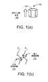
窒化ガリウム(GaN)および(Ga、Al、In、B)N合金の有用性は、可視光および紫外線光電子素子ならびに高出力電子素子の加工に対して確立されている。最先端の窒化物薄膜、ヘテロ構造、および素子は、[0001]軸に沿って成長させられる。そのような膜の全分極は、自発および圧電分極寄与から構成され、その両方とも、図1(a)に例示されるように、ウルツ鉱窒化物結晶構造102の単極性[0001]軸100から生じる。窒化物ヘテロ構造が、疑似形態的に成長させられる場合、分極断絶が、表面(例えば、図1(a)に示される、c−面表面104)および結晶102内の界面に形成される。これらの断絶は、表面および界面におけるキャリアの蓄積または枯渇につながり、順に、電場を引き起こす。これらの分極誘導電場の方位は、窒化物薄膜およびヘテロ構造の典型的[0001]成長方向と一致するため、これらの場は、窒化物素子のエネルギーバンドを「傾動」させる効果を有する。
本発明は、例えば、以下の項目も提供する。
(項目1)
(Ga、Al、In、B)N薄膜を加工する方法であって、
(Ga、Al、In、B)N膜を非極性または半極性の(Ga、Al、In、B)N基板もしくはテンプレート上に直接成長させることと、
該成長ステップの間、キャリアガスを使用することであって、該キャリアガスの少なくとも一部は不活性ガスから構成される、ことと
を含む、方法。
(項目2)
前記基板またはテンプレートに、低指数の結晶方位から離れる方向のミスカットを提供することをさらに含む、項目1に記載の方法。
(項目3)
前記基板あるいはテンプレートは、m−面の基板あるいはテンプレートであって、前記ミスカットは、[000−1]方向に向かい、0.75°乃至1.50°のミスカット角度を有し、(Ga、Al、In、B)N膜は、該ミスカットの表面上に成長させられる、項目2に記載の方法。
(項目4)
前記不活性ガスは、N 2 、He、Ne、Ar、Kr、またはXeのうちの1つ以上から構成される、項目1に記載の方法。
(項目5)
1つ以上の素子層が、前記膜の上面に配置され、該素子層は、H 2 から構成され、前記キャリアガスの少なくとも一部によって成長させられる、項目1に記載の方法。
(項目6)
前記素子層は、前記素子の1つ以上のp型ドープ層を含み、該p型ドープ層は、H 2 から構成されている前記キャリアガスの少なくとも一部によって成長させられる、項目5に記載の方法。
(項目7)
非極性または半極性の(Ga、Al、In、B)Nの膜であって、
非極性または半極性の面である上面であって、該上面は、平面で光学的に平滑な領域を有することにより、該領域が、光学顕微鏡を使用して、400ナノメートル乃至600ナノメートルの光波長を用いて測定される場合、識別可能な非平面の表面起伏または特徴が無い、上面を備えており、該領域は、20ミリアンペアの駆動電流において少なくとも2ミリワットの出力強度を有する光を発する1つ以上の素子層のエピタキシャル析出のための基板としての使用に対して十分に大きい、膜。
(項目8)
前記領域は、ストライエーションが無い、項目7に記載の膜。
(項目9)
前記領域は、少なくとも100平方マイクロメートルである、項目7に記載の膜。
(項目10)
前記上面は、Ga、Al、In、B、およびNの原子の直径のオーダーの表面粗度を有して原子的に平滑である、項目9に記載の膜。
(項目11)
前記上面は、前記領域にわたって、0.5ナノメートル未満の二乗平均を有する表面粗度を有する、項目9に記載の膜。
(項目12)
前記上面は、前記領域にわたって、0.25ナノメートル未満の二乗平均を有する表面粗度を有する、項目9に記載の膜。
(項目13)
前記膜は、m−面基板の表面上に析出され、該m−面基板の表面は、[000−1]方向に向かい、0.75°乃至1.50°のミスカット角度を有するミスカットである、項目9に記載の膜。
(項目14)
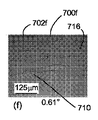
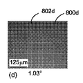
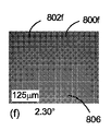
前記上面の領域は、図2(a)−2(b)、3(a)−3(f)、4(a)−4(b)、5、6(a)−6(b)、7(a)−7(c)、8(a)−8(c)、または9(d)−9(f)に示される上面よりも平滑かつ平面である、項目7に記載の膜。
(項目15)
前記上面の領域は、密度8.4×10 2 cm −2 、大きさ10マイクロメートル、および勾配角度0.1°を有するピラミッド形小丘で特徴付けられた表面よりも平滑である、項目7に記載の膜。
(項目16)
前記上面の領域は、密度1.1×10 6 cm −2 を有する、ピラミッド形小丘で特徴付けられた表面よりも平滑である、項目7に記載の膜。
(項目17)
前記上面は、図7(d)−7(f)、8(d)−8(f)、または9(a)−9(c)に示される表面と少なくとも同程度に平滑である平滑度または表面粗度を有する、項目7に記載の膜。
(項目18)
前記膜は、m−面GaN膜であって、前記上面は、該m−面GaN膜のm−面である、項目7に記載の膜。
(項目19)
前記素子層は、前記膜の上面と少なくとも同程度に平滑である上面を有する、項目7に記載の膜。
(項目20)
前記上面の表面の平滑度または粗度は、成長した状態のままである、項目7に記載の膜。
非極性または半極性の窒化物LEDおよびダイオードレーザの実現は、窒化物LEDおよびダイオードレーザの製造可能性における多数の進歩を可能にする。非極性または半極性面上での窒化物LEDおよびダイオードレーザの成長は、重正孔および軽正孔バンドの異方性歪み誘導分裂を介して分極誘導電場を低減させ、有効正孔質量を減少させることによって、素子性能を大幅に改良することが可能である。分極誘導電場を低減させることによって、窒化物LEDにおける放射効率を増加させることが可能である。同様に、分極誘導電場を低減させ、有効正孔質量を減少させることによって、窒化物ダイオードレーザ内で光学利得を発生させるために必要な電流密度を低下させることが可能である。これは、窒化物LEDおよびダイオードレーザ内の加熱の大幅な低減につながり、素子製造業者にとって、より長い素子寿命およびより高い生産収率をもたらすことが可能となる。
本発明は、不活性キャリアガスを使用することによって、非極性または半極性の(Ga、Al、In、B)N基板上の(Ga、Al、In、B)N薄膜および素子の成長形態を改良する方法について説明する。本発明は、Mitsubishi Chemical Co.,Ltd.製自立型m−面GaN基板上にMOCVDによって成長させられたGaN薄膜および素子について、これらの効果を実験的に実証したものである。これらの基板は、HVPEによってc−方向に成長させられ、次いで、m−面表面を曝露するようにスライスされた。m−面表面は、化学的および機械的な表面処理法によって調製された。基板は、貫通転位密度5×106cm−2未満、キャリア濃度約1×1017cm−3、およびRMS表面粗度1nm未満を有する(製造業者によって測定)。
図16は、本発明の一実施形態による素子(例えば(Ga、Al、In、B)膜)を加工する方法を例示する工程図である。方法は、以下のステップを含み得る。
また、成長温度、成長圧力、V/III比、前駆体流量、および原材料等のMOCVD成長条件の変形例も、本発明の範囲から逸脱することなく、可能である。界面の質の制御は、プロセスの重要な側面であって、特定のリアクタ設計の流量切替え能力に直接関連する。成長条件の継続的な最適化によって、上述の非極性または半極性の(Ga、Al、In、B)N薄膜のより正確な組成および厚さの制御をもたらすことが可能である。
既存の実践は、極性[0001]c−方向に沿って、窒化物LEDおよびダイオードレーザを成長させることである。付随分極誘導電場および本質的に大きい有効正孔質量は、最先端のc−面窒化物LEDおよびダイオードレーザの性能に悪影響を及ぼす。非極性または半極性面上の窒化物LEDおよびダイオードレーザの成長は、分極効果を低減させ、有効正孔質量を減少させることによって、素子性能を大幅に改良可能である。
以下の参考文献は、参照することにより本明細書にその全体が組み込まれる。

これは、本発明の好適な実施形態の説明を締めくくるものである。本発明の1つ以上の実施形態の上述の説明は、図解および説明のために示したものである。この記述は、網羅的であること、または本発明を開示された形態に限定することを意図したものではない。上述の教示に照らして、多数の修正および変形が可能である。本発明の範囲は、この詳細な説明によって限定されるのではなく、むしろ本明細書に添付された請求項によって限定されることを意図する。
Claims (31)
- III族窒化物膜を加工する方法であって、
有機金属化学気相成長法によって非極性または半極性のIII族窒化物膜をIII族窒化物の基板またはテンプレートの非極性または半極性の結晶方位を含む表面上に成長させること;および
該成長させる工程の間に成長条件およびキャリアガスを用いること、
とを含み、
該非極性または半極性の膜における第1の窒化ガリウム層の成長の間に該キャリアガスの少なくとも一部は、不活性ガスから構成され;
該キャリアガスの組成と、該非極性または半極性のIII族窒化物の基板またはテンプレートの該表面のミスカットの方向および大きさは、該非極性または半極性のIII族窒化物膜の表面形態に影響を及ぼすように選択され、これにより、該非極性または半極性のIII族窒化物膜の上面の、ピラミッド形小丘の形成および側方ストライエーションの形成を制御し;そして
該非極性または半極性のIII族窒化物膜の該上面は、非極性または半極性の面であり、成長させられたとき、少なくとも100平方マイクロメートルの領域にわたって0.5ナノメートル未満の二乗平均平方根を有する表面粗度を有する、方法。 - 前記上面は、前記領域にわたって0.25ナノメートル未満の二乗平均平方根を有する表面粗度を有する、請求項1に記載の方法。
- 前記上面は、Ga、Al、In、B、およびNの原子の直径のオーダーの表面粗度を有して原子的に平滑である、請求項1に記載の方法。
- 前記基板またはテンプレートは、m−面窒化ガリウムのテンプレートまたは基板であり、前記膜は、非極性のm−面膜である、請求項1に記載の方法。
- 前記上面は、平面かつ光学的平滑領域を有し、前記領域には、400ナノメートル乃至600ナノメートルの光波長で光学顕微鏡を用いて測定される場合に、識別可能な非平面表面の起伏または特徴が無く、
該領域は、1つ以上の素子層のエピタキシャル析出のための基板として使用するためであり、該素子層は、20ミリアンペア駆動電流において、少なくとも2ミリワットの出力強度を有する光を発する、請求項1に記載の方法。 - 前記成長させることは、前記基板またはテンプレートのミスカット表面上である、請求項1に記載の方法。
- 前記基板またはテンプレートは、m−面の基板またはテンプレートであって、[000−1]方向に向かい、0.75°乃至1.50°のミスカット角度を有するミスカットを有し、前記非極性または半極性のIII族窒化物膜は、該ミスカットの表面上に成長させられる、請求項1に記載の方法。
- 前記不活性ガスは、N2、He、Ne、Ar、Kr、またはXeのうちの1つ以上から構成される、請求項1に記載の方法。
- 1つ以上の素子層が、前記膜の上面に配置され、該素子層は、H2から構成されている前記キャリアガスの少なくとも一部によって成長させられる、請求項1に記載の方法。
- 前記素子層は、素子の1つ以上のp型ドープ層を含み、該p型ドープ層は、H2から構成されている前記キャリアガスの少なくとも一部によって成長させられる、請求項9に記載の方法。
- 前記基板またはテンプレートに、前記結晶方位のミラー指数を増加するミスカットを提供することをさらに含む、請求項1に記載の方法。
- 非極性または半極性のIII族窒化物の基板またはテンプレートの表面上の非極性または半極性のIII族窒化物膜と、
非極性または半極性の面である該非極性または半極性のIII族窒化物膜の上面と
を備える膜であって、
該上面は、成長させられたとき、少なくとも100平方マイクロメートルの領域にわたって0.5ナノメートル未満の二乗平均平方根を有する表面粗度を有し、
該上面は、密度1.1×10 6 cm −2 を有する、ピラミッド形小丘で特徴付けられた表面よりも平滑である、膜。 - 前記上面は、前記領域にわたって、0.25ナノメートル未満の二乗平均平方根を有する表面粗度を有する、請求項12に記載の膜。
- 前記上面は、Ga、Al、In、B、およびNの原子の直径のオーダーの表面粗度を有して原子的に平滑である、請求項12に記載の膜。
- 前記膜は、m−面窒化ガリウムの基板またはテンプレートの結晶方位上で成長させられ、該膜は、非極性のm−面膜である、請求項12に記載の膜。
- 前記上面は、平面かつ光学的平滑領域を備え、前記領域には、400ナノメートル乃至600ナノメートルの光波長で光学顕微鏡を用いて測定される場合に、識別可能な非平面表面の起伏または特徴が無く、
該領域は、1つ以上の素子層のエピタキシャル析出のための基板として使用するためであり、該素子層は、20ミリアンペア駆動電流において、少なくとも2ミリワットの出力強度を有する光を発する、請求項12に記載の膜。 - 前記領域には、ストライエーションが無い、請求項12に記載の膜。
- 前記膜は、m−面基板の表面上に析出され、該m−面基板の表面は、[000−1]方向に向かい、0.75°乃至1.50°のミスカット角度を有するミスカットである、請求項12に記載の膜。
- 前記上面の領域は、密度8.4×102cm−2、大きさ10マイクロメートル、および勾配角度0.1°を有するピラミッド形小丘で特徴付けられた表面よりも平滑である、請求項12に記載の膜。
- 前記膜は、m−面GaN膜であり、前記上面は、該m−面GaN膜のm−面である、請求項12に記載の膜。
- 前記膜が素子層を備えるか、または、素子層が該膜の上に成長させられており、
該素子層は、該膜の上面と少なくとも同程度に平滑である上面を有する、請求項12に記載の膜。 - 前記膜は、20ミリアンペアの直接駆動電流で少なくとも2ミリワットの出力パワーを有する光を発する1つ以上の素子層のエピタキシャル析出のための基板またはテンプレートであり、該出力パワーが該膜の裏面を通って測定される、請求項12に記載の膜。
- 前記基板は、窒化ガリウムである、請求項12に記載の膜。
- 前記膜は、窒化ガリウムである、請求項23に記載の膜。
- 前記膜は、半極性の窒化ガリウムである、請求項24に記載の膜。
- 前記膜は、非極性の窒化ガリウムである、請求項24に記載の膜。
- 前記膜は、少なくとも10マイクロメートルの厚さを有する窒化ガリウム膜である、請求項12に記載の膜。
- 前記表面粗度は、前記領域にわたって、0.134ナノメートルと0.5ナノメートルとの間の二乗平均平方根の表面粗度を有する、請求項12に記載の膜。
- 前記表面粗度は、前記領域にわたって、Ga、Al、In、B、およびNの原子の直径のオーダーと0.5ナノメートルとの間の二乗平均平方根の表面粗度を有する、請求項12に記載の膜。
- 前記基板が窒化ガリウムであり、そして前記膜が窒化ガリウムである、請求項1に記載の方法。
- 前記窒化ガリウムの膜が、前記領域にわたって0.134ナノメートルと0.5ナノメートルとの間の二乗平均平方根の表面粗度を有する、請求項30に記載の方法。
Applications Claiming Priority (5)
| Application Number | Priority Date | Filing Date | Title |
|---|---|---|---|
| US15671009P | 2009-03-02 | 2009-03-02 | |
| US61/156,710 | 2009-03-02 | ||
| US18453509P | 2009-06-05 | 2009-06-05 | |
| US61/184,535 | 2009-06-05 | ||
| PCT/US2010/025959 WO2010101946A1 (en) | 2009-03-02 | 2010-03-02 | DEVICES GROWN ON NONPOLAR OR SEMIPOLAR (Ga,Al,In,B)N SUBSTRATES |
Related Child Applications (1)
| Application Number | Title | Priority Date | Filing Date |
|---|---|---|---|
| JP2014166443A Division JP2014220531A (ja) | 2009-03-02 | 2014-08-19 | 非極性または半極性(Ga、Al、In、B)N基板上に成長させられる素子 |
Publications (3)
| Publication Number | Publication Date |
|---|---|
| JP2012519394A JP2012519394A (ja) | 2012-08-23 |
| JP2012519394A5 JP2012519394A5 (ja) | 2013-04-18 |
| JP5739824B2 true JP5739824B2 (ja) | 2015-06-24 |
Family
ID=42666641
Family Applications (2)
| Application Number | Title | Priority Date | Filing Date |
|---|---|---|---|
| JP2011553052A Expired - Fee Related JP5739824B2 (ja) | 2009-03-02 | 2010-03-02 | 非極性または半極性(Ga、Al、In、B)N基板上に成長させられる素子 |
| JP2014166443A Withdrawn JP2014220531A (ja) | 2009-03-02 | 2014-08-19 | 非極性または半極性(Ga、Al、In、B)N基板上に成長させられる素子 |
Family Applications After (1)
| Application Number | Title | Priority Date | Filing Date |
|---|---|---|---|
| JP2014166443A Withdrawn JP2014220531A (ja) | 2009-03-02 | 2014-08-19 | 非極性または半極性(Ga、Al、In、B)N基板上に成長させられる素子 |
Country Status (7)
| Country | Link |
|---|---|
| US (2) | US8795430B2 (ja) |
| EP (1) | EP2404312A4 (ja) |
| JP (2) | JP5739824B2 (ja) |
| KR (1) | KR20110129444A (ja) |
| CN (1) | CN102449737A (ja) |
| TW (1) | TW201044444A (ja) |
| WO (1) | WO2010101946A1 (ja) |
Families Citing this family (15)
| Publication number | Priority date | Publication date | Assignee | Title |
|---|---|---|---|---|
| US9404197B2 (en) * | 2008-07-07 | 2016-08-02 | Soraa, Inc. | Large area, low-defect gallium-containing nitride crystals, method of making, and method of use |
| CN106972346B (zh) | 2010-03-04 | 2019-12-10 | 加利福尼亚大学董事会 | 在C-方向错切小于+/-15度的m-平面基底上的半极性III-氮化物光电子装置 |
| US8445890B2 (en) | 2010-03-09 | 2013-05-21 | Micron Technology, Inc. | Solid state lighting devices grown on semi-polar facets and associated methods of manufacturing |
| US9450143B2 (en) * | 2010-06-18 | 2016-09-20 | Soraa, Inc. | Gallium and nitrogen containing triangular or diamond-shaped configuration for optical devices |
| TW201222872A (en) | 2010-10-26 | 2012-06-01 | Univ California | Limiting strain relaxation in III-nitride heterostructures by substrate and epitaxial layer patterning |
| US9236530B2 (en) * | 2011-04-01 | 2016-01-12 | Soraa, Inc. | Miscut bulk substrates |
| WO2012158593A2 (en) * | 2011-05-13 | 2012-11-22 | The Regents Of The University Of California | SUPPRESSION OF INCLINED DEFECT FORMATION AND INCREASE IN CRITICAL THICKNESS BY SILICON DOPING ON NON-C-PLANE (Al,Ga,In)N |
| US9209358B2 (en) | 2011-12-14 | 2015-12-08 | Seoul Viosys Co., Ltd. | Semiconductor device and method of fabricating the same |
| PL228006B1 (pl) * | 2015-09-23 | 2018-02-28 | Inst Wysokich Ciśnień Polskiej Akademii Nauk | Dioda superluminescencyjna na bazie stopu AlInGaN |
| CN106784181B (zh) * | 2016-12-14 | 2020-06-23 | 中国科学院苏州纳米技术与纳米仿生研究所 | 提高绿光或更长波长InGaN量子阱发光效率的方法及结构 |
| CN107068817B (zh) * | 2017-04-18 | 2019-05-10 | 湘能华磊光电股份有限公司 | Led外延生长方法 |
| WO2020017207A1 (ja) * | 2018-07-20 | 2020-01-23 | ソニーセミコンダクタソリューションズ株式会社 | 半導体発光素子 |
| CN110211865B (zh) * | 2019-05-15 | 2020-12-15 | 中国电子科技集团公司第五十五研究所 | 一种降低氮化镓高电子迁移率场效应管界面热阻的外延生长方法 |
| US11195973B1 (en) * | 2019-05-17 | 2021-12-07 | Facebook Technologies, Llc | III-nitride micro-LEDs on semi-polar oriented GaN |
| US11175447B1 (en) | 2019-08-13 | 2021-11-16 | Facebook Technologies, Llc | Waveguide in-coupling using polarized light emitting diodes |
Family Cites Families (22)
| Publication number | Priority date | Publication date | Assignee | Title |
|---|---|---|---|---|
| US6488767B1 (en) * | 2001-06-08 | 2002-12-03 | Advanced Technology Materials, Inc. | High surface quality GaN wafer and method of fabricating same |
| US7186302B2 (en) * | 2002-12-16 | 2007-03-06 | The Regents Of The University Of California | Fabrication of nonpolar indium gallium nitride thin films, heterostructures and devices by metalorganic chemical vapor deposition |
| JP4486506B2 (ja) * | 2002-12-16 | 2010-06-23 | ザ リージェンツ オブ ザ ユニバーシティ オブ カリフォルニア | ハイドライド気相成長方法による転位密度の低い無極性窒化ガリウムの成長 |
| EP1658142B2 (en) * | 2003-08-18 | 2014-10-22 | Nordson Corporation | Spray applicator for particulate material |
| US7504274B2 (en) * | 2004-05-10 | 2009-03-17 | The Regents Of The University Of California | Fabrication of nonpolar indium gallium nitride thin films, heterostructures and devices by metalorganic chemical vapor deposition |
| US7956360B2 (en) * | 2004-06-03 | 2011-06-07 | The Regents Of The University Of California | Growth of planar reduced dislocation density M-plane gallium nitride by hydride vapor phase epitaxy |
| JP4696285B2 (ja) * | 2005-02-25 | 2011-06-08 | 京セラ株式会社 | R面サファイア基板とそれを用いたエピタキシャル基板及び半導体装置、並びにその製造方法 |
| EP2315253A1 (en) | 2005-03-10 | 2011-04-27 | The Regents of the University of California | Technique for the growth of planar semi-polar gallium nitride |
| EP1982351A4 (en) * | 2006-01-20 | 2010-10-20 | Univ California | PROCESS FOR IMPROVED GROWTH OF SEMIPOLARM (AL, IN, GA, B) N |
| WO2007095137A2 (en) * | 2006-02-10 | 2007-08-23 | The Regents Of The University Of California | Method for conductivity control of (al,in,ga,b)n |
| JP2007227803A (ja) * | 2006-02-24 | 2007-09-06 | Kyocera Corp | 窒化物系半導体の気相成長方法とそれを用いた窒化物系半導体エピタキシャル基板並びに自立基板、及び半導体装置 |
| JP2007243006A (ja) * | 2006-03-10 | 2007-09-20 | Kyocera Corp | 窒化物系半導体の気相成長方法、及び、エピタキシャル基板とそれを用いた半導体装置 |
| US7723216B2 (en) * | 2006-05-09 | 2010-05-25 | The Regents Of The University Of California | In-situ defect reduction techniques for nonpolar and semipolar (Al, Ga, In)N |
| EP2049559B1 (en) | 2006-07-28 | 2012-12-19 | The Trustees of the University of Pennsylvania | Improved hpv vaccines |
| JP2008109066A (ja) * | 2006-09-29 | 2008-05-08 | Rohm Co Ltd | 発光素子 |
| WO2008067537A2 (en) * | 2006-11-30 | 2008-06-05 | University Of South Carolina | Method and apparatus for growth of iii-nitride semiconductor epitaxial layers |
| JP2008235802A (ja) | 2007-03-23 | 2008-10-02 | Rohm Co Ltd | 発光装置 |
| US8686396B2 (en) * | 2007-05-08 | 2014-04-01 | Nitek, Inc. | Non-polar ultraviolet light emitting device and method for fabricating same |
| US20080296626A1 (en) * | 2007-05-30 | 2008-12-04 | Benjamin Haskell | Nitride substrates, thin films, heterostructures and devices for enhanced performance, and methods of making the same |
| TWI469186B (zh) * | 2007-06-15 | 2015-01-11 | Univ California | 非極性三族氮化物膜、使用其製造之裝置及生長其之方法 |
| US20090039356A1 (en) * | 2007-08-08 | 2009-02-12 | The Regents Of The University Of California | Planar nonpolar m-plane group iii-nitride films grown on miscut substrates |
| CN100532638C (zh) * | 2008-05-16 | 2009-08-26 | 南京大学 | 生长非极性面GaN薄膜材料的方法及其用途 |
-
2010
- 2010-03-02 US US12/716,176 patent/US8795430B2/en not_active Expired - Fee Related
- 2010-03-02 TW TW099105996A patent/TW201044444A/zh unknown
- 2010-03-02 CN CN2010800100512A patent/CN102449737A/zh active Pending
- 2010-03-02 KR KR1020117022867A patent/KR20110129444A/ko not_active Application Discontinuation
- 2010-03-02 EP EP10749224.1A patent/EP2404312A4/en not_active Withdrawn
- 2010-03-02 JP JP2011553052A patent/JP5739824B2/ja not_active Expired - Fee Related
- 2010-03-02 WO PCT/US2010/025959 patent/WO2010101946A1/en active Application Filing
-
2014
- 2014-06-24 US US14/313,691 patent/US20140308769A1/en not_active Abandoned
- 2014-08-19 JP JP2014166443A patent/JP2014220531A/ja not_active Withdrawn
Also Published As
| Publication number | Publication date |
|---|---|
| US20100219416A1 (en) | 2010-09-02 |
| EP2404312A4 (en) | 2013-10-02 |
| JP2014220531A (ja) | 2014-11-20 |
| CN102449737A (zh) | 2012-05-09 |
| KR20110129444A (ko) | 2011-12-01 |
| EP2404312A1 (en) | 2012-01-11 |
| JP2012519394A (ja) | 2012-08-23 |
| TW201044444A (en) | 2010-12-16 |
| WO2010101946A1 (en) | 2010-09-10 |
| US8795430B2 (en) | 2014-08-05 |
| US20140308769A1 (en) | 2014-10-16 |
Similar Documents
| Publication | Publication Date | Title |
|---|---|---|
| JP5739824B2 (ja) | 非極性または半極性(Ga、Al、In、B)N基板上に成長させられる素子 | |
| KR101351396B1 (ko) | 반극성 (Ga,Al,In,B)N 박막들, 헤테로구조들, 및소자들의 성장 및 제조에 대한 기술 | |
| Farrell et al. | Materials and growth issues for high-performance nonpolar and semipolar light-emitting devices | |
| US8592800B2 (en) | Optical devices featuring nonpolar textured semiconductor layers | |
| US20180269351A1 (en) | Indium gallium nitride light emitting devices | |
| US7498182B1 (en) | Method of manufacturing an ultraviolet light emitting AlGaN composition and ultraviolet light emitting device containing same | |
| JP4475358B1 (ja) | GaN系半導体光素子、GaN系半導体光素子を作製する方法、及びエピタキシャルウエハ | |
| US8588260B2 (en) | Optimization of laser bar orientation for nonpolar and semipolar (Ga,Al,In,B)N diode lasers | |
| WO2007053624A2 (en) | Optical devices featuring textured semiconductor layers | |
| Das et al. | InGaN/GaN quantum dots on silicon with coalesced nanowire buffer layers: A potential technology for visible silicon photonics | |
| WO2023034608A1 (en) | Iii-nitride-based devices grown on or above a strain compliant template | |
| JP5206854B2 (ja) | GaN系半導体レーザ、GaN系半導体レーザを作製する方法 | |
| Zhang | Micro-structural and optical investigation of semi-polar (11-22) III-nitrides overgrown on regularly arrayed micro-rods | |
| JP2006261649A (ja) | 窒化物半導体材料および窒化物半導体結晶の製造方法 |
Legal Events
| Date | Code | Title | Description |
|---|---|---|---|
| A521 | Written amendment |
Free format text: JAPANESE INTERMEDIATE CODE: A523 Effective date: 20130301 |
|
| A621 | Written request for application examination |
Free format text: JAPANESE INTERMEDIATE CODE: A621 Effective date: 20130301 |
|
| A977 | Report on retrieval |
Free format text: JAPANESE INTERMEDIATE CODE: A971007 Effective date: 20140218 |
|
| A131 | Notification of reasons for refusal |
Free format text: JAPANESE INTERMEDIATE CODE: A131 Effective date: 20140221 |
|
| A601 | Written request for extension of time |
Free format text: JAPANESE INTERMEDIATE CODE: A601 Effective date: 20140513 |
|
| A602 | Written permission of extension of time |
Free format text: JAPANESE INTERMEDIATE CODE: A602 Effective date: 20140520 |
|
| A521 | Written amendment |
Free format text: JAPANESE INTERMEDIATE CODE: A523 Effective date: 20140819 |
|
| A02 | Decision of refusal |
Free format text: JAPANESE INTERMEDIATE CODE: A02 Effective date: 20141001 |
|
| A521 | Written amendment |
Free format text: JAPANESE INTERMEDIATE CODE: A523 Effective date: 20150202 |
|
| A911 | Transfer to examiner for re-examination before appeal (zenchi) |
Free format text: JAPANESE INTERMEDIATE CODE: A911 Effective date: 20150212 |
|
| TRDD | Decision of grant or rejection written | ||
| A01 | Written decision to grant a patent or to grant a registration (utility model) |
Free format text: JAPANESE INTERMEDIATE CODE: A01 Effective date: 20150402 |
|
| A61 | First payment of annual fees (during grant procedure) |
Free format text: JAPANESE INTERMEDIATE CODE: A61 Effective date: 20150424 |
|
| R150 | Certificate of patent or registration of utility model |
Ref document number: 5739824 Country of ref document: JP Free format text: JAPANESE INTERMEDIATE CODE: R150 |
|
| LAPS | Cancellation because of no payment of annual fees |