JP5700973B2 - Detection apparatus and radiation detection system - Google Patents
Detection apparatus and radiation detection system Download PDFInfo
- Publication number
- JP5700973B2 JP5700973B2 JP2010176365A JP2010176365A JP5700973B2 JP 5700973 B2 JP5700973 B2 JP 5700973B2 JP 2010176365 A JP2010176365 A JP 2010176365A JP 2010176365 A JP2010176365 A JP 2010176365A JP 5700973 B2 JP5700973 B2 JP 5700973B2
- Authority
- JP
- Japan
- Prior art keywords
- conductive layer
- insulating layer
- layer
- switch element
- insulating
- Prior art date
- Legal status (The legal status is an assumption and is not a legal conclusion. Google has not performed a legal analysis and makes no representation as to the accuracy of the status listed.)
- Expired - Fee Related
Links
- 238000001514 detection method Methods 0.000 title claims description 78
- 230000005855 radiation Effects 0.000 title claims description 42
- 238000006243 chemical reaction Methods 0.000 claims description 94
- 239000004065 semiconductor Substances 0.000 claims description 28
- 239000012535 impurity Substances 0.000 claims description 11
- 239000000758 substrate Substances 0.000 claims description 9
- 230000005540 biological transmission Effects 0.000 claims description 2
- 239000010410 layer Substances 0.000 description 216
- 239000010408 film Substances 0.000 description 28
- 206010034972 Photosensitivity reaction Diseases 0.000 description 8
- 238000005513 bias potential Methods 0.000 description 8
- 230000036211 photosensitivity Effects 0.000 description 8
- 230000035945 sensitivity Effects 0.000 description 7
- OAICVXFJPJFONN-UHFFFAOYSA-N Phosphorus Chemical compound [P] OAICVXFJPJFONN-UHFFFAOYSA-N 0.000 description 6
- 239000000969 carrier Substances 0.000 description 6
- 230000010354 integration Effects 0.000 description 6
- 238000010586 diagram Methods 0.000 description 5
- 238000004519 manufacturing process Methods 0.000 description 4
- 238000005498 polishing Methods 0.000 description 4
- 238000000034 method Methods 0.000 description 3
- 230000003071 parasitic effect Effects 0.000 description 3
- 239000002245 particle Substances 0.000 description 3
- 230000002238 attenuated effect Effects 0.000 description 2
- 230000000903 blocking effect Effects 0.000 description 2
- 230000000694 effects Effects 0.000 description 2
- 238000003384 imaging method Methods 0.000 description 2
- 239000010409 thin film Substances 0.000 description 2
- BUGBHKTXTAQXES-UHFFFAOYSA-N Selenium Chemical compound [Se] BUGBHKTXTAQXES-UHFFFAOYSA-N 0.000 description 1
- 239000003990 capacitor Substances 0.000 description 1
- JJWKPURADFRFRB-UHFFFAOYSA-N carbonyl sulfide Chemical compound O=C=S JJWKPURADFRFRB-UHFFFAOYSA-N 0.000 description 1
- 230000007423 decrease Effects 0.000 description 1
- 238000003745 diagnosis Methods 0.000 description 1
- 238000002059 diagnostic imaging Methods 0.000 description 1
- 238000005530 etching Methods 0.000 description 1
- 239000011521 glass Substances 0.000 description 1
- 238000007689 inspection Methods 0.000 description 1
- 239000004973 liquid crystal related substance Substances 0.000 description 1
- 238000009607 mammography Methods 0.000 description 1
- 239000000463 material Substances 0.000 description 1
- 230000003287 optical effect Effects 0.000 description 1
- 238000000059 patterning Methods 0.000 description 1
- 230000002093 peripheral effect Effects 0.000 description 1
- 229910021420 polycrystalline silicon Inorganic materials 0.000 description 1
- 229920005591 polysilicon Polymers 0.000 description 1
- 230000002250 progressing effect Effects 0.000 description 1
- 239000011241 protective layer Substances 0.000 description 1
- 229910052711 selenium Inorganic materials 0.000 description 1
- 239000011669 selenium Substances 0.000 description 1
- 239000000126 substance Substances 0.000 description 1
Images


Classifications
-
- G—PHYSICS
- G01—MEASURING; TESTING
- G01T—MEASUREMENT OF NUCLEAR OR X-RADIATION
- G01T1/00—Measuring X-radiation, gamma radiation, corpuscular radiation, or cosmic radiation
- G01T1/16—Measuring radiation intensity
- G01T1/24—Measuring radiation intensity with semiconductor detectors
- G01T1/242—Stacked detectors, e.g. for depth information
-
- G—PHYSICS
- G01—MEASURING; TESTING
- G01T—MEASUREMENT OF NUCLEAR OR X-RADIATION
- G01T1/00—Measuring X-radiation, gamma radiation, corpuscular radiation, or cosmic radiation
- G01T1/16—Measuring radiation intensity
- G01T1/24—Measuring radiation intensity with semiconductor detectors
-
- H—ELECTRICITY
- H01—ELECTRIC ELEMENTS
- H01L—SEMICONDUCTOR DEVICES NOT COVERED BY CLASS H10
- H01L27/00—Devices consisting of a plurality of semiconductor or other solid-state components formed in or on a common substrate
- H01L27/14—Devices consisting of a plurality of semiconductor or other solid-state components formed in or on a common substrate including semiconductor components sensitive to infrared radiation, light, electromagnetic radiation of shorter wavelength or corpuscular radiation and specially adapted either for the conversion of the energy of such radiation into electrical energy or for the control of electrical energy by such radiation
- H01L27/144—Devices controlled by radiation
- H01L27/146—Imager structures
- H01L27/14601—Structural or functional details thereof
- H01L27/14636—Interconnect structures
-
- H—ELECTRICITY
- H01—ELECTRIC ELEMENTS
- H01L—SEMICONDUCTOR DEVICES NOT COVERED BY CLASS H10
- H01L27/00—Devices consisting of a plurality of semiconductor or other solid-state components formed in or on a common substrate
- H01L27/14—Devices consisting of a plurality of semiconductor or other solid-state components formed in or on a common substrate including semiconductor components sensitive to infrared radiation, light, electromagnetic radiation of shorter wavelength or corpuscular radiation and specially adapted either for the conversion of the energy of such radiation into electrical energy or for the control of electrical energy by such radiation
- H01L27/144—Devices controlled by radiation
- H01L27/146—Imager structures
- H01L27/14643—Photodiode arrays; MOS imagers
- H01L27/14658—X-ray, gamma-ray or corpuscular radiation imagers
- H01L27/14663—Indirect radiation imagers, e.g. using luminescent members
-
- H—ELECTRICITY
- H01—ELECTRIC ELEMENTS
- H01L—SEMICONDUCTOR DEVICES NOT COVERED BY CLASS H10
- H01L31/00—Semiconductor devices sensitive to infrared radiation, light, electromagnetic radiation of shorter wavelength or corpuscular radiation and specially adapted either for the conversion of the energy of such radiation into electrical energy or for the control of electrical energy by such radiation; Processes or apparatus specially adapted for the manufacture or treatment thereof or of parts thereof; Details thereof
- H01L31/08—Semiconductor devices sensitive to infrared radiation, light, electromagnetic radiation of shorter wavelength or corpuscular radiation and specially adapted either for the conversion of the energy of such radiation into electrical energy or for the control of electrical energy by such radiation; Processes or apparatus specially adapted for the manufacture or treatment thereof or of parts thereof; Details thereof in which radiation controls flow of current through the device, e.g. photoresistors
- H01L31/10—Semiconductor devices sensitive to infrared radiation, light, electromagnetic radiation of shorter wavelength or corpuscular radiation and specially adapted either for the conversion of the energy of such radiation into electrical energy or for the control of electrical energy by such radiation; Processes or apparatus specially adapted for the manufacture or treatment thereof or of parts thereof; Details thereof in which radiation controls flow of current through the device, e.g. photoresistors characterised by potential barriers, e.g. phototransistors
- H01L31/101—Devices sensitive to infrared, visible or ultraviolet radiation
- H01L31/112—Devices sensitive to infrared, visible or ultraviolet radiation characterised by field-effect operation, e.g. junction field-effect phototransistor
- H01L31/113—Devices sensitive to infrared, visible or ultraviolet radiation characterised by field-effect operation, e.g. junction field-effect phototransistor being of the conductor-insulator-semiconductor type, e.g. metal-insulator-semiconductor field-effect transistor
-
- H—ELECTRICITY
- H04—ELECTRIC COMMUNICATION TECHNIQUE
- H04N—PICTORIAL COMMUNICATION, e.g. TELEVISION
- H04N25/00—Circuitry of solid-state image sensors [SSIS]; Control thereof
- H04N25/30—Circuitry of solid-state image sensors [SSIS]; Control thereof for transforming X-rays into image signals
-
- H—ELECTRICITY
- H04—ELECTRIC COMMUNICATION TECHNIQUE
- H04N—PICTORIAL COMMUNICATION, e.g. TELEVISION
- H04N5/00—Details of television systems
- H04N5/30—Transforming light or analogous information into electric information
- H04N5/32—Transforming X-rays
Landscapes
- Physics & Mathematics (AREA)
- Engineering & Computer Science (AREA)
- General Physics & Mathematics (AREA)
- Power Engineering (AREA)
- Health & Medical Sciences (AREA)
- Microelectronics & Electronic Packaging (AREA)
- Condensed Matter Physics & Semiconductors (AREA)
- Electromagnetism (AREA)
- Computer Hardware Design (AREA)
- Life Sciences & Earth Sciences (AREA)
- High Energy & Nuclear Physics (AREA)
- Molecular Biology (AREA)
- Spectroscopy & Molecular Physics (AREA)
- Toxicology (AREA)
- Multimedia (AREA)
- Signal Processing (AREA)
- Measurement Of Radiation (AREA)
- Solid State Image Pick-Up Elements (AREA)
- Apparatus For Radiation Diagnosis (AREA)
Description
本発明は、医療用画像診断装置、非破壊検査装置、放射線を用いた分析装置などに応用される検出装置、放射線検出装置、及び放射線検出システムに関するものである。なお、本願明細書において放射線は、放射線崩壊によって放出される粒子(光子を含む)の作るビームであるα線、β線、γ線などの他に、同程度以上のエネルギーを有するビーム、例えばX線や粒子線、宇宙線なども、含まれるものとする。また、本願明細書において変換素子は、光または放射線を電気信号に変換する半導体素子をいう。 The present invention relates to a detection apparatus, a radiation detection apparatus, and a radiation detection system applied to a medical diagnostic imaging apparatus, a nondestructive inspection apparatus, an analysis apparatus using radiation, and the like. In addition, in this specification, radiation is a beam having energy of the same degree or more, for example, X-rays, β-rays, γ-rays, etc., which are beams formed by particles (including photons) emitted by radiation decay, such as X Lines, particle beams, cosmic rays, etc. are also included. In the present specification, the conversion element refers to a semiconductor element that converts light or radiation into an electrical signal.
近年、薄膜トランジスタ(TFT)を用いた液晶ディスプレイ用パネルの製造技術が進展し、パネルの大型化と共に表示部の大画面化が進んでいる。この製造技術は、半導体によって構成された光電変換素子等の変換素子とTFT等のスイッチ素子を有する大面積エリアセンサ(検出装置)に応用されている。このようなエリアセンサは、X線等の放射線を可視光等の光に波長変換する蛍光体と組み合わせて、医療用X線検出装置のような放射線検出装置の分野で利用されている。一般に、放射線検出装置の画素構造は、変換素子とスイッチ素子とを同一平面上に配置する平面型と、スイッチ素子の上方に変換素子を配置する積層型の2つに分類される。平面型は、変換素子とスイッチ素子を同じ半導体製造プロセスで形成可能なため、製造プロセスを簡略化できる。また積層型の検出装置では、変換素子をスイッチ素子の上方に配置するため、平面型と比べて1画素における変換素子の面積を大きく形成することができる。そのため、積層型の検出装置では、より大きな信号を得ることが可能であり、平面型の検出装置と比べて高S/N、即ち高感度となる。 In recent years, a manufacturing technique of a liquid crystal display panel using a thin film transistor (TFT) has progressed, and a display screen has been enlarged with an increase in the size of the panel. This manufacturing technique is applied to a large area sensor (detection device) having a conversion element such as a photoelectric conversion element constituted by a semiconductor and a switch element such as a TFT. Such an area sensor is used in the field of a radiation detection apparatus such as a medical X-ray detection apparatus in combination with a phosphor that converts the wavelength of radiation such as X-rays into light such as visible light. In general, the pixel structure of the radiation detection apparatus is classified into two types: a planar type in which the conversion element and the switch element are arranged on the same plane, and a stacked type in which the conversion element is arranged above the switch element. In the planar type, since the conversion element and the switch element can be formed by the same semiconductor manufacturing process, the manufacturing process can be simplified. Further, in the stacked type detection device, since the conversion element is disposed above the switch element, the area of the conversion element in one pixel can be formed larger than that of the planar type. For this reason, the stacked detection device can obtain a larger signal, and has a higher S / N, that is, higher sensitivity than the planar detection device.
このような検出装置において、特に医療用X線検出装置においては、患者へのX線の爆射量低減が望まれており、センサの高感度化、即ちS/Nの向上が重要である。ここで、ノイズについて説明する。一般にノイズの発生源は、変換素子、スイッチ素子、信号線、積分アンプ、周辺回路に分類される。信号線の寄生容量をCとし、信号線を発生源とするノイズを信号線ノイズと称すると、
信号線ノイズ=√kTC
となる。また、積分アンプに電荷読み出しアンプを使用する場合には、積分アンプの帰還容量をCfとし、積分アンプを発生源とするノイズをアンプノイズと称すると、
アンプノイズ=C/Cf×アンプ入力ノイズ
となる。そのため、信号線の寄生容量Cの低減は、検出装置のノイズ低減に有効である。即ち、高感度化を実現する方法として、信号線の寄生容量低減によるノイズ低減が有効である。
In such a detection apparatus, particularly in a medical X-ray detection apparatus, it is desired to reduce the amount of X-ray bombardment to a patient, and it is important to increase the sensitivity of the sensor, that is, to improve the S / N. Here, noise will be described. In general, noise sources are classified into conversion elements, switching elements, signal lines, integration amplifiers, and peripheral circuits. If the parasitic capacitance of the signal line is C and the noise that is generated from the signal line is referred to as signal line noise,
Signal line noise = √kTC
It becomes. Further, when a charge readout amplifier is used as the integration amplifier, a feedback capacitor of the integration amplifier is referred to as Cf, and noise generated from the integration amplifier is referred to as amplifier noise.
Amplifier noise = C / Cf × amp input noise. Therefore, reducing the parasitic capacitance C of the signal line is effective for reducing noise in the detection device. That is, as a method for realizing high sensitivity, noise reduction by reducing the parasitic capacitance of the signal line is effective.
また、検出装置では、駆動速度の向上が望まれている。ここで、スイッチ素子の導通及び非導通を制御する駆動パルスが印加される駆動線の容量をCg、抵抗をRgとすると、駆動線の時定数τは
τ=Cg×Rg
となる。つまり、駆動線の容量及び/又は抵抗が増加すると駆動線の時定数τが大きくなり、駆動線に印加される駆動パルスになまりが生じる。そのため、スイッチ素子の導通時間を短くすると、発生したなまりによりスイッチ素子の導通時間が十分に確保できない場合が生じる。そのためスイッチ素子の導通時間を短くすることができず、結果、駆動速度の向上が困難となる。
In the detection device, an improvement in driving speed is desired. Here, assuming that the capacitance of the drive line to which a drive pulse for controlling conduction and non-conduction of the switch element is applied is Cg and the resistance is Rg, the time constant τ of the drive line is τ = Cg × Rg.
It becomes. That is, when the capacity and / or resistance of the drive line increases, the time constant τ of the drive line increases, and the drive pulse applied to the drive line is rounded. For this reason, if the conduction time of the switch element is shortened, the conduction time of the switch element may not be sufficiently ensured due to the generated slack. Therefore, the conduction time of the switch element cannot be shortened, and as a result, it is difficult to improve the driving speed.
特許文献1では、平面型の放射線検出装置において、配線の低抵抗化について提案が成されている。また、特許文献2では、積層型の放射線検出装置において、配線の低抵抗化について提案が成されている。
このような検出装置においては、更なる小画素ピッチ化及び多画素化が求められており、それに伴い更なる感度及び駆動速度の向上が求められている。特に、医療用X線検出装置においては、一般撮影用X線検出装置に加え、より小画素ピッチで且つ多画素のマンモ撮影用X線検出装置や、動画撮影可能な透視撮影用X線検出装置など、装置の多様化が進んでいる。 In such a detection apparatus, further reduction in pixel pitch and increase in the number of pixels are required, and accordingly, further improvement in sensitivity and driving speed is required. In particular, in the medical X-ray detection apparatus, in addition to the general imaging X-ray detection apparatus, the X-ray detection apparatus for mammography with a smaller pixel pitch and a larger number of pixels, and the X-ray detection apparatus for fluoroscopic imaging capable of capturing moving images. The diversification of devices is progressing.
このような検出装置において、小画素ピッチ化及び多画素化に伴い、配線数が増加し、信号線と駆動線の交差部が増加することで、信号線容量及び駆動線容量が増加する。特に、特許文献2のような積層型の検出装置においては、信号線と変換素子の交差部の数も増加することで、信号線容量が更に増加する。結果、信号線容量に起因するノイズが増加し、感度が低下する。このため、信号線容量の低減によるノイズ低減が更に必要となる。また、駆動線の時定数低減も更に必要となる。特に、積層型の検出装置においては、信号線と駆動線の交差部の影響に加えて、駆動線と変換素子の交差部の影響も考慮しなければならない。 In such a detection device, as the pixel pitch is reduced and the number of pixels is increased, the number of wirings is increased and the number of intersections between the signal lines and the drive lines is increased, thereby increasing the signal line capacitance and the drive line capacitance. In particular, in the stacked type detection device as in Patent Document 2, the signal line capacitance is further increased by increasing the number of intersections between the signal lines and the conversion elements. As a result, noise due to signal line capacitance increases and sensitivity decreases. For this reason, it is necessary to further reduce noise by reducing the signal line capacitance. Further, it is necessary to reduce the time constant of the drive line. In particular, in the multilayer detection device, in addition to the influence of the intersection of the signal line and the drive line, the influence of the intersection of the drive line and the conversion element must be considered.
以上のように、検出装置、特に放射線検出装置においては、高感度化のために画素構造を積層型とした場合でも、更なる感度及び駆動速度の向上が必要である。 As described above, in the detection apparatus, particularly the radiation detection apparatus, even when the pixel structure is a stacked type for higher sensitivity, further improvement in sensitivity and driving speed is necessary.
そこで、本発明の課題は、更なる小画素ピッチ化及び多画素化が求められる検出装置、特に、積層型の検出装置において、信号線容量の更なる低減による低ノイズ化及び駆動線の時定数の更なる低減による高速駆動化が可能な検出装置を提供することである。 SUMMARY OF THE INVENTION Accordingly, an object of the present invention is to provide a detection device that is required to have a smaller pixel pitch and a larger number of pixels, in particular, in a stacked type detection device, to reduce noise by further reducing the signal line capacitance and drive line time constant. It is an object of the present invention to provide a detection device capable of high-speed driving by further reducing the above.
本発明の検出装置は、放射線又は光を電荷に変換する変換素子と、前記電荷に応じた電気信号を出力するスイッチ素子と、を含み、行方向及び列方向に配列された複数の画素と、行方向の複数の前記スイッチ素子に接続された駆動線と、列方向の複数の前記スイッチ素子に接続された信号線と、を有し、前記駆動線は、前記変換素子と前記スイッチ素子の間の絶縁部材に埋め込んで配置された導電層からなり、前記信号線は、前記駆動線の最上位表面よりも下層で前記スイッチ素子と前記駆動線との間に配置された絶縁部材に埋め込んで配置された導電層からなることを特徴とする。 The detection device of the present invention includes a plurality of pixels arranged in a row direction and a column direction, each including a conversion element that converts radiation or light into an electric charge, and a switch element that outputs an electric signal corresponding to the electric charge. A drive line connected to the plurality of switch elements in the row direction and a signal line connected to the plurality of switch elements in the column direction; and the drive line is between the conversion element and the switch element. The signal line is embedded in an insulating member disposed between the switch element and the drive line below the uppermost surface of the drive line. It is characterized by comprising a conductive layer formed.
本発明により、検出装置、特に積層型の検出装置において、信号線容量の更なる低減による更なる低ノイズ化が可能であり、かつ駆動線の時定数の更なる低減による更なる高速駆動化が可能な検出装置を提供することが可能となる。 According to the present invention, it is possible to further reduce the noise by further reducing the signal line capacitance in the detection device, particularly the stacked type detection device, and further increase the driving speed by further reducing the time constant of the drive line. It is possible to provide a possible detection device.
以下、本発明の実施の形態を実施例と共に、図面を参照しつつ詳細に説明する。 DESCRIPTION OF THE PREFERRED EMBODIMENTS Embodiments of the present invention will be described below in detail together with examples with reference to the drawings.
(第1の実施形態)
以下に、本発明の検出装置の実施形態である放射線検出装置について、図面を用いて説明する。
(First embodiment)
Below, the radiation detection apparatus which is embodiment of the detection apparatus of this invention is demonstrated using drawing.
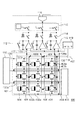
本実施形態における放射線検出装置100は、ガラス基板等の絶縁基板101上に、行方向及び列方向に配列された複数の画素102を含む画素領域103が設けられている。各画素102は、放射線又は光を電荷に変換する変換素子104と、変換素子104の電荷に応じた電気信号を出力するスイッチ素子105と、を含む。本実施形態では、変換素子としてMIS型光電変換素子を用いており、スイッチ素子として薄膜トランジスタ(TFT)を用いている。変換素子が放射線を電荷に変換することが求められる場合には、光電変換素子の放射線入射側に、放射線を光電変換素子が感知可能な可視光に波長変換する蛍光体が配置され得る。変換素子104の第1電極Lには、スイッチ素子105の第1主電極が電気的に接続され、変換素子104の第2電極Uには、バイアス線106が電気的に接続される。バイアス線106は、列方向に配列された複数の変換素子104の第2電極Uに共通に接続される。スイッチ素子105の制御電極には、駆動線107が電気的に接続され、スイッチ素子105の第2主電極には、信号線108が電気的に接続される。駆動線107は、行方向に配列された複数のスイッチ素子105の制御電極に共通に接続され、また、第1接続配線109を介して駆動回路110に電気的に接続される。駆動回路110が列方向に複数配列された駆動線107に駆動パルスを順次に又は同時に供給することにより、行単位で画素からの電気信号が、行方向に配列された複数の信号線105に並列に出力される。信号線105は、列方向に配列された複数のスイッチ素子105の第2主電極に共通に接続され、また、第2接続配線111を介して読出回路112に電気的に接続される。読出回路112は、信号線105毎に、信号線105からの電気信号を積分して増幅する積分増幅器113と、積分増幅器113で増幅して出力された電気信号をサンプルホールドするサンプルホールド回路を備える。読出回路112は更に、複数のサンプルホールド回路から並列に出力される電気信号を直列の電気信号に変換するマルチプレクサ115と、出力された電気信号をデジタルデータに変換するA/D変換器116を含む。読出回路112の非反転入力端子には電源回路119から基準電位Vrefが供給される。電源回路109は更に、共通バイアス線117及び第3接続配線118を介して、行方向に配列された複数のバイアス線106に電気的に接続されており、変換素子104の第2電極Uにバイアス電位Vs又は初期化電位Vrを供給する。
In the
次に、図1を用いて本実施形態の検出装置の動作について説明する。変換素子104の第1電極Lにはスイッチ素子を介して基準電位Vrefを与え、第2電極Uにはバイアス電位Vsを与えることにより、MIS型光電変換素子の光電変換層が空乏化するようなバイアスを変換素子104に与える。この状態で、被検体に向けて曝射された放射線は、被検体により減衰を受けて透過し、ここでは図示しない蛍光体で可視光に変換され、この可視光が光電変換素子に入射し、電荷に変換される。この電荷に応じた電気信号は、駆動回路110から駆動線107に印加される駆動パルスによりスイッチ素子105が導通状態となることで、信号線108に出力され、読出回路112によりデジタルデータとして外部に読み出される。その後、バイアス線106の電位をバイアス電位Vsから初期化電位Vrに変化させてスイッチ素子105を導通状態とすることにより、光電変換素子で発生し残留した正又は負のキャリアが除去される。その後、バイアス線106の電位を初期化電位Vrからバイアス電位Vsに変化させることにより、変換素子104の初期化がなされる。
Next, the operation of the detection apparatus of this embodiment will be described with reference to FIG. The reference potential Vref is applied to the first electrode L of the
以下に、図2を用いて画素の層構成を説明する。ここで、図2(b)〜(d)はそれぞれ、図2(a)中のA−A’、B−B’、C−C’の断面図である。図2(a)に示すように、本実施形態の放射線検出装置の1画素内には、変換素子104である光電変換素子と、スイッチ素子105であるTFTと、信号線108の一部と、駆動線107の一部と、バイアス線106の一部が配置されている。また、図2(b)〜(d)に示すように、スイッチ素子105であるTFTは、絶縁基板101上に形成された第1導電層201、第1絶縁層202、第1半導体層203、第1不純物半導体層204、第2導電層205から構成されている。第1導電層201はTFTの制御電極(ゲート電極)として、第1絶縁層202はゲート絶縁膜として用いられている。また、第1半導体層203はTFTのチャネルとして、第1不純物半導体層204はオーミックコンタクト層として、第2導電層205は第1又は第2主電極(ソース又はドレイン電極)として用いられている。
Hereinafter, the layer structure of the pixel will be described with reference to FIG. Here, FIGS. 2B to 2D are cross-sectional views taken along lines A-A ′, B-B ′, and C-C ′ in FIG. As shown in FIG. 2A, within one pixel of the radiation detection apparatus of the present embodiment, a photoelectric conversion element that is the
それらの上層には、第2絶縁層206と第3絶縁層207が配置されており、信号線108として用いられる第3導電層208が、第2絶縁層206及び第3絶縁層207の中に形成されている。つまり、第3導電層208は、第2絶縁層206及び第3絶縁層207に埋め込まれており、第3導電層208の最上位表面は第3絶縁層207の最上位表面と概略同一表面を構成している。そして、第2導電層205上における第2絶縁層206の膜厚と第3絶縁層207の膜厚の和は、第3導電層208の膜厚と概略等しくされている。また、スイッチ素子105の第2主電極となる第2導電層205は、信号線108となる第3導電層208と接続される。ここで、最上位表面とは、各配線となる導電層又は各絶縁層において変換素子から最も近い表面である。
A second insulating
第3絶縁層207及び第3導電層208の上層には、第4絶縁層209が配置されており、第4絶縁層209には第4導電層210が埋め込まれており、第4導電層210の最上位表面は第4絶縁層209の最上位表面と概略同一表面を構成している。そのため、第4絶縁層209と第4導電層210の膜厚は概略等しくされている。第4絶縁層209及び第4導電層210の上層には第5絶縁層211が配置されており、駆動線107として用いられる第5導電層212が、概略等しい膜厚の第2絶縁層211に埋め込まれている。それにより、第5導電層212の最上位表面は第5絶縁層211の最上位表面と概略同一表面を構成している。ここで、第4導電層210は、スイッチ素子105の第1主電極となる第2導電層205と変換素子104の第2電極Lとなる第6導電層214を接続するための接続電極である。また第4導電層210は、スイッチ素子105の制御電極となる第1導電層201と駆動線107となる第5導電層212を接続するための接続電極である。
A fourth insulating
その上層には、第6絶縁層213を介して、変換素子104としてMIS型光電変換素子が形成されている。MIS型光電変換素子は、第6導電層214、第7絶縁層215、第2半導体層216、第2不純物半導体層217、第8導電層219から構成されている。第6導電層214は光電変換素子の下電極(第1電極L)として、第7絶縁層215は発生した正及び負のキャリアの移動をブロックする完全絶縁層として、第2半導体層216は放射線又は光を電荷に変換する光電変換層として用いられる。また、第2不純物半導体層217は正又は負のキャリアの移動をブロックするブロッキング層として、第8導電層219は上電極(第2電極U)として用いられている。また、第7導電層218はバイアス線106として用いられる。そして、第8導電層219からなる上電極(第2電極U)は、バイアス線106から供給されるバイアス電位Vs又は初期化電位Vrと、第1電極Lに供給される基準電位Vrefとの電位差であるバイアスを、変換素子104全体に印加する電極として用いられる。
In the upper layer, a MIS photoelectric conversion element is formed as the
以上のように、本実施形態の放射線検出装置は、絶縁基板101上にスイッチ素子105、信号線108、ゲート線107、変換素子104、バイアス線106が順次配置される。また、更にその上層には、第8絶縁層220、保護層(不図示)、蛍光体(不図示)が配置される。これらにより1つの画素が構成される。つまり、本実施形態の検出装置は、スイッチ素子の上方に変換素子が配置された積層型の放射線検出装置である。
As described above, in the radiation detection apparatus of this embodiment, the
上述のように、本実施形態では、スイッチ素子105であるTFTの第1主電極及び第2主電極と、信号線108を別々の層で形成している。そして、信号線108となる第3導電層208を第2絶縁層206及び第3絶縁層207に埋め込んで配置してある。それにより、信号線となる第3導電層208を厚く形成することが可能である。そのため、小画素ピッチ化及び多画素化が要求される放射線検出装置において、それに応じて線幅を細くした場合でも、信号線108の抵抗増加を防止することが可能となる。また、信号線108は、駆動線107との交差部で容量を形成し、また変換素子104の第1電極Lとの交差部で容量を形成する。しかしながら、本実施形態のように信号線108が細い場合には、交差部での重なり面積が小さくなり、これら交差部での容量が小さくなる。また、信号線108と駆動線107の重なり面積に比べ、信号線108と変換素子104の第1電極Lとの重なり面積の方が大きい。そこで、信号線108の更なる容量低減のため、信号線108は、変換素子104の下方に配置された駆動線107となる導電層の最上位表面よりも下層の絶縁部材である第2絶縁層206及び第3絶縁層207に埋め込んで配置された第3導電層208からなる。それにより、信号線108の最上位表面を駆動線107の最上位表面よりも変換素子から離間して配置している。そのため、信号線108と変換素子との交差部による容量が低減される。更に、本実施形態では、第4導電層210を第4絶縁層209に埋め込んで配置しており、第5導電層212を第5絶縁層211に埋め込んで配置している。そのため、信号線108と駆動線107の間に配置された第4絶縁層209を、また、信号線108と変換素子104の第1電極Lとの間に配置された第4絶縁層209及び第5絶縁層212を厚く形成できる。そのため、信号線108と駆動線107との交差部の容量及び信号線108と変換素子104の第1電極Lとの交差部の容量を小さくすることが可能である。その結果、小画素ピッチ化及び多画素化が要求され、信号線108と重なる駆動線107及び変換素子104の数が増えた場合でも、信号線108は低抵抗で且つ低容量となり、信号線容量に起因するノイズの増加を防止することが可能となる。また、信号線108の線幅を細くすることが可能となるため、信号線108と駆動線107の交差部における駆動線107の容量も小さくすることができる。
As described above, in the present embodiment, the first main electrode and the second main electrode of the TFT that is the
一方、スイッチ素子105であるTFTの制御電極と駆動線107を別々の導電層で形成している。そして、駆動線107となる第5導電層212を、第5絶縁層211に埋め込んで配置している。このため、駆動線107となる第5導電層212を厚く形成することが可能であり、レイアウトの関係上、線幅を太くすることが困難な場合でも駆動線107の低抵抗化を実現できる。また、駆動線107を厚く形成することが可能となるため、抵抗を増加することなく駆動線107を細くできる。そのため、駆動線107を細くすることで、信号線106との重なり面積が減り、駆動線107の容量のうち、信号線との重なりに起因する容量の低減が可能である。更に、駆動線107と変換素子の第1電極Lとの距離は短くなってしまうが、駆動線107の線幅を細くすることが可能となるため、駆動線107と第1電極Lの交差部の面積が小さくできる。そのため、駆動線107と第1電極Lの交差部の容量が著しく増加することを防止できる。その結果、小画素ピッチ化及び多画素化が要求され、駆動線107と重なる信号線108及び変換素子104の数が増えた場合でも、駆動線107は低抵抗で且つ低容量となり、駆動線の時定数の増加を防止することが可能となる。
On the other hand, the control electrode of TFT which is the
以上のことから、本実施形態により、低ノイズであり、かつ高速駆動が可能な積層型の検出装置を実現できる。 From the above, according to the present embodiment, it is possible to realize a stacked type detection apparatus that is low noise and capable of high-speed driving.
なお、図1には3×3画素を示しているが、実際には例えば2000×2000画素が配置されて放射線検出装置を構成している。また本実施形態において、光電変換素子と蛍光体と組み合わせた間接型の放射線検出装置を示したが、本発明はこれに限定されるものではない。光電変換素子に代えて、X線,γ線、あるいはα線,β線などの粒子線を直接電荷に変換するアモルファスセレン等の半導体層を電極間に挟んだ変換素子を用いた直接型の放射線検出装置においても同様の効果が得られる。また、間接型の放射線検出装置の変換素子は、MIS型光電変換素子とは別の光電変換素子、例えばPIN型のフォトダイオードを用いてもかまわない。 Although FIG. 1 shows 3 × 3 pixels, actually, for example, 2000 × 2000 pixels are arranged to constitute a radiation detection apparatus. Moreover, in this embodiment, although the indirect type | mold radiation detection apparatus combined with the photoelectric conversion element and fluorescent substance was shown, this invention is not limited to this. Direct radiation using a conversion element in which a semiconductor layer such as amorphous selenium that directly converts particle beams such as X-rays, γ-rays, α-rays, and β-rays into electric charges is sandwiched between electrodes instead of photoelectric conversion elements. Similar effects can be obtained in the detection apparatus. Further, a photoelectric conversion element different from the MIS type photoelectric conversion element, for example, a PIN type photodiode may be used as the conversion element of the indirect radiation detection apparatus.
(第2の実施形態)
以下に、本発明の第2の実施形態について、図3を用いて説明する。図3は、図2(a)中の、A−A’、B−B’、C−C’の断面図である。その他第1の実施形態と同じものには同じ番号を付与し、ここでは説明を省略する。なお、本実施形態においては、画素の層構成についても、第1実施形態と同様であるが、絶縁層の特性を利用し、信号線108となる第3導電層208と駆動線107となる第5導電層212の形状を制御している点が第1の実施形態と異なる。
(Second Embodiment)
Below, the 2nd Embodiment of this invention is described using FIG. FIG. 3 is a cross-sectional view taken along the lines AA ′, BB ′, and CC ′ in FIG. The same components as those in the first embodiment are denoted by the same reference numerals, and the description thereof is omitted here. In this embodiment, the layer structure of the pixel is the same as that of the first embodiment. However, the third
まず、図3(a)〜(c)を用いて信号線108となる第3導電層208の形状について説明する。第2絶縁層206には無機膜を、第3絶縁層207にはネガ型の感光性を有する有機絶縁膜を用いている。ここで、第2絶縁層206となる無機膜、第3絶縁層207となる有機絶縁膜を順に成膜し、有機絶縁膜を光照射によりパターニングして第3絶縁層207を形成する。続いて、第3絶縁層207をマスクとして無機膜にエッチングを実施し第2絶縁層206を形成する。その後、第3導電層208となる導電膜を成膜し、表面研磨により不要な部分の導電膜を削り取ることで、信号線108となる第3導電層208は第2絶縁層206及び第3絶縁層208の中に形成される。このように形成されることにより、信号線108の上部幅をST、最大幅をSMとした場合、ST<SMとなる。
First, the shape of the third
次に、駆動線107となる第5導電層212の形状について説明する。第4絶縁層209及び第4導電層210を形成した後、第5絶縁層211を形成する。第5絶縁層211には、ポジ型の感光性を有する有機絶縁膜を用いており、有機絶縁膜を成膜した後、光照射によりパターニングして第5絶縁層211を形成する。続いて、第5導電層212となる導電膜を成膜し、表面研磨により不要な部分の導電膜を削り取ることで、駆動線107となる第5導電層212は図3のように、第5絶縁層211内に形成される。このように形成されることにより、駆動線107の下部幅をGB、最大幅をGMとした場合、GB<GMとなる。
Next, the shape of the fifth
以上のように、信号線108の形状をその線幅の関係がST<SMとなるように制御することにより、信号線108と駆動線107の重なり面積、または信号線108と変換素子104の重なり面積が低減する。そのため、第1の実施形態に対して、本実施形態は更なる信号線容量の低減が可能となる。また、駆動線107の形状をその線幅がGB<GMとなるように制御することにより、信号線108と駆動線107の重なり面積が低減する。そのため、第1の実施形態に対して、本実施形態は更なる信号線容量と駆動線容量の低減が可能となる。結果、より低ノイズであり、かつ高速駆動が可能な積層型の放射線検出装置を実現できる。
As described above, by controlling the shape of the
なお、本実施形態では、信号線108及び駆動線をそれぞれ有機絶縁膜の中に形成したが、有機絶縁膜の上層に例えば無機絶縁膜を形成することで、表面研磨時に有機絶縁膜の削れを防止できる。即ち、研磨のストッパー層として有機絶縁膜上に無機絶縁膜を配置することで、更なる加工精度の向上が可能である。
In the present embodiment, the
(第3の実施形態)
以下に、本発明の第3の実施形態について、図面を用いて説明する。図4は本実施形態の等価回路図、図5(a)は本実施形態の1画素の平面図、図5(b)〜(d)はそれぞれ図5(a)中のD−D’、E−E’、F−F’の断面図である。なお、第1の実施形態と同じものには同じ番号を付与し、ここでは説明を省略する。
(Third embodiment)
Below, the 3rd Embodiment of this invention is described using drawing. 4 is an equivalent circuit diagram of the present embodiment, FIG. 5A is a plan view of one pixel of the present embodiment, and FIGS. 5B to 5D are DD ′ in FIG. It is sectional drawing of EE 'and FF'. In addition, the same number is given to the same thing as 1st Embodiment, and description is abbreviate | omitted here.
本実施形態の画素102は、変換素子104を初期化するための初期化用スイッチ素子401を更に含んでいる。初期化用スイッチ素子401の制御端子は初期化用駆動線402に、初期化用スイッチ素子401の第1主電極は変換素子104の第1電極Lに、初期化用スイッチ素子401の第2主電極は初期化用バイアス線403に、それぞれ電気的に接続される。初期化用駆動線402は行方向に配列された複数の初期化用スイッチ素子401の制御電極に共通に接続され、第4接続配線404を介して初期化用駆動回路405に電気的に接続される。初期化用駆動回路405が列方向に複数配列された初期化用駆動線402に駆動パルスを順次に又は同時に供給することにより、行単位で変換素子401の初期化を行う。初期化用バイアス線403は列方向に配列された複数の初期化用スイッチ素子401の第2主電極に共通に接続される。また、電源回路119は、共通初期化バイアス線406及び第5接続配線407を介して、行方向に配列された複数の初期化バイアス線403に電気的に接続されており、変換素子104の第1電極Lに初期化用電位Vtを供給する。一方、本実施形態の電源回路119は、変換素子104の第2電極Uに対しては、共通バイアス線117及び第3接続配線118を介してバイアス電位Vsのみを供給する。
The
次に、図4を用いて本実施形態の検出装置の動作について説明する。まず、変換素子104の第1電極Lにはスイッチ素子を介して基準電位Vrefを与え、第2電極Uにはバイアス電位Vsを与えることにより、MIS型光電変換素子の光電変換層が空乏化するようなバイアスを変換素子に与える。この状態で、被検体に向けて曝射された放射線は、被検体により減衰を受けて透過し、ここでは図示しない蛍光体で可視光に変換され、この可視光が光電変換素子に入射し、電荷に変換される。この電荷に応じた電気信号は、駆動回路110から駆動線107に印加される駆動パルスにより信号出力用のスイッチ素子105が導通状態となることで、信号線108に出力され、読出回路112によりデジタルデータとして外部に読み出される。その後、初期化用駆動回路405から初期化用駆動線402に駆動パルスが印加され、初期化用スイッチ素子401を導通状態にする。これにより初期化バイアス線403を介して変換素子104の第1電極Lに初期化用電位Vtが供給される。変換素子104を初期化するためのバイアスVs−Vtが変換素子104に印加されることにより、変換素子104で発生し残留した正又は負のキャリアが除去される。その後、変換素子104の第1電極Lの電位を初期化電位Vtからバイアス電位Vrefに変化させることにより、変換素子104の初期化がなされる。以上の動作を行単位で繰り返すことにより、1画像の画像信号が得られ、更にこの一連の動作を繰り返すことで動画像が得られる。
Next, operation | movement of the detection apparatus of this embodiment is demonstrated using FIG. First, the reference potential Vref is applied to the first electrode L of the
以下に、図5を用いて画素の層構成を説明する。図5(a)に示すように、本実施形態の放射線検出装置の1画素内には、変換素子104と、信号出力用のスイッチ素子105と、初期化用スイッチ素子401と、が配置されている。1画素内には更に、信号線108の一部と、駆動線107の一部と、初期化用駆動線402の一部と、初期化用バイアス線403の一部と、バイアス線106の一部が配置されている。また、図5(b)〜(d)に示すように、スイッチ素子105と初期化用スイッチ素子401は、絶縁基板101上の第1絶縁層501、第1半導体層502、第2絶縁層503、第1導電層504、第3絶縁層505、第2導電層506から構成される。第1導電層504はTFTの制御電極(ゲート電極)として、第2絶縁層503はゲート絶縁膜として用いられている。また、第1半導体層502はTFTのチャネルとして用いられるポリシリコンであり、第2導電層506は第1又は第2主電極(ソース又はドレイン電極)として用いられている。
Hereinafter, the layer structure of the pixel will be described with reference to FIG. As shown in FIG. 5A, a
それらの上層には、第4絶縁層507と第5絶縁層508が配置されており、信号線108及び初期化用バイアス線403として用いられる第3導電層509が、第4絶縁層507及び第5絶縁層508の中に形成されている。また、第2導電層506で構成されるスイッチ素子105の第2主電極と初期化用スイッチ素子401の第2主電極は、信号線108及び初期化用バイアス線403として用いられる第3導電層509と接続される。ここで、第4絶縁層507にポジ型の感光性を有する有機絶縁膜を用い、第5絶縁層508にネガ型の感光性を有する有機絶縁膜を用いる。それにより、信号線108及び初期化用バイアス線403の上部幅をST、最大幅をSMとした場合、ST<SMとなる。
A fourth insulating
その上層には、ポジ型の感光性を有する有機絶縁膜である第6絶縁層510が配置されており、第4導電層511が第6絶縁層510に埋め込まれて配置されている。その上層には第7絶縁層512、第8絶縁層513が配置されており、駆動線107又は初期化用駆動線402として用いられる第5導電層514が、第7絶縁層512及び第8絶縁層513の中に形成されている。ここで、第7絶縁層512にポジ型の感光性を有する有機絶縁膜を用い、第8絶縁層513にネガ型の感光性を有する有機絶縁膜を用いる。それにより、駆動線107又は初期化用駆動線402の上部幅をGT、下部幅をGB、最大幅をGMとした場合、GB<GM、かつGT<GMとなる。第4導電層511は、スイッチ素子105又は初期化用スイッチ素子401の第1主電極となる第2導電層506と変換素子104の第2電極Lとなる第6導電層516とを接続するための接続電極である。また第4導電層511は、スイッチ素子105又は初期化用スイッチ素子401の制御電極となる第1導電層504と駆動線107又は初期化用駆動線402となる第5導電層514とを接続するための接続電極である。
A sixth insulating
その上層には、第9絶縁層515を介して、変換素子104としてMIS型光電変換素子が形成されている。MIS型光電変換素子は、第6導電層516、第10絶縁層517、第2半導体層518、不純物半導体層519、第8導電層521から構成されている。第6導電層516は光電変換素子の下電極(第1電極L)として、第10絶縁層517は発生した正及び負のキャリアの移動をブロックする完全絶縁層として、第2半導体層518は放射線又は光を電荷に変換する光電変換層として用いられる。また、不純物半導体層519は正又は負のキャリアの移動をブロックするブロッキング層として、第8導電層521は上電極(第2電極U)として用いられている。また、第7導電層520はバイアス線106として用いられる。そして、第8導電層521からなる上電極(第2電極U)は、バイアス線106から供給されるバイアス電位Vsと、第1電極Lに供給される基準電位Vref又は初期化電位Vtとの電位差であるバイアスを、変換素子104全体に印加する電極として用いられる。
In the upper layer, a MIS type photoelectric conversion element is formed as the
以上のように、ネガ型、またはポジ型の感光性を有する複数の絶縁層の中に各配線を形成することにより、各配線の形状を容易に制御することができる。これにより、信号線容量の低減が可能となる。また、本実施例では駆動線107の上部幅GTが最大幅GMより小さいため、実施形態1又は2に比べて、駆動線と変換素子の下電極(第1電極L)との重なり面積が減少する。そのため、駆動線と変換素子との交差部での容量が低減する。結果、抵抗と容量の積で決まる駆動線の時定数が小さくなり、更なる高速駆動が可能となる。
As described above, by forming each wiring in a plurality of insulating layers having negative or positive photosensitivity, the shape of each wiring can be easily controlled. As a result, the signal line capacitance can be reduced. In this example, since the upper width GT of the
(第4の実施形態)
以下に、本発明の第4の実施形態について、図面を用いて説明する。図6は等価回路図、図7(a)、(b)は1画素の平面図、図7(c)〜(f)は図7(a)、(b)中のG−G’、H−H’、I−I’、J−J’の断面図である。その他、第3の実施形態と同じものには同じ番号を付与し、ここでは説明を省略する。
(Fourth embodiment)
Below, the 4th Embodiment of this invention is described using drawing. 6 is an equivalent circuit diagram, FIGS. 7A and 7B are plan views of one pixel, and FIGS. 7C to 7F are GG ′ and H in FIGS. 7A and 7B. It is sectional drawing of -H ', II', and JJ '. In addition, the same number is given to the same thing as 3rd Embodiment, and description is abbreviate | omitted here.
本実施形態の放射線検出装置は、第3の実施形態に対して更に小画素ピッチ化に対応するものである。小画素ピッチ化のために各配線を細くした場合でも、1画素内における接続ホールの占める割合が大きくなり、信号出力用のスイッチ素子と初期化用スイッチ素子の接続ホールが重なるおそれがある。ここで、接続ホールとは、各スイッチ素子の電極と各配線とを接続するためのホールである。 The radiation detection apparatus according to the present embodiment further corresponds to a smaller pixel pitch than the third embodiment. Even when each wiring is thinned to reduce the pixel pitch, the proportion of connection holes in one pixel increases, and there is a possibility that the connection holes of the signal output switch element and the initialization switch element overlap. Here, the connection hole is a hole for connecting the electrode of each switch element and each wiring.
上記問題を解決するため、本実施形態では、図7(a)に示す第1画素Aと図7(b)に示す第2画素Bとを、交互に配置している。なお、第2画素Bは、画素Aを180度回転させた画素である。層構成は第3の実施形態と同様であるが、接続ホールの配置位置、及び各配線の構造がと異なる。 In order to solve the above problem, in the present embodiment, the first pixels A shown in FIG. 7A and the second pixels B shown in FIG. 7B are alternately arranged. The second pixel B is a pixel obtained by rotating the pixel A by 180 degrees. The layer configuration is the same as in the third embodiment, but the arrangement positions of the connection holes and the structures of the respective wirings are different.
以下に、第3の実施形態と異なる点を詳細に説明する。まず、本実施形態では、1列分の信号線108は、第2導電層506からなる第1信号線108aと、第5絶縁層508中の第3導電層509からなる第2信号線108bと、を含む。また1列分の初期化用バイアス線403は、第2導電層506からなる第1初期化用バイアス線403aと、第5絶縁層508中の第3導電層509からなる第2初期化用バイアス線403bと、を含む。これらに対して、第4絶縁層507中の第3導電層509が接続ホールを形成している。一方、1行分の駆動線107は、第1導電層504からなる第1駆動線107aと、第5導電層514からなる第2駆動線107bと、を含む。また、1行分の初期化用駆動線402は、第1導電層504からなる第1初期化用駆動線402aと、第5導電層514からなる第2初期化用駆動線402bと、を含む。これらに対して、第3導電層509と第4導電層511が接続ホールを形成している。
The differences from the third embodiment will be described in detail below. First, in the present embodiment, the
次に、第1画素Aでは、信号出力用のスイッチ素子105の制御電極と第2駆動線107bとを接続するための接続ホールと、第2主電極と第2信号線108bとを接続するための接続ホールと、が配置されている。そのため、スイッチ素子105の制御電極は第1駆動線107aと第2駆動線107bの両方に接続されており、第2主電極は第1信号線108aと第2信号線108bの両方に接続されている。一方、初期化用スイッチ素子401の制御電極と第2初期化用駆動線402bとを接続するための接続ホールと、第2主電極と第2初期化用バイアス線403bとを接続するための接続ホールと、は配置されていない。そのため、初期化用スイッチ素子401の制御電極は第1初期化用駆動線402aにのみ接続されており、第2主電極は第1初期化用バイアス線403aにのみ接続されている。これに対して第2画素Bでは、信号出力用のスイッチ素子105の制御電極と第2駆動線107bとを接続するための接続ホールと、第2主電極と第2信号線108bとを接続するための接続ホールと、は配置されていない。そのため、スイッチ素子105の制御電極は第1駆動線107aのみに接続されており、第2主電極は第1信号線108aのみに接続されている。一方、初期化用スイッチ素子401の制御電極と第2初期化用駆動線402bとを接続するための接続ホールと、第2主電極と初期化用バイアス線403bとを接続するための接続ホールと、が配置されている。そのため、初期化用スイッチ素子401の制御電極は第1初期化用駆動線402aと第2初期化用駆動線402bの両方に接続されており、第2主電極は第1初期化用バイアス線403aと第2初期化用バイアス線403bの両方に接続されている。この、接続ホールの配置位置の異なる2種類の画素を交互に配置している点が第3の実施形態と異なる。
Next, in the first pixel A, a connection hole for connecting the control electrode of the signal
以上のように、画素Aと画素Bを交互に配置することにより、1画素内の接続ホールの数を削減できるため、更なる小画素ピッチ化が要求される場合でも、1画素内に複数のスイッチ素子を配置することが可能となる。また、第3の実施形態と同様に、信号線容量及び抵抗の低減、及び駆動線の抵抗低減が更に可能となり、低ノイズで、かつ高速駆動が可能な積層型の放射線検出装置を実現できる。なお、本実施形態は2種類の画素を交互に配置しているが、本実施形態はこれに限定されるものではなく、接続ホールの配置位置が異なる画素を複数種設け、これを組み合わせることで、同様の効果が得られる。 As described above, by alternately arranging the pixel A and the pixel B, the number of connection holes in one pixel can be reduced. Therefore, even when a further smaller pixel pitch is required, a plurality of pixels are included in one pixel. A switch element can be arranged. Further, similarly to the third embodiment, the signal line capacitance and resistance can be further reduced, and the resistance of the drive line can be further reduced, so that a stacked radiation detection apparatus that can be driven at high speed with low noise can be realized. In this embodiment, two types of pixels are alternately arranged. However, this embodiment is not limited to this, and a plurality of types of pixels having different connection hole arrangement positions are provided and combined. A similar effect can be obtained.
(第5の実施形態)
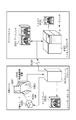
図8は本発明による放射線検出装置を用いた放射線検出システムへの応用例を示したものである。
(Fifth embodiment)
FIG. 8 shows an application example to a radiation detection system using the radiation detection apparatus according to the present invention.
図8に示すように、放射線源であるX線チューブ6050で発生したX線6060は患者あるいは被験者6061の胸部6062を透過し、蛍光体を上部に実装した放射線検出装置6040に入射する。この入射したX線には患者6061の体内部の情報が含まれている。X線の入射に対応して蛍光体は発光し、これを光電変換して、電気的情報を得る。この情報はディジタルに変換され信号処理手段となるイメージプロセッサ6070により画像処理され、制御室の表示手段となるディスプレイ6080で観察できる。
As shown in FIG. 8,
また、この情報は電話回線6090等の伝送処理手段により遠隔地へ転送でき、別の場所のドクタールームなどに設置された表示手段となるディスプレイ6081に表示もしくは光ディスク等の記録手段に保存でき、遠隔地の医師が診断することも可能である。また記録手段となるフィルムプロセッサ6100により記録媒体となるフィルム6110に記録することもできる。
This information can be transferred to a remote location by transmission processing means such as a
100 検出装置
101 絶縁基板
102 画素
103 画素領域
104 変換素子
105 スイッチ素子
106 バイアス線
107 駆動線
108 信号線
201 第1導電層
202 第1絶縁層
203 第1半導体層
204 第1不純物半導体層
205 第2導電層
206 第2絶縁層
207 第3絶縁層
208 第3導電層
209 第4絶縁層
210 第4導電層
211 第5絶縁層
212 第5導電層
213 第6絶縁層
214 第6導電層
215 第7絶縁層
216 第2半導体層
217 第2不純物半導体層
218 第7導電層
219 第8導電層
220 第8絶縁層
DESCRIPTION OF
Claims (9)
前記行方向の複数の前記スイッチ素子に接続された駆動線と、
前記列方向の複数の前記スイッチ素子に接続された信号線と、を有し、
前記変換素子が前記スイッチ素子の上方に配置された検出装置であって、
前記駆動線は、前記変換素子と前記スイッチ素子の間の絶縁部材に埋め込んで配置された導電層からなり、
前記信号線は、前記駆動線の最上位表面よりも下層で前記スイッチ素子と前記駆動線との間に配置された絶縁部材に埋め込んで配置された導電層からなることを特徴とする検出装置。 A plurality of pixels arranged in a row direction and a column direction, each including a conversion element that converts radiation or light into an electric charge, and a switch element that outputs an electric signal corresponding to the electric charge;
Drive lines connected to the plurality of switch elements in the row direction;
A signal line connected to the plurality of switch elements in the column direction,
The conversion device is a detection device disposed above the switch element,
The drive line is composed of a conductive layer disposed in an insulating member between the conversion element and the switch element,
The detection apparatus according to claim 1, wherein the signal line includes a conductive layer embedded in an insulating member disposed below the uppermost surface of the drive line and between the switch element and the drive line .
前記絶縁部材は、前記複数の絶縁層のうち、前記変換素子の下方に配置された前記駆動線となる導電層の最上位表面よりも下層の絶縁層であることを特徴とする請求項1に記載の検出装置。 A plurality of insulating layers between the conversion element and the switch element disposed on an insulating substrate;
2. The insulating member according to claim 1, wherein the insulating member is an insulating layer lower than an uppermost surface of a conductive layer serving as the drive line arranged below the conversion element among the plurality of insulating layers. The detection device described.
前記信号線は、前記スイッチ素子の上の第2絶縁層と、前記第2絶縁層の上の第3絶縁層と、に埋め込んで配置された第3導電層からなり、
前記駆動線は、前記第3導電層と、前記第3絶縁層の上の第4絶縁層に埋め込んで配置された第4導電層と、によって前記スイッチ素子に接続され、前記第4絶縁層の上の第5絶縁層に埋め込んで配置された第5導電層からなり、
前記信号線と前記駆動線とが交差する領域では、前記信号線は前記第3導電層からなり、前記駆動線は前記第5導電層からなり、前記第4絶縁層を挟んで前記信号線と前記駆動線が交差しており、
前記変換素子は、前記第3導電層と前記第4導電層と前記第5導電層とによって前記スイッチ素子に接続され、前記第5絶縁層の上の第6絶縁層を介して配置された第7導電層を下電極として有する請求項2に記載の検出装置。 The switch element includes a first conductive layer on the insulating substrate, a first insulating layer on the first conductive layer, a first semiconductor layer on the first insulating layer, and the first semiconductor layer. A first impurity semiconductor layer above the first impurity semiconductor layer, and a second conductive layer above the first impurity semiconductor layer,
The signal line includes a third conductive layer disposed so as to be embedded in a second insulating layer on the switch element and a third insulating layer on the second insulating layer,
The drive line is connected to the switch element by the third conductive layer and a fourth conductive layer disposed in the fourth insulating layer on the third insulating layer, and the drive line is connected to the switch element. Comprising a fifth conductive layer disposed embedded in an upper fifth insulating layer;
In the region where the signal line and the drive line intersect, the signal line is made of the third conductive layer, the drive line is made of the fifth conductive layer, and the signal line is sandwiched by the fourth insulating layer. The drive lines intersect,
The conversion element is connected to the switch element by the third conductive layer, the fourth conductive layer, and the fifth conductive layer, and is disposed via a sixth insulating layer on the fifth insulating layer. The detection device according to claim 2, comprising 7 conductive layers as lower electrodes.
前記行方向の複数の前記初期化用スイッチ素子に接続された初期化用駆動線と、
前記列方向の複数の前記初期化用スイッチ素子に接続された初期化用バイアス線と、
を更に含む請求項2に記載の検出装置。 The pixel further includes an initialization switch element that initializes the conversion element,
An initialization drive line connected to the plurality of initialization switch elements in the row direction;
An initialization bias line connected to the plurality of initialization switch elements in the column direction;
The detection device according to claim 2, further comprising:
前記信号線は、前記スイッチ素子の上の第4絶縁層の上の第5絶縁層に埋め込んで配置された第3導電層を含み、
前記駆動線は、前記第3導電層と、前記第5絶縁層の上の第6絶縁層に埋め込んで配置された第4導電層と、によって前記スイッチ素子に接続され、前記第6絶縁層の上の第7絶縁層に埋め込んで配置された第5導電層を含み、
前記信号線と前記駆動線とが交差する領域では、前記信号線は前記第3導電層からなり、前記駆動線は前記第5導電層からなり、前記第4絶縁層を挟んで前記信号線と前記駆動線が交差していることを特徴とする請求項4に記載の検出装置。 The switch element includes a first insulating layer on the insulating substrate, a first semiconductor layer on the first insulating layer, a second insulating layer on the first insulating layer, and the second insulating layer. A first conductive layer above the first conductive layer; a third insulating layer above the first conductive layer; and a second conductive layer above the third insulating layer;
The signal line includes a third conductive layer disposed in a fifth insulating layer on the fourth insulating layer on the switch element;
The drive line is connected to the switch element by the third conductive layer and a fourth conductive layer disposed in a sixth insulating layer on the fifth insulating layer, and the drive line is connected to the switch element. A fifth conductive layer disposed embedded in the seventh insulating layer;
In the region where the signal line and the drive line intersect, the signal line is made of the third conductive layer, the drive line is made of the fifth conductive layer, and the signal line is sandwiched by the fourth insulating layer. The detection device according to claim 4, wherein the drive lines intersect each other.
前記変換素子は、前記第3導電層と前記第4導電層と前記第5導電層とによって前記スイッチ素子に接続され、前記第8絶縁層の上の第9絶縁層を介して配置された第6導電層を下電極として有する請求項5に記載の検出装置。 The fifth conductive layer is further embedded in an eighth insulating layer above the seventh insulating layer,
The conversion element is connected to the switch element by the third conductive layer, the fourth conductive layer, and the fifth conductive layer, and is disposed via a ninth insulating layer on the eighth insulating layer. The detection device according to claim 5, comprising six conductive layers as lower electrodes.
ST<SM
を満たすことを特徴とする請求項1から6のいずれか1項に記載の検出装置。 When the upper width of the signal line is ST and the maximum width is SM,
ST <SM
Detection device according to any one of claims 1 to 6, characterized in that meet.
GB<GM
を満たすことを特徴とする請求項1から6のいずれか1項に記載の検出装置。 When the lower width of the drive line is GB and the maximum width is GM,
GB <GM
Detection device according to any one of claims 1 to 6, characterized in that meet.
前記検出装置からの信号を処理する信号処理手段と、
前記信号処理手段からの信号を記録するための記録手段と、
前記信号処理手段からの信号を表示するための表示手段と、
前記信号処理手段からの信号を伝送するための伝送処理手段と、
を具備することを特徴とする放射線検出システム。 The detection device according to any one of claims 1 to 8 ,
Signal processing means for processing a signal from the detection device;
Recording means for recording a signal from the signal processing means;
Display means for displaying a signal from the signal processing means;
Transmission processing means for transmitting a signal from the signal processing means;
A radiation detection system comprising:
Priority Applications (3)
| Application Number | Priority Date | Filing Date | Title |
|---|---|---|---|
| JP2010176365A JP5700973B2 (en) | 2010-08-05 | 2010-08-05 | Detection apparatus and radiation detection system |
| US13/195,535 US8759785B2 (en) | 2010-08-05 | 2011-08-01 | Detection apparatus and radiation detection system |
| CN201110218964XA CN102376725A (en) | 2010-08-05 | 2011-08-02 | Detection apparatus and radiation detection system |
Applications Claiming Priority (1)
| Application Number | Priority Date | Filing Date | Title |
|---|---|---|---|
| JP2010176365A JP5700973B2 (en) | 2010-08-05 | 2010-08-05 | Detection apparatus and radiation detection system |
Publications (3)
| Publication Number | Publication Date |
|---|---|
| JP2012038857A JP2012038857A (en) | 2012-02-23 |
| JP2012038857A5 JP2012038857A5 (en) | 2013-09-12 |
| JP5700973B2 true JP5700973B2 (en) | 2015-04-15 |
Family
ID=45555436
Family Applications (1)
| Application Number | Title | Priority Date | Filing Date |
|---|---|---|---|
| JP2010176365A Expired - Fee Related JP5700973B2 (en) | 2010-08-05 | 2010-08-05 | Detection apparatus and radiation detection system |
Country Status (3)
| Country | Link |
|---|---|
| US (1) | US8759785B2 (en) |
| JP (1) | JP5700973B2 (en) |
| CN (1) | CN102376725A (en) |
Families Citing this family (9)
| Publication number | Priority date | Publication date | Assignee | Title |
|---|---|---|---|---|
| KR102009801B1 (en) * | 2012-11-27 | 2019-08-12 | 엘지디스플레이 주식회사 | Thin Film Transistor array substrate for digital X-ray detector |
| CN103855172B (en) * | 2012-12-03 | 2016-11-23 | 群康科技(深圳)有限公司 | X-ray detector |
| JP6242211B2 (en) * | 2013-12-26 | 2017-12-06 | キヤノン株式会社 | Imaging apparatus and imaging system |
| US10276611B2 (en) | 2015-06-04 | 2019-04-30 | Sharp Kabushiki Kaisha | Photosensor substrate |
| CN105182396B (en) | 2015-06-29 | 2018-04-24 | 苏州瑞派宁科技有限公司 | A kind of channel multiplexing method that detector signal is read |
| JP6775408B2 (en) * | 2016-12-20 | 2020-10-28 | キヤノン株式会社 | Radiation imaging device and radiation imaging system |
| CN108318907B (en) * | 2018-02-01 | 2019-10-01 | 北京京东方光电科技有限公司 | X-ray detection panel and its manufacturing method and X-ray detection device |
| US11843022B2 (en) * | 2020-12-03 | 2023-12-12 | Sharp Kabushiki Kaisha | X-ray imaging panel and method of manufacturing X-ray imaging panel |
| US11916094B2 (en) * | 2021-08-02 | 2024-02-27 | Sharp Display Technology Corporation | Photoelectric conversion panel and method for manufacturing photoelectric conversion panel |
Family Cites Families (14)
| Publication number | Priority date | Publication date | Assignee | Title |
|---|---|---|---|---|
| JPH06318589A (en) * | 1993-05-10 | 1994-11-15 | Mitsubishi Electric Corp | Semiconductor integrated circuit device |
| JPH0964182A (en) * | 1995-08-25 | 1997-03-07 | Hitachi Ltd | Semiconductor integrated circuit device and manufacture thereof |
| JP3631380B2 (en) * | 1998-08-28 | 2005-03-23 | 株式会社東芝 | Semiconductor device and manufacturing method thereof |
| JP2002076360A (en) * | 2000-09-04 | 2002-03-15 | Canon Inc | Semiconductor device, its manufacturing method and radiation imaging system |
| JP4908947B2 (en) | 2005-07-11 | 2012-04-04 | キヤノン株式会社 | Conversion device, radiation detection device, and radiation detection system |
| JP5043373B2 (en) * | 2005-07-11 | 2012-10-10 | キヤノン株式会社 | Conversion device, radiation detection device, and radiation detection system |
| JP5043374B2 (en) * | 2005-07-11 | 2012-10-10 | キヤノン株式会社 | Conversion device, radiation detection device, and radiation detection system |
| CN100565894C (en) | 2005-07-11 | 2009-12-02 | 佳能株式会社 | Conversion equipment, radiation detecting apparatus and radiation detecting system |
| CN100511693C (en) | 2005-08-31 | 2009-07-08 | 佳能株式会社 | Radiation detecting apparatus, radiation imaging apparatus and radiation imaging system |
| JP5159065B2 (en) * | 2005-08-31 | 2013-03-06 | キヤノン株式会社 | Radiation detection apparatus, radiation imaging apparatus, and radiation imaging system |
| JP5328169B2 (en) * | 2007-02-28 | 2013-10-30 | キヤノン株式会社 | Imaging apparatus and radiation imaging system |
| JP2010003820A (en) * | 2008-06-19 | 2010-01-07 | Fujifilm Corp | Electromagnetic wave detection element |
| JP2012079820A (en) * | 2010-09-30 | 2012-04-19 | Canon Inc | Detector and radiation detection system |
| JP2012079860A (en) * | 2010-09-30 | 2012-04-19 | Canon Inc | Detector and radiation detection system |
-
2010
- 2010-08-05 JP JP2010176365A patent/JP5700973B2/en not_active Expired - Fee Related
-
2011
- 2011-08-01 US US13/195,535 patent/US8759785B2/en not_active Expired - Fee Related
- 2011-08-02 CN CN201110218964XA patent/CN102376725A/en active Pending
Also Published As
| Publication number | Publication date |
|---|---|
| JP2012038857A (en) | 2012-02-23 |
| US8759785B2 (en) | 2014-06-24 |
| CN102376725A (en) | 2012-03-14 |
| US20120032088A1 (en) | 2012-02-09 |
Similar Documents
| Publication | Publication Date | Title |
|---|---|---|
| JP5700973B2 (en) | Detection apparatus and radiation detection system | |
| JP5489542B2 (en) | Radiation detection apparatus and radiation imaging system | |
| JP5043380B2 (en) | Radiation detection apparatus and radiation detection system | |
| JP5159065B2 (en) | Radiation detection apparatus, radiation imaging apparatus, and radiation imaging system | |
| US8067743B2 (en) | Imaging apparatus and radiation imaging apparatus | |
| JP6570315B2 (en) | Radiation imaging apparatus and radiation imaging system | |
| US8680472B2 (en) | Radiation detecting apparatus and radiation imaging system | |
| JP4845352B2 (en) | Radiation imaging apparatus, manufacturing method thereof, and radiation imaging system | |
| JP5709810B2 (en) | Detection device manufacturing method, detection device and detection system | |
| JP2009043826A (en) | Imaging device and radiation imaging system | |
| JP2012079860A (en) | Detector and radiation detection system | |
| TW200814309A (en) | Radiation imaging apparatus and radiation imaging system | |
| JP2010056570A (en) | Radiation ray detection apparatus and driving method of the same, and photoelectric conversion device | |
| JP2013235934A (en) | Detection device, detection system and method for manufacturing detection device | |
| JP2007103578A (en) | Photoelectric converter and radiation detector | |
| JP4067055B2 (en) | Imaging apparatus and manufacturing method thereof, radiation imaging apparatus, and radiation imaging system | |
| US8405039B2 (en) | Detection apparatus and radiation detection system | |
| JP6530600B2 (en) | Radiation detection apparatus and radiation detection system | |
| JP2017098830A (en) | Radiation imaging device, radiation imaging system, and manufacturing method of radiation imaging device | |
| JP5677353B2 (en) | Radiation detection apparatus and radiation imaging system | |
| JP6719324B2 (en) | Radiation imaging apparatus and radiation imaging system | |
| JP5789223B2 (en) | Radiation imaging apparatus and radiation imaging system | |
| JP2006186031A (en) | Photoelectric conversion device and radiation imager | |
| JP2006005150A (en) | Imaging device and radiographic imaging device and radiographic imaging system | |
| JP2018195949A (en) | Radiation imaging device and radiation imaging system |
Legal Events
| Date | Code | Title | Description |
|---|---|---|---|
| A521 | Request for written amendment filed |
Free format text: JAPANESE INTERMEDIATE CODE: A523 Effective date: 20130729 |
|
| A621 | Written request for application examination |
Free format text: JAPANESE INTERMEDIATE CODE: A621 Effective date: 20130729 |
|
| A977 | Report on retrieval |
Free format text: JAPANESE INTERMEDIATE CODE: A971007 Effective date: 20140414 |
|
| A131 | Notification of reasons for refusal |
Free format text: JAPANESE INTERMEDIATE CODE: A131 Effective date: 20140422 |
|
| A521 | Request for written amendment filed |
Free format text: JAPANESE INTERMEDIATE CODE: A523 Effective date: 20140623 |
|
| TRDD | Decision of grant or rejection written | ||
| A01 | Written decision to grant a patent or to grant a registration (utility model) |
Free format text: JAPANESE INTERMEDIATE CODE: A01 Effective date: 20150120 |
|
| A61 | First payment of annual fees (during grant procedure) |
Free format text: JAPANESE INTERMEDIATE CODE: A61 Effective date: 20150217 |
|
| LAPS | Cancellation because of no payment of annual fees |