JP2009043826A - Imaging device and radiation imaging system - Google Patents
Imaging device and radiation imaging system Download PDFInfo
- Publication number
- JP2009043826A JP2009043826A JP2007205472A JP2007205472A JP2009043826A JP 2009043826 A JP2009043826 A JP 2009043826A JP 2007205472 A JP2007205472 A JP 2007205472A JP 2007205472 A JP2007205472 A JP 2007205472A JP 2009043826 A JP2009043826 A JP 2009043826A
- Authority
- JP
- Japan
- Prior art keywords
- conversion element
- signal
- line
- lines
- protective layer
- Prior art date
- Legal status (The legal status is an assumption and is not a legal conclusion. Google has not performed a legal analysis and makes no representation as to the accuracy of the status listed.)
- Granted
Links
- 238000003384 imaging method Methods 0.000 title claims abstract description 37
- 230000005855 radiation Effects 0.000 title claims description 41
- 238000006243 chemical reaction Methods 0.000 claims abstract description 45
- 239000011241 protective layer Substances 0.000 claims abstract description 30
- 239000010410 layer Substances 0.000 claims description 62
- 239000000758 substrate Substances 0.000 claims description 11
- 230000005540 biological transmission Effects 0.000 claims description 2
- 239000002184 metal Substances 0.000 claims description 2
- 239000002798 polar solvent Substances 0.000 abstract description 9
- 238000001514 detection method Methods 0.000 description 16
- 239000004065 semiconductor Substances 0.000 description 15
- 239000012535 impurity Substances 0.000 description 5
- 238000004519 manufacturing process Methods 0.000 description 4
- 230000003071 parasitic effect Effects 0.000 description 3
- 239000012790 adhesive layer Substances 0.000 description 2
- 229910021417 amorphous silicon Inorganic materials 0.000 description 2
- 230000015572 biosynthetic process Effects 0.000 description 2
- 239000010408 film Substances 0.000 description 2
- 150000002500 ions Chemical class 0.000 description 2
- 238000000034 method Methods 0.000 description 2
- 230000003287 optical effect Effects 0.000 description 2
- 239000004642 Polyimide Substances 0.000 description 1
- BUGBHKTXTAQXES-UHFFFAOYSA-N Selenium Chemical compound [Se] BUGBHKTXTAQXES-UHFFFAOYSA-N 0.000 description 1
- 230000005260 alpha ray Effects 0.000 description 1
- 230000002238 attenuated effect Effects 0.000 description 1
- 230000005250 beta ray Effects 0.000 description 1
- 230000006378 damage Effects 0.000 description 1
- 230000006866 deterioration Effects 0.000 description 1
- 238000003745 diagnosis Methods 0.000 description 1
- 238000002059 diagnostic imaging Methods 0.000 description 1
- 230000000694 effects Effects 0.000 description 1
- 230000005611 electricity Effects 0.000 description 1
- 230000005251 gamma ray Effects 0.000 description 1
- 238000007689 inspection Methods 0.000 description 1
- 239000004973 liquid crystal related substance Substances 0.000 description 1
- 239000011159 matrix material Substances 0.000 description 1
- 239000002245 particle Substances 0.000 description 1
- 229920001721 polyimide Polymers 0.000 description 1
- 229910052711 selenium Inorganic materials 0.000 description 1
- 239000011669 selenium Substances 0.000 description 1
- 230000003068 static effect Effects 0.000 description 1
- 239000010409 thin film Substances 0.000 description 1
Images


Classifications
-
- H—ELECTRICITY
- H01—ELECTRIC ELEMENTS
- H01L—SEMICONDUCTOR DEVICES NOT COVERED BY CLASS H10
- H01L27/00—Devices consisting of a plurality of semiconductor or other solid-state components formed in or on a common substrate
- H01L27/14—Devices consisting of a plurality of semiconductor or other solid-state components formed in or on a common substrate including semiconductor components sensitive to infrared radiation, light, electromagnetic radiation of shorter wavelength or corpuscular radiation and specially adapted either for the conversion of the energy of such radiation into electrical energy or for the control of electrical energy by such radiation
- H01L27/144—Devices controlled by radiation
- H01L27/146—Imager structures
- H01L27/14643—Photodiode arrays; MOS imagers
- H01L27/14658—X-ray, gamma-ray or corpuscular radiation imagers
- H01L27/14663—Indirect radiation imagers, e.g. using luminescent members
Abstract
Description
本発明は、光を検知する撮像装置、或いは医療用画像診断装置、非破壊検査装置或いは放射線を用いた分析装置等に用いられる撮像装置及び放射線撮像システムに関するものである。 The present invention relates to an imaging apparatus and a radiation imaging system used for an imaging apparatus that detects light, a medical diagnostic imaging apparatus, a nondestructive inspection apparatus, an analysis apparatus using radiation, or the like.
近年、薄膜トランジスタ(TFT)を用いた液晶ディスプレイ用パネルの製造技術が進展し、パネルの大型化と共に表示部の大画面化が進んでいる。この製造技術は半導体によって構成された変換素子(例えば、光電変換素子)とTFT等のスイッチ素子を有する大面積エリアセンサに応用されている。このようなエリアセンサ(放射線検出パネル)は、X線等の放射線を可視光等の光に変換するシンチレータと組み合わせて医療用X線検出装置のような放射線検出装置の分野で利用されている。 In recent years, a manufacturing technique of a liquid crystal display panel using a thin film transistor (TFT) has progressed, and a display screen has been enlarged with an increase in the size of the panel. This manufacturing technique is applied to a large area sensor having a conversion element (for example, a photoelectric conversion element) made of a semiconductor and a switch element such as a TFT. Such an area sensor (radiation detection panel) is used in the field of a radiation detection apparatus such as a medical X-ray detection apparatus in combination with a scintillator that converts radiation such as X-rays into light such as visible light.
特許文献1には、製造工程で放射線検出パネルが帯電した場合でも、静電気によるデバイスの能力低下或いは破壊を防止する放射線検出装置が開示されている。この放射線検出装置は、絶縁基板上に、放射線を電荷に変換する複数の半導体変換素子がマトリクス状に配置されている。また、半導体変換素子に接続されたスイッチ素子と、変換素子にバイアスを印加するバイアス線(Vs線)と、スイッチ素子に駆動信号を供給するゲート線(Vg線)と、変換素子にて変換された電荷を読み出す信号線(Sig線)を備えている。そして、画素領域外においていずれかの同種配線の複数本と光電変換層を有する配線が接続されている。
特許文献1には、画素の近傍でVs線がVs接続配線により共通化され、共通化されたVs線が引き出し配線により最端部の外部回路接続電極であるTCP−A接続用パッドに接続した例が開示されている。このような構成において、各画素及び各配線の上部に極性を有する溶媒(極性溶媒)を用いたポリイミド等の保護層を配置した場合には、画像品位を損なう画像ムラを生じることがあった。 In Patent Document 1, the Vs line is shared by the Vs connection wiring in the vicinity of the pixel, and the shared Vs line is connected to the TCP-A connection pad which is the outermost circuit connection electrode by the lead-out wiring. An example is disclosed. In such a configuration, when a protective layer such as polyimide using a polar solvent (polar solvent) is disposed above each pixel and each wiring, image unevenness that impairs image quality may occur.
本発明の目的は、画像ムラを低減させることが可能な撮像装置及び放射線撮像システムを提供することにある。 An object of the present invention is to provide an imaging apparatus and a radiation imaging system that can reduce image unevenness.
本発明は、入射する放射線を電気信号に変換するセンサ基板を有する撮像装置において、センサ基板は、変換素子と、前記変換素子に接続されたスイッチ素子とを有する複数の画素と、前記複数の画素上に配置された保護層と、前記変換素子に電気的に接続された複数のバイアス線と、前記スイッチ素子に電気的に接続された複数の信号線とを有する。そして、前記複数のバイアス線の各々と前記複数の信号線の各々は前記保護層の領域内で所定間隔で交互に配置され、前記複数のバイアス線は前記保護層の領域外で接続配線によって共通化され、且つ、前記接続配線は前記複数の信号線と交差して配置されていることを特徴とする。 The present invention provides an imaging apparatus having a sensor substrate that converts incident radiation into an electrical signal, wherein the sensor substrate includes a plurality of pixels each including a conversion element and a switch element connected to the conversion element, and the plurality of pixels. A protective layer disposed above; a plurality of bias lines electrically connected to the conversion element; and a plurality of signal lines electrically connected to the switch element. Each of the plurality of bias lines and each of the plurality of signal lines are alternately arranged at a predetermined interval within the region of the protective layer, and the plurality of bias lines are shared by a connection wiring outside the region of the protective layer. And the connection wiring is arranged to intersect with the plurality of signal lines.
本発明によれば、極性溶媒を有する保護層を用いた場合でも、画像ムラを低減させることが可能となる。 According to the present invention, it is possible to reduce image unevenness even when a protective layer having a polar solvent is used.
次に、発明を実施するための最良の形態を図面を参照しつつ詳細に説明する。なお、本願明細書において、放射線とは、可視光、赤外線、X線、γ線、或いはα線、β線等の粒子線を含むものをいう。また、変換素子とは、少なくとも光信号又は放射線を電気信号に変換する半導体素子をいう。 Next, the best mode for carrying out the invention will be described in detail with reference to the drawings. In addition, in this specification, a radiation means what contains particle beams, such as visible light, infrared rays, X-ray | X_line, a gamma ray, or an alpha ray, a beta ray. The conversion element refers to a semiconductor element that converts at least an optical signal or radiation into an electrical signal.
(実施形態1)
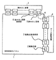
図1は発明に係る撮像装置としてのX線撮像装置の実施形態1を示す平面図、図2は図1中のA部分を拡大して示す平面図である。また、図3は図2のB−B’線における1画素の断面図、図4は図2のC−C’線における断面図、図5は図2のD−D’線における断面図、図6は図2のE−E’線における断面図である。各図面において、X線などの放射線を可視光に変換するシンチレータ層は、図示していない。
(Embodiment 1)
FIG. 1 is a plan view showing an embodiment 1 of an X-ray imaging apparatus as an imaging apparatus according to the invention, and FIG. 2 is an enlarged plan view showing a portion A in FIG. 3 is a cross-sectional view of one pixel taken along line BB ′ of FIG. 2, FIG. 4 is a cross-sectional view taken along line CC ′ of FIG. 2, and FIG. 5 is a cross-sectional view taken along line DD ′ of FIG. 6 is a cross-sectional view taken along line EE ′ of FIG. In each drawing, a scintillator layer for converting radiation such as X-rays into visible light is not shown.
X線撮像装置は、図1に示すようにセンサ基板としての放射線検出パネル1を有し、この放射線検出パネル1は駆動回路接続部3を介して外部回路である駆動回路2を有するゲート駆動装置4に接続されている。また読み出し回路接続部6を介して外部回路である読み出し回路5を有する読み出し装置7に接続されている。ゲート駆動装置4はスイッチ素子(TFT)のON、OFFを制御し、読み出し装置7はTFTからの信号を外部に読み出す。
As shown in FIG. 1, the X-ray imaging apparatus has a radiation detection panel 1 as a sensor substrate, and the radiation detection panel 1 has a drive circuit 2 that is an external circuit via a drive circuit connection unit 3. 4 is connected. Further, it is connected to a
次に、本実施形態の動作原理を図2を用いて説明する。図2の外部回路接続電極16は図1の読み出し回路接続部6に接続され、放射線検出パネル1の信号線やバイアス線等は外部回路接続電極16を介して図1の読み出し回路5に接続されている。 Next, the operation principle of this embodiment will be described with reference to FIG. The external circuit connection electrode 16 in FIG. 2 is connected to the readout circuit connection unit 6 in FIG. 1, and the signal lines and bias lines of the radiation detection panel 1 are connected to the readout circuit 5 in FIG. ing.
まず、変換素子であるMIS型光電変換素子10の光電変換層が空乏化するようにバイアス線(Vs線)11にバイアスが与えられる。例えば、信号線(Sig線)12に基準電位(GND)が、Vs線11に10Vが与えられる。この状態で、被検体に向けて曝射されたX線は、被検体により減衰を受けて透過し、図示しないシンチレータ層で可視光に変換され、この可視光が変換素子10に入射して電荷に変換される。
First, a bias is applied to the bias line (Vs line) 11 so that the photoelectric conversion layer of the MIS type
この電荷はゲート駆動装置4からゲート線(Vg線)13に印加されるゲート駆動パルスによりスイッチ素子(TFT)14を介してSig線12に転送され、読み出し装置7により外部に読み出される。その後、Vs線11の電位変化により変換素子10で発生し転送されなかった残留電荷が除去される。この時Vs線11は、例えば、10Vから−5Vに変化する。残留電荷の除去に関しては、TFTを用いて行ってもよい。
This electric charge is transferred to the
次に、図3を用いて放射線検出パネル1の層構成を説明する。MIS型光電変換素子10は、絶縁基板19上に、第1の電極層20、第1の絶縁層21、光電変換層である半導体層(a−Si層)22が順次形成されている。また、不純物半導体層23、Vs線11を形成する第2の電極層24、第3の電極層25が順次形成されている。第3の電極層25はVs線11から供給されるバイアス電圧を、MIS型光電変換素子10全体に印加するための電極を形成している。
Next, the layer configuration of the radiation detection panel 1 will be described with reference to FIG. In the MIS
TFT14は絶縁基板19上にゲート電極とVg線を形成する第1の電極層20、第1の絶縁層21、チャネル層である半導体層(a−Si層)22、不純物半導体層23、ソース又はドレイン電極とSig線を形成する第2の電極層24が順次形成されている。MIS型光電変換素子10及びTFT14の上層には、第2の絶縁層26、保護層27、接着層28、X線を可視光に波長変換するシンチレータ層29が順次形成されている。図3はMIS型光電変換素子10とTFT14を、同様の層で同時形成することにより製造プロセスの簡略化を図った例を示す。
The TFT 14 includes a first electrode layer 20 that forms a gate electrode and a Vg line on an insulating substrate 19, a first insulating layer 21, a semiconductor layer (a-Si layer) 22 that is a channel layer, an impurity semiconductor layer 23, a source or A second electrode layer 24 for forming a drain electrode and a Sig line is sequentially formed. A second insulating layer 26, a protective layer 27, an adhesive layer 28, and a scintillator layer 29 that converts the wavelength of X-rays into visible light are sequentially formed on the MIS
また、図4は上述のように図2のC−C’線における断面図であり、図2の引き出し線15の断面構造を示す。図4では図3と同一部分には同一符号を付している。図2と図4に示すように各配線(Sig線とVs線)と外部回路接続電極16を接続する引き出し配線15の構造は、Sig線12もVs線11も同様であり、第2の電極層24から形成されている。
4 is a cross-sectional view taken along line C-C ′ of FIG. 2 as described above, and shows a cross-sectional structure of the lead line 15 of FIG. 4, the same parts as those in FIG. 3 are denoted by the same reference numerals. As shown in FIGS. 2 and 4, the structure of the lead-out wiring 15 that connects each wiring (Sig line and Vs line) and the external circuit connection electrode 16 is the same for both the
図5は図2のD−D’線における断面図であり、外部回路接続電極16付近の断面構造を示す。図5では図3と同一部分には同一符号を付している。図2及び図5に示すように外部回路接続電極16は第2の電極層24及び第3の電極層25から形成され、その上部の第2の絶縁層26は除去された構成となる。 FIG. 5 is a cross-sectional view taken along line D-D ′ of FIG. 2 and shows a cross-sectional structure in the vicinity of the external circuit connection electrode 16. In FIG. 5, the same parts as those in FIG. As shown in FIGS. 2 and 5, the external circuit connection electrode 16 is formed of the second electrode layer 24 and the third electrode layer 25, and the second insulating layer 26 on the upper side thereof is removed.
本実施形態においては、引き出し配線15及び外部回路接続電極16の下層に不純物半導体層23、半導体層22、第1の絶縁層21を配置しているが、これらの層は必ずしも配置する必要はない。 In the present embodiment, the impurity semiconductor layer 23, the semiconductor layer 22, and the first insulating layer 21 are disposed below the lead-out wiring 15 and the external circuit connection electrode 16, but these layers are not necessarily disposed. .
ここで、従来の装置において画像ムラが生じる原因について考える。通常、保護層に含まれる極性溶媒は、熱による保護層の硬化工程で消失する。しかしながら、硬化条件によっては、極性溶媒が電荷若しくはイオンとして保護層中に残留する場合がある。この電荷若しくはイオンはVs線に加わる電圧によりVs線上部に集中し、電極の役割を持つことにより、近傍のSig線と容量を形成する。 Here, the cause of image unevenness in the conventional apparatus will be considered. Usually, the polar solvent contained in the protective layer disappears in the step of curing the protective layer with heat. However, depending on the curing conditions, the polar solvent may remain in the protective layer as charges or ions. The charges or ions are concentrated on the upper part of the Vs line due to the voltage applied to the Vs line, and form a capacitance with the nearby Sig line by acting as an electrode.
この容量は、Vs線に近い位置にあるSig線では大きく、Vs線から遠い位置にあるSig線では小さい。即ち、各Sig線には異なる容量が形成されるため、画像ムラが生じると考えられる。 This capacity is large for the Sig line located near the Vs line and small for the Sig line located far from the Vs line. That is, since different capacitances are formed in each Sig line, it is considered that image unevenness occurs.
図6は図2のE−E’線における断面図であり、Vs線11からVs接続電極配線17の断面構造を示す。図6では図3と同一部分には同一符号を付している。図2及び図6に示すように各Vs線11は保護層27の形成領域外において画素の近傍で第1の電極層20から形成されたVs接続配線17により共通化されている。Vs接続配線17は複数のSig線12と交差して配置されている。
FIG. 6 is a cross-sectional view taken along line E-E ′ of FIG. 2, and shows a cross-sectional structure from the
共通化されたVs線11は引き出し配線15により最端部の外部回路接続電極16に接続されている。またVs接続配線17は保護層27の形成領域外に配置され、この点が従来例と大きく異なる。
The
即ち、保護層27が形成された領域においてはVs線11とSig線12が交互に配置され、且つ、Vs線11とSig線12はそれぞれほぼ同一の間隔で配置されている。そのため、極性溶媒を用いた保護層27を配置した場合でも、各信号線の寄生容量はほぼ同等となり、画像ムラを低減することが可能となる。 That is, in the region where the protective layer 27 is formed, the Vs lines 11 and the Sig lines 12 are alternately arranged, and the Vs lines 11 and the Sig lines 12 are arranged at substantially the same intervals. Therefore, even when the protective layer 27 using a polar solvent is disposed, the parasitic capacitances of the signal lines are substantially equal, and image unevenness can be reduced.
ここで共通化されたVs線11の引き出し配線15(15aで示す引き出し配線)の配置例を次に示す。
(1)画素領域に対して一方の端部のみに配置する。
(2)画素領域に対して両端部に配置する。
(3)各読み出し回路接続部6の両端部に配置する。
これらの配置例において、いずれの配置も画像ムラを低減することができる。
An example of the arrangement of the lead-out wiring 15 (the lead-out wiring indicated by 15a) of the
(1) Arranged only at one end with respect to the pixel region.
(2) Arrange at both ends with respect to the pixel region.
(3) It arrange | positions at the both ends of each read-out circuit connection part 6. FIG.
In these arrangement examples, any arrangement can reduce image unevenness.
なお、図2には2×4画素を示しているが、実際には、例えば、2000×2000画素が配置され、センサ基板としての放射線検出パネルが構成されている。また、光電変換素子と、光電変換素子上に配置したシンチレータ層とを組み合わせた間接型の放射線検出パネルを示したが、本発明はこれに限るものではない。 Although FIG. 2 shows 2 × 4 pixels, actually, for example, 2000 × 2000 pixels are arranged, and a radiation detection panel as a sensor substrate is configured. Moreover, although the indirect type radiation detection panel which combined the photoelectric conversion element and the scintillator layer arrange | positioned on the photoelectric conversion element was shown, this invention is not limited to this.
例えば、光電変換素子に代えて、X線、γ線等の放射線を直接電荷に変換するアモルファスセレン等の半導体層を電極間に挟んだ変換素子を用いた直接型の放射線検出パネルにおいても同様の効果が得られる。 For example, instead of a photoelectric conversion element, the same applies to a direct radiation detection panel using a conversion element in which a semiconductor layer such as amorphous selenium that directly converts radiation such as X-rays and γ-rays into electric charges is sandwiched between electrodes. An effect is obtained.
また、間接型の放射線検出パネルの変換素子はMIS型光電変換素子とは別の光電変換素子、例えば、PIN型の光電変換素子を用いても構わない。更に、間接型の放射線検出パネルの画素構造に関しては、光電変換素子とスイッチ素子が同一層で構成された平面型でも、スイッチ素子の上部に光電変換素子が形成された積層型でも構わない。また、保護層27上に接着層28を介してシンチレータ層29を積層した例を示したが、保護層上に直接CsI等のシンチレータ層を設けてもよい。 Further, the conversion element of the indirect radiation detection panel may be a photoelectric conversion element different from the MIS photoelectric conversion element, for example, a PIN type photoelectric conversion element. Furthermore, the pixel structure of the indirect radiation detection panel may be a planar type in which the photoelectric conversion element and the switch element are formed of the same layer, or a stacked type in which the photoelectric conversion element is formed on the switch element. Moreover, although the example which laminated | stacked the scintillator layer 29 on the protective layer 27 via the contact bonding layer 28 was shown, you may provide scintillator layers, such as CsI, directly on a protective layer.
また、上述のようなX線を検知する撮像装置(X線撮像装置)を例に説明したが、γ線などの放射線を検知する撮像装置(放射線撮像装置)や、光を検出する撮像装置にも本発明を適用できる。 In addition, the imaging apparatus (X-ray imaging apparatus) that detects X-rays as described above has been described as an example. However, the imaging apparatus (radiation imaging apparatus) that detects radiation such as γ-rays or an imaging apparatus that detects light is used. The present invention can also be applied.
本発明は、入射する放射線を電気信号に変換するセンサ基板を有する撮像装置である。この撮像装置において、変換素子(MIS型光電変換素子)10と、変換素子に接続されたスイッチ素子(TFT)14とを有する複数の画素と、複数の画素上に配置された保護層27とを具備する。更に、変換素子に電気的に接続された複数のバイアス線(Vs線11)と、スイッチ素子に電気的に接続された複数の信号線(Sig線)12とを具備する。 The present invention is an imaging apparatus having a sensor substrate that converts incident radiation into an electrical signal. In this imaging apparatus, a plurality of pixels having a conversion element (MIS type photoelectric conversion element) 10 and a switch element (TFT) 14 connected to the conversion element, and a protective layer 27 disposed on the plurality of pixels are provided. It has. Furthermore, a plurality of bias lines (Vs lines 11) electrically connected to the conversion elements and a plurality of signal lines (Sig lines) 12 electrically connected to the switch elements are provided.
そして、本発明においては複数のバイアス線11の各々と複数の信号線12の各々は保護層27の領域内で所定間隔で交互に配置されている。そして、複数のバイアス線11は保護層27の領域外でVs接続配線17によって共通化され、且つ、Vs接続配線17は複数の信号線12と交差して配置されている。そのため、上述のように極性溶媒を用いた保護層27を配置した場合でも、各信号線の寄生容量はほぼ同等となり、画像ムラを低減することが可能となる。
In the present invention, each of the plurality of
(実施形態2)
次に、本発明の撮像装置の実施形態2について説明する。本実施形態の撮像装置の基本構成及び動作原理は実施形態1と同様であるため詳細な説明は省略する。図7は図1のA部分を拡大して示す平面図、図8は図7のF−F’線における断面図、図9は図7のG−G’における断面図である。図7〜図9では図2〜図6と同一部分には同一符号を付している。
(Embodiment 2)
Next, a second embodiment of the imaging apparatus of the present invention will be described. Since the basic configuration and operation principle of the imaging apparatus of the present embodiment are the same as those of the first embodiment, detailed description thereof is omitted. 7 is an enlarged plan view showing a portion A of FIG. 1, FIG. 8 is a cross-sectional view taken along line FF ′ of FIG. 7, and FIG. 9 is a cross-sectional view taken along line GG ′ of FIG. 7 to 9, the same parts as those in FIGS. 2 to 6 are denoted by the same reference numerals.
本実施形態において実施形態1と異なるのは、図7に示すようにVs接続配線17を引き出し配線15と外部回路接続電極16の間に配置した点である。その他の構成は実施形態1と同様である。 The present embodiment is different from the first embodiment in that the Vs connection wiring 17 is arranged between the lead wiring 15 and the external circuit connection electrode 16 as shown in FIG. Other configurations are the same as those of the first embodiment.
図8は図7のF−F’線における断面図であり、図7の引き出し線15の断面構造を示す。図7及び図8に示すようにSig線12と外部回路接続電極16を接続する引き出し配線15は第2の電極層24から形成され、Vs線11と外部回路接続電極16を接続する引き出し配線15は第1の電極層20から形成されている。
FIG. 8 is a cross-sectional view taken along the line F-F ′ of FIG. 7 and shows a cross-sectional structure of the lead line 15 of FIG. 7. As shown in FIGS. 7 and 8, the lead-out wiring 15 that connects the
つまり、複数のバイアス線(Vs線11)を外部回路接続電極16に引き出す引き出し配線15と、複数の信号線(Sig線12)を外部回路接続電極16に引き出す引き出し配線15とは、異なる金属層で形成されている。このように引き出し配線15を異なる層で形成することにより、引き出し配線15のピッチが小さい場合でも、全てのSig線12とVs線11を形成することが可能となる。 In other words, the lead-out wiring 15 that leads out the plurality of bias lines (Vs lines 11) to the external circuit connection electrode 16 and the lead-out wiring 15 that leads out the plurality of signal lines (Sig lines 12) to the external circuit connection electrode 16 are different metal layers. It is formed with. By forming the lead wirings 15 in different layers in this way, all the Sig lines 12 and the Vs lines 11 can be formed even when the pitch of the lead wirings 15 is small.
図9は図7のG−G’における断面図であり、図7のVs接続配線17から外部回路接続電極16付近の断面構造を示す。図7及び図9に示すように各Vs線11は外部回路接続電極16の近傍において第1の電極層20から形成されたVs接続配線17により共通化されている。Vs接続配線17は複数のSig線12と交差して配置されている。共通化されたVs線11は最端部の外部回路接続電極16に接続されている。更にVs接続配線17は保護層27の形成領域外に配置されている。
FIG. 9 is a cross-sectional view taken along the line G-G ′ of FIG. 7 and shows a cross-sectional structure in the vicinity of the external circuit connection electrode 16 from the Vs connection wiring 17 of FIG. 7. As shown in FIGS. 7 and 9, each
即ち、保護層27が形成された領域においては、実施形態1と同様にVs線11とSig線12が交互に配置され、Vs線11とSig線12がそれぞれほぼ同一の間隔で配置されている。そのため、極性溶媒を用いた保護層を配置した場合でも、各信号線の寄生容量はほぼ同等となり、画像ムラを低減することが可能となる。 That is, in the region where the protective layer 27 is formed, the Vs lines 11 and the Sig lines 12 are alternately arranged as in the first embodiment, and the Vs lines 11 and the Sig lines 12 are arranged at substantially the same intervals. . Therefore, even when a protective layer using a polar solvent is disposed, the parasitic capacitances of the signal lines are almost equal, and image unevenness can be reduced.
また、図9に示すように外部回路接続電極16は、第2の電極層24及び第3の電極層25から形成される。その上部の第2の絶縁層26は、外部回路が接続される部分のみ除去された構成となり、この点が実施形態1と異なる。本実施形態では、引き出し配線15及び外部回路接続電極16の下層に不純物半導体層23、半導体層22、第1の絶縁層21を配置しているが、これらの層は必ずしも配置する必要はない。 Further, as shown in FIG. 9, the external circuit connection electrode 16 is formed of a second electrode layer 24 and a third electrode layer 25. The upper second insulating layer 26 has a configuration in which only a portion to which an external circuit is connected is removed, which is different from the first embodiment. In this embodiment, the impurity semiconductor layer 23, the semiconductor layer 22, and the first insulating layer 21 are disposed below the lead-out wiring 15 and the external circuit connection electrode 16, but these layers are not necessarily disposed.
(実施形態3)
図10は本発明に係る撮像装置としての放射線撮像装置を用いた放射線撮像システムの一実施形態としてのX線診断システムを示す。
(Embodiment 3)
FIG. 10 shows an X-ray diagnostic system as an embodiment of a radiation imaging system using a radiation imaging apparatus as an imaging apparatus according to the present invention.
図10に示すように放射線源であるX線チューブ6050で発生したX線6060は患者或いは被験者6061の胸部6062を透過し、放射線画像を撮影する放射線撮像装置6040に入射する。この入射したX線には患者6061の体内部の情報が含まれている。X線の入射に対応して放射線撮像装置のシンチレータ層が発光し、これを光電変換して電気的情報が得られる。
As shown in FIG. 10,
この電気的情報は信号処理手段によって処理される。即ち、この情報はディジタル変換され、イメージプロセッサ6070により画像処理され、コントロールルームにある表示手段としてのディスプレイ6080で観察できる。
This electrical information is processed by signal processing means. That is, this information is digitally converted, subjected to image processing by the image processor 6070, and can be observed on a
また、この情報は通信回線6090等の伝送処理手段により遠隔地へ転送でき、別の場所のドクタールーム等で表示手段であるディスプレイ6081に表示するか、又は光ディスク等の記録手段に保存することができる。これにより、遠隔地の医師が診断することも可能である。また記録手段であるフィルムプロセッサ6100によりフィルム6110に記録することもできる。
Further, this information can be transferred to a remote place by transmission processing means such as a communication line 6090, and can be displayed on a display 6081 as a display means in a doctor room or the like in another place, or stored in a recording means such as an optical disk. it can. As a result, it is possible for a remote doctor to make a diagnosis. Moreover, it can also record on the
1 放射線検出パネル
2 駆動回路
4 ゲート駆動回路
5 読み出し回路
7 読み出し装置
10 MIS型光電変換素子
11 Vs配線
12 Sig線
13 Vg線
14 TFT
15 引き出し配線
16 外部回路接続電極
17 Vs接続配線
19 絶縁基板
20 第1の電極層
21 第1の絶縁層
22 半導体層
23 不純物半導体層
24 第2の電極層
25 第3の電極層
26 第2の絶縁層
27 保護層
28 接着層
29 シンチレータ層
DESCRIPTION OF SYMBOLS 1 Radiation detection panel 2 Drive circuit 4 Gate drive circuit 5 Read-out
DESCRIPTION OF SYMBOLS 15 Lead wiring 16 External circuit connection electrode 17 Vs connection wiring 19 Insulating substrate 20 1st electrode layer 21 1st insulating layer 22 Semiconductor layer 23 Impurity semiconductor layer 24 2nd electrode layer 25 3rd electrode layer 26 2nd Insulating layer 27 Protective layer 28 Adhesive layer 29 Scintillator layer
Claims (4)
前記センサ基板は、
変換素子と、前記変換素子に接続されたスイッチ素子とを有する複数の画素と、
前記複数の画素上に配置された保護層と、
前記変換素子に電気的に接続された複数のバイアス線と、
前記スイッチ素子に電気的に接続された複数の信号線とを有し、
前記複数のバイアス線の各々と前記複数の信号線の各々は前記保護層の領域内で所定間隔で交互に配置され、
前記複数のバイアス線は前記保護層の領域外で接続配線によって共通化され、且つ、前記接続配線は前記複数の信号線と交差して配置されていることを特徴とする撮像装置。 In an imaging apparatus having a sensor substrate that converts incident radiation into an electrical signal,
The sensor substrate is
A plurality of pixels having a conversion element and a switch element connected to the conversion element;
A protective layer disposed on the plurality of pixels;
A plurality of bias lines electrically connected to the conversion element;
A plurality of signal lines electrically connected to the switch element;
Each of the plurality of bias lines and each of the plurality of signal lines are alternately arranged at predetermined intervals in the region of the protective layer,
The image pickup apparatus, wherein the plurality of bias lines are shared by a connection wiring outside the region of the protective layer, and the connection wiring is arranged so as to intersect the plurality of signal lines.
前記撮像装置からの信号を処理する信号処理手段と、
前記信号処理手段からの信号を記録するための記録手段と、
前記信号処理手段からの信号を表示するための表示手段と、
前記信号処理手段からの信号を伝送するための伝送処理手段と、
前記放射線を発生させるための放射線源と、を具備することを特徴とする放射線撮像システム。 The imaging device according to any one of claims 1 to 3,
Signal processing means for processing a signal from the imaging device;
Recording means for recording a signal from the signal processing means;
Display means for displaying a signal from the signal processing means;
Transmission processing means for transmitting a signal from the signal processing means;
A radiation imaging system comprising: a radiation source for generating the radiation.
Priority Applications (2)
| Application Number | Priority Date | Filing Date | Title |
|---|---|---|---|
| JP2007205472A JP5235350B2 (en) | 2007-08-07 | 2007-08-07 | Imaging apparatus and radiation imaging system |
| US12/185,445 US7932946B2 (en) | 2007-08-07 | 2008-08-04 | Imaging apparatus and radiation imaging system |
Applications Claiming Priority (1)
| Application Number | Priority Date | Filing Date | Title |
|---|---|---|---|
| JP2007205472A JP5235350B2 (en) | 2007-08-07 | 2007-08-07 | Imaging apparatus and radiation imaging system |
Publications (3)
| Publication Number | Publication Date |
|---|---|
| JP2009043826A true JP2009043826A (en) | 2009-02-26 |
| JP2009043826A5 JP2009043826A5 (en) | 2010-08-19 |
| JP5235350B2 JP5235350B2 (en) | 2013-07-10 |
Family
ID=40346102
Family Applications (1)
| Application Number | Title | Priority Date | Filing Date |
|---|---|---|---|
| JP2007205472A Active JP5235350B2 (en) | 2007-08-07 | 2007-08-07 | Imaging apparatus and radiation imaging system |
Country Status (2)
| Country | Link |
|---|---|
| US (1) | US7932946B2 (en) |
| JP (1) | JP5235350B2 (en) |
Cited By (2)
| Publication number | Priority date | Publication date | Assignee | Title |
|---|---|---|---|---|
| WO2016104339A1 (en) * | 2014-12-25 | 2016-06-30 | シャープ株式会社 | Photosensor substrate and method for producing same |
| WO2016195000A1 (en) * | 2015-06-04 | 2016-12-08 | シャープ株式会社 | Photosensor substrate |
Families Citing this family (20)
| Publication number | Priority date | Publication date | Assignee | Title |
|---|---|---|---|---|
| JP5196739B2 (en) | 2006-06-09 | 2013-05-15 | キヤノン株式会社 | Radiation imaging apparatus and radiation imaging system |
| JP5489542B2 (en) * | 2008-07-01 | 2014-05-14 | キヤノン株式会社 | Radiation detection apparatus and radiation imaging system |
| JP5439837B2 (en) | 2009-02-10 | 2014-03-12 | ソニー株式会社 | Display device |
| JP6057511B2 (en) | 2011-12-21 | 2017-01-11 | キヤノン株式会社 | Imaging apparatus and radiation imaging system |
| JP5954983B2 (en) | 2011-12-21 | 2016-07-20 | キヤノン株式会社 | Imaging apparatus, radiation imaging system, and manufacturing method of imaging apparatus |
| JP6585910B2 (en) | 2014-05-01 | 2019-10-02 | キヤノン株式会社 | Radiation imaging apparatus and radiation imaging system |
| JP6480670B2 (en) | 2014-05-01 | 2019-03-13 | キヤノン株式会社 | Radiation imaging apparatus and radiation imaging system |
| JP6570315B2 (en) | 2015-05-22 | 2019-09-04 | キヤノン株式会社 | Radiation imaging apparatus and radiation imaging system |
| JP6929104B2 (en) | 2017-04-05 | 2021-09-01 | キヤノン株式会社 | Radiation imaging device, radiation imaging system, control method and program of radiation imaging device |
| JP6928746B2 (en) * | 2017-04-10 | 2021-09-01 | ブリルニクス シンガポール プライベート リミテッド | Solid-state image sensor, manufacturing method of solid-state image sensor, and electronic equipment |
| JP6990986B2 (en) | 2017-04-27 | 2022-01-12 | キヤノン株式会社 | Radiation imaging device, radiation imaging system, control method and program of radiation imaging device |
| JP6853729B2 (en) | 2017-05-08 | 2021-03-31 | キヤノン株式会社 | Radiation imaging device, radiation imaging system, control method and program of radiation imaging device |
| JP6788547B2 (en) * | 2017-05-09 | 2020-11-25 | キヤノン株式会社 | Radiation imaging device, its control method, control device, and radiation imaging system |
| JP6877289B2 (en) | 2017-07-31 | 2021-05-26 | キヤノン株式会社 | Manufacturing method of radiation detection device, radiation detection system, and radiation emission device |
| JP7045834B2 (en) | 2017-11-10 | 2022-04-01 | キヤノン株式会社 | Radiation imaging system |
| JP7079113B2 (en) | 2018-02-21 | 2022-06-01 | キヤノン株式会社 | Radiation imaging device and radiation imaging system |
| JP7198003B2 (en) | 2018-06-22 | 2022-12-28 | キヤノン株式会社 | Radiation Imaging Apparatus, Radiation Imaging System, Radiation Imaging Apparatus Control Method and Program |
| JP6659182B2 (en) | 2018-07-23 | 2020-03-04 | キヤノン株式会社 | Radiation imaging apparatus, manufacturing method thereof, and radiation imaging system |
| EP3661190A1 (en) | 2018-11-27 | 2020-06-03 | Canon Kabushiki Kaisha | Radiation imaging apparatus and radiation imaging system |
| JP7397635B2 (en) | 2019-11-22 | 2023-12-13 | キヤノン株式会社 | Radiation detection device, radiation detection system, control method and program |
Citations (4)
| Publication number | Priority date | Publication date | Assignee | Title |
|---|---|---|---|---|
| JP2003270351A (en) * | 2002-03-12 | 2003-09-25 | Canon Inc | Radiography device |
| JP2004184273A (en) * | 2002-12-04 | 2004-07-02 | Casio Comput Co Ltd | Method for inspecting device |
| JP2006189377A (en) * | 2005-01-07 | 2006-07-20 | Canon Inc | Scintillator panel, radiation detector, and radiation detection system |
| JP2007049123A (en) * | 2005-07-11 | 2007-02-22 | Canon Inc | Conversion apparatus, radiation detector, and radiation detecting system |
Family Cites Families (5)
| Publication number | Priority date | Publication date | Assignee | Title |
|---|---|---|---|---|
| JP2002050754A (en) * | 2000-05-08 | 2002-02-15 | Canon Inc | Semiconductor device, production method therefor, radiation detector and radiation detecting system using the same |
| JP2004325261A (en) * | 2003-04-24 | 2004-11-18 | Canon Inc | Radiation image imaging apparatus |
| JP4845352B2 (en) * | 2004-06-15 | 2011-12-28 | キヤノン株式会社 | Radiation imaging apparatus, manufacturing method thereof, and radiation imaging system |
| JP4908947B2 (en) * | 2005-07-11 | 2012-04-04 | キヤノン株式会社 | Conversion device, radiation detection device, and radiation detection system |
| JP5173234B2 (en) * | 2006-05-24 | 2013-04-03 | キヤノン株式会社 | Radiation imaging apparatus and radiation imaging system |
-
2007
- 2007-08-07 JP JP2007205472A patent/JP5235350B2/en active Active
-
2008
- 2008-08-04 US US12/185,445 patent/US7932946B2/en not_active Expired - Fee Related
Patent Citations (4)
| Publication number | Priority date | Publication date | Assignee | Title |
|---|---|---|---|---|
| JP2003270351A (en) * | 2002-03-12 | 2003-09-25 | Canon Inc | Radiography device |
| JP2004184273A (en) * | 2002-12-04 | 2004-07-02 | Casio Comput Co Ltd | Method for inspecting device |
| JP2006189377A (en) * | 2005-01-07 | 2006-07-20 | Canon Inc | Scintillator panel, radiation detector, and radiation detection system |
| JP2007049123A (en) * | 2005-07-11 | 2007-02-22 | Canon Inc | Conversion apparatus, radiation detector, and radiation detecting system |
Cited By (3)
| Publication number | Priority date | Publication date | Assignee | Title |
|---|---|---|---|---|
| WO2016104339A1 (en) * | 2014-12-25 | 2016-06-30 | シャープ株式会社 | Photosensor substrate and method for producing same |
| WO2016195000A1 (en) * | 2015-06-04 | 2016-12-08 | シャープ株式会社 | Photosensor substrate |
| US10276611B2 (en) | 2015-06-04 | 2019-04-30 | Sharp Kabushiki Kaisha | Photosensor substrate |
Also Published As
| Publication number | Publication date |
|---|---|
| US20090040348A1 (en) | 2009-02-12 |
| JP5235350B2 (en) | 2013-07-10 |
| US7932946B2 (en) | 2011-04-26 |
Similar Documents
| Publication | Publication Date | Title |
|---|---|---|
| JP5235350B2 (en) | Imaging apparatus and radiation imaging system | |
| JP6442163B2 (en) | Radiation imaging apparatus and radiation imaging system | |
| US8067743B2 (en) | Imaging apparatus and radiation imaging apparatus | |
| JP6480670B2 (en) | Radiation imaging apparatus and radiation imaging system | |
| JP5159065B2 (en) | Radiation detection apparatus, radiation imaging apparatus, and radiation imaging system | |
| JP5043373B2 (en) | Conversion device, radiation detection device, and radiation detection system | |
| JP4750512B2 (en) | Radiation imaging apparatus, control method therefor, and radiation imaging system | |
| JP4845352B2 (en) | Radiation imaging apparatus, manufacturing method thereof, and radiation imaging system | |
| JP4908947B2 (en) | Conversion device, radiation detection device, and radiation detection system | |
| JP5328169B2 (en) | Imaging apparatus and radiation imaging system | |
| JP2007049124A (en) | Conversion apparatus, radiation detector, and radiation detecting system | |
| JP5700973B2 (en) | Detection apparatus and radiation detection system | |
| JP5400507B2 (en) | Imaging apparatus and radiation imaging system | |
| JP4067055B2 (en) | Imaging apparatus and manufacturing method thereof, radiation imaging apparatus, and radiation imaging system | |
| JP2012079860A (en) | Detector and radiation detection system | |
| JP2008141705A (en) | Radiation imaging apparatus and system | |
| JP2012129425A (en) | Matrix substrate, detection apparatus, detection system and detection apparatus driving method | |
| JP2012079820A (en) | Detector and radiation detection system | |
| JP6470508B2 (en) | Radiation imaging apparatus and radiation imaging system | |
| JP5677353B2 (en) | Radiation detection apparatus and radiation imaging system | |
| JP2016201665A (en) | Radiographic apparatus and radiographic system | |
| JP2016109631A (en) | Radiation imaging device and radiation imaging system | |
| JP2006005150A (en) | Imaging device and radiographic imaging device and radiographic imaging system | |
| JP2004303925A (en) | Substrate for imaging | |
| JP6436754B2 (en) | Radiation imaging apparatus and radiation imaging system |
Legal Events
| Date | Code | Title | Description |
|---|---|---|---|
| RD03 | Notification of appointment of power of attorney |
Free format text: JAPANESE INTERMEDIATE CODE: A7423 Effective date: 20090326 |
|
| RD05 | Notification of revocation of power of attorney |
Free format text: JAPANESE INTERMEDIATE CODE: A7425 Effective date: 20090427 |
|
| A521 | Request for written amendment filed |
Free format text: JAPANESE INTERMEDIATE CODE: A523 Effective date: 20100630 |
|
| A621 | Written request for application examination |
Free format text: JAPANESE INTERMEDIATE CODE: A621 Effective date: 20100630 |
|
| A977 | Report on retrieval |
Free format text: JAPANESE INTERMEDIATE CODE: A971007 Effective date: 20120912 |
|
| A131 | Notification of reasons for refusal |
Free format text: JAPANESE INTERMEDIATE CODE: A131 Effective date: 20120921 |
|
| A521 | Request for written amendment filed |
Free format text: JAPANESE INTERMEDIATE CODE: A523 Effective date: 20121114 |
|
| A131 | Notification of reasons for refusal |
Free format text: JAPANESE INTERMEDIATE CODE: A131 Effective date: 20121207 |
|
| A521 | Request for written amendment filed |
Free format text: JAPANESE INTERMEDIATE CODE: A523 Effective date: 20130205 |
|
| TRDD | Decision of grant or rejection written | ||
| A01 | Written decision to grant a patent or to grant a registration (utility model) |
Free format text: JAPANESE INTERMEDIATE CODE: A01 Effective date: 20130225 |
|
| A61 | First payment of annual fees (during grant procedure) |
Free format text: JAPANESE INTERMEDIATE CODE: A61 Effective date: 20130326 |
|
| R151 | Written notification of patent or utility model registration |
Ref document number: 5235350 Country of ref document: JP Free format text: JAPANESE INTERMEDIATE CODE: R151 |
|
| FPAY | Renewal fee payment (event date is renewal date of database) |
Free format text: PAYMENT UNTIL: 20160405 Year of fee payment: 3 |