JP4908947B2 - Conversion device, radiation detection device, and radiation detection system - Google Patents
Conversion device, radiation detection device, and radiation detection system Download PDFInfo
- Publication number
- JP4908947B2 JP4908947B2 JP2006181890A JP2006181890A JP4908947B2 JP 4908947 B2 JP4908947 B2 JP 4908947B2 JP 2006181890 A JP2006181890 A JP 2006181890A JP 2006181890 A JP2006181890 A JP 2006181890A JP 4908947 B2 JP4908947 B2 JP 4908947B2
- Authority
- JP
- Japan
- Prior art keywords
- wiring
- layer
- terminal
- signal
- radiation detection
- Prior art date
- Legal status (The legal status is an assumption and is not a legal conclusion. Google has not performed a legal analysis and makes no representation as to the accuracy of the status listed.)
- Expired - Fee Related
Links
- 238000006243 chemical reaction Methods 0.000 title claims description 57
- 230000005855 radiation Effects 0.000 title claims description 44
- 238000001514 detection method Methods 0.000 title claims description 30
- 239000010410 layer Substances 0.000 claims description 129
- 239000002184 metal Substances 0.000 claims description 55
- 239000000758 substrate Substances 0.000 claims description 39
- 239000011241 protective layer Substances 0.000 claims description 25
- 239000004065 semiconductor Substances 0.000 claims description 25
- 238000012545 processing Methods 0.000 claims description 15
- 238000000034 method Methods 0.000 claims description 10
- 239000000463 material Substances 0.000 claims description 6
- 229910002064 alloy oxide Inorganic materials 0.000 claims description 4
- 230000005540 biological transmission Effects 0.000 claims description 2
- 239000000956 alloy Substances 0.000 claims 1
- 229910045601 alloy Inorganic materials 0.000 claims 1
- 239000012535 impurity Substances 0.000 description 19
- 238000003384 imaging method Methods 0.000 description 14
- 229910021417 amorphous silicon Inorganic materials 0.000 description 9
- 230000007797 corrosion Effects 0.000 description 8
- 238000005260 corrosion Methods 0.000 description 8
- 239000010408 film Substances 0.000 description 7
- 238000011109 contamination Methods 0.000 description 6
- 239000011159 matrix material Substances 0.000 description 6
- OAICVXFJPJFONN-UHFFFAOYSA-N Phosphorus Chemical compound [P] OAICVXFJPJFONN-UHFFFAOYSA-N 0.000 description 5
- 238000005530 etching Methods 0.000 description 5
- ORQBXQOJMQIAOY-UHFFFAOYSA-N nobelium Chemical compound [No] ORQBXQOJMQIAOY-UHFFFAOYSA-N 0.000 description 5
- 238000010438 heat treatment Methods 0.000 description 4
- 230000007423 decrease Effects 0.000 description 3
- 238000003745 diagnosis Methods 0.000 description 3
- 239000011229 interlayer Substances 0.000 description 3
- 238000004519 manufacturing process Methods 0.000 description 3
- 238000007789 sealing Methods 0.000 description 3
- 239000000853 adhesive Substances 0.000 description 2
- 230000001070 adhesive effect Effects 0.000 description 2
- 239000013078 crystal Substances 0.000 description 2
- 238000009413 insulation Methods 0.000 description 2
- 239000007769 metal material Substances 0.000 description 2
- 238000012546 transfer Methods 0.000 description 2
- 229910004613 CdTe Inorganic materials 0.000 description 1
- LFQSCWFLJHTTHZ-UHFFFAOYSA-N Ethanol Chemical compound CCO LFQSCWFLJHTTHZ-UHFFFAOYSA-N 0.000 description 1
- 238000004140 cleaning Methods 0.000 description 1
- 230000007547 defect Effects 0.000 description 1
- 238000011161 development Methods 0.000 description 1
- 238000002059 diagnostic imaging Methods 0.000 description 1
- 238000010586 diagram Methods 0.000 description 1
- 238000001035 drying Methods 0.000 description 1
- 239000011521 glass Substances 0.000 description 1
- 238000007689 inspection Methods 0.000 description 1
- CNQCVBJFEGMYDW-UHFFFAOYSA-N lawrencium atom Chemical compound [Lr] CNQCVBJFEGMYDW-UHFFFAOYSA-N 0.000 description 1
- 238000009659 non-destructive testing Methods 0.000 description 1
- 230000003287 optical effect Effects 0.000 description 1
- 230000002093 peripheral effect Effects 0.000 description 1
- 229910021420 polycrystalline silicon Inorganic materials 0.000 description 1
- 239000010453 quartz Substances 0.000 description 1
- 238000002601 radiography Methods 0.000 description 1
- 230000035945 sensitivity Effects 0.000 description 1
- VYPSYNLAJGMNEJ-UHFFFAOYSA-N silicon dioxide Inorganic materials O=[Si]=O VYPSYNLAJGMNEJ-UHFFFAOYSA-N 0.000 description 1
- 230000001954 sterilising effect Effects 0.000 description 1
- 238000004659 sterilization and disinfection Methods 0.000 description 1
- 238000003860 storage Methods 0.000 description 1
- 239000000126 substance Substances 0.000 description 1
- 239000010409 thin film Substances 0.000 description 1
- 230000000007 visual effect Effects 0.000 description 1
Images


Classifications
-
- H—ELECTRICITY
- H01—ELECTRIC ELEMENTS
- H01L—SEMICONDUCTOR DEVICES NOT COVERED BY CLASS H10
- H01L27/00—Devices consisting of a plurality of semiconductor or other solid-state components formed in or on a common substrate
- H01L27/14—Devices consisting of a plurality of semiconductor or other solid-state components formed in or on a common substrate including semiconductor components sensitive to infrared radiation, light, electromagnetic radiation of shorter wavelength or corpuscular radiation and specially adapted either for the conversion of the energy of such radiation into electrical energy or for the control of electrical energy by such radiation
- H01L27/144—Devices controlled by radiation
- H01L27/146—Imager structures
- H01L27/14601—Structural or functional details thereof
- H01L27/14603—Special geometry or disposition of pixel-elements, address-lines or gate-electrodes
-
- G—PHYSICS
- G01—MEASURING; TESTING
- G01T—MEASUREMENT OF NUCLEAR OR X-RADIATION
- G01T1/00—Measuring X-radiation, gamma radiation, corpuscular radiation, or cosmic radiation
- G01T1/29—Measurement performed on radiation beams, e.g. position or section of the beam; Measurement of spatial distribution of radiation
- G01T1/2914—Measurement of spatial distribution of radiation
- G01T1/2921—Static instruments for imaging the distribution of radioactivity in one or two dimensions; Radio-isotope cameras
- G01T1/2928—Static instruments for imaging the distribution of radioactivity in one or two dimensions; Radio-isotope cameras using solid state detectors
-
- H—ELECTRICITY
- H01—ELECTRIC ELEMENTS
- H01L—SEMICONDUCTOR DEVICES NOT COVERED BY CLASS H10
- H01L27/00—Devices consisting of a plurality of semiconductor or other solid-state components formed in or on a common substrate
- H01L27/14—Devices consisting of a plurality of semiconductor or other solid-state components formed in or on a common substrate including semiconductor components sensitive to infrared radiation, light, electromagnetic radiation of shorter wavelength or corpuscular radiation and specially adapted either for the conversion of the energy of such radiation into electrical energy or for the control of electrical energy by such radiation
- H01L27/144—Devices controlled by radiation
- H01L27/146—Imager structures
- H01L27/14601—Structural or functional details thereof
- H01L27/14632—Wafer-level processed structures
-
- H—ELECTRICITY
- H01—ELECTRIC ELEMENTS
- H01L—SEMICONDUCTOR DEVICES NOT COVERED BY CLASS H10
- H01L27/00—Devices consisting of a plurality of semiconductor or other solid-state components formed in or on a common substrate
- H01L27/14—Devices consisting of a plurality of semiconductor or other solid-state components formed in or on a common substrate including semiconductor components sensitive to infrared radiation, light, electromagnetic radiation of shorter wavelength or corpuscular radiation and specially adapted either for the conversion of the energy of such radiation into electrical energy or for the control of electrical energy by such radiation
- H01L27/144—Devices controlled by radiation
- H01L27/146—Imager structures
- H01L27/14643—Photodiode arrays; MOS imagers
- H01L27/14658—X-ray, gamma-ray or corpuscular radiation imagers
- H01L27/14663—Indirect radiation imagers, e.g. using luminescent members
-
- H—ELECTRICITY
- H01—ELECTRIC ELEMENTS
- H01L—SEMICONDUCTOR DEVICES NOT COVERED BY CLASS H10
- H01L31/00—Semiconductor devices sensitive to infrared radiation, light, electromagnetic radiation of shorter wavelength or corpuscular radiation and specially adapted either for the conversion of the energy of such radiation into electrical energy or for the control of electrical energy by such radiation; Processes or apparatus specially adapted for the manufacture or treatment thereof or of parts thereof; Details thereof
- H01L31/08—Semiconductor devices sensitive to infrared radiation, light, electromagnetic radiation of shorter wavelength or corpuscular radiation and specially adapted either for the conversion of the energy of such radiation into electrical energy or for the control of electrical energy by such radiation; Processes or apparatus specially adapted for the manufacture or treatment thereof or of parts thereof; Details thereof in which radiation controls flow of current through the device, e.g. photoresistors
- H01L31/10—Semiconductor devices sensitive to infrared radiation, light, electromagnetic radiation of shorter wavelength or corpuscular radiation and specially adapted either for the conversion of the energy of such radiation into electrical energy or for the control of electrical energy by such radiation; Processes or apparatus specially adapted for the manufacture or treatment thereof or of parts thereof; Details thereof in which radiation controls flow of current through the device, e.g. photoresistors characterised by potential barriers, e.g. phototransistors
- H01L31/101—Devices sensitive to infrared, visible or ultraviolet radiation
- H01L31/112—Devices sensitive to infrared, visible or ultraviolet radiation characterised by field-effect operation, e.g. junction field-effect phototransistor
- H01L31/113—Devices sensitive to infrared, visible or ultraviolet radiation characterised by field-effect operation, e.g. junction field-effect phototransistor being of the conductor-insulator-semiconductor type, e.g. metal-insulator-semiconductor field-effect transistor
- H01L31/1136—Devices sensitive to infrared, visible or ultraviolet radiation characterised by field-effect operation, e.g. junction field-effect phototransistor being of the conductor-insulator-semiconductor type, e.g. metal-insulator-semiconductor field-effect transistor the device being a metal-insulator-semiconductor field-effect transistor
-
- H—ELECTRICITY
- H01—ELECTRIC ELEMENTS
- H01L—SEMICONDUCTOR DEVICES NOT COVERED BY CLASS H10
- H01L27/00—Devices consisting of a plurality of semiconductor or other solid-state components formed in or on a common substrate
- H01L27/02—Devices consisting of a plurality of semiconductor or other solid-state components formed in or on a common substrate including semiconductor components specially adapted for rectifying, oscillating, amplifying or switching and having potential barriers; including integrated passive circuit elements having potential barriers
- H01L27/12—Devices consisting of a plurality of semiconductor or other solid-state components formed in or on a common substrate including semiconductor components specially adapted for rectifying, oscillating, amplifying or switching and having potential barriers; including integrated passive circuit elements having potential barriers the substrate being other than a semiconductor body, e.g. an insulating body
- H01L27/1214—Devices consisting of a plurality of semiconductor or other solid-state components formed in or on a common substrate including semiconductor components specially adapted for rectifying, oscillating, amplifying or switching and having potential barriers; including integrated passive circuit elements having potential barriers the substrate being other than a semiconductor body, e.g. an insulating body comprising a plurality of TFTs formed on a non-semiconducting substrate, e.g. driving circuits for AMLCDs
- H01L27/124—Devices consisting of a plurality of semiconductor or other solid-state components formed in or on a common substrate including semiconductor components specially adapted for rectifying, oscillating, amplifying or switching and having potential barriers; including integrated passive circuit elements having potential barriers the substrate being other than a semiconductor body, e.g. an insulating body comprising a plurality of TFTs formed on a non-semiconducting substrate, e.g. driving circuits for AMLCDs with a particular composition, shape or layout of the wiring layers specially adapted to the circuit arrangement, e.g. scanning lines in LCD pixel circuits
Landscapes
- Physics & Mathematics (AREA)
- Engineering & Computer Science (AREA)
- Power Engineering (AREA)
- General Physics & Mathematics (AREA)
- Computer Hardware Design (AREA)
- Electromagnetism (AREA)
- Condensed Matter Physics & Semiconductors (AREA)
- Microelectronics & Electronic Packaging (AREA)
- Health & Medical Sciences (AREA)
- Molecular Biology (AREA)
- Spectroscopy & Molecular Physics (AREA)
- Toxicology (AREA)
- High Energy & Nuclear Physics (AREA)
- Life Sciences & Earth Sciences (AREA)
- Solid State Image Pick-Up Elements (AREA)
- Transforming Light Signals Into Electric Signals (AREA)
- Measurement Of Radiation (AREA)
Description
本発明は、医療用画像診断装置、非破壊検査装置、放射線を用いた分析装置などに応用される光電変換用基板及び光電変換装置、放射線検出用基板及び放射線検出装置に関するものである。なお、本明細書では、可視光等の電磁波やX線、α線、β線、γ線なども、放射線に含まれるものとする。 The present invention relates to a photoelectric conversion substrate and a photoelectric conversion device, a radiation detection substrate, and a radiation detection device that are applied to a medical diagnostic imaging device, a nondestructive inspection device, an analysis device using radiation, and the like. In this specification, electromagnetic waves such as visible light, X-rays, α-rays, β-rays, γ-rays, and the like are also included in the radiation.
従来、医療画像診断で用いられる撮影としては、レントゲン撮影などの静止画像を取得する一般撮影と、動画像を取得する透視撮影とに分類される。それぞれの撮影は、必要に応じて撮像装置を含めて選択される。 Conventionally, imaging used for medical image diagnosis is classified into general imaging for acquiring a still image such as X-ray imaging and fluoroscopic imaging for acquiring a moving image. Each photographing is selected including an imaging device as necessary.
従来の一般撮影においては、主に以下に示す2つの方式により行われていた。ひとつは蛍光板とフィルムを組み合わせたスクリーンフィルムを用いてフィルムの露光、現像、及び定着により撮影するスクリーンフィルム撮影(以下SF撮影と略記する)方式である。もうひとつは、放射線画像を輝尽性蛍光体に潜像として記録し、その輝尽性蛍光体にレーザを走査して潜像に応じた光情報を出力し、出力された光情報をセンサで読み取るコンピューティドラジオグラフィ撮影(以下CR撮影と略記する)方式である。しかしながら、従来の一般撮影では、放射線画像を取得するための工程が煩雑であるといった課題があった。また、取得された放射線画像をデジタルデータとすることは可能であるが、間接的にデジタル化することとなり、デジタル化された放射線画像データを取得するまでに多くの時間を必要とするといった課題もあった。 Conventional general photography is mainly performed by the following two methods. One is a screen film photographing (hereinafter abbreviated as SF photographing) method in which a screen film in which a fluorescent plate and a film are combined is used for photographing by film exposure, development, and fixing. The other is to record a radiation image as a latent image on a stimulable phosphor, scan the photostimulable phosphor with a laser, output light information corresponding to the latent image, and output the light information with a sensor. This is a computed radiography imaging (hereinafter abbreviated as CR imaging) method. However, the conventional general imaging has a problem that the process for acquiring the radiation image is complicated. Moreover, although the acquired radiographic image can be converted into digital data, it is indirectly digitized, and there is a problem that it takes a lot of time to acquire the digitized radiographic image data. there were.
次に、従来の透視撮影においては、蛍光体と電子管を用いたイメージインテンシファイア撮影(以下I.I.撮影と略記する)方式が主に行われていた。しかしながら、従来の透視撮影では、電子管を用いているため装置が大規模になってしまうといった課題があった。また、電子管を用いるために視野領域(検出面積)が小さく、大きな領域の画像を取得するのが困難であるといった課題もあった。また更に、電子管を用いているため得られた画像は解像度が低いといった課題もあった。 Next, in conventional fluoroscopic imaging, image intensifier imaging (hereinafter abbreviated as II imaging) using a phosphor and an electron tube has been mainly performed. However, the conventional fluoroscopic imaging has a problem that the apparatus becomes large because an electron tube is used. In addition, since an electron tube is used, there is a problem that a visual field region (detection area) is small and it is difficult to acquire an image of a large region. Furthermore, since the electron tube is used, the obtained image has a problem that the resolution is low.
そこで近年、基板上に放射線もしくは蛍光体からの光を電荷に変換する変換素子とスイッチ素子とを有する画素が2次元マトリクス状に複数配置されて構成されたセンサーパネルが注目されている。変換素子は、絶縁基板上にアモルファスシリコン(以下a−Siと略記する)等の非単結晶半導体によって準備されている。スイッチ素子は、非単結晶半導体によって準備された薄膜トランジスタ(以下TFTと略記する)である。これらの変換素子とTFTとを有する画素が2次元マトリクス状に複数配置されて構成されたフラットパネル検出器(以下FPDと略記する)が注目されている。 Therefore, in recent years, a sensor panel in which a plurality of pixels each having a conversion element that converts radiation or light from a phosphor into electric charge and a switch element are arranged in a two-dimensional matrix on a substrate has been attracting attention. The conversion element is prepared by a non-single crystal semiconductor such as amorphous silicon (hereinafter abbreviated as a-Si) on an insulating substrate. The switch element is a thin film transistor (hereinafter abbreviated as TFT) prepared by a non-single crystal semiconductor. A flat panel detector (hereinafter abbreviated as FPD) in which a plurality of pixels having these conversion elements and TFTs are arranged in a two-dimensional matrix is drawing attention.
このFPDは、画像情報を有する放射線を変換素子により電荷に変換し、この電荷をスイッチ素子によって読み出すことにより画像情報に基づいた電気信号を取得することができるものである。このことにより画像情報をデジタル信号情報として直接FPDから取り出すことが可能であるため、画像データの保管や加工、転送などの取り扱いが簡便となり、放射線画像情報の更なる利用が可能となる。また、FPDにおいて感度などの諸特性は、撮影条件に依存するが、従来のSF撮影方式やCR撮影方式と比較して、同等又はそれ以上である事が確認されている。更に、FPDから直接画像情報を有する電気信号を取得することが可能であるため、従来のSF撮影方式やCR撮影方式と比較して、画像取得に要する時間が短くなるという利点がある。 This FPD is capable of acquiring an electric signal based on image information by converting radiation having image information into charges by a conversion element and reading the charges by a switch element. As a result, the image information can be directly taken out from the FPD as digital signal information. Therefore, handling such as storage, processing, and transfer of the image data becomes simple, and the radiation image information can be further used. In addition, various characteristics such as sensitivity in the FPD depend on the shooting conditions, but it has been confirmed that they are equal to or higher than those of the conventional SF shooting method and CR shooting method. Furthermore, since it is possible to acquire an electrical signal having image information directly from the FPD, there is an advantage that the time required for image acquisition is shortened compared with the conventional SF imaging method and CR imaging method.
このようなFPDとしては、a−Siにより形成されたPIN型フォトダイオードとTFTとからなる画素が2次元マトリクス状に複数配置されて構成されたセンサーパネルを用いたPIN型FPDが知られている。このようなPIN型FPDは、基板上のTFTを構成する層の上にPIN型フォトダイオードを構成する層を設けた積層構造となっている。また、a−Siにより形成されたMIS型フォトセンサとTFTとからなる画素が2次元マトリクス状に複数配置されて構成されたセンサーパネルを用いたMIS型FPDも知られている。このようなMIS型FPDは、基板上のTFTを構成する層と同一層構成によりMIS型フォトセンサを設けた平面構造となっている。また更に、特許文献1に記載されているような、基板上のTFTを構成する層の上にMIS型フォトセンサを構成する層を設けた積層構造のMIS型FPDも知られている。
As such an FPD, a PIN type FPD using a sensor panel in which a plurality of pixels each made up of a PIN type photodiode formed of a-Si and TFTs are arranged in a two-dimensional matrix is known. . Such a PIN type FPD has a laminated structure in which a layer constituting a PIN type photodiode is provided on a layer constituting a TFT on a substrate. There is also known an MIS type FPD using a sensor panel in which a plurality of pixels each composed of an MIS type photosensor and TFT formed of a-Si are arranged in a two-dimensional matrix. Such a MIS type FPD has a planar structure in which a MIS type photosensor is provided in the same layer configuration as the layer constituting the TFT on the substrate. Furthermore, a MIS type FPD having a laminated structure in which a layer constituting a MIS type photosensor is provided on a layer constituting a TFT on a substrate as described in
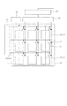
ここで、上述のFPDについて特許文献1を例に図を用いて以下に説明する。ここでは、説明の簡略化のために3×3の2次元マトリクス状に配列されたFPDを例にして説明する。 Here, the FPD described above will be described below with reference to FIG. Here, for simplification of description, an FPD arranged in a 3 × 3 two-dimensional matrix will be described as an example.
図6は、特許文献1に記載された、従来のFPDの等価回路を示す模式的等価回路図である。図7は、特許文献1に記載された、従来のFPDの1画素の模式的平面図である。図8は、図7のX−X’における模式的断面図である。
FIG. 6 is a schematic equivalent circuit diagram showing an equivalent circuit of a conventional FPD described in
入射された放射線に応じて波長変換体より発光された光が、光電変換用のバイアス電圧が印加された複数の光電変換素子各々において信号電荷に変換される。各々の光電変換素子によって変換された信号電荷は、駆動回路によって駆動配線に印加された駆動信号に応じて複数のスイッチング素子が転送動作を行うことにより、信号配線を伝送して信号処理回路に並列的に読み出される。並列的に読み出された信号電荷は信号処理回路によって直列信号に変換され、A/D変換部によってアナログ信号からデジタル信号に変換されて出力される。以上の動作により入射された画像情報を有する放射線に応じた1画像分の画像信号が得られる。 The light emitted from the wavelength converter according to the incident radiation is converted into signal charges in each of the plurality of photoelectric conversion elements to which a bias voltage for photoelectric conversion is applied. The signal charges converted by the respective photoelectric conversion elements are transferred in parallel by the plurality of switching elements in accordance with the drive signal applied to the drive wiring by the drive circuit, so that the signal wiring is transmitted in parallel Read out automatically. The signal charges read in parallel are converted into a serial signal by a signal processing circuit, converted from an analog signal to a digital signal by an A / D converter, and output. Through the above operation, an image signal for one image corresponding to the radiation having image information incident thereon is obtained.
上述のFPDを用いた放射線検出装置において、駆動配線は行方向に配列された複数のスイッチング素子のゲート電極に駆動信号を印加するための駆動回路に接続されている。また、信号配線は列方向に配列された複数のスイッチング素子のソース又はドレイン電極から光電変換素子で発生した信号電荷を処理するための信号処理回路に接続されている。また更に、バイアス配線は光電変換素子が光電変換するための第1の電圧値と、光電変換素子を初期状態にするためのバイアスを印加するための第2の電圧値とを有するバイアス電源部に接続されている。このような各配線と各外部回路との接続は、各配線の一端に設けられた各端子部において電気的に接続されている。ここで、特許文献2に開示されているFPDを用いた放射線検出装置の端子部について説明する。 In the radiation detection apparatus using the FPD described above, the drive wiring is connected to a drive circuit for applying a drive signal to the gate electrodes of a plurality of switching elements arranged in the row direction. The signal wiring is connected to a signal processing circuit for processing signal charges generated by the photoelectric conversion elements from the source or drain electrodes of the plurality of switching elements arranged in the column direction. Furthermore, the bias wiring is connected to a bias power supply unit having a first voltage value for photoelectric conversion by the photoelectric conversion element and a second voltage value for applying a bias for setting the photoelectric conversion element to an initial state. It is connected. Such connection between each wiring and each external circuit is electrically connected at each terminal portion provided at one end of each wiring. Here, the terminal part of the radiation detection apparatus using FPD currently disclosed by patent document 2 is demonstrated.
各端子部は、画素領域の外部の領域すべてにおいて光電変換素子及びスイッチング素子を被覆する保護層を除去して接続領域(開口領域)を形成し、各ICとそれぞれ接続されている。 Each terminal portion is connected to each IC by forming a connection region (opening region) by removing the protective layer covering the photoelectric conversion element and the switching element in the entire region outside the pixel region.
そして、これら各ICが接続された放射線検出装置は、特許文献3に開示されているように、絶縁性基板上の各ICが封止部材(不図示)によって被覆されて、外部から保護されている。
しかしながら、上記FPDを用いた放射線検出装置において、各端子部に腐食が発生する場合がある。これは、各端子部は接続領域において保護層がすべて除去されて剥き出しの状態となっているため、大気中の水分や不純物などに汚染されやすい状態にある。特許文献3に開示されているように各端子部には封止部材が設けられているが、封止部材と絶縁性基板との界面からの水分や不純物を十分に遮断することはできない。そのため、各端子部の側面及び絶縁性基板との界面からの水分や不純物による汚染を十分抑制することができない。特に、医療検査用に用いられる放射線検出装置においては、消毒用のアルコールや水分などが直接放射線検出装置にかかる可能性があり、そのための対策が求められる。 However, in the radiation detection apparatus using the FPD, corrosion may occur in each terminal portion. This is because each terminal portion is exposed by removing all of the protective layer in the connection region, and thus is easily contaminated by moisture, impurities, and the like in the atmosphere. As disclosed in Patent Document 3, each terminal portion is provided with a sealing member. However, moisture and impurities from the interface between the sealing member and the insulating substrate cannot be sufficiently blocked. For this reason, it is impossible to sufficiently suppress contamination due to moisture and impurities from the side surfaces of the terminal portions and the interface with the insulating substrate. In particular, in radiation detection apparatuses used for medical examinations, alcohol for sterilization, moisture, or the like may be directly applied to the radiation detection apparatus, and measures for that are required.
また、各端子部は接続領域において保護層がすべて除去されて剥き出しの状態となっているため、隣接する各端子部の間に導電性接着剤が入り込んでしまった場合には、隣接する各端子部の間でショートが発生する可能性がある。そのため所望の駆動動作や画像の取得を行うことができなくなり、信頼性及び製造工程における歩留まりが低下する可能性がある。 In addition, since each terminal portion is exposed by removing all the protective layer in the connection region, if a conductive adhesive enters between adjacent terminal portions, each adjacent terminal There is a possibility that a short circuit occurs between the parts. Therefore, it becomes impossible to perform a desired driving operation and image acquisition, and there is a possibility that the reliability and the yield in the manufacturing process are lowered.
本発明に係る変換装置及び放射線検出装置は、絶縁性の基板上に設けられたスイッチング素子と、該スイッチング素子よりも上に設けられた半導体層を有して前記スイッチング素子に接続された変換素子と、を含む画素と、外部回路に接続するための端子と、前記端子と前記画素とを接続するための配線と、を有し、前記配線が、前記変換素子にバイアスを印加するためのバイアス配線を含み、前記バイアス配線が、前記半導体層よりも上に設けられた金属層を含む、変換装置であって、前記端子は、前記金属層と同じ層の形成工程で形成された同一の金属層が前記基板上に設けられた端子部と、前記端子部の表面及び側面を被覆して前記基板と接する合金酸化材料の導電層と、を含み、前記端子部の表面の上に位置する前記導電層の表面の少なくとも一部の上に開口を有する保護層によって、前記導電層の前記基板側の界面の端部が被覆されていることを特徴とするものである。 A conversion device and a radiation detection device according to the present invention include a switching element provided on an insulating substrate, and a conversion element connected to the switching element, having a semiconductor layer provided above the switching element. And a terminal for connecting to an external circuit, and a wiring for connecting the terminal and the pixel, the wiring for applying a bias to the conversion element A conversion device including a wiring, wherein the bias wiring includes a metal layer provided above the semiconductor layer, wherein the terminal is the same metal formed in the same layer forming step as the metal layer wherein a terminal portion of the layer is provided on the substrate, a conductive layer of an alloy oxide material contact with the substrate to cover the upper and side surfaces of the terminal portion, and located on a surface of the terminal portion Of the surface of the conductive layer The protective layer having an opening over the least part, an end portion of the interface of the substrate side of the conductive layer is characterized in that it is coated.
本発明により、各端子部の側面及び各端子と絶縁性基板との界面からの水分や不純物による汚染を十分抑制することが可能となる。更に、隣接する各端子部の間の絶縁性が高く確保され、信頼性及び製造工程における歩留まりの低下を抑制することが可能となる。 According to the present invention, it is possible to sufficiently suppress contamination due to moisture and impurities from the side surface of each terminal portion and the interface between each terminal and the insulating substrate. Furthermore, high insulation between each adjacent terminal portion is ensured, and it is possible to suppress a decrease in reliability and yield in the manufacturing process.
以下に、本発明を実施するための最良の形態を、図面を用いて詳細に説明する。 The best mode for carrying out the present invention will be described below in detail with reference to the drawings.
(第1の実施形態)
図1〜3を用いて、本発明の第1の実施形態を詳細に説明する。図1は、本発明の第1の実施形態における光電変換装置及び放射線検出装置を説明する概念的平面図である。図2は、本発明の第1の実施形態における光電変換装置及び放射線検出装置の周辺領域を拡大した概念的平面図である。図3は、図2のA−A’における模式的断面図である。また、図1〜3において、図6〜8で示した従来のFPDと同様の構成要素は同一の番号で示し、その詳細な説明は割愛する。
(First embodiment)
The first embodiment of the present invention will be described in detail with reference to FIGS. FIG. 1 is a conceptual plan view for explaining a photoelectric conversion device and a radiation detection device according to the first embodiment of the present invention. FIG. 2 is a conceptual plan view enlarging the peripheral region of the photoelectric conversion device and the radiation detection device according to the first embodiment of the present invention. FIG. 3 is a schematic cross-sectional view taken along line AA ′ of FIG. 1 to 3, the same components as those of the conventional FPD shown in FIGS. 6 to 8 are denoted by the same reference numerals, and detailed description thereof is omitted.
図1〜3において、100は絶縁性基板、101は変換素子である光電変換素子、102はスイッチング素子、103は駆動配線、104は信号配線、105はバイアス配線である。絶縁性基板100は、ガラス基板、石英基板、プラスチック基板などが好適に用いられる。光電変換素子101はa−SiからなるMIS型フォトセンサであり、スイッチング素子はa−SiからなるTFTであり、この光電変換素子101とスイッチング素子102により1つの画素が構成されている。これらの画素が2次元マトリクス状に配置され、画素領域Pを構成している。画素領域Pより外側のコンタクトホール領域Cには、コンタクトホールが配置されている。コンタクトホール領域Cは、画素領域Pから端子部に向かって、絶縁基板からのトータル膜厚が減少するように層が配置されていることが好ましい。このような構成により、段差が小さくなり、段差上に配置される配線の不良が減少する。駆動配線103は行方向に配列された複数のスイッチング素子102のゲート電極110に接続されており、スイッチング素子102のゲート電極110と同一の層である第1の金属層M1によって形成された配線である。信号配線104は列方向に配列された複数のスイッチング素子102のソース又はドレイン電極114に接続されており、スイッチング素子のソース又はドレイン電極114と同一の層である第2の金属層M2によって形成された配線である。バイアス配線105は光電変換素子101にバイアス電圧を印加するために上部電極層120に接続されてセンサ上部電極を構成しており、Alなどの金属材料により形成された第4の金属層M4によって形成された配線である。
1-3, 100 is an insulating substrate, 101 is a photoelectric conversion element which is a conversion element, 102 is a switching element, 103 is a drive wiring, 104 is a signal wiring, and 105 is a bias wiring. As the insulating
本発明の第1の実施形態において、103aは駆動配線引き出し配線部であり、画素領域Pの外側でコンタクトホール126を介して各駆動配線103と接続されている。また、駆動配線引き出し配線部103aには、駆動回路107と電気的に接続するための駆動配線端子部123が設けられている。これら駆動配線引き出し配線部103a及び駆動配線端子部123は、積層構造のFPDにおいて最も上層の金属層であるバイアス配線105と同一の層である第4の金属層M4によって形成されている。そのため、駆動配線引き出し配線部103a上には保護層121が積層されるだけの構造となるため、駆動回路107との電気的接続のために設けられる接続領域(開口領域)OP1の形成が容易である。また、駆動配線引き出し配線部103a及び駆動配線端子部123がバイアス配線105と同じ第4の金属層M4で形成されているため、バイアス配線105と同様に、その表面が上部電極層120により被覆される。そのため、駆動配線端子部123において第4の金属層M4の腐食を低減することが可能となる。
In the first embodiment of the present invention, reference numeral 103 a denotes a drive wiring lead-out wiring portion, which is connected to each
また、104aは信号配線引き出し配線部であり、画素領域Pの外側でコンタクトホール127を介して各信号配線104と接続されている。また、信号配線引き出し配線部104aには、信号処理回路106と電気的に接続するための信号配線端子部124が設けられている。これら信号配線引き出し配線部104a及び信号配線端子部124は、積層構造のFPDにおいて最も上層の金属層であるバイアス配線105と同一の層である第4の金属層M4によって形成されている。そのため、信号配線端子部124の上には保護層121が積層されるだけの構造となるため、信号処理回路106との電気的接続のために設けられる接続領域(開口領域)OP2の形成が容易である。また、信号配線引き出し配線部104a及び信号配線端子部124がバイアス配線105と同じ第4の金属層M4で形成されているため、バイアス配線105と同様に、その表面が上部電極層120により被覆される。そのため、信号配線端子部124において第4の金属層M4の腐食を低減することが可能となる。
Reference numeral 104a denotes a signal wiring lead-out wiring portion, which is connected to each
次に、105aは第1のバイアス配線引き出し配線部であり、画素領域Pの外側でコンタクトホール128を介して各バイアス配線105と接続されている。この第1のバイアス配線引き出し配線部105aは積層構造のFPDにおいて最も下層の金属層である駆動配線103と同一の層である第1の金属層M1によって形成されている。また、第1のバイアス配線引き出し配線部105aはコンタクトホール129を介して第2のバイアス配線引き出し配線部105bと接続されている。さらに第2のバイアス配線引き出し配線部105bには、バイアス電源部109と電気的に接続するためのバイアス配線端子部125が設けられている。ここで、これらバイアス配線引き出し配線部105b及びバイアス配線端子部125は、積層構造のFPDにおいて最も上層の金属層であるバイアス配線105と同一の層である第4の金属層M4によって形成されている。そのため、バイアス配線端子部125の上には保護層121が積層されるだけの構造となるため、バイアス電源部109との電気的接続のために設けられる接続領域(開口領域)OP3の形成が容易である。また、バイアス配線引き出し配線部105b及びバイアス配線端子部125がバイアス配線105と同じ第4の金属層M4で形成されているため、バイアス配線105と同様に、その表面が上部電極層120により被覆される。そのため、バイアス配線端子部125において第4の金属層M4の腐食を防止することが可能となる。
Next,
本実施形態においては、各端子部123〜125はバイアス配線105と同じ第4の金属層M4で、つまり、FPDにおける最も上層の金属層を用いて形成されている。各端子部123〜125として第1の金属層M1や第2の金属層M2を用いてもよいが、最も上層である第4の金属層M4を用いることが好ましい。駆動配線103などを形成している第1の金属層M1は、形成された後に、第1の絶縁層111、第1の半導体層112、第1の不純物半導体層113、第2の金属層M2が積層して形成される。さらに層間絶縁層115が積層され形成される。さらに第3の金属層M3、第2の絶縁層117、第2の半導体層118、第2の不純物半導体層119、第4の金属層M4、上部電極層120、保護層121が積層して形成される。そのため第1の金属層M1はその各層の形成工程において、それぞれ加熱、エッチングなどの処理により層にダメージを受けてしまう。また、信号配線104などを形成している第2の金属層M2も、形成された後に、層間絶縁層115が積層して形成される。さらに第3の金属層M3、第2の絶縁層117、第2の半導体層118、第2の不純物半導体層119、第4の金属層M4、上部電極層120、保護層121が積層して形成される。そのため第2の金属層M2はその各層の形成工程において、それぞれ加熱、エッチングなどの処理により層にダメージを受けてしまう。このような金属層が受けるダメージが大きければ大きいほど、外気の水分や不純物による汚染およびそれによる腐食が起こりやすくなる。例えば、加熱により金属表面が酸化されると、表面の濡れ性が向上し、乾燥が困難となる。その結果、薬液などの洗浄不良がおこり、腐食に繋がることになる。さらに、加熱によって金属層の表面が酸化して電気抵抗が高くなってしまうという問題がある。また、エッチングによる金属層の表面の損傷や、エッチング材料の残渣等による影響により、腐食に繋がることになる。一方、本実施形態のように、各端子部123〜125などを形成する第4の金属層M4は、その上方には保護層121しか形成されない。そのため、第4の金属層M4にダメージを与える工程は保護層121の形成工程と、各端子部123〜125に接続領域(開口領域)OP1〜OP3を設けるための工程だけであるため、他の金属層M1〜M3に比べて受けるダメージは少ない。そのため、第4の金属層M4の表面状態は良好で、外気の水分や不純物による汚染およびそれによる腐食が起こりにくくなる。
In the present embodiment, each of the
次に、図3を用いて、信号配線端子部124とバイアス配線端子部125を例として端子部の断面構造を説明する。図3において、絶縁性基板100上に設けられた信号配線端子部124の表面及び側面を被覆するように、ITOなどの合金酸化材料により形成された透明導電層からなる上部電極層120を設けて、信号配線用端子131を形成している。そして、少なくとも信号配線用端子131の絶縁性基板100との接触界面(信号配線用端子131の端部)を被覆するように保護層121及び接続領域(開口領域)OP2を設ける。同様に、絶縁性基板100上に設けられたバイアス配線端子部125の表面及び側面を被覆するように、上部電極層120を設けて、バイアス配線用端子132を形成している。そして、少なくともバイアス配線用端子132の絶縁性基板100との接触界面(バイアス配線用端子132の端部)を被覆するように保護層121及び接続領域(開口領域)OP3を設ける。ここで、図示していないが、駆動配線端子部123も同様にその表面及び側面が被覆されるように上部電極層120が設けられて駆動配線用端子130(不図示)が構成されている。更に、少なくともこの駆動配線用端子130の絶縁性基板100との接触界面(駆動配線用端子130の端部)を被覆するように保護層121及び接続領域(開口領域)OP1が設けられている。このような構成とすることにより、各端子部123〜125の側面及び各端子130〜132と絶縁性基板100との界面からの水分や不純物による汚染を十分抑制することが可能となる。ここで、本実施形態では各端子部123〜125が上部電極層120によって被覆されている形態を示した。しかしながら、本発明はそれに限定されることはなく、各端子部123〜125の側面及び絶縁性基板100との接触界面を被覆するように保護層121及び各接続領域OP1〜OP3を設けても構わない。しかしながら、金属材料より耐湿性に優れた合金酸化材料からなる透明導電層である上部電極層120によって金属層からなる各端子部123〜125を被覆することによって、より良好に大気中の水分や不純物による汚染を抑制することが可能となる。
Next, the cross-sectional structure of the terminal portion will be described with reference to FIG. 3 using the signal
また本実施形態では、隣接する端子部の間に各端子部の側面及び絶縁性基板100との接触界面を被覆するように保護層121を除去せずに配置している。図3においては、信号配線用端子131とバイアス配線用端子132との間に、各端子131,132の側面及び絶縁性基板100との接触界面を被覆するように保護層121を除去せずに配置している。このように、隣接する各端子部の間に保護層121を配置している。このような構成とすることにより、外部回路を有する各ICと接続するための導電性接着剤が隣接する端子部に流入することにより発生するショートを防ぐことが可能となる。そのため各端子部の間の絶縁性が高く確保され、信頼性及び製造工程における歩留まりの低下を抑制することが可能となる。
Moreover, in this embodiment, it arrange | positions without removing the
また、各端子130〜132の絶縁性基板100との接触界面(各端子130〜132の端部)を被覆するように保護層121が設けられている。しかしながら本発明はこれに限定されるものではなく、保護層121とは別途設けられた、少なくとも各配線もしくは各端子130〜132を被覆する保護層により接触界面(端部)が被覆されていてもよい。
Moreover, the
ここで、本実施形態では、光電変換素子101としてMIS型フォトセンサを用いた積層構造のMIS型FPDについて説明したが、図4に示すような光電変換素子としてPIN型フォトダイオード134を用いたPIN型FPDを用いてもよい。図4において、133は第2の不純物半導体層119と異なる導電型の不純物が導入された第3の不純物半導体層である。PIN型フォトダイオードにおいては第2の不純物半導体層119はn型のa−Si層が、第3の不純物半導体層133はP型のa−Si層が好適に用いられる。また、光電変換素子101上には、放射線を可視光に変換する波長変換体122が配置されている。また、本実施の形態では、スイッチング素子102であるTFTとしてギャップエッチング型のTFTを用いて説明した。しかしながら本発明はそれに限られるものではなく、たとえばギャップストッパー型のTFTや、poly−Si TFTで採用されるプレイナー型のTFTを用いてもよい。即ち、スイッチング素子102と光電変換素子101との組み合わせで、少なくとも駆動配線103、信号配線104、バイアス配線105の3層以上の金属層を使用した場合には、本発明に従って改良可能なものである。また、本実施の形態では、信号配線104やソース又はドレイン電極114を第2の金属層M2で、センサ下部電極を第3の金属層M3でそれぞれ別の金属層を用いて形成している。しかしながら本発明はそれに限られるものではなく、信号配線104やソース又はドレイン電極114とセンサ下部電極(第3の金属層)116とを同一の金属層を用いて形成してもよい。ただし、その場合には信号配線104とセンサ下部電極とを重ねて配置することができず、また、光電変換素子をスイッチング素子上には完全に重ねることができないため、FPDの開口率は異なる金属層を用いて形成されたものに比べると低下してしまう。また本実施形態では、変換素子としてa−Siからなる第2の半導体層118を用いたMIS型フォトセンサ101及びPIN型フォトダイオードを用いたFPDを用いて説明した。しかしながら本発明はこれに限定されるものでなく、変換素子としてa−SeやCdTeを第2の半導体層として用いた、放射線を直接電荷に変換する変換素子を用いたFPDを用いてもよい。
Here, in the present embodiment, the MIS type FPD having a laminated structure using the MIS type photosensor as the
(応用例)
図5は、本発明によるFPD型の放射線検出装置を用いたX線診断システムへの応用例を示したものである。
(Application examples)
FIG. 5 shows an application example to an X-ray diagnosis system using the FPD type radiation detection apparatus according to the present invention.
X線チューブ6050で発生したX線6060は患者あるいは被験者6061の胸部6062を透過し、シンチレータ(蛍光体)を上部に実装した放射線検出装置6040に入射する。この入射したX線には患者6061の体内部の情報が含まれている。X線の入射に対応してシンチレータは発光し、これを光電変換して、電気的情報を得る。この情報はディジタルに変換され信号処理手段となるイメージプロセッサ6070により画像処理され制御室の表示手段となるディスプレイ6080で観察できる。
The
また、イメージプロセッサ6070は、イメージセンサ6040から出力された電気信号を電話回線6090等の伝送処理手段を介して遠隔地へ転送し、ドクタールーム等の別の場所にある表示手段(ディスプレイ)6081に表示することもできる。また、イメージセンサ6040から出力された電気信号を光ディスク等の記録手段に保存し、この記録手段を用いて遠隔地の医師が診断することも可能である。また、記録手段となるフィルムプロセッサ6100によりフィルム6110に記録することもできる。
Further, the
本発明は、医療診断機器、非破壊検査機器等に用いられる、光電変換装置、放射線検出用基板及び放射線検出装置に用いられるものである。 The present invention is used for a photoelectric conversion device, a radiation detection substrate, and a radiation detection device that are used in medical diagnostic equipment, non-destructive testing equipment, and the like.
100 絶縁性基板
101 光電変換素子(MIS型フォトセンサ)
102 スイッチング素子
103 駆動配線
103a 駆動配線引き出し部
104 信号配線
104a 信号配線引き出し部
105 バイアス配線
105a 第1のバイアス配線引き出し部
105b 第2のバイアス配線引き出し部
106 信号処理回路
107 駆動回路
108 A/D変換部
109 バイアス電源部
110 第1の金属層M1(スイッチング素子102のゲート電極)
111 第1の絶縁層
112 第1の半導体層
113 第1の不純物半導体層
114 第2の金属層M2(スイッチング素子102のソース又はドレイン電極)
115 層間絶縁層
116 第3の金属層M3(センサ下部電極)
117 第2の絶縁層
118 第2の半導体層
119 第2の不純物半導体層
120 上部電極層(透明電極層)
121 保護層
122 波長変換体
123 駆動配線端子部
124 信号配線端子部
125 バイアス配線端子部
126〜129 コンタクト
131 信号配線用端子
132 バイアス配線用端子
133 第3の不純物半導体層
134 光電変換素子(PIN型フォトダイオード)
100 Insulating
DESCRIPTION OF
111 first insulating
115
117
121
Claims (7)
外部回路と接続するための端子と、
前記端子と前記画素とを接続するための配線と、
を有し、
前記配線が、前記変換素子にバイアスを印加するためのバイアス配線を含み、
前記バイアス配線が、前記半導体層よりも上に設けられた金属層を含む、変換装置であって、
前記端子は、前記金属層と同じ層の形成工程で形成された同一の金属層が前記基板上に設けられた端子部と、前記端子部の表面及び側面を被覆して前記基板と接する合金酸化材料の導電層と、を含み、前記端子部の表面の上に位置する前記導電層の表面の少なくとも一部の上に開口を有する保護層によって、前記導電層の前記基板側の界面の端部が被覆されていることを特徴とする変換装置。 A pixel including a switching element provided on an insulating substrate, and a conversion element having a semiconductor layer provided above the switching element and connected to the switching element;
A terminal for connecting to an external circuit;
A wiring for connecting the terminal and the pixel;
Have
The wiring includes a bias wiring for applying a bias to the conversion element;
The bias wiring includes a metal layer provided above the semiconductor layer, the conversion device comprising:
The terminal includes: the metal layer and the terminal portion of the same metal layer formed by forming process is provided on the substrate in the same layer, an alloy into contact with the substrate to cover the upper and side surfaces of the terminal portion A conductive layer of an oxide material, and an end of an interface on the substrate side of the conductive layer by a protective layer having an opening on at least a part of the surface of the conductive layer located on the surface of the terminal portion A conversion device characterized in that the part is covered.
前記変換素子は、前記スイッチング素子よりも上に設けられ前記ソース電極及び前記ドレイン電極の一方に接続された第1電極と、前記第1電極よりも上に設けられた前記半導体層と、前記半導体層よりも上に設けられた第2電極と、を含み、
前記配線は、前記ゲート電極に接続された駆動配線、前記ソース電極及び前記ドレイン電極の他方に接続された信号配線、のうちのいずれか一つを更に含むことを特徴とする請求項1に記載の変換装置。 The switching element is a transistor including a gate electrode, a source electrode, and a drain electrode,
The conversion element includes a first electrode provided above the switching element and connected to one of the source electrode and the drain electrode, the semiconductor layer provided above the first electrode, and the semiconductor A second electrode provided above the layer,
The wiring according to claim 1, wherein the further comprising the connected drive wiring to the gate electrode, and the other is to connect the signal line of the source electrode and the drain electrode, any one of Conversion device.
前記バイアス配線は、前記透明導電層により被覆されていることを特徴とする請求項2に記載の変換装置。 The second electrode is a transparent conductive layer of an alloy oxide material formed simultaneously with the conductive layer,
The conversion device according to claim 2, wherein the bias wiring is covered with the transparent conductive layer.
前記変換装置の前記変換素子上に配された、入射した放射線を可視光に変換するための波長変換体を更に有することを特徴とする放射線検出装置。 The conversion device according to any one of claims 1 to 5 ,
The radiation detection apparatus further comprising a wavelength converter disposed on the conversion element of the conversion apparatus for converting incident radiation into visible light.
前記放射線検出装置からの信号を処理する信号処理手段と、
前記信号処理手段からの信号を記録するための記録手段と、
前記信号処理手段からの信号を表示するための表示手段と、
前記信号処理手段からの信号を伝送するための伝送処理手段と、
前記放射線を発生させるための放射線源と、
を具備することを特徴とする放射線検出システム。 A radiation detection apparatus according to claim 6 ;
Signal processing means for processing signals from the radiation detection device;
Recording means for recording a signal from the signal processing means;
Display means for displaying a signal from the signal processing means;
Transmission processing means for transmitting a signal from the signal processing means;
A radiation source for generating the radiation;
A radiation detection system comprising:
Priority Applications (3)
| Application Number | Priority Date | Filing Date | Title |
|---|---|---|---|
| JP2006181890A JP4908947B2 (en) | 2005-07-11 | 2006-06-30 | Conversion device, radiation detection device, and radiation detection system |
| US11/456,155 US7429723B2 (en) | 2005-07-11 | 2006-07-07 | Conversion apparatus, radiation detection apparatus, and radiation detection system |
| US12/184,522 US7655920B2 (en) | 2005-07-11 | 2008-08-01 | Conversion apparatus, radiation detection apparatus, and radiation detection system |
Applications Claiming Priority (3)
| Application Number | Priority Date | Filing Date | Title |
|---|---|---|---|
| JP2005201603 | 2005-07-11 | ||
| JP2005201603 | 2005-07-11 | ||
| JP2006181890A JP4908947B2 (en) | 2005-07-11 | 2006-06-30 | Conversion device, radiation detection device, and radiation detection system |
Publications (3)
| Publication Number | Publication Date |
|---|---|
| JP2007049122A JP2007049122A (en) | 2007-02-22 |
| JP2007049122A5 JP2007049122A5 (en) | 2011-10-20 |
| JP4908947B2 true JP4908947B2 (en) | 2012-04-04 |
Family
ID=37617470
Family Applications (1)
| Application Number | Title | Priority Date | Filing Date |
|---|---|---|---|
| JP2006181890A Expired - Fee Related JP4908947B2 (en) | 2005-07-11 | 2006-06-30 | Conversion device, radiation detection device, and radiation detection system |
Country Status (2)
| Country | Link |
|---|---|
| US (2) | US7429723B2 (en) |
| JP (1) | JP4908947B2 (en) |
Families Citing this family (18)
| Publication number | Priority date | Publication date | Assignee | Title |
|---|---|---|---|---|
| JP4908947B2 (en) * | 2005-07-11 | 2012-04-04 | キヤノン株式会社 | Conversion device, radiation detection device, and radiation detection system |
| KR101350795B1 (en) * | 2007-06-11 | 2014-01-10 | 삼성디스플레이 주식회사 | Thin film transistor array substrate for x-ray detector |
| JP5235350B2 (en) * | 2007-08-07 | 2013-07-10 | キヤノン株式会社 | Imaging apparatus and radiation imaging system |
| JP2009252835A (en) | 2008-04-02 | 2009-10-29 | Fujifilm Corp | Electromagnetic wave detecting element |
| KR101469042B1 (en) * | 2008-08-29 | 2014-12-05 | 삼성디스플레이 주식회사 | X-ray detecting panel and x-ray detector |
| JP5439984B2 (en) * | 2009-07-03 | 2014-03-12 | ソニー株式会社 | Photoelectric conversion device and radiation imaging device |
| TWI424574B (en) * | 2009-07-28 | 2014-01-21 | Prime View Int Co Ltd | Digital x ray detecting panel and method for manufacturing the same |
| JP2011159781A (en) * | 2010-02-01 | 2011-08-18 | Epson Imaging Devices Corp | Photoelectric conversion device, x-ray imaging device, and method of manufacturing photoelectric conversion device |
| JP2011159782A (en) * | 2010-02-01 | 2011-08-18 | Epson Imaging Devices Corp | Photoelectric conversion device, x-ray imaging device, and method of manufacturing photoelectric conversion device |
| JP2011238897A (en) * | 2010-04-13 | 2011-11-24 | Canon Inc | Detection device, manufacturing method thereof, and detection system |
| JP5700973B2 (en) | 2010-08-05 | 2015-04-15 | キヤノン株式会社 | Detection apparatus and radiation detection system |
| JP2015092518A (en) * | 2012-02-22 | 2015-05-14 | 富士フイルム株式会社 | Semiconductor element, radiation detector, and manufacturing method of the semiconductor element |
| CN102790069B (en) * | 2012-07-26 | 2014-09-10 | 北京京东方光电科技有限公司 | Sensor and manufacturing method thereof |
| JP5709810B2 (en) * | 2012-10-02 | 2015-04-30 | キヤノン株式会社 | Detection device manufacturing method, detection device and detection system |
| US10276611B2 (en) * | 2015-06-04 | 2019-04-30 | Sharp Kabushiki Kaisha | Photosensor substrate |
| CN108318907B (en) * | 2018-02-01 | 2019-10-01 | 北京京东方光电科技有限公司 | X-ray detection panel and its manufacturing method and X-ray detection device |
| JP2019145595A (en) * | 2018-02-16 | 2019-08-29 | シャープ株式会社 | Active matrix substrate, X-ray imaging panel including the same, and manufacturing method |
| CN109490933B (en) * | 2018-10-22 | 2020-05-01 | 京东方科技集团股份有限公司 | Flat panel detector, detection method thereof and X-ray detection device |
Family Cites Families (17)
| Publication number | Priority date | Publication date | Assignee | Title |
|---|---|---|---|---|
| JPH06160877A (en) | 1992-11-25 | 1994-06-07 | Hitachi Ltd | Thin-film wiring structure and liquid crystal display device formed by using the structure |
| JPH07183324A (en) | 1993-12-22 | 1995-07-21 | Sony Corp | Semiconductor device |
| FR2758630B1 (en) * | 1997-01-21 | 1999-04-09 | Thomson Tubes Electroniques | PROCESS FOR SEALING A SOLID STATE RADIATION DETECTOR AND DETECTOR OBTAINED THEREBY |
| JP2001251557A (en) * | 1999-12-27 | 2001-09-14 | Canon Inc | Area sensor, image input device having the same and method for driving the area sensor |
| US6765187B2 (en) * | 2001-06-27 | 2004-07-20 | Canon Kabushiki Kaisha | Imaging apparatus |
| JP2003319270A (en) | 2002-04-24 | 2003-11-07 | Canon Inc | Image pickup apparatus composed of light or radiation sensor and inspecting method therefor |
| JP2003347534A (en) * | 2002-05-28 | 2003-12-05 | Canon Inc | Radiation detection apparatus and its manufacturing method |
| JP4054612B2 (en) | 2002-06-11 | 2008-02-27 | キヤノン株式会社 | Radiation imaging device |
| JP4018461B2 (en) * | 2002-06-11 | 2007-12-05 | キヤノン株式会社 | Radiation detection apparatus, method of manufacturing the same, and radiation imaging system |
| US7214945B2 (en) * | 2002-06-11 | 2007-05-08 | Canon Kabushiki Kaisha | Radiation detecting apparatus, manufacturing method therefor, and radiation image pickup system |
| US7148487B2 (en) * | 2002-08-27 | 2006-12-12 | Canon Kabushiki Kaisha | Image sensing apparatus and method using radiation |
| JP4502575B2 (en) * | 2002-11-06 | 2010-07-14 | 奇美電子股▲ふん▼有限公司 | Wiring formation method for display device |
| EP1420453B1 (en) * | 2002-11-13 | 2011-03-09 | Canon Kabushiki Kaisha | Image pickup apparatus, radiation image pickup apparatus and radiation image pickup system |
| JP2004281998A (en) * | 2003-01-23 | 2004-10-07 | Seiko Epson Corp | Transistor, its manufacturing method, electro-optical device, semiconductor device and electronic apparatus |
| JP4266656B2 (en) * | 2003-02-14 | 2009-05-20 | キヤノン株式会社 | Solid-state imaging device and radiation imaging device |
| JP2004296654A (en) * | 2003-03-26 | 2004-10-21 | Canon Inc | Radiation imaging device |
| JP4908947B2 (en) * | 2005-07-11 | 2012-04-04 | キヤノン株式会社 | Conversion device, radiation detection device, and radiation detection system |
-
2006
- 2006-06-30 JP JP2006181890A patent/JP4908947B2/en not_active Expired - Fee Related
- 2006-07-07 US US11/456,155 patent/US7429723B2/en active Active
-
2008
- 2008-08-01 US US12/184,522 patent/US7655920B2/en not_active Expired - Fee Related
Also Published As
| Publication number | Publication date |
|---|---|
| US7429723B2 (en) | 2008-09-30 |
| JP2007049122A (en) | 2007-02-22 |
| US20080290284A1 (en) | 2008-11-27 |
| US7655920B2 (en) | 2010-02-02 |
| US20070007458A1 (en) | 2007-01-11 |
Similar Documents
| Publication | Publication Date | Title |
|---|---|---|
| JP4908947B2 (en) | Conversion device, radiation detection device, and radiation detection system | |
| JP5043374B2 (en) | Conversion device, radiation detection device, and radiation detection system | |
| JP5043373B2 (en) | Conversion device, radiation detection device, and radiation detection system | |
| JP4845352B2 (en) | Radiation imaging apparatus, manufacturing method thereof, and radiation imaging system | |
| US8067743B2 (en) | Imaging apparatus and radiation imaging apparatus | |
| EP2168370B1 (en) | Radiation detecting apparatus and radiation imaging system | |
| JP5235350B2 (en) | Imaging apparatus and radiation imaging system | |
| JP5196739B2 (en) | Radiation imaging apparatus and radiation imaging system | |
| JP5142943B2 (en) | Radiation detection device manufacturing method, radiation detection device and radiation imaging system | |
| JP4498283B2 (en) | Imaging apparatus, radiation imaging apparatus, and manufacturing method thereof | |
| JP2012079820A (en) | Detector and radiation detection system | |
| JP2004015000A (en) | Radiation detector and radiation imaging systems | |
| JP2005116543A (en) | Imaging device, its manufacturing method, radiation imaging device, and radiation imaging system | |
| JP2006128644A (en) | Imaging apparatus, radiation imaging apparatus, and radiation imaging system | |
| JP4018461B2 (en) | Radiation detection apparatus, method of manufacturing the same, and radiation imaging system | |
| JP5789223B2 (en) | Radiation imaging apparatus and radiation imaging system | |
| JP2005003444A (en) | Radiation detector and radiation imaging system | |
| JP2006128645A (en) | Imaging apparatus, radiation imaging apparatus, and radiation imaging system | |
| JP2018195949A (en) | Radiation imaging device and radiation imaging system | |
| JP2007281690A (en) | Electromagnetic wave detector and radiation imaging system | |
| JP2005129715A (en) | Radiation detector | |
| JP2007103577A (en) | Electromagnetic wave detector and radiation imaging system |
Legal Events
| Date | Code | Title | Description |
|---|---|---|---|
| A521 | Request for written amendment filed |
Free format text: JAPANESE INTERMEDIATE CODE: A523 Effective date: 20090604 |
|
| A621 | Written request for application examination |
Free format text: JAPANESE INTERMEDIATE CODE: A621 Effective date: 20090604 |
|
| RD04 | Notification of resignation of power of attorney |
Free format text: JAPANESE INTERMEDIATE CODE: A7424 Effective date: 20100201 |
|
| RD01 | Notification of change of attorney |
Free format text: JAPANESE INTERMEDIATE CODE: A7421 Effective date: 20100630 |
|
| A521 | Request for written amendment filed |
Free format text: JAPANESE INTERMEDIATE CODE: A523 Effective date: 20110905 |
|
| A871 | Explanation of circumstances concerning accelerated examination |
Free format text: JAPANESE INTERMEDIATE CODE: A871 Effective date: 20110905 |
|
| A975 | Report on accelerated examination |
Free format text: JAPANESE INTERMEDIATE CODE: A971005 Effective date: 20110916 |
|
| A131 | Notification of reasons for refusal |
Free format text: JAPANESE INTERMEDIATE CODE: A131 Effective date: 20111004 |
|
| A521 | Request for written amendment filed |
Free format text: JAPANESE INTERMEDIATE CODE: A523 Effective date: 20111205 |
|
| TRDD | Decision of grant or rejection written | ||
| A01 | Written decision to grant a patent or to grant a registration (utility model) |
Free format text: JAPANESE INTERMEDIATE CODE: A01 Effective date: 20120110 |
|
| A01 | Written decision to grant a patent or to grant a registration (utility model) |
Free format text: JAPANESE INTERMEDIATE CODE: A01 |
|
| A61 | First payment of annual fees (during grant procedure) |
Free format text: JAPANESE INTERMEDIATE CODE: A61 Effective date: 20120113 |
|
| FPAY | Renewal fee payment (event date is renewal date of database) |
Free format text: PAYMENT UNTIL: 20150120 Year of fee payment: 3 |
|
| R151 | Written notification of patent or utility model registration |
Ref document number: 4908947 Country of ref document: JP Free format text: JAPANESE INTERMEDIATE CODE: R151 |
|
| FPAY | Renewal fee payment (event date is renewal date of database) |
Free format text: PAYMENT UNTIL: 20150120 Year of fee payment: 3 |
|
| LAPS | Cancellation because of no payment of annual fees |