JP5514474B2 - 薄膜トランジスタの作製方法、不揮発性半導体記憶素子の作製方法 - Google Patents
薄膜トランジスタの作製方法、不揮発性半導体記憶素子の作製方法 Download PDFInfo
- Publication number
- JP5514474B2 JP5514474B2 JP2009130819A JP2009130819A JP5514474B2 JP 5514474 B2 JP5514474 B2 JP 5514474B2 JP 2009130819 A JP2009130819 A JP 2009130819A JP 2009130819 A JP2009130819 A JP 2009130819A JP 5514474 B2 JP5514474 B2 JP 5514474B2
- Authority
- JP
- Japan
- Prior art keywords
- resist mask
- film
- layer
- semiconductor
- conductive
- Prior art date
- Legal status (The legal status is an assumption and is not a legal conclusion. Google has not performed a legal analysis and makes no representation as to the accuracy of the status listed.)
- Expired - Fee Related
Links
- 239000004065 semiconductor Substances 0.000 title claims description 317
- 238000000034 method Methods 0.000 title claims description 150
- 239000010409 thin film Substances 0.000 title claims description 93
- 238000004519 manufacturing process Methods 0.000 title claims description 72
- 239000010408 film Substances 0.000 claims description 517
- 239000012535 impurity Substances 0.000 claims description 125
- 238000005530 etching Methods 0.000 claims description 67
- QVGXLLKOCUKJST-UHFFFAOYSA-N atomic oxygen Chemical compound [O] QVGXLLKOCUKJST-UHFFFAOYSA-N 0.000 claims description 29
- 239000001301 oxygen Substances 0.000 claims description 29
- 229910052760 oxygen Inorganic materials 0.000 claims description 29
- 238000004380 ashing Methods 0.000 claims description 26
- XLYOFNOQVPJJNP-UHFFFAOYSA-N water Substances O XLYOFNOQVPJJNP-UHFFFAOYSA-N 0.000 claims description 21
- CBENFWSGALASAD-UHFFFAOYSA-N Ozone Chemical compound [O-][O+]=O CBENFWSGALASAD-UHFFFAOYSA-N 0.000 claims description 14
- 238000009832 plasma treatment Methods 0.000 claims description 3
- 239000010410 layer Substances 0.000 description 320
- 239000000758 substrate Substances 0.000 description 50
- 239000000463 material Substances 0.000 description 48
- 238000001312 dry etching Methods 0.000 description 41
- 238000000206 photolithography Methods 0.000 description 40
- 238000005229 chemical vapour deposition Methods 0.000 description 32
- 238000004544 sputter deposition Methods 0.000 description 32
- 230000007261 regionalization Effects 0.000 description 31
- 239000007789 gas Substances 0.000 description 26
- 238000001039 wet etching Methods 0.000 description 19
- 239000013078 crystal Substances 0.000 description 18
- 239000011241 protective layer Substances 0.000 description 18
- 239000004020 conductor Substances 0.000 description 13
- 239000011810 insulating material Substances 0.000 description 10
- VYZAMTAEIAYCRO-UHFFFAOYSA-N Chromium Chemical compound [Cr] VYZAMTAEIAYCRO-UHFFFAOYSA-N 0.000 description 6
- 239000001257 hydrogen Substances 0.000 description 6
- 229910052739 hydrogen Inorganic materials 0.000 description 6
- 239000011159 matrix material Substances 0.000 description 6
- UFHFLCQGNIYNRP-UHFFFAOYSA-N Hydrogen Chemical compound [H][H] UFHFLCQGNIYNRP-UHFFFAOYSA-N 0.000 description 5
- 239000003990 capacitor Substances 0.000 description 5
- 239000011651 chromium Substances 0.000 description 5
- 229910052804 chromium Inorganic materials 0.000 description 5
- 238000000151 deposition Methods 0.000 description 5
- 230000008021 deposition Effects 0.000 description 5
- KRHYYFGTRYWZRS-UHFFFAOYSA-N Fluorane Chemical compound F KRHYYFGTRYWZRS-UHFFFAOYSA-N 0.000 description 4
- XUIMIQQOPSSXEZ-UHFFFAOYSA-N Silicon Chemical compound [Si] XUIMIQQOPSSXEZ-UHFFFAOYSA-N 0.000 description 4
- 230000015572 biosynthetic process Effects 0.000 description 4
- 229910052710 silicon Inorganic materials 0.000 description 4
- 239000010703 silicon Substances 0.000 description 4
- 239000011521 glass Substances 0.000 description 3
- IJGRMHOSHXDMSA-UHFFFAOYSA-N Atomic nitrogen Chemical compound N#N IJGRMHOSHXDMSA-UHFFFAOYSA-N 0.000 description 2
- ZOXJGFHDIHLPTG-UHFFFAOYSA-N Boron Chemical compound [B] ZOXJGFHDIHLPTG-UHFFFAOYSA-N 0.000 description 2
- VEXZGXHMUGYJMC-UHFFFAOYSA-N Hydrochloric acid Chemical compound Cl VEXZGXHMUGYJMC-UHFFFAOYSA-N 0.000 description 2
- OAICVXFJPJFONN-UHFFFAOYSA-N Phosphorus Chemical compound [P] OAICVXFJPJFONN-UHFFFAOYSA-N 0.000 description 2
- BLRPTPMANUNPDV-UHFFFAOYSA-N Silane Chemical compound [SiH4] BLRPTPMANUNPDV-UHFFFAOYSA-N 0.000 description 2
- VYPSYNLAJGMNEJ-UHFFFAOYSA-N Silicium dioxide Chemical compound O=[Si]=O VYPSYNLAJGMNEJ-UHFFFAOYSA-N 0.000 description 2
- QAOWNCQODCNURD-UHFFFAOYSA-N Sulfuric acid Chemical compound OS(O)(=O)=O QAOWNCQODCNURD-UHFFFAOYSA-N 0.000 description 2
- 229910052796 boron Inorganic materials 0.000 description 2
- 239000006229 carbon black Substances 0.000 description 2
- 238000006243 chemical reaction Methods 0.000 description 2
- 230000000694 effects Effects 0.000 description 2
- 230000005669 field effect Effects 0.000 description 2
- 238000005468 ion implantation Methods 0.000 description 2
- 229910052698 phosphorus Inorganic materials 0.000 description 2
- 239000011574 phosphorus Substances 0.000 description 2
- 238000005268 plasma chemical vapour deposition Methods 0.000 description 2
- 238000011946 reduction process Methods 0.000 description 2
- 239000011347 resin Substances 0.000 description 2
- 229920005989 resin Polymers 0.000 description 2
- 229910052814 silicon oxide Inorganic materials 0.000 description 2
- ZAMOUSCENKQFHK-UHFFFAOYSA-N Chlorine atom Chemical compound [Cl] ZAMOUSCENKQFHK-UHFFFAOYSA-N 0.000 description 1
- PXGOKWXKJXAPGV-UHFFFAOYSA-N Fluorine Chemical compound FF PXGOKWXKJXAPGV-UHFFFAOYSA-N 0.000 description 1
- 241000255777 Lepidoptera Species 0.000 description 1
- WGLPBDUCMAPZCE-UHFFFAOYSA-N Trioxochromium Chemical compound O=[Cr](=O)=O WGLPBDUCMAPZCE-UHFFFAOYSA-N 0.000 description 1
- QZPSXPBJTPJTSZ-UHFFFAOYSA-N aqua regia Chemical compound Cl.O[N+]([O-])=O QZPSXPBJTPJTSZ-UHFFFAOYSA-N 0.000 description 1
- SJKRCWUQJZIWQB-UHFFFAOYSA-N azane;chromium Chemical compound N.[Cr] SJKRCWUQJZIWQB-UHFFFAOYSA-N 0.000 description 1
- 239000000460 chlorine Substances 0.000 description 1
- 229910052801 chlorine Inorganic materials 0.000 description 1
- 229910021563 chromium fluoride Inorganic materials 0.000 description 1
- 229910000423 chromium oxide Inorganic materials 0.000 description 1
- 238000002425 crystallisation Methods 0.000 description 1
- 230000008025 crystallization Effects 0.000 description 1
- PZPGRFITIJYNEJ-UHFFFAOYSA-N disilane Chemical compound [SiH3][SiH3] PZPGRFITIJYNEJ-UHFFFAOYSA-N 0.000 description 1
- 230000005684 electric field Effects 0.000 description 1
- 230000002349 favourable effect Effects 0.000 description 1
- 229910052731 fluorine Inorganic materials 0.000 description 1
- 239000011737 fluorine Substances 0.000 description 1
- 239000002784 hot electron Substances 0.000 description 1
- -1 hydrogen ions Chemical class 0.000 description 1
- 239000004973 liquid crystal related substance Substances 0.000 description 1
- 230000014759 maintenance of location Effects 0.000 description 1
- 239000012528 membrane Substances 0.000 description 1
- 229910052757 nitrogen Inorganic materials 0.000 description 1
- 230000003647 oxidation Effects 0.000 description 1
- 238000007254 oxidation reaction Methods 0.000 description 1
- 229920002120 photoresistant polymer Polymers 0.000 description 1
- 230000000717 retained effect Effects 0.000 description 1
- OFIYHXOOOISSDN-UHFFFAOYSA-N tellanylidenegallium Chemical compound [Te]=[Ga] OFIYHXOOOISSDN-UHFFFAOYSA-N 0.000 description 1
- FTBATIJJKIIOTP-UHFFFAOYSA-K trifluorochromium Chemical compound F[Cr](F)F FTBATIJJKIIOTP-UHFFFAOYSA-K 0.000 description 1
Images


Description
本実施の形態は、本発明の一態様である、パターンの形成方法について説明する。
本実施の形態は、本発明の一態様である、薄膜トランジスタの作製方法について説明する。
本実施の形態は、本発明の一態様である、薄膜トランジスタの作製方法について説明する。本実施の形態では、チャネル形成領域に結晶性半導体(結晶性を有する半導体を含む)を配したボトムゲート型薄膜トランジスタについて説明する。
本実施の形態は、本発明の一態様である、不揮発性半導体記憶素子(フラッシュメモリ)の作製方法について説明する。
101 第1の膜
102 第1のレジストマスク
103 第1の層
104 第2の膜
105 第2のレジストマスク
106 第3のレジストマスク
107 第2の層
111 第1の膜
112 第2の膜
113 第1のレジストマスク
114 エッチングされた第2の膜
115 第2のレジストマスク
121 第2の膜
122 第3の膜
123 第2のレジストマスク
124 第3のレジストマスク
125 第2の層
131 第3の膜
132 第4の膜
133 第4のレジストマスク
134 第3の層
135 エッチングされた第4の膜
136 第5のレジストマスク
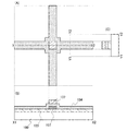
200 基板
202 第1の導電膜
204 第1のレジスト
206 第1のレジストマスク
208 第1の導電層
210 第1の絶縁膜
212 半導体膜
214 不純物半導体膜
216 第2のレジスト
218 第2のレジストマスク
220 第3のレジストマスク
222 半導体層
224 不純物半導体層
226 第2の導電層
228 保護層
230 第3の導電層
240 第1の絶縁膜
242 半導体膜
246 第2のレジスト
248 第2のレジストマスク
250 第3のレジストマスク
252 半導体層
254 不純物半導体層
256 第2の導電層
258 保護層
260 第3の導電層
200S 基板
206S 第1のレジストマスク
208S 第1の導電層
210S 第1の絶縁膜
212S 半導体膜
214S 不純物半導体膜
216S 第2のレジスト
218S 第2のレジストマスク
220S 第3のレジストマスク
222S 半導体層
224S 不純物半導体層
226S 第2の導電層
228S 保護層
230S 第3の導電層
240S 第1の絶縁膜
242S 半導体膜
246S 第2のレジスト
248S 第2のレジストマスク
250S 第3のレジストマスク
252S 半導体層
254S 不純物半導体層
256S 第2の導電層
258S 保護層
260S 第3の導電層
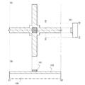
300 基板
302 遮光層
304 第1の絶縁膜
306 第1の導電層
308 第2の絶縁膜
310 半導体層
312 バッファ層
314 不純物半導体層
316 第2の導電層
318 保護層
320 第3の導電層
322 遮光膜
323 第1の絶縁膜
324 第1のレジストマスク
325 第1の導電膜
326 第1の導電膜
327 第1の絶縁層
328 第2のレジストマスク
330 半導体膜
332 バッファ膜
334 不純物半導体膜
336 第3のレジストマスク
338 第4のレジストマスク
340 バッファ膜
342 不純物半導体膜
344 第2の導電膜
346 第5のレジストマスク
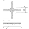
350 基板
352 遮光層
354 第1の絶縁膜
356 第1の導電層
358 第2の絶縁膜
360 半導体層
366 第2の導電層
368 保護層
370 第3の導電層
372 遮光膜
374 第1のレジストマスク
376 第1の導電膜
378 第2のレジストマスク
380 第3のレジストマスク
382 半導体膜
384 バッファ膜
386 不純物半導体膜
388 第4のレジストマスク
390 バッファ膜
392 不純物半導体膜
394 第2の導電膜
396 第5のレジストマスク
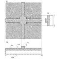
400 基板
402 下地膜
404 半導体層
406 第1の絶縁膜
408 第1の導電膜
410 第2のレジストマスク
412 第3のレジストマスク
414 第1の導電層
416 第2の絶縁膜
418 第2の導電膜
420 第4のレジストマスク
422 第2の導電層
424 第3の絶縁膜
426 第4の絶縁膜
428 第3の導電層
Claims (6)
- 第1の導電膜を形成し、
前記第1の導電膜上に第1のレジストマスクを形成し、
前記第1のレジストマスクを用いて前記第1の導電膜をエッチングすることで、第1の導電層を形成し、
前記第1の導電層を覆って第1の絶縁膜と、半導体膜と、不純物半導体膜と、を下から順に積層して形成し、
前記不純物半導体膜上に第2のレジストマスクを形成し、
前記2のレジストマスクを縮小させて第3のレジストマスクを形成し、
前記第3のレジストマスクを用いて前記半導体膜と前記不純物半導体膜をエッチングすることで、半導体層と不純物半導体層とを形成し、
前記半導体層と前記不純物半導体層を覆って第2の導電層を形成し、
前記第1のレジストマスクと前記第2のレジストマスクとは、同一のフォトマスクまたは同一形状のフォトマスクにより形成することを特徴とする薄膜トランジスタの作製方法。 - 第1の導電膜を形成し、
前記第1の導電膜上に第1のレジストマスクを形成し、
前記第1のレジストマスクを用いて前記第1の導電膜をエッチングすることで、第1の導電層を形成し、
前記第1の導電層を覆って第1の絶縁膜と第1の絶縁膜上の半導体膜を積層して形成し、
前記半導体膜上に第2のレジストマスクを形成し、
前記第2のレジストマスクを縮小させて第3のレジストマスクを形成し、
前記第3のレジストマスクを用いて前記半導体膜をエッチングすることで、半導体層を形成し、
前記半導体層上に、不純物半導体層と前記不純物半導体層上の第2の導電層を形成し、
前記第1のレジストマスクと前記第2のレジストマスクとは、同一のフォトマスクまたは同一形状のフォトマスクにより形成することを特徴とする薄膜トランジスタの作製方法。 - 請求項1または請求項2において、
前記第1の導電層にスリットを設けることを特徴とする薄膜トランジスタの作製方法。 - 請求項1乃至請求項3のいずれか一において、
レジストマスクの縮小は、アッシング処理、酸素プラズマ処理、またはオゾン水による処理によって行われることを特徴とする薄膜トランジスタの作製方法。 - 半導体層上を覆って第1の絶縁膜と前記第1の絶縁膜上の第1の導電膜を形成し、
前記第1の導電膜上に第1のレジストマスクを形成し、
前記第1のレジストマスクを縮小させて第2のレジストマスクを形成し、
前記第2のレジストマスクを用いて前記第1の導電膜をエッチングすることで、第1の導電層を形成し、
前記第2のレジストマスクを除去し、
前記第1の導電層上に第2の絶縁膜と前記第2の絶縁膜上の第2の導電膜を形成し、前記第2の導電膜上に第3のレジストマスクを形成し、
前記第3のレジストマスクを用いて前記第2の導電膜をエッチングすることで、第2の導電層を形成し、
前記第3のレジストマスクを除去し、
前記第1のレジストマスクと前記第3のレジストマスクは、同一のフォトマスクまたは同一形状のフォトマスクにより形成することを特徴とする不揮発性半導体記憶素子の作製方法。 - 請求項5において、
レジストマスクの縮小は、アッシング処理、酸素プラズマ処理、またはオゾン水による処理によって行われることを特徴とする不揮発性半導体記憶素子の作製方法。
Priority Applications (1)
| Application Number | Priority Date | Filing Date | Title |
|---|---|---|---|
| JP2009130819A JP5514474B2 (ja) | 2009-05-29 | 2009-05-29 | 薄膜トランジスタの作製方法、不揮発性半導体記憶素子の作製方法 |
Applications Claiming Priority (1)
| Application Number | Priority Date | Filing Date | Title |
|---|---|---|---|
| JP2009130819A JP5514474B2 (ja) | 2009-05-29 | 2009-05-29 | 薄膜トランジスタの作製方法、不揮発性半導体記憶素子の作製方法 |
Publications (3)
| Publication Number | Publication Date |
|---|---|
| JP2010278320A JP2010278320A (ja) | 2010-12-09 |
| JP2010278320A5 JP2010278320A5 (ja) | 2012-06-21 |
| JP5514474B2 true JP5514474B2 (ja) | 2014-06-04 |
Family
ID=43424995
Family Applications (1)
| Application Number | Title | Priority Date | Filing Date |
|---|---|---|---|
| JP2009130819A Expired - Fee Related JP5514474B2 (ja) | 2009-05-29 | 2009-05-29 | 薄膜トランジスタの作製方法、不揮発性半導体記憶素子の作製方法 |
Country Status (1)
| Country | Link |
|---|---|
| JP (1) | JP5514474B2 (ja) |
Families Citing this family (3)
| Publication number | Priority date | Publication date | Assignee | Title |
|---|---|---|---|---|
| JP5563888B2 (ja) * | 2010-05-12 | 2014-07-30 | 三菱電機株式会社 | 薄膜トランジスタとその製造方法、アクティブマトリックス基板、及び電気光学装置 |
| JP5848918B2 (ja) | 2010-09-03 | 2016-01-27 | 株式会社半導体エネルギー研究所 | 半導体装置の作製方法 |
| JP5667868B2 (ja) * | 2010-12-24 | 2015-02-12 | 株式会社半導体エネルギー研究所 | 半導体装置の作製方法 |
Family Cites Families (8)
| Publication number | Priority date | Publication date | Assignee | Title |
|---|---|---|---|---|
| JPS63313866A (ja) * | 1987-06-17 | 1988-12-21 | Seiko Epson Corp | 半導体装置の製造方法 |
| JPH04277721A (ja) * | 1991-03-06 | 1992-10-02 | Seikosha Co Ltd | 薄膜パターンの形成方法 |
| JPH0613474A (ja) * | 1992-06-26 | 1994-01-21 | Nippon Steel Corp | 半導体装置の製造方法 |
| JPH0822983A (ja) * | 1994-07-05 | 1996-01-23 | Citizen Watch Co Ltd | 半導体装置の製造方法 |
| JPH09127707A (ja) * | 1995-10-30 | 1997-05-16 | Casio Comput Co Ltd | レジストパターンの形成方法 |
| JP3214321B2 (ja) * | 1995-11-03 | 2001-10-02 | トヨタ自動車株式会社 | 薄膜トランジスタ及びその製造方法 |
| JP5105811B2 (ja) * | 2005-10-14 | 2012-12-26 | 株式会社半導体エネルギー研究所 | 表示装置 |
| US7994000B2 (en) * | 2007-02-27 | 2011-08-09 | Semiconductor Energy Laboratory Co., Ltd. | Semiconductor device and method of manufacturing the same |
-
2009
- 2009-05-29 JP JP2009130819A patent/JP5514474B2/ja not_active Expired - Fee Related
Also Published As
| Publication number | Publication date |
|---|---|
| JP2010278320A (ja) | 2010-12-09 |
Similar Documents
| Publication | Publication Date | Title |
|---|---|---|
| US9543443B2 (en) | Thin film transistor assembly, array substrate method of manufacturing the same, and display device | |
| JP5209146B2 (ja) | 半導体装置およびその製造方法 | |
| US11296074B2 (en) | Electrostatic protection circuit and manufacturing method thereof, array substrate and display apparatus | |
| KR101078358B1 (ko) | 비정질 실리콘 박막 트랜지스터 및 이를 제조하는 방법 | |
| US9437627B2 (en) | Thin film transistor and manufacturing method thereof | |
| JP6503459B2 (ja) | 半導体装置及びその製造方法 | |
| EP3093888B1 (en) | Method of fabricating a thin film transistor | |
| US9006059B2 (en) | CMOS transistor and method for fabricating the same | |
| US9117915B2 (en) | Thin film transistor, pixel structure and method for fabricating the same | |
| WO2017070868A1 (zh) | N型tft的制作方法 | |
| US20170329163A1 (en) | Preparation method for thin film transistor, preparation method for array substrate, array substrate, and display apparatus | |
| EP3449498B1 (en) | Thin film transistor, display apparatus having the same, and fabricating method thereof | |
| CN105355588A (zh) | Tft阵列基板的制备方法、tft阵列基板及显示装置 | |
| CN108565247B (zh) | Ltps tft基板的制作方法及ltps tft基板 | |
| WO2016008197A1 (zh) | 阵列基板及其制造方法 | |
| JP5514474B2 (ja) | 薄膜トランジスタの作製方法、不揮発性半導体記憶素子の作製方法 | |
| US10957713B2 (en) | LTPS TFT substrate and manufacturing method thereof | |
| CN108511464B (zh) | Cmos型ltps tft基板的制作方法 | |
| US20160358944A1 (en) | Oxide Semiconductor TFT Array Substrate and Method for Manufacturing the Same | |
| TWI573226B (zh) | 薄膜電晶體基板及其製作方法 | |
| KR101200237B1 (ko) | 디스플레이용 박막 트랜지스터 및 이의 제조방법 | |
| JP5558222B2 (ja) | 薄膜トランジスタ基板の製造方法 | |
| JP4708099B2 (ja) | トランジスタ製造用マスクおよびこれを用いてトランジスタを製造する方法 | |
| US8835206B2 (en) | Pixel structure, array substrate and method of fabricating the same | |
| CN106298951B (zh) | 薄膜晶体管的制作方法 |
Legal Events
| Date | Code | Title | Description |
|---|---|---|---|
| A521 | Request for written amendment filed |
Free format text: JAPANESE INTERMEDIATE CODE: A523 Effective date: 20120508 |
|
| A621 | Written request for application examination |
Free format text: JAPANESE INTERMEDIATE CODE: A621 Effective date: 20120508 |
|
| A977 | Report on retrieval |
Free format text: JAPANESE INTERMEDIATE CODE: A971007 Effective date: 20131114 |
|
| A131 | Notification of reasons for refusal |
Free format text: JAPANESE INTERMEDIATE CODE: A131 Effective date: 20131119 |
|
| A521 | Request for written amendment filed |
Free format text: JAPANESE INTERMEDIATE CODE: A523 Effective date: 20131128 |
|
| TRDD | Decision of grant or rejection written | ||
| A01 | Written decision to grant a patent or to grant a registration (utility model) |
Free format text: JAPANESE INTERMEDIATE CODE: A01 Effective date: 20140325 |
|
| A61 | First payment of annual fees (during grant procedure) |
Free format text: JAPANESE INTERMEDIATE CODE: A61 Effective date: 20140331 |
|
| R150 | Certificate of patent or registration of utility model |
Ref document number: 5514474 Country of ref document: JP Free format text: JAPANESE INTERMEDIATE CODE: R150 |
|
| R250 | Receipt of annual fees |
Free format text: JAPANESE INTERMEDIATE CODE: R250 |
|
| R250 | Receipt of annual fees |
Free format text: JAPANESE INTERMEDIATE CODE: R250 |
|
| R250 | Receipt of annual fees |
Free format text: JAPANESE INTERMEDIATE CODE: R250 |
|
| R250 | Receipt of annual fees |
Free format text: JAPANESE INTERMEDIATE CODE: R250 |
|
| R250 | Receipt of annual fees |
Free format text: JAPANESE INTERMEDIATE CODE: R250 |
|
| R250 | Receipt of annual fees |
Free format text: JAPANESE INTERMEDIATE CODE: R250 |
|
| LAPS | Cancellation because of no payment of annual fees |