JP5487635B2 - 電気光学装置および電子機器 - Google Patents
電気光学装置および電子機器 Download PDFInfo
- Publication number
- JP5487635B2 JP5487635B2 JP2009029917A JP2009029917A JP5487635B2 JP 5487635 B2 JP5487635 B2 JP 5487635B2 JP 2009029917 A JP2009029917 A JP 2009029917A JP 2009029917 A JP2009029917 A JP 2009029917A JP 5487635 B2 JP5487635 B2 JP 5487635B2
- Authority
- JP
- Japan
- Prior art keywords
- electro
- backlight unit
- liquid crystal
- frame
- panel
- Prior art date
- Legal status (The legal status is an assumption and is not a legal conclusion. Google has not performed a legal analysis and makes no representation as to the accuracy of the status listed.)
- Expired - Fee Related
Links
- 239000000758 substrate Substances 0.000 claims description 104
- 239000004973 liquid crystal related substance Substances 0.000 description 95
- 239000010408 film Substances 0.000 description 9
- 238000004519 manufacturing process Methods 0.000 description 9
- 239000003566 sealing material Substances 0.000 description 7
- 238000007689 inspection Methods 0.000 description 6
- 230000007547 defect Effects 0.000 description 5
- 239000002184 metal Substances 0.000 description 5
- 229910052751 metal Inorganic materials 0.000 description 5
- 238000000034 method Methods 0.000 description 5
- 238000012360 testing method Methods 0.000 description 4
- 239000002390 adhesive tape Substances 0.000 description 3
- 239000000470 constituent Substances 0.000 description 3
- 239000000463 material Substances 0.000 description 3
- 239000011159 matrix material Substances 0.000 description 3
- 239000000853 adhesive Substances 0.000 description 2
- 230000001070 adhesive effect Effects 0.000 description 2
- 238000009792 diffusion process Methods 0.000 description 2
- 239000011521 glass Substances 0.000 description 2
- 238000005286 illumination Methods 0.000 description 2
- 238000002347 injection Methods 0.000 description 2
- 239000007924 injection Substances 0.000 description 2
- 230000002452 interceptive effect Effects 0.000 description 2
- 230000001678 irradiating effect Effects 0.000 description 2
- WABPQHHGFIMREM-UHFFFAOYSA-N lead(0) Chemical compound [Pb] WABPQHHGFIMREM-UHFFFAOYSA-N 0.000 description 2
- 238000012423 maintenance Methods 0.000 description 2
- 238000012856 packing Methods 0.000 description 2
- 229920001721 polyimide Polymers 0.000 description 2
- 239000010453 quartz Substances 0.000 description 2
- 238000000926 separation method Methods 0.000 description 2
- VYPSYNLAJGMNEJ-UHFFFAOYSA-N silicon dioxide Inorganic materials O=[Si]=O VYPSYNLAJGMNEJ-UHFFFAOYSA-N 0.000 description 2
- 239000010409 thin film Substances 0.000 description 2
- RYGMFSIKBFXOCR-UHFFFAOYSA-N Copper Chemical compound [Cu] RYGMFSIKBFXOCR-UHFFFAOYSA-N 0.000 description 1
- 206010040844 Skin exfoliation Diseases 0.000 description 1
- 239000011889 copper foil Substances 0.000 description 1
- 230000002950 deficient Effects 0.000 description 1
- 230000000694 effects Effects 0.000 description 1
- 238000000605 extraction Methods 0.000 description 1
- 239000012528 membrane Substances 0.000 description 1
- 230000003287 optical effect Effects 0.000 description 1
- 238000005192 partition Methods 0.000 description 1
- 230000002093 peripheral effect Effects 0.000 description 1
- 229920005668 polycarbonate resin Polymers 0.000 description 1
- 239000004431 polycarbonate resin Substances 0.000 description 1
- 238000003908 quality control method Methods 0.000 description 1
- 239000000565 sealant Substances 0.000 description 1
- 229910052710 silicon Inorganic materials 0.000 description 1
- 239000010703 silicon Substances 0.000 description 1
- 229910000679 solder Inorganic materials 0.000 description 1
- 229910001220 stainless steel Inorganic materials 0.000 description 1
- 239000010935 stainless steel Substances 0.000 description 1
- 229920003002 synthetic resin Polymers 0.000 description 1
- 239000000057 synthetic resin Substances 0.000 description 1
Images


Landscapes
- Liquid Crystal (AREA)
- Planar Illumination Modules (AREA)
- Devices For Indicating Variable Information By Combining Individual Elements (AREA)
Description
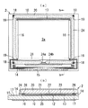
上記の本発明に係る電気光学装置およびそれを用いた電子機器は、以下の構成としたものである。すなわち、本発明による電気光学装置は、電気光学パネルと、該電気光学パネルに対向して配置されたバックライトユニットとが実装ケースに収容された電気光学装置であって、前記電気光学パネルに電気的に接続された第1の可撓性基板と、前記バックライトユニットに電気的に接続された第2の可撓性基板とを備え、前記実装ケースは、前記電気光学パネル及び前記バックライトユニットの側方に設けられた側壁を有し、前記側壁は、前記電気光学パネルの側方に設けられた第1切欠部と、前記バックライトユニットの側方に設けられた第2切欠部とを有し、前記第1の可撓性基板は、前記側壁に設けられた第1切欠部から引き出されており、前記第2の可撓性基板は、前記側壁に設けられた第2切欠部から前記第1の可撓性基板と同一方向に引き出されることを特徴とする。
Claims (6)
- 電気光学パネルと、該電気光学パネルに対向して配置されたバックライトユニットとが実装ケースに収容された電気光学装置であって、
前記電気光学パネルに電気的に接続された第1の可撓性基板と、前記バックライトユニットに電気的に接続された第2の可撓性基板とを備え、
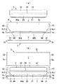
前記実装ケースは、前記電気光学パネル及び前記バックライトユニットを収容するフレームと、前記電気光学パネルの一方の面を覆い前記バックライトユニットと係合されるカバーと、を含み、
前記フレームは、前記電気光学パネル及び前記バックライトユニットの側方に設けられた第1の側壁及び前記第1の側壁に対向するように配置された第2の側壁を有し、前記第1の側壁は、前記電気光学パネルの側方に形成された第1切欠部と、前記バックライトユニットの側方に形成された第2切欠部とを有し、
前記第1の可撓性基板は、前記第1の側壁に形成された第1切欠部から引き出されており、前記第2の可撓性基板は、前記第1の側壁に形成された第2切欠部から前記第1の可撓性基板と同一方向に引き出され、
前記カバーは、前記第1の側壁と前記第2の側壁との間に収まるように配置されることを特徴とする電気光学装置。 - 前記実装ケースは、前記電気光学パネルと前記バックライトユニットとを互いに対向配置させた状態で支持するためのフレームを備えていることを特徴とする請求項1に記載の電気光学装置。
- 前記フレームは、方形枠状に形成されていることを特徴とする請求項2に記載の電気光学装置。
- 前記第1及び第2の可撓性基板の実装ケースからの引き出し長さは、そのいずれか一方が他方よりも長く形成されていることを特徴とする請求項1〜3のいずれかに記載の電気光学装置。
- 前記第1及び第2の可撓性基板の幅は、前記実装ケースの幅よりも狭く形成されていることを特徴とする請求項1〜4のいずれかに記載の電気光学装置。
- 請求項1〜5のいずれかに記載の電気光学装置を有することを特徴とする電子機器。
Priority Applications (1)
| Application Number | Priority Date | Filing Date | Title |
|---|---|---|---|
| JP2009029917A JP5487635B2 (ja) | 2009-02-12 | 2009-02-12 | 電気光学装置および電子機器 |
Applications Claiming Priority (1)
| Application Number | Priority Date | Filing Date | Title |
|---|---|---|---|
| JP2009029917A JP5487635B2 (ja) | 2009-02-12 | 2009-02-12 | 電気光学装置および電子機器 |
Related Child Applications (1)
| Application Number | Title | Priority Date | Filing Date |
|---|---|---|---|
| JP2013269348A Division JP5708783B2 (ja) | 2013-12-26 | 2013-12-26 | 電気光学装置、電子機器、及び支持部材 |
Publications (3)
| Publication Number | Publication Date |
|---|---|
| JP2010186035A JP2010186035A (ja) | 2010-08-26 |
| JP2010186035A5 JP2010186035A5 (ja) | 2012-02-16 |
| JP5487635B2 true JP5487635B2 (ja) | 2014-05-07 |
Family
ID=42766726
Family Applications (1)
| Application Number | Title | Priority Date | Filing Date |
|---|---|---|---|
| JP2009029917A Expired - Fee Related JP5487635B2 (ja) | 2009-02-12 | 2009-02-12 | 電気光学装置および電子機器 |
Country Status (1)
| Country | Link |
|---|---|
| JP (1) | JP5487635B2 (ja) |
Family Cites Families (5)
| Publication number | Priority date | Publication date | Assignee | Title |
|---|---|---|---|---|
| JPH1164830A (ja) * | 1997-08-21 | 1999-03-05 | Citizen Watch Co Ltd | 液晶表示装置 |
| JP3436240B2 (ja) * | 1999-07-14 | 2003-08-11 | 日本電気株式会社 | フラットパネル型表示装置 |
| JP2007233251A (ja) * | 2006-03-03 | 2007-09-13 | Mitsubishi Electric Corp | 表示装置 |
| JP3129206U (ja) * | 2006-11-27 | 2007-02-08 | 船井電機株式会社 | 液晶モジュール |
| JP5076669B2 (ja) * | 2007-06-20 | 2012-11-21 | エプソンイメージングデバイス株式会社 | 電気光学装置、保持枠体及び電子機器 |
-
2009
- 2009-02-12 JP JP2009029917A patent/JP5487635B2/ja not_active Expired - Fee Related
Also Published As
| Publication number | Publication date |
|---|---|
| JP2010186035A (ja) | 2010-08-26 |
Similar Documents
| Publication | Publication Date | Title |
|---|---|---|
| JP5386941B2 (ja) | 電気光学装置及びその製造方法並びに電子機器 | |
| US8319109B2 (en) | Electro-optical device and electronic apparatus | |
| US7667798B2 (en) | Liquid crystal display device | |
| JP4244942B2 (ja) | 液晶装置、照明装置、および電子機器 | |
| JP5257010B2 (ja) | 電気光学装置及び電子機器 | |
| JP5458549B2 (ja) | 電気光学装置及び電子機器 | |
| JP5262601B2 (ja) | 電気光学装置および電子機器 | |
| CN107664863B (zh) | 液晶显示装置 | |
| JP2010096801A (ja) | 電気光学装置及び電子機器 | |
| JP2004341216A (ja) | 電気光学装置用基板及びその製造方法、並びに該電気光学装置用基板を備えた電気光学装置及び電子機器 | |
| JP2009020272A (ja) | 電気光学装置及び電子機器 | |
| US9069199B2 (en) | Liquid crystal module and liquid crystal display device including the same | |
| JP5487635B2 (ja) | 電気光学装置および電子機器 | |
| JP5708783B2 (ja) | 電気光学装置、電子機器、及び支持部材 | |
| JP7126844B2 (ja) | 連結表示装置 | |
| JP5458550B2 (ja) | 電気光学装置および電子機器 | |
| JP5257011B2 (ja) | 電気光学装置および電子機器 | |
| JP2010073389A (ja) | 面状光源装置及び液晶表示装置 | |
| JP5417808B2 (ja) | 電気光学装置及び電子機器 | |
| KR101777127B1 (ko) | 평판 표시장치 및 그 조립방법 | |
| KR20070056780A (ko) | 액정표시장치 | |
| JP2007192853A (ja) | 電気光学装置の製造方法 | |
| JP2005326473A (ja) | 電気光学装置の製造方法、照明装置の製造方法、電気光学装置、照明装置及び電子機器 | |
| JPH08278511A (ja) | 回路基板を有する装置および液晶表示装置 | |
| JP4857605B2 (ja) | 電気光学装置、電気光学装置の製造方法及び電子機器 |
Legal Events
| Date | Code | Title | Description |
|---|---|---|---|
| A521 | Request for written amendment filed |
Free format text: JAPANESE INTERMEDIATE CODE: A523 Effective date: 20111221 |
|
| A621 | Written request for application examination |
Free format text: JAPANESE INTERMEDIATE CODE: A621 Effective date: 20111221 |
|
| A977 | Report on retrieval |
Free format text: JAPANESE INTERMEDIATE CODE: A971007 Effective date: 20121121 |
|
| A131 | Notification of reasons for refusal |
Free format text: JAPANESE INTERMEDIATE CODE: A131 Effective date: 20121127 |
|
| A02 | Decision of refusal |
Free format text: JAPANESE INTERMEDIATE CODE: A02 Effective date: 20131001 |
|
| A521 | Request for written amendment filed |
Free format text: JAPANESE INTERMEDIATE CODE: A523 Effective date: 20131226 |
|
| A911 | Transfer to examiner for re-examination before appeal (zenchi) |
Free format text: JAPANESE INTERMEDIATE CODE: A911 Effective date: 20140109 |
|
| TRDD | Decision of grant or rejection written | ||
| A01 | Written decision to grant a patent or to grant a registration (utility model) |
Free format text: JAPANESE INTERMEDIATE CODE: A01 Effective date: 20140128 |
|
| A61 | First payment of annual fees (during grant procedure) |
Free format text: JAPANESE INTERMEDIATE CODE: A61 Effective date: 20140210 |
|
| R150 | Certificate of patent or registration of utility model |
Ref document number: 5487635 Country of ref document: JP Free format text: JAPANESE INTERMEDIATE CODE: R150 |
|
| S531 | Written request for registration of change of domicile |
Free format text: JAPANESE INTERMEDIATE CODE: R313531 |
|
| R350 | Written notification of registration of transfer |
Free format text: JAPANESE INTERMEDIATE CODE: R350 |
|
| LAPS | Cancellation because of no payment of annual fees |