JP5487635B2 - Electro-optical device and electronic apparatus - Google Patents
Electro-optical device and electronic apparatus Download PDFInfo
- Publication number
- JP5487635B2 JP5487635B2 JP2009029917A JP2009029917A JP5487635B2 JP 5487635 B2 JP5487635 B2 JP 5487635B2 JP 2009029917 A JP2009029917 A JP 2009029917A JP 2009029917 A JP2009029917 A JP 2009029917A JP 5487635 B2 JP5487635 B2 JP 5487635B2
- Authority
- JP
- Japan
- Prior art keywords
- electro
- backlight unit
- liquid crystal
- frame
- panel
- Prior art date
- Legal status (The legal status is an assumption and is not a legal conclusion. Google has not performed a legal analysis and makes no representation as to the accuracy of the status listed.)
- Expired - Fee Related
Links
Images


Landscapes
- Liquid Crystal (AREA)
- Planar Illumination Modules (AREA)
- Devices For Indicating Variable Information By Combining Individual Elements (AREA)
Description
本発明は、液晶装置等の電気光学装置およびそれを用いた電子機器に関する。更に詳しくは、液晶パネル等の電気光学パネルと、その電気光学パネルに光を照射するためのバックライトユニットとを備えた電気光学装置およびそれを用いた電子機器に関する。 The present invention relates to an electro-optical device such as a liquid crystal device and an electronic apparatus using the same. More particularly, the present invention relates to an electro-optical device including an electro-optical panel such as a liquid crystal panel and a backlight unit for irradiating the electro-optical panel with light, and an electronic apparatus using the same.
従来、例えば液晶装置等の電気光学装置は、コンピュータや携帯電話その他各種電子機器の表示部などとして用いられ、特に液晶装置は軽量・薄型で消費電力も少ないことから各種電子機器の表示部として広く利用されている。また上記のような液晶装置等の電気光学装置においては、液晶パネル等の電気光学パネルの背面側に、いわゆるバックライトを備えたものが多く用いられている。 2. Description of the Related Art Conventionally, electro-optical devices such as liquid crystal devices have been used as display units for computers, mobile phones, and other various electronic devices, and in particular, liquid crystal devices are widely used as display units for various electronic devices because they are lightweight, thin, and consume less power. It's being used. In the electro-optical device such as the liquid crystal device as described above, a device having a so-called backlight on the back side of the electro-optical panel such as a liquid crystal panel is often used.
この種のバックライトは、照明用の光源と、その光源からの光を電気光学パネルに導くための導光板や光拡散板などを1つのユニットとして構成するのが一般的であり、そのようなユニット化したバックライトユニットを電気光学パネルの背面側に対向配置して該バックライトユニットからの光を上記パネルに背面側から照射することによって該パネルの正面側の画素領域に所望の画像等を表示するものである。 This type of backlight generally comprises a light source for illumination and a light guide plate or light diffusing plate for guiding light from the light source to the electro-optical panel as one unit. A unitized backlight unit is disposed opposite to the back side of the electro-optic panel, and the light from the backlight unit is irradiated to the panel from the back side, whereby a desired image or the like is applied to the pixel area on the front side of the panel. To display.
このようなバックライトユニットを備えた電気光学パネルを、1つの電気光学装置として構成する場合、もしくは各種の電子機器に実装する場合には、上記パネルとバックライトユニットとを実装ケース内に収容するのが一般的であり、例えば下記特許文献1には、光源45や光拡散板44等を上下ケース41・42間に配置してなるバックライトユニット(照明装置)40を、液晶パネル30及びその駆動用の回路基板50とともに、前面枠21とシールドカバー22とからなる実装ケース内に収容した構成が開示されている。
When an electro-optical panel including such a backlight unit is configured as one electro-optical device or mounted on various electronic devices, the panel and the backlight unit are accommodated in a mounting case. For example, in
しかし、上記特許文献1のものは、液晶パネル30に接続したフレキシブルプリント配線基板31と、バックライトユニット40の光源45のリード線47とを互いに反対方向に引き出し、フレキシブルプリント配線基板31の他端を、実装ケース内に収容した回路基板50にコネクタ503を介して接続すると共に、その回路基板50の外部接続用コネクタ502に接続したフレキシブル接続線503を、実装ケースの背面側のシールドカバー22に形成した開口222から実装ケースの背面側に引き出した構成である。また上記リード線47は光拡散板44の周囲にコ字形に配置した光源45の両端部から下ケース42の背面側に導いた後、実装ケースのフレキシブルプリント配線基板31と反対側の側面に形成した孔から上記配線基板31と反対側に引き出した構成である。
However, in the above-mentioned
そのため、上記の液晶装置を組立てる際には、液晶パネル30及びバックライトユニット40に接続される配線接続部材の引き回しや接続作業が煩雑かつ面倒で、それらの組み付け作業や接続作業に多大な労力と時間を要し、製造コストが増大するだけでなく、製造時の品質管理や製造後の保守点検およびメンテナンスがしずらく、またリワークやリペアも困難である等の不具合がある。
Therefore, when assembling the above liquid crystal device, the wiring connection members connected to the
一方、下記特許文献2には、導光板とLEDパッケージ等からなるバックライトユニットを、液晶パネルの背面側に配置した状態で、実装ケースとしての略箱状の金属フレーム内に収容し、液晶パネルに接続したパネル駆動用のFPC(Flexible Printed Circuit)を金属フレーム内から外部に引き出すと共に、LEDパッケージの一対の電源端子を金属フレームに形成した開口部から外部に引き出し、その各電源端子の端部を金属フレームから引き出したFPC上の接続端子に半田付けして接続することが提案されている。
On the other hand, in
しかし、上記のようにLEDパッケージの電源端子を液晶パネル駆動用のFPCに接続するものは、例えば液晶パネルやLEDパッケージに電気的な故障や欠陥がある場合に、その発見が難しい。例えば通電時にバックライトが点灯しなかった場合、バックライトの故障か配線接続の不具合か即断できない場合がある。また液晶パネルまたはLEDパッケージのいずれかに故障や欠陥が見つかって、リワークやリペアを行う際には、電源端子とFPCとを分離するのが困難で無理に離すと、FPC上の配線が基板から剥離してしまう等のおそれがある。 However, it is difficult to find the case where the power supply terminal of the LED package is connected to the FPC for driving the liquid crystal panel as described above, for example, when the liquid crystal panel or the LED package has an electrical failure or defect. For example, if the backlight does not light up when energized, it may not be possible to immediately determine whether the backlight is faulty or the wiring connection is defective. In addition, when a failure or defect is found in either the liquid crystal panel or the LED package and it is difficult to separate the power supply terminal and the FPC when performing rework or repair, the wiring on the FPC will be disconnected from the substrate. There is a risk of peeling.
本発明は上記の問題点に鑑みて提案されたもので、液晶パネル等の電気光学パネルと、バックライトユニットにそれぞれ接続したFPC等の可撓性基板の製造時の引き出しや組み付け作業、及び電気光学パネルやバックライトユニットの電気的な故障や欠陥の発見およびリワークやリペアが簡単で容易・安価に製造することのできる電気光学装置およびそれを用いた電子機器を提供することを目的とする。 The present invention has been proposed in view of the above-described problems, and includes drawing and assembling work during manufacturing of an electro-optical panel such as a liquid crystal panel and a flexible substrate such as an FPC connected to a backlight unit, and electric It is an object of the present invention to provide an electro-optical device and an electronic apparatus using the same, which can easily and inexpensively manufacture an electrical failure or defect of an optical panel or a backlight unit, and can be easily reworked or repaired.
本発明の一態様の電気光学装置は、電気光学パネルと、該電気光学パネルに対向して配置されたバックライトユニットとが実装ケースに収容された電気光学装置であって、前記電気光学パネルに電気的に接続された第1の可撓性基板と、前記バックライトユニットに電気的に接続された第2の可撓性基板とを備え、前記実装ケースは、前記電気光学パネル及び前記バックライトユニットを収容するフレームと、前記電気光学パネルの一方の面を覆い前記バックライトユニットと係合されるカバーと、を含み、前記フレームは、前記電気光学パネル及び前記バックライトユニットの側方に設けられた第1の側壁及び前記第1の側壁に対向するように配置された第2の側壁を有し、前記第1の側壁は、前記電気光学パネルの側方に形成された第1切欠部と、前記バックライトユニットの側方に形成された第2切欠部とを有し、前記第1の可撓性基板は、前記第1の側壁に形成された第1切欠部から引き出されており、前記第2の可撓性基板は、前記第1の側壁に形成された第2切欠部から前記第1の可撓性基板と同一方向に引き出され、前記カバーは、前記第1の側壁と前記第2の側壁との間に収まるように配置されることを特徴とする。
上記の本発明に係る電気光学装置およびそれを用いた電子機器は、以下の構成としたものである。すなわち、本発明による電気光学装置は、電気光学パネルと、該電気光学パネルに対向して配置されたバックライトユニットとが実装ケースに収容された電気光学装置であって、前記電気光学パネルに電気的に接続された第1の可撓性基板と、前記バックライトユニットに電気的に接続された第2の可撓性基板とを備え、前記実装ケースは、前記電気光学パネル及び前記バックライトユニットの側方に設けられた側壁を有し、前記側壁は、前記電気光学パネルの側方に設けられた第1切欠部と、前記バックライトユニットの側方に設けられた第2切欠部とを有し、前記第1の可撓性基板は、前記側壁に設けられた第1切欠部から引き出されており、前記第2の可撓性基板は、前記側壁に設けられた第2切欠部から前記第1の可撓性基板と同一方向に引き出されることを特徴とする。
An electro-optical device according to an aspect of the present invention is an electro-optical device in which an electro-optical panel and a backlight unit arranged to face the electro-optical panel are accommodated in a mounting case. A first flexible board electrically connected; and a second flexible board electrically connected to the backlight unit; and the mounting case includes the electro-optical panel and the backlight. A frame that accommodates the unit, and a cover that covers one surface of the electro-optical panel and engages with the backlight unit, and the frame is provided on a side of the electro-optical panel and the backlight unit. A first side wall formed on the side of the electro-optic panel. The first side wall is disposed on the side of the electro-optic panel. And a second cutout formed on a side of the backlight unit, and the first flexible substrate is pulled out from the first cutout formed on the first side wall. The second flexible substrate is pulled out in the same direction as the first flexible substrate from a second notch formed in the first side wall, and the cover is It arrange | positions so that it may fit between a side wall and the said 2nd side wall, It is characterized by the above-mentioned.
The electro-optical device according to the present invention and the electronic apparatus using the same are configured as follows. In other words, the electro-optical device according to the present invention is an electro-optical device in which an electro-optical panel and a backlight unit arranged to face the electro-optical panel are accommodated in a mounting case. A first flexible substrate connected to the backlight unit and a second flexible substrate electrically connected to the backlight unit, and the mounting case includes the electro-optical panel and the backlight unit. A side wall provided on the side of the electro-optic panel, and the side wall includes a first notch provided on the side of the electro-optical panel and a second notch provided on the side of the backlight unit. And the first flexible substrate is pulled out from a first notch provided in the side wall, and the second flexible substrate is extracted from a second notch provided in the side wall. Same as the first flexible substrate Characterized in that it is drawn to the direction.
上記のように電気光学パネルに接続された第1の可撓性基板と、バックライトユニットに接続された第2の可撓性基板とを実装ケースからそれぞれ同一方向に引き出されるようにしたので、例えば上記電気光学装置を製造する際には、上記第1及び第2の可撓性基板をそれぞれ個別に引き出して接続したり、組付けることができる。また電気光学パネルやバックライトユニットの電気的な故障や欠陥の発見が容易であり、しかもリワークやリペアが簡単で容易・安価に製造することが可能となる。 As described above, the first flexible substrate connected to the electro-optical panel and the second flexible substrate connected to the backlight unit are each drawn out from the mounting case in the same direction. For example, when the electro-optical device is manufactured, the first and second flexible substrates can be individually drawn out and connected or assembled. In addition, it is easy to find an electrical failure or defect in the electro-optical panel or the backlight unit, and it is possible to easily and inexpensively manufacture rework and repair.
上記第1及び第2の可撓性基板の実装ケースからの引き出し位置は適宜であるが、実装ケースの一側面から引き出されるようにするとよく、そのようにすると、製造時の可撓性基板の引き出し作業や検査や試験および電子機器への接続や組付け作業を実装ケースの一側面側のみで容易に行うことが可能となる。 The position where the first and second flexible substrates are pulled out from the mounting case is appropriate, but it is preferable that the first flexible substrate is pulled out from one side surface of the mounting case. It is possible to easily perform the drawing work, inspection, testing, connection to the electronic device, and assembly work only on one side of the mounting case.
上記実装ケースの構成も適宜であるが、電気光学パネルとバックライトユニットとを互いに対向配置させた状態で支持するためのフレームを備えるとよく、そのようなフレームを備えると、電気光学パネルとバックライトユニットとを互いに対向配置させた状態で良好に支持させることができる。 Although the configuration of the mounting case is also appropriate, it is preferable to provide a frame for supporting the electro-optical panel and the backlight unit in a state of being opposed to each other. It is possible to favorably support the light unit in a state where the light units are arranged opposite to each other.
上記フレームは方形枠状に形成されたものが望ましく、このような方形枠状のフレームを用いると、その方形枠状のフレームの中央部分の開口部を介してバックライトユニットからの光を電気光学パネルに照射することができる。 The frame is preferably formed in a rectangular frame shape. When such a rectangular frame frame is used, the light from the backlight unit is electro-optically transmitted through the opening in the central portion of the rectangular frame frame. The panel can be irradiated.
また上記第1及び第2の可撓性基板の実装ケースからの引き出し長さは、そのいずれか一方が他方よりも長く形成されているのが望ましい。このようにいずれか一方の引き出し長さが他方よりも長く形成されていると、その第1の可撓性基板と第2の可撓性基板とを、外部の電源や制御回路等に接続する際に、各々別々に容易に接続できると共に、その接続時に上記両可撓性基板が互いに干渉したり、混線することなく、容易・迅速に、かつ良好に接続することが可能となる。 In addition, it is desirable that one of the first and second flexible substrates to be pulled out from the mounting case is longer than the other. When either one of the drawer lengths is longer than the other, the first flexible substrate and the second flexible substrate are connected to an external power source, a control circuit, or the like. In this case, each of the flexible substrates can be easily connected separately, and the flexible substrates can be easily, quickly and satisfactorily connected without interfering with each other or being mixed.
さらに、上記第1及び第2の可撓性基板の幅は、実装ケースの幅よりも狭く形成されているとよく、そのようにすると、例えば電気光学装置の製造時または検査時にトレー等に載置する際、もしくは製品を梱包する際に、嵩張ることがなく、多数の電気光学装置を整然と載置または梱包することができる。また第1及び第2の可撓性基板が実装ケースよりも幅方向外方に飛び出して他物と接触したり、それによって他物や可撓性基板上の配線が損傷もしくは断線するのを未然に防止することができる。 Furthermore, the width of the first and second flexible substrates is preferably formed narrower than the width of the mounting case. In such a case, for example, the first and second flexible substrates are mounted on a tray or the like during manufacture or inspection of the electro-optical device. When placing or packing a product, a large number of electro-optical devices can be placed or packed in an orderly manner without being bulky. In addition, it is possible to prevent the first and second flexible boards from protruding outward in the width direction from the mounting case to come into contact with other objects, thereby causing damage to or damage to other objects and wiring on the flexible board. Can be prevented.
また本発明による電子機器は、上記のような電気光学装置を有することを特徴とする。上記のような電気光学装置を有することで、電子機器の構成が簡略化されると共に、部品点数および組立工数が削減され、容易・安価に製造することが可能となる。 An electronic apparatus according to the present invention includes the electro-optical device as described above. By including the electro-optical device as described above, the configuration of the electronic device is simplified, the number of parts and the number of assembly steps are reduced, and the device can be easily and inexpensively manufactured.
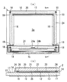
以下、本発明を液晶装置に適用した場合を例にして本発明による電気光学装置を、図に示す実施形態に基づいて具体的に説明する。図1は本発明による電気光学装置としての液晶装置の一実施形態を示す斜視図、図2(a)は上記液晶装置の一実施形態を示す平面図、同図(b)はその側面図、図3、図4及び図5はそれぞれ図2におけるA−A、B−B及びC−C断面図である。 Hereinafter, an electro-optical device according to the present invention will be specifically described based on an embodiment shown in the drawings, taking the case where the present invention is applied to a liquid crystal device as an example. FIG. 1 is a perspective view showing an embodiment of a liquid crystal device as an electro-optical device according to the present invention, FIG. 2A is a plan view showing an embodiment of the liquid crystal device, and FIG. 3, 4 and 5 are sectional views taken along lines AA, BB and CC in FIG. 2, respectively.
本実施形態の液晶装置1は、図1〜図5に示すように電気光学パネルとしての液晶パネル2と、その液晶パネル2の背面側に配設されるバックライトユニット3とを、実装ケース内に収容するようにしたもので、その実装ケースは、本実施形態においては液晶パネル2とバックライトユニット3とを対向配置した状態で嵌合保持する保持部材であるフレーム4と、そのフレーム4に嵌合保持させた液晶パネル2の外面側(バックライトユニット3と反対側)を覆うようにして配設される遮光部材を兼ねるカバー5とよりなる。
As shown in FIGS. 1 to 5, the
上記フレーム4は、本実施形態においてはポリカーボネイト樹脂等の合成樹脂により図1〜図5に示すように全体的にやや扁平な直方体状で、周辺部に平面略方形枠状の側壁部41〜43を有し、その内方に、中央部に透光用の開口部44aを有する仕切板状の支持部44を一体に設けた断面略H字形に形成され、そのH字形フレーム4の一方の凹部(図の場合は上記支持部44よりも上側の凹部)40a内に液晶パネル2を、他方の凹部(図の場合は上記支持部44よりも下側の凹部)40b内にバックライトユニット3をそれぞれ嵌合保持させて収容するようにしたものである。
In the present embodiment, the
上記液晶パネル2及びバックライトユニット3は必要に応じて接着材や両面接着テープ等でフレーム4に固着してもよく、本実施形態においては液晶パネル2はフレーム4に接着材で固定されているが、図には省略した。また上記バックライトユニット3は、液晶パネル2に対して所定の領域以外に光が照射されるのを防ぐための遮光膜を兼ねる略方形枠状の両面接着テープ31を介してフレーム4の支持部44の一方の面(図の場合は下面)に固着した構成である。
The
カバー5は、本実施形態においてはステンレス等の金属板により、フレーム4内に収容した液晶パネル2の一方の面(図の場合は上面)を覆う平面部51と、その平面部51の幅方向(図4及び図5において左右方向)両端部に該平面部51と略直角に屈曲形成した対向面部52・52とからなる断面コ字形(チャンネル型)に形成され、上記平面部51で液晶パネル2のバックライトユニット3と反対側の面を覆い、上記対向面部52・52で、それぞれフレーム4の互いに対向する側壁部43・43の外面の一部を覆うように構成されている。上記各対向面部52・52は、側壁部43・43の外面に接するようにして配置され、平面部51の液晶パネル2の画素領域(表示領域)に対応する位置には、その部分を開口させて形成した表示窓5aが設けられている。
In the present embodiment, the
また上記実施形態においては、図3及び図5に示すように液晶パネル2とバックライトユニット3とをフレーム4に嵌合保持させた状態で液晶パネル2のバックライトユニット3と反対側の面をカバー5で覆い、そのカバー5の対向面部52・52をバックライトユニット3に係合させてカバー5とバックライトユニット3との間に液晶パネル2とフレーム4とを保持させる構成であり、上記カバー5の対向面部52・52をバックライトユニット3に係合させる手段として、図の場合は各対向面部52・52に係止孔5cを形成すると共に、その係止孔5cに係合する突起3cをバックライトユニット3の図5で左右両側の端部に、それと一体的に設けたものである。
In the above embodiment, as shown in FIGS. 3 and 5, the
さらに上記各側壁部43・43の外面側には、図2及び図4に示すように上記対向面部52よりも外側方に突出する張り出し部43aが上記各側壁部43と一体に設けられ、その張り出し部43aとの干渉を避けるようにして各対向面部52・52には、それぞれ切り欠き凹部52aが形成されている。また各対向面部52・52の切り欠き凹部52aの両側には、図2(b)に示すように下向きの舌状部52b・52bが一体に設けられ、その各舌状部52bに上記の係止孔5cが設けられている。その係止孔5cが係合する突起3cは、本実施形態においては上記各係止孔5cに対応してバックライトユニット3の図5で左右両側の端部にそれぞれ2つずつ設けられている。その突起3c及び係止孔5cの配置位置や個数は適宜変更可能である。
Further, as shown in FIGS. 2 and 4, a protruding
図2及び図5において、4cは上記各突起3cの近傍のフレーム4の側壁部43・43の外面にそれと一体に設けた案内突起で、その各案内突起4cのほぼ上半部には傾斜面4c1が設けられ、各係止孔5cをバックライトユニット3の突起3cに係合させる際に、舌状部52bの下端側を外方に押し開きながら案内突起4c及び突起3cを乗り越えさせることによって、舌状部52bに設けた係止孔5cに突起3cを係合させる構成である。
2 and 5,
上記フレーム4の互いに対向する側壁部43・43と交差する方向において互いに対向する側壁部(図2及び図3において左右方向に対向する側壁部)41・42には、その対向する側と反対側(外側)の縁部外周に、それぞれフランジ状の突出部41a・42aが形成され、その両突出部41a・42a間に上記カバー5が配置されている。なお、上記各突出部41a・42aは、図2(b)及び図3に示すようにカバー5よりも外方(図で上方)に突出し、かつバックライトユニット3よりも外方(図で下方)に突出するように形成されている。
The
上記液晶パネル2の構成は適宜であるが、本実施形態は画素用のスイッチング素子として薄膜トランジスタを用いたアクティブマトリックス型の液晶パネルを使用したもので、その具体的な構成を図6に基づいて説明する。図6(a)は液晶パネル2の平面図、同図(b)は(a)におけるb−b断面図である。
Although the configuration of the
上記液晶パネル2の薄膜トランジスタは、図6に示す石英やガラスもしくはシリコン等からなる素子基板(TFTアレイ基板)10上に設けられ、その素子基板10に対向してガラスや石英等からなる対向基板20が設けられている。その素子基板10と対向基板20とは、画素領域(画像表示領域)2aの周囲に設けたシール材24により相互に接着固定され、そのシール材24の内側の素子基板10と対向基板20との間に液晶を注入した液晶層25が設けられている。図6において、24aは上記シール材24の一部を欠落させて形成した液晶注入口、24bはその液晶注入口24aを塞ぐ封止材である。
The thin film transistor of the
上記シール材24の外側の領域、すなわち画素領域2aの外側の周辺領域には、不図示のデータ線に画像信号を所定のタイミングで供給することにより該データ線を駆動するデータ線駆動回路14及び外部回路接続端子15が素子基板10の一辺に沿って設けられている。また不図示の走査線に走査信号を所定のタイミングで供給することにより該走査線を駆動する走査線駆動回路16が、上記一辺に隣接する二辺と平行に且つシール材24の内側に設けた遮光膜26に対向する位置において素子基板10上に設けられている。さらに素子基板10の残る一辺には、上記二辺と平行に設けられた走査線駆動回路16の外部回路接続端子15側と反対側をつなぐための複数の配線17が設けられている。
A data
上記シール材24の4つのコーナー部における素子基板10上には上下導通端子19が形成され、素子基板10と対向基板20相互間には、下端が上下導通端子19に接触し、上端が対向電極20に接触する上下導通材18が設けられており、その上下導通材18によって素子基板10と対向基板20との間で電気的な導通がとられている。素子基板10の内面側(液晶層25側)には画素を構成する画素電極12等が設けられ、その内側には配向膜13が設けられている。また対向基板20上には、その略全面にわたって対向電極22が設けられ、その内面側にも配向膜23が設けられている。その各配向膜13,23は、例えばポリイミド膜等の透明な有機膜で形成され、その表面にラビング処理等を施こすことによって、液晶層25内の液晶分子が所定の方向に配向されている。
上記図1〜図5に示す液晶装置1は、上記のように構成された液晶パネル2の素子基板10と対向基板20の外面側(液晶層25と反対側)に、それぞれ図6(b)のように偏光板11,21を配置した状態で、図3のように上下反転させてフレーム4内に収容配置した構成であり、その液晶パネル2に光を照射するバックライトユニット3は液晶パネル2の背面側(図3においては下側)に対向配置した状態でフレーム4内に収容配置されている。
The
なお、フレーム4内に収容配置する際の液晶パネル2やバックライトユニット3の向き及びフレーム4に対する嵌合構造等は適宜変更可能である。またバックライトユニット3は、LED等の光源からの光を導光体や光拡散板等を介して液晶パネル2の背面側に照射する構成であり、それらの構成部材をケーシング等で覆ってユニット化したものである。そのバックライトユニット3の構成部材や内部構造等は適宜変更可能であり、図示例においては構成部材や内部構造等は省略して全体的な外観形状のみを表したものである。
The orientation of the
そして本発明は上記のように構成された電気光学装置としての液晶装置1における等電気光学パネルとしての液晶パネル2に電気的に接続された第1の可撓性基板29と、液晶パネル2に対向して配置されたバックライトユニット3に電気的に接続された第2の可撓性基板30とを備え、その第1と第2の可撓性基板29,30をそれぞれ実装ケースからそれぞれ同一方向に別々に引き出すようにしたものである。
The present invention includes a first
上記第1の可撓性基板29および第2の可撓性基板30として、本実施形態においては液晶パネル2およびバックライトユニット3をそれぞれ外部の電源や信号入力源等に電気的に接続するための導電接続部材を兼ねるFPCを用いたもので、そのFPCの材質や構成は適宜であるが、例えばポリイミドフィルム等のベース材料上に圧延銅箔等による配線パターン(不図示)を形成し、その配線パターン上にカバー材料を被覆したもの等を用いることができる。
As the first
上記配線パターンは、一般に各可撓性基板29,30の長手方向と略平行に形成され、液晶パネル2に接続される第1の可撓性基板29にあっては、外部の電源や信号入力源等からの電力や信号を液晶パネル2に導くために多数の配線パターンが設けられている。また必要に応じてICチップ等が搭載される場合もある。一方、バックライトユニット3に接続される第2の可撓性基板30には、外部の電源からの電力をバックライトユニット3内の光源(不図示)に供給するための配線パターンが設けられ、必要に応じて上記光源の明るさ等を制御する信号入力用の配線パターン等が設けられる。
The wiring pattern is generally formed substantially parallel to the longitudinal direction of the
上記第1の可撓性基板29は、その一端29aを、図6(a)に示す液晶パネル2の素子基板10上の外部回路接続端子15に、図3に示すように異方性導電膜(ACF;Anisotoropic Conductive Film)28を介して接続し、他端29bを、フレーム4の側壁部41に形成した切欠凹部41bからフレーム4の外方(図の場合は図3において左方)に引き出した構成であり、また第2の可撓性基板30は、その一端30aをバックライトユニット3内の光源に適宜の手段で導電接続し、他端30bをフレーム4の側壁部41に形成した切欠凹部41cからフレーム4の外方(同上)に引き出した構成である。従って、上記第1の可撓性基板29と第2の可撓性基板30とは、実装ケースとしてのフレーム4から同一方向に引き出されている。
One
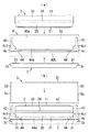
上記のように構成された液晶装置1を組み立てる際の手順等は適宜であるが、そのプロセスの一例を図7および図8に基づいて説明する。なお、図7は液晶装置1を側面側から見たもので、同図(a)は図2(a)のA−A線に沿う分解断面図、図7(b)は分解側面図である。また図8は液晶装置1を正面側から見たもので、同図(a)および(b)は図2(b)におけるC−C線に沿う断面図である。先ず、図7(a)および図8(a)に示すように液晶パネル2とバックライトユニット3とをフレーム4内に収容するもので、図の場合は液晶パネル2の対向基板20を下にして、該液晶パネル2を断面略H字形のフレーム4の上側の凹部40a内に挿入して嵌合保持させると共に、そのフレーム4の下側の凹部40b内にバックライトユニット3を挿入して嵌合保持させる構成である。その際、上記第1の可撓性基板29と第2の可撓性基板30は、図7に示すように、それぞれ液晶パネル2とバックライトユニット3から同方向(図の場合は左方)に引き出した状態でフレーム4の側壁部41に形成した切欠凹部41b,41cに係合させる。
The procedure for assembling the
次いで、図7(b)及び図8(b)のように上記フレーム4に嵌合保持させた液晶パネル2の外側(図の場合は上側)からカバー5を被せ、そのカバー5の対向面部52・52をフレーム4の側壁部43・43の外面に沿って下降移動させる。すると、図7(b)に示すカバー5の対向面部52・52に設けた舌状部52bの下端部が、図7(b)及び図8(b)に示す案内突起4cの傾斜面4c1に沿って外側方に押し開かれながら案内突起4c及び突起3cを乗り越えることによって、上記舌状部52bに設けた係止孔5cに突起3cが係合する。それによって上記カバー5がバックライトユニット3に連結される共に、そのカバー5とバックライトユニット3との間に液晶パネル2とフレーム4とが狭持された状態となり、それによって上記4つの部材2〜5が一体的に連結保持されるものである。
Next, as shown in FIGS. 7 (b) and 8 (b), the
上記のように本発明による液晶装置等の電気光学装置は、液晶パネル2等の電気光学パネルと、該電気光学パネルの背面に配設されるバックライトユニット3とを、フレーム4やカバー5などからなる実装ケースに保持させるようにした電気光学装置において、電気光学パネルに電気的に接続された第1の可撓性基板29と、バックライトユニット3に電気的に接続された第2の可撓性基板30とを備え、その第1と第2の可撓性基板29,30をそれぞれ実装ケースからそれぞれ同一方向に別々に引き出すようにしたから、例えば電気光学装置を組み立てたり製造する際には、上記第1及び第2の可撓性基板29,30をそれぞれ別々に引き出して別々に組付けることができる。
As described above, the electro-optical device such as the liquid crystal device according to the present invention includes the electro-optical panel such as the
また液晶パネル2やバックライトユニット3の検査や試験等を行う場合には、上記各可撓性基板29,30にテスターや検査機器を接続することによって、液晶パネル2やバックライトユニット3のそれぞれの電気的な故障や欠陥等を容易に発見することができる。またリワークやリペアを行う際には、第1の可撓性基板29と第2の可撓性基板30とが別々に設けられているので、従来のように分離する必要がなく、また無理に分離して配線が剥離する等の問題がないから極めて容易にリワークやリペアを行うことができる。
When the
なお、上記第1及び第2の可撓性基板29,30の実装ケースからの引き出し位置は適宜であるが、前述のように実装ケースの一側面から引き出すようにするとよく、本実施形態においては実装ケースとしてのフレーム4の一側面、図の場合はフレーム4の側壁部41に形成した切欠凹部41b,41cから前方に引き出すようにしたものである。このように構成すると、製造時の可撓性基板の引き出し作業や検査や試験および電子機器への接続や組付け作業を実装ケースの一側面側のみで容易に行うことができる。
The first and second
また上記実装ケースの構成も適宜であるが、前述のように電気光学パネルとバックライトユニットとを互いに対向配置させた状態で支持するためのフレーム、特に方形枠状のフレームを備えるとよく、本実施形態においては前述のように方形枠状のフレーム4に、電気光学パネルとしての液晶パネル2とバックライトユニット3とを互いに対向配置させた状態で嵌合保持させるようにしたものである。このように構成すると、液晶パネル2とバックライトユニット3とを互いに対向配置させた状態で簡単・確実に支持させることができると共に、フレーム4は方形枠状であるから、その中央部の開口部44aを介してバックライトユニット3からの光を液晶パネル2に良好に照射することができる。
The configuration of the mounting case is also appropriate, but as described above, a frame for supporting the electro-optical panel and the backlight unit in a state of being opposed to each other, particularly a rectangular frame-like frame, may be provided. In the embodiment, as described above, the
また上記第1及び第2の可撓性基板29,30の実装ケースからの引き出し長さは、前述のように、そのいずれか一方が他方よりも長く形成されているのが望ましい。上記実施形態においては、液晶パネル2に接続した第1の可撓性基板29のフレーム4からの引き出し長さが、バックライトユニット3に接続した第2の可撓性基板30の引き出し長さよりも長くなるようにしたものであるが、上記第2の可撓性基板30の引き出し長さの方が第1の可撓性基板29よりも長くなるようにしてもよい。このようにいずれか一方の引き出し長さが他方よりも長くなるようにすると、その各可撓性基板29,30を、外部の電源や制御回路等に接続する際に、それぞれ別々に容易に接続することができると共に、その接続時に互いに干渉したり、混線することがなく、容易・迅速に接続作業を行うことができる。
Further, as described above, it is desirable that one of the first and second
さらに上記第1及び第2の可撓性基板29,30の幅(図2(a)で上下方向の寸法)は、前述のように実装ケースの幅よりも狭く形成されているのが望ましい。上記実施形態においては、第1の可撓性基板29の幅は、実装ケースとしてのフレーム4の幅(図2(a)における上下方向の寸法)よりも狭く形成され、第2の可撓性基板30の幅(同上)はフレーム4および第1の可撓性基板29の幅よりもかなり狭く形成されている。上記のように第1及び第2の可撓性基板29,30の幅を、フレーム4等の実装ケースの幅よりも狭く形成すると、液晶装置等の電気光学装置の製造時または検査時にトレー等に載置する際、もしくは製品を梱包する際に、嵩張ることがなく、多数の電気光学装置を整然と載置または梱包することができる。また第1及び第2の可撓性基板29,30がフレーム4等の実装ケースよりも幅方向外方に飛び出して他物と接触したり、それによって他物や可撓性基板上の配線が損傷もしくは断線するのを未然に防止することができるものである。
Furthermore, it is desirable that the width of the first and second
なお、上記実装ケースとしてのフレーム4から引き出された第1及び第2の可撓性基板29,30は、その厚さ方向(図2(b)で上下方向)において互いに重なるように配置するとよく、図の実施形態は、図1に示すように第1の可撓性基板29の幅方向一端側の縁部の下方の重なる位置に第2の可撓性基板30を配置した構成であるが、第1の可撓性基板29に対する第2の可撓性基板30の配置位置は適宜である。上記のように第1と第2の可撓性基板29,30が厚さ方向に互いに重なるように配置すると、上記可撓性基板29,30が幅方向に張り出しで嵩張ったり他物と接触するのを更に低減することが可能となる。
The first and second
以上の実施形態は一例であり、例えば上記のようなフレーム4とカバー5とからなる実装ケースに限らず、その他各種の実装ケースにも適用することができる。また上記実施形態は、電気光学装置として液晶装置に適用し、電気光学パネルとしてアクティブマトリックス型の液晶パネルを用いた場合を例にして説明したが、パッシブマトリクス型の液晶パネルを用いてもよく、また液晶パネルに限らず、その他各種の電気光学パネルを用いて上記液晶装置と同様の構成の電気光学装置を得ることもできる。
The above embodiment is an example, and can be applied not only to the mounting case including the
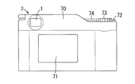
さらに上記のように構成した電気光学装置を各種の電気機器の表示部や表示装置等として用いることができる。図9はその一例を示すもので、上記のように構成された電気光学装置として液晶装置1を、電子機器7としてのデジタルカメラ70におけるエレクトリカルビューファインダ(EVF)として用いたものである。図中71は画像表示モニタ、72はシャッタボタン、73はダイヤルスイッチ、74は電源ボタンである。
Furthermore, the electro-optical device configured as described above can be used as a display unit, a display device, or the like of various electric apparatuses. FIG. 9 shows an example thereof, in which the
上記のように電気光学装置としての液晶装置1を、電子機器7としてのデジタルカメラ70におけるエレクトリカルビューファインダ(EVF)として用いた場合、電気光学パネルとして液晶パネル2に電気的に接続された第1の可撓性基板29と、その液晶パネル2に光を照射するためのバックライトユニット3に電気的に接続された第2の可撓性基板30とを上記フレーム4等の実装ケースからそれぞれ同一方向に別々に引き出したから、それらの可撓性基板29,30をデジタルカメラ70内の電源や信号入力源などに容易に接続することができる。また、その際の接続状況や液晶パネル2およびバックライトユニット3の動作状態その他各種の検査や試験を良好に行うことができると共に、リワークやリペアも容易に行うことができるものである。
As described above, when the
また本発明による電気光学装置は、上記のようなデジタルカメラに限らず、その他各種の電気機器にも適用可能であり、例えば携帯電話機やPDA(Personal Digital Assistants)と呼ばれる携帯型情報機器、携帯型パーソナルコンピュータ、パーソナルコンピュータ、ワークステーション、デジタルスチルカメラ、車載用モニタ、デジタルビデオカメラ、液晶テレビ、ビューファインダ型、モニタ直視型のビデオテープレコーダ、カーナビゲーション装置、ページャ、電子手帳、電卓、ワードプロセッサ、ワークステーション、テレビ電話機、及びPOS端末機などの電子機器にも広く利用することができる。上記いずれの場合にも上記と同様の作用効果が得られる。 The electro-optical device according to the present invention can be applied not only to the digital camera as described above but also to various other electric devices. For example, a portable information device called a mobile phone or a PDA (Personal Digital Assistants), a portable type Personal computer, personal computer, workstation, digital still camera, in-vehicle monitor, digital video camera, LCD TV, viewfinder type, monitor direct view type video tape recorder, car navigation device, pager, electronic notebook, calculator, word processor, work It can also be widely used in electronic devices such as stations, video phones, and POS terminals. In any of the above cases, the same effect as described above can be obtained.
1…液晶装置(電気光学装置)、2…液晶パネル(電気光学パネル)、3…バックライトユニット、3c…突起、4…フレーム、4a…パネル側部分、4b…バックライト側部分、4c…突起、5…カバー、5a…表示窓、5c…係止孔、7…電子機器、10…素子基板、20…対向基板、11、21…偏光板、12…画素電極、22…対向電極、13、23…配向膜、24…シール材、25…液晶層、29…第1の可撓性基板、30…第2の可撓性基板、31…両面接着テープ、40a,40b…凹部、41〜43…側壁部、41a、42a…突出部、43a…張り出し部、44…支持部、44a…開口部、51…平面部、52…対向面部、61、62…被覆層、70…デジタルカメラ。
DESCRIPTION OF
Claims (6)
前記電気光学パネルに電気的に接続された第1の可撓性基板と、前記バックライトユニットに電気的に接続された第2の可撓性基板とを備え、
前記実装ケースは、前記電気光学パネル及び前記バックライトユニットを収容するフレームと、前記電気光学パネルの一方の面を覆い前記バックライトユニットと係合されるカバーと、を含み、
前記フレームは、前記電気光学パネル及び前記バックライトユニットの側方に設けられた第1の側壁及び前記第1の側壁に対向するように配置された第2の側壁を有し、前記第1の側壁は、前記電気光学パネルの側方に形成された第1切欠部と、前記バックライトユニットの側方に形成された第2切欠部とを有し、
前記第1の可撓性基板は、前記第1の側壁に形成された第1切欠部から引き出されており、前記第2の可撓性基板は、前記第1の側壁に形成された第2切欠部から前記第1の可撓性基板と同一方向に引き出され、
前記カバーは、前記第1の側壁と前記第2の側壁との間に収まるように配置されることを特徴とする電気光学装置。 An electro-optical device in which an electro-optical panel and a backlight unit arranged to face the electro-optical panel are accommodated in a mounting case,
A first flexible substrate electrically connected to the electro-optical panel; and a second flexible substrate electrically connected to the backlight unit;
The mounting case includes a frame that houses the electro-optical panel and the backlight unit, and a cover that covers one surface of the electro-optical panel and is engaged with the backlight unit.
The frame has the electro-optical panel and a first sidewall and a second sidewall that is disposed so as to face the first side wall provided on a side of the backlight unit, the first The side wall has a first cutout formed on the side of the electro-optic panel and a second cutout formed on the side of the backlight unit,
The first flexible substrate is pulled out from a first cutout formed in the first side wall, and the second flexible substrate is a second formed on the first side wall. Pulled out from the notch in the same direction as the first flexible substrate ,
The electro-optical device according to claim 1, wherein the cover is disposed so as to fit between the first side wall and the second side wall .
Priority Applications (1)
| Application Number | Priority Date | Filing Date | Title |
|---|---|---|---|
| JP2009029917A JP5487635B2 (en) | 2009-02-12 | 2009-02-12 | Electro-optical device and electronic apparatus |
Applications Claiming Priority (1)
| Application Number | Priority Date | Filing Date | Title |
|---|---|---|---|
| JP2009029917A JP5487635B2 (en) | 2009-02-12 | 2009-02-12 | Electro-optical device and electronic apparatus |
Related Child Applications (1)
| Application Number | Title | Priority Date | Filing Date |
|---|---|---|---|
| JP2013269348A Division JP5708783B2 (en) | 2013-12-26 | 2013-12-26 | Electro-optical device, electronic apparatus, and support member |
Publications (3)
| Publication Number | Publication Date |
|---|---|
| JP2010186035A JP2010186035A (en) | 2010-08-26 |
| JP2010186035A5 JP2010186035A5 (en) | 2012-02-16 |
| JP5487635B2 true JP5487635B2 (en) | 2014-05-07 |
Family
ID=42766726
Family Applications (1)
| Application Number | Title | Priority Date | Filing Date |
|---|---|---|---|
| JP2009029917A Expired - Fee Related JP5487635B2 (en) | 2009-02-12 | 2009-02-12 | Electro-optical device and electronic apparatus |
Country Status (1)
| Country | Link |
|---|---|
| JP (1) | JP5487635B2 (en) |
Family Cites Families (5)
| Publication number | Priority date | Publication date | Assignee | Title |
|---|---|---|---|---|
| JPH1164830A (en) * | 1997-08-21 | 1999-03-05 | Citizen Watch Co Ltd | Liquid crystal display device |
| JP3436240B2 (en) * | 1999-07-14 | 2003-08-11 | 日本電気株式会社 | Flat panel display |
| JP2007233251A (en) * | 2006-03-03 | 2007-09-13 | Mitsubishi Electric Corp | Display device |
| JP3129206U (en) * | 2006-11-27 | 2007-02-08 | 船井電機株式会社 | LCD module |
| JP5076669B2 (en) * | 2007-06-20 | 2012-11-21 | エプソンイメージングデバイス株式会社 | Electro-optical device, holding frame, and electronic apparatus |
-
2009
- 2009-02-12 JP JP2009029917A patent/JP5487635B2/en not_active Expired - Fee Related
Also Published As
| Publication number | Publication date |
|---|---|
| JP2010186035A (en) | 2010-08-26 |
Similar Documents
| Publication | Publication Date | Title |
|---|---|---|
| JP5386941B2 (en) | ELECTRO-OPTICAL DEVICE, MANUFACTURING METHOD THEREOF, AND ELECTRONIC DEVICE | |
| US8319109B2 (en) | Electro-optical device and electronic apparatus | |
| US7667798B2 (en) | Liquid crystal display device | |
| JP4244942B2 (en) | Liquid crystal device, lighting device, and electronic device | |
| JP5257010B2 (en) | Electro-optical device and electronic apparatus | |
| JP5262601B2 (en) | Electro-optical device and electronic apparatus | |
| JP5458549B2 (en) | Electro-optical device and electronic apparatus | |
| CN107664863B (en) | Liquid crystal display device | |
| JP2010096801A (en) | Electro-optic device and electronic equipment | |
| JP2004341216A (en) | ELECTRO-OPTICAL DEVICE SUBSTRATE AND MANUFACTURING METHOD THEREOF, ELECTRO-OPTICAL DEVICE AND ELECTRONIC EQUIPMENT HAVING THE ELECTRO-OPTICAL DEVICE SUBSTRATE | |
| JP2009020272A (en) | Electro-optical device and electronic equipment | |
| US9069199B2 (en) | Liquid crystal module and liquid crystal display device including the same | |
| JP5487635B2 (en) | Electro-optical device and electronic apparatus | |
| JP5708783B2 (en) | Electro-optical device, electronic apparatus, and support member | |
| JP7126844B2 (en) | Connected display device | |
| JP5458550B2 (en) | Electro-optical device and electronic apparatus | |
| JP5257011B2 (en) | Electro-optical device and electronic apparatus | |
| JP2010073389A (en) | Plane light source device and liquid crystal display | |
| JP5417808B2 (en) | Electro-optical device and electronic apparatus | |
| KR101777127B1 (en) | Flat panel display device and mathod for manufacturing the same | |
| KR20070056780A (en) | LCD Display | |
| JP2007192853A (en) | Fabricating method of electrooptical device | |
| JP2005326473A (en) | Electro-optical device manufacturing method, illumination device manufacturing method, electro-optical device, illumination device, and electronic apparatus | |
| JPH08278511A (en) | Device having circuit board and liquid crystal display device | |
| JP4857605B2 (en) | Electro-optical device, method of manufacturing electro-optical device, and electronic apparatus |
Legal Events
| Date | Code | Title | Description |
|---|---|---|---|
| A521 | Request for written amendment filed |
Free format text: JAPANESE INTERMEDIATE CODE: A523 Effective date: 20111221 |
|
| A621 | Written request for application examination |
Free format text: JAPANESE INTERMEDIATE CODE: A621 Effective date: 20111221 |
|
| A977 | Report on retrieval |
Free format text: JAPANESE INTERMEDIATE CODE: A971007 Effective date: 20121121 |
|
| A131 | Notification of reasons for refusal |
Free format text: JAPANESE INTERMEDIATE CODE: A131 Effective date: 20121127 |
|
| A02 | Decision of refusal |
Free format text: JAPANESE INTERMEDIATE CODE: A02 Effective date: 20131001 |
|
| A521 | Request for written amendment filed |
Free format text: JAPANESE INTERMEDIATE CODE: A523 Effective date: 20131226 |
|
| A911 | Transfer to examiner for re-examination before appeal (zenchi) |
Free format text: JAPANESE INTERMEDIATE CODE: A911 Effective date: 20140109 |
|
| TRDD | Decision of grant or rejection written | ||
| A01 | Written decision to grant a patent or to grant a registration (utility model) |
Free format text: JAPANESE INTERMEDIATE CODE: A01 Effective date: 20140128 |
|
| A61 | First payment of annual fees (during grant procedure) |
Free format text: JAPANESE INTERMEDIATE CODE: A61 Effective date: 20140210 |
|
| R150 | Certificate of patent or registration of utility model |
Ref document number: 5487635 Country of ref document: JP Free format text: JAPANESE INTERMEDIATE CODE: R150 |
|
| S531 | Written request for registration of change of domicile |
Free format text: JAPANESE INTERMEDIATE CODE: R313531 |
|
| R350 | Written notification of registration of transfer |
Free format text: JAPANESE INTERMEDIATE CODE: R350 |
|
| LAPS | Cancellation because of no payment of annual fees |