JP5439060B2 - 表示装置 - Google Patents
表示装置 Download PDFInfo
- Publication number
- JP5439060B2 JP5439060B2 JP2009155201A JP2009155201A JP5439060B2 JP 5439060 B2 JP5439060 B2 JP 5439060B2 JP 2009155201 A JP2009155201 A JP 2009155201A JP 2009155201 A JP2009155201 A JP 2009155201A JP 5439060 B2 JP5439060 B2 JP 5439060B2
- Authority
- JP
- Japan
- Prior art keywords
- pixel
- display
- signal
- pixel signal
- drive
- Prior art date
- Legal status (The legal status is an assumption and is not a legal conclusion. Google has not performed a legal analysis and makes no representation as to the accuracy of the status listed.)
- Expired - Fee Related
Links
Images


Classifications
-
- G—PHYSICS
- G06—COMPUTING; CALCULATING OR COUNTING
- G06F—ELECTRIC DIGITAL DATA PROCESSING
- G06F3/00—Input arrangements for transferring data to be processed into a form capable of being handled by the computer; Output arrangements for transferring data from processing unit to output unit, e.g. interface arrangements
- G06F3/01—Input arrangements or combined input and output arrangements for interaction between user and computer
- G06F3/03—Arrangements for converting the position or the displacement of a member into a coded form
- G06F3/041—Digitisers, e.g. for touch screens or touch pads, characterised by the transducing means
- G06F3/0416—Control or interface arrangements specially adapted for digitisers
- G06F3/04166—Details of scanning methods, e.g. sampling time, grouping of sub areas or time sharing with display driving
-
- G—PHYSICS
- G06—COMPUTING; CALCULATING OR COUNTING
- G06F—ELECTRIC DIGITAL DATA PROCESSING
- G06F3/00—Input arrangements for transferring data to be processed into a form capable of being handled by the computer; Output arrangements for transferring data from processing unit to output unit, e.g. interface arrangements
- G06F3/01—Input arrangements or combined input and output arrangements for interaction between user and computer
- G06F3/03—Arrangements for converting the position or the displacement of a member into a coded form
- G06F3/041—Digitisers, e.g. for touch screens or touch pads, characterised by the transducing means
- G06F3/0412—Digitisers structurally integrated in a display
-
- G—PHYSICS
- G06—COMPUTING; CALCULATING OR COUNTING
- G06F—ELECTRIC DIGITAL DATA PROCESSING
- G06F3/00—Input arrangements for transferring data to be processed into a form capable of being handled by the computer; Output arrangements for transferring data from processing unit to output unit, e.g. interface arrangements
- G06F3/01—Input arrangements or combined input and output arrangements for interaction between user and computer
- G06F3/03—Arrangements for converting the position or the displacement of a member into a coded form
- G06F3/041—Digitisers, e.g. for touch screens or touch pads, characterised by the transducing means
- G06F3/044—Digitisers, e.g. for touch screens or touch pads, characterised by the transducing means by capacitive means
- G06F3/0446—Digitisers, e.g. for touch screens or touch pads, characterised by the transducing means by capacitive means using a grid-like structure of electrodes in at least two directions, e.g. using row and column electrodes
-
- G—PHYSICS
- G06—COMPUTING; CALCULATING OR COUNTING
- G06F—ELECTRIC DIGITAL DATA PROCESSING
- G06F3/00—Input arrangements for transferring data to be processed into a form capable of being handled by the computer; Output arrangements for transferring data from processing unit to output unit, e.g. interface arrangements
- G06F3/01—Input arrangements or combined input and output arrangements for interaction between user and computer
- G06F3/03—Arrangements for converting the position or the displacement of a member into a coded form
- G06F3/041—Digitisers, e.g. for touch screens or touch pads, characterised by the transducing means
- G06F3/045—Digitisers, e.g. for touch screens or touch pads, characterised by the transducing means using resistive elements, e.g. a single continuous surface or two parallel surfaces put in contact
-
- G—PHYSICS
- G09—EDUCATION; CRYPTOGRAPHY; DISPLAY; ADVERTISING; SEALS
- G09G—ARRANGEMENTS OR CIRCUITS FOR CONTROL OF INDICATING DEVICES USING STATIC MEANS TO PRESENT VARIABLE INFORMATION
- G09G3/00—Control arrangements or circuits, of interest only in connection with visual indicators other than cathode-ray tubes
- G09G3/20—Control arrangements or circuits, of interest only in connection with visual indicators other than cathode-ray tubes for presentation of an assembly of a number of characters, e.g. a page, by composing the assembly by combination of individual elements arranged in a matrix no fixed position being assigned to or needed to be assigned to the individual characters or partial characters
- G09G3/34—Control arrangements or circuits, of interest only in connection with visual indicators other than cathode-ray tubes for presentation of an assembly of a number of characters, e.g. a page, by composing the assembly by combination of individual elements arranged in a matrix no fixed position being assigned to or needed to be assigned to the individual characters or partial characters by control of light from an independent source
- G09G3/36—Control arrangements or circuits, of interest only in connection with visual indicators other than cathode-ray tubes for presentation of an assembly of a number of characters, e.g. a page, by composing the assembly by combination of individual elements arranged in a matrix no fixed position being assigned to or needed to be assigned to the individual characters or partial characters by control of light from an independent source using liquid crystals
- G09G3/3607—Control arrangements or circuits, of interest only in connection with visual indicators other than cathode-ray tubes for presentation of an assembly of a number of characters, e.g. a page, by composing the assembly by combination of individual elements arranged in a matrix no fixed position being assigned to or needed to be assigned to the individual characters or partial characters by control of light from an independent source using liquid crystals for displaying colours or for displaying grey scales with a specific pixel layout, e.g. using sub-pixels
-
- G—PHYSICS
- G09—EDUCATION; CRYPTOGRAPHY; DISPLAY; ADVERTISING; SEALS
- G09G—ARRANGEMENTS OR CIRCUITS FOR CONTROL OF INDICATING DEVICES USING STATIC MEANS TO PRESENT VARIABLE INFORMATION
- G09G3/00—Control arrangements or circuits, of interest only in connection with visual indicators other than cathode-ray tubes
- G09G3/20—Control arrangements or circuits, of interest only in connection with visual indicators other than cathode-ray tubes for presentation of an assembly of a number of characters, e.g. a page, by composing the assembly by combination of individual elements arranged in a matrix no fixed position being assigned to or needed to be assigned to the individual characters or partial characters
- G09G3/34—Control arrangements or circuits, of interest only in connection with visual indicators other than cathode-ray tubes for presentation of an assembly of a number of characters, e.g. a page, by composing the assembly by combination of individual elements arranged in a matrix no fixed position being assigned to or needed to be assigned to the individual characters or partial characters by control of light from an independent source
- G09G3/36—Control arrangements or circuits, of interest only in connection with visual indicators other than cathode-ray tubes for presentation of an assembly of a number of characters, e.g. a page, by composing the assembly by combination of individual elements arranged in a matrix no fixed position being assigned to or needed to be assigned to the individual characters or partial characters by control of light from an independent source using liquid crystals
- G09G3/3611—Control of matrices with row and column drivers
- G09G3/3614—Control of polarity reversal in general
-
- G—PHYSICS
- G09—EDUCATION; CRYPTOGRAPHY; DISPLAY; ADVERTISING; SEALS
- G09G—ARRANGEMENTS OR CIRCUITS FOR CONTROL OF INDICATING DEVICES USING STATIC MEANS TO PRESENT VARIABLE INFORMATION
- G09G3/00—Control arrangements or circuits, of interest only in connection with visual indicators other than cathode-ray tubes
- G09G3/20—Control arrangements or circuits, of interest only in connection with visual indicators other than cathode-ray tubes for presentation of an assembly of a number of characters, e.g. a page, by composing the assembly by combination of individual elements arranged in a matrix no fixed position being assigned to or needed to be assigned to the individual characters or partial characters
- G09G3/34—Control arrangements or circuits, of interest only in connection with visual indicators other than cathode-ray tubes for presentation of an assembly of a number of characters, e.g. a page, by composing the assembly by combination of individual elements arranged in a matrix no fixed position being assigned to or needed to be assigned to the individual characters or partial characters by control of light from an independent source
- G09G3/36—Control arrangements or circuits, of interest only in connection with visual indicators other than cathode-ray tubes for presentation of an assembly of a number of characters, e.g. a page, by composing the assembly by combination of individual elements arranged in a matrix no fixed position being assigned to or needed to be assigned to the individual characters or partial characters by control of light from an independent source using liquid crystals
- G09G3/3611—Control of matrices with row and column drivers
- G09G3/3648—Control of matrices with row and column drivers using an active matrix
- G09G3/3655—Details of drivers for counter electrodes, e.g. common electrodes for pixel capacitors or supplementary storage capacitors
-
- G—PHYSICS
- G09—EDUCATION; CRYPTOGRAPHY; DISPLAY; ADVERTISING; SEALS
- G09G—ARRANGEMENTS OR CIRCUITS FOR CONTROL OF INDICATING DEVICES USING STATIC MEANS TO PRESENT VARIABLE INFORMATION
- G09G3/00—Control arrangements or circuits, of interest only in connection with visual indicators other than cathode-ray tubes
- G09G3/20—Control arrangements or circuits, of interest only in connection with visual indicators other than cathode-ray tubes for presentation of an assembly of a number of characters, e.g. a page, by composing the assembly by combination of individual elements arranged in a matrix no fixed position being assigned to or needed to be assigned to the individual characters or partial characters
- G09G3/34—Control arrangements or circuits, of interest only in connection with visual indicators other than cathode-ray tubes for presentation of an assembly of a number of characters, e.g. a page, by composing the assembly by combination of individual elements arranged in a matrix no fixed position being assigned to or needed to be assigned to the individual characters or partial characters by control of light from an independent source
- G09G3/36—Control arrangements or circuits, of interest only in connection with visual indicators other than cathode-ray tubes for presentation of an assembly of a number of characters, e.g. a page, by composing the assembly by combination of individual elements arranged in a matrix no fixed position being assigned to or needed to be assigned to the individual characters or partial characters by control of light from an independent source using liquid crystals
- G09G3/3611—Control of matrices with row and column drivers
- G09G3/3648—Control of matrices with row and column drivers using an active matrix
- G09G3/3659—Control of matrices with row and column drivers using an active matrix the addressing of the pixel involving the control of two or more scan electrodes or two or more data electrodes, e.g. pixel voltage dependant on signal of two data electrodes
-
- G—PHYSICS
- G09—EDUCATION; CRYPTOGRAPHY; DISPLAY; ADVERTISING; SEALS
- G09G—ARRANGEMENTS OR CIRCUITS FOR CONTROL OF INDICATING DEVICES USING STATIC MEANS TO PRESENT VARIABLE INFORMATION
- G09G3/00—Control arrangements or circuits, of interest only in connection with visual indicators other than cathode-ray tubes
- G09G3/20—Control arrangements or circuits, of interest only in connection with visual indicators other than cathode-ray tubes for presentation of an assembly of a number of characters, e.g. a page, by composing the assembly by combination of individual elements arranged in a matrix no fixed position being assigned to or needed to be assigned to the individual characters or partial characters
- G09G3/34—Control arrangements or circuits, of interest only in connection with visual indicators other than cathode-ray tubes for presentation of an assembly of a number of characters, e.g. a page, by composing the assembly by combination of individual elements arranged in a matrix no fixed position being assigned to or needed to be assigned to the individual characters or partial characters by control of light from an independent source
- G09G3/36—Control arrangements or circuits, of interest only in connection with visual indicators other than cathode-ray tubes for presentation of an assembly of a number of characters, e.g. a page, by composing the assembly by combination of individual elements arranged in a matrix no fixed position being assigned to or needed to be assigned to the individual characters or partial characters by control of light from an independent source using liquid crystals
- G09G3/3611—Control of matrices with row and column drivers
- G09G3/3696—Generation of voltages supplied to electrode drivers
-
- G—PHYSICS
- G06—COMPUTING; CALCULATING OR COUNTING
- G06F—ELECTRIC DIGITAL DATA PROCESSING
- G06F2203/00—Indexing scheme relating to G06F3/00 - G06F3/048
- G06F2203/041—Indexing scheme relating to G06F3/041 - G06F3/045
- G06F2203/04101—2.5D-digitiser, i.e. digitiser detecting the X/Y position of the input means, finger or stylus, also when it does not touch, but is proximate to the digitiser's interaction surface and also measures the distance of the input means within a short range in the Z direction, possibly with a separate measurement setup
-
- G—PHYSICS
- G06—COMPUTING; CALCULATING OR COUNTING
- G06F—ELECTRIC DIGITAL DATA PROCESSING
- G06F2203/00—Indexing scheme relating to G06F3/00 - G06F3/048
- G06F2203/041—Indexing scheme relating to G06F3/041 - G06F3/045
- G06F2203/04112—Electrode mesh in capacitive digitiser: electrode for touch sensing is formed of a mesh of very fine, normally metallic, interconnected lines that are almost invisible to see. This provides a quite large but transparent electrode surface, without need for ITO or similar transparent conductive material
-
- G—PHYSICS
- G06—COMPUTING; CALCULATING OR COUNTING
- G06F—ELECTRIC DIGITAL DATA PROCESSING
- G06F2218/00—Aspects of pattern recognition specially adapted for signal processing
- G06F2218/02—Preprocessing
- G06F2218/04—Denoising
-
- G—PHYSICS
- G09—EDUCATION; CRYPTOGRAPHY; DISPLAY; ADVERTISING; SEALS
- G09G—ARRANGEMENTS OR CIRCUITS FOR CONTROL OF INDICATING DEVICES USING STATIC MEANS TO PRESENT VARIABLE INFORMATION
- G09G2310/00—Command of the display device
- G09G2310/02—Addressing, scanning or driving the display screen or processing steps related thereto
- G09G2310/0243—Details of the generation of driving signals
- G09G2310/0248—Precharge or discharge of column electrodes before or after applying exact column voltages
-
- G—PHYSICS
- G09—EDUCATION; CRYPTOGRAPHY; DISPLAY; ADVERTISING; SEALS
- G09G—ARRANGEMENTS OR CIRCUITS FOR CONTROL OF INDICATING DEVICES USING STATIC MEANS TO PRESENT VARIABLE INFORMATION
- G09G2310/00—Command of the display device
- G09G2310/02—Addressing, scanning or driving the display screen or processing steps related thereto
- G09G2310/0243—Details of the generation of driving signals
- G09G2310/0251—Precharge or discharge of pixel before applying new pixel voltage
-
- G—PHYSICS
- G09—EDUCATION; CRYPTOGRAPHY; DISPLAY; ADVERTISING; SEALS
- G09G—ARRANGEMENTS OR CIRCUITS FOR CONTROL OF INDICATING DEVICES USING STATIC MEANS TO PRESENT VARIABLE INFORMATION
- G09G2310/00—Command of the display device
- G09G2310/02—Addressing, scanning or driving the display screen or processing steps related thereto
- G09G2310/0262—The addressing of the pixel, in a display other than an active matrix LCD, involving the control of two or more scan electrodes or two or more data electrodes, e.g. pixel voltage dependent on signals of two data electrodes
-
- G—PHYSICS
- G09—EDUCATION; CRYPTOGRAPHY; DISPLAY; ADVERTISING; SEALS
- G09G—ARRANGEMENTS OR CIRCUITS FOR CONTROL OF INDICATING DEVICES USING STATIC MEANS TO PRESENT VARIABLE INFORMATION
- G09G2320/00—Control of display operating conditions
- G09G2320/02—Improving the quality of display appearance
- G09G2320/0204—Compensation of DC component across the pixels in flat panels
-
- G—PHYSICS
- G09—EDUCATION; CRYPTOGRAPHY; DISPLAY; ADVERTISING; SEALS
- G09G—ARRANGEMENTS OR CIRCUITS FOR CONTROL OF INDICATING DEVICES USING STATIC MEANS TO PRESENT VARIABLE INFORMATION
- G09G2320/00—Control of display operating conditions
- G09G2320/02—Improving the quality of display appearance
- G09G2320/0209—Crosstalk reduction, i.e. to reduce direct or indirect influences of signals directed to a certain pixel of the displayed image on other pixels of said image, inclusive of influences affecting pixels in different frames or fields or sub-images which constitute a same image, e.g. left and right images of a stereoscopic display
-
- G—PHYSICS
- G09—EDUCATION; CRYPTOGRAPHY; DISPLAY; ADVERTISING; SEALS
- G09G—ARRANGEMENTS OR CIRCUITS FOR CONTROL OF INDICATING DEVICES USING STATIC MEANS TO PRESENT VARIABLE INFORMATION
- G09G2320/00—Control of display operating conditions
- G09G2320/02—Improving the quality of display appearance
- G09G2320/0219—Reducing feedthrough effects in active matrix panels, i.e. voltage changes on the scan electrode influencing the pixel voltage due to capacitive coupling
-
- G—PHYSICS
- G09—EDUCATION; CRYPTOGRAPHY; DISPLAY; ADVERTISING; SEALS
- G09G—ARRANGEMENTS OR CIRCUITS FOR CONTROL OF INDICATING DEVICES USING STATIC MEANS TO PRESENT VARIABLE INFORMATION
- G09G2320/00—Control of display operating conditions
- G09G2320/02—Improving the quality of display appearance
- G09G2320/029—Improving the quality of display appearance by monitoring one or more pixels in the display panel, e.g. by monitoring a fixed reference pixel
Description
しかしながら、タッチパネルを液晶パネルに設けると、液晶モジュールの全体の厚さが厚くなる。そこで、例えば特許文献1には、薄型化に適した構造の、静電容量型タッチパネル付き液晶表示素子が提案されている。
表示駆動のための信号線や電極は、表示のために画素信号が印加され、あるいは、例えば液晶層等の表示機能層に付与する表示電圧の電位基準(表示基準電位)を交流反転することで駆動される場合がある。そのため、これらの表示のための電位変動が駆動電極を介して検出電極の電位を揺らし、これが物体検出にとってノイズ源となることがある。
以下、次の順で説明を行う。
1.第1の実施の形態:1H期間内に異なる極性の画素信号を含む実施の形態であり、特に好ましい形態として、交互に極性反転する場合を例示するものである。
2.第2の実施の形態:1画素内の2領域(もしくは画素ペアとなる2画素)の同一画素信号による駆動例を示す実施の形態である。
3.変形例
[表示装置の基本構成]
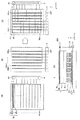
図1(A)〜図1(C)に、本実施の形態に関わる表示装置の電極と、その駆動や検出のための回路の配置に特化した平面図を示す。また、図1(D)に、本実施形態に関わる表示装置の概略的な断面構造を示す。図1(D)は、例えば行方向(画素表示ライン方向)の6画素分の断面を表している。図2は、画素の等価回路図である。
図1に図解する表示装置は、「表示機能層」としての液晶層を備える液晶表示装置である。
図1(D)では断面構造を見易くするために、この本発明の主要な構成である、駆動電極、画素電極および検出電極についてはハッチングを付すが、それ以外の部分(基板、絶縁膜および機能膜等)についてはハッチングを省略している。このハッチングの省略は、これ以降の他の断面構造図においても同様である。
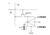
TFT23のゲートは行方向、即ち表示画面の横方向に並ぶ全ての画素PIXで電気的に共通化され、これにより表示走査線が形成されている。この表示走査線は、不図示の垂直駆動回路から出力され、TFT23のゲートを開閉するためのゲートパルスが供給されるため、以下、ゲート線GLと称する。
駆動電極43は、タッチ検出動作を行うタッチセンサの一部を構成するタッチ検出センサの駆動電極DEとしても兼用されるものである。
各駆動電極は、x方向に長い帯状に形成され、y方向に同一ピッチでkm個配置されている。このうちk個の駆動電極43で、同時駆動される駆動電極群DEj(j=1,2,3,…,m)の各々が構成される。各駆動電極43は、n本のセンサ線SNL1〜SNLnと異なる方向に配置されている。本例では、駆動電極DEjとセンサ線SNLiが直交して配置されている。
なお、接触検出部8は液晶表示装置1の外部に配置されていてもよいが、本例では液晶表示装置1が接触検出部8を内蔵している。
ここで“検出走査駆動”とは、検出駆動電圧(例えば交流電圧)を印加する動作と、その印加対象を一方向(第1方向、ここではy方向)内でシフトするシフト動作とを行う動作である。例えば一定の共通電位Vcomが印加されている駆動電極43(単数でもよいが、ここでは隣接するk本の駆動電極43)に、検出駆動電圧(ACパルス信号)が印加される。検出駆動電圧が印加される駆動電極以外の駆動電極は一定の共通電位Vcomで保持される。
つまり、表示走査の画素ラインでは、図2のゲート線GLの活性化によりTFT23がオンしてソース線SLの画素信号が画素電極22に書き込まれる。そのとき駆動電極43は一定の共通電位Vcomで保持する必要から、タッチ検出走査のための検出駆動電圧を駆動電極43に印加できない。
この構成によって、接触検出部8は、どの検出回路DETに電圧変化が生じたかで行方向の位置が検出でき、その検出時のタイミングによって列方向の位置情報を得ることができる。つまり、駆動制御部9の検出駆動電圧の走査と接触検出部8の動作が、例えば所定周期のクロック信号で同期しているとする。このような同期動作によって、接触検出部8が電圧変化を得たときが、駆動制御部9が、どの駆動電極を駆動していたときに対応するかが分かるため、指の接触位置中心を検出できる。このような検出動作は、液晶表示装置1全体を統括する不図示のコンピュータベースの統括制御回路、例えばCPUやマイクロコンピュータ、あるいは、タッチ検出のための制御回路により制御される。
TFTが多く集積化されているため製造工程数を減らすには駆動基板2に接触検出部8も一緒に形成することが望ましい。ただし、センサ線SNLが対向基板4側に存在し、センサ線SNLが透明電極材料から形成されるため配線抵抗が高くなることがある。そのような場合、配線抵抗が高いことの不具合を回避するには、対向基板4側に接触検出部8を形成することが好ましい。ただし、接触検出部8だけのために対向基板4にTFT形成プロセスを用いると、コスト高になるという不利益がある。以上の利益と不利益を総合的に勘案して、接触検出部8の形成位置を決定するとよい。
図3に、FFS(Field Fringe Switching)方式の液晶の画素(PIX)におけるTFT基板21の上面視を示す。
画素電極22は、コンタクト46を介して下層のアルミニウム(AL)等からなる内部配線47と接続されている。内部配線47が、ポリシリコン(PS)からなるTFT23の薄膜半導体層48に形成されたソースとドレインの一方に接続されている。薄膜半導体層48のソースとドレインの他方に、アルミニウム(AL)からなるソース線SLが接続されている。薄膜半導体層48の下層に交差するゲート線GLが、モリブデン(Mo)等のゲートメタル(GM)から形成され、ソース線SLと直交する向きに配置されている。
図4は、画素ごとに画素信号の極性を反転するドット反転が可能なドライバ構成例を示すブロック図である。
図4に図解する液晶表示装置1は、図2および図3に示す画素PIXがマトリクス配置された表示部100を有する。
表示部100からは、s本のソース線SL1〜SLsがy方向の一方から引き出され、km本のゲート線GL1〜GLkmがx方向の一方から引き出されている。
また、ソースドライバ300とゲートドライバ400には、これらを制御する表示制御回路(DIS_CONT)200が接続されている。
例えば、これらソースドライバ300、ゲートドライバ400および表示制御回路200により、本発明の“画素信号制御部”の実施例を構成する。
また、表示制御回路200は、データスタートパルス信号SSPと、データクロック信号SCKと、短絡制御信号Cshとを発生し、これらをソースドライバ300に与える。
データクロック信号SCKは、水平同期信号HSYに基づき1水平走査期間(1H)ごとに所定期間だけハイレベル(Hレベル)となる信号であり、ソースドライバ300の1Hシフト動作の開始と終了を制御する信号である。この動作によりデジタル画素信号DAが所定数(例えば、4、6、12等)の出力選択経路に分配される。例えば6セレクタ方式の場合、6本のソース線SLごとに所定数(s/6)の画素信号が同時に出力され、この動作が全部で6回繰り返されて1H期間の画素信号排出が行われる。
短絡制御信号Cshは、ドット反転時に用いられる信号であり、水平同期信号HSYおよび制御信号Dcに基づき表示制御回路200で発生し、ソースドライバ300に与えられる。
ゲートスタートパルス信号GSPは、垂直同期信号VSYに基づき1フレーム期間(1垂直走査期間)のうち所定期間にHレベルとなる信号である。
ゲートドライバ出力イネーブル信号GOEは、水平同期信号HSYおよび制御信号Dcに基づき発生する。このゲートドライバ出力イネーブル信号GOEとゲートスタートパルス信号GSPによって、ゲートドライバ400が、1フレーム(1F)表示動作の開始と終了を制御する。
局部的な液晶のDCバイアスを平均化する意味で、画素ごとに1H周期で画素信号の極性が反転することが望ましい。
本実施の形態では、1H期間ごとの共通電位Vcomの反転は、基本的には行わないが、その理由について説明する。
図5に図解する配色の例では、画素列ごとに赤(R),緑(G),青(B)の1色が配置されている。例えばソース線SL1とSL4に赤(R)の画素信号であるR1信号とR2信号が異なるタイミングで与えられる。ソース線SL2とSL5に緑(G)の画素信号であるG1信号とG2信号が異なるタイミング与えられる。また、ソース線SL3とSL6に青(B)の画素信号であるB1信号とB2信号が異なるタイミングで与えられる。
G1信号はソース線SL2を含む第2番目、第8番目、…のソース線ソース線に同時に与えられ、G2信号はソース線SL5を含む第5番目、第11番目、…のソース線に同時に与えられる。
同様に、B1信号はソース線SL3を含む第3番目、第9番目、…のソース線2同時に与えられ、B2信号はソース線SL6を含む第6番目、第12番目、…のソース線に同時に与えられる。
1HVcom反転駆動を行う比較例の場合、1水平期間(1H)ごとに対向電極(駆動電極43)の電位である共通電位Vcomが、例えば0Vを中心に反転駆動される。
共通電位Vcomが正極のときは画素信号が負パルス、逆に、共通電位Vcomが負極の時は画素信号が正パルスとして与えられる。液晶層6は電界の向きが逆でも同じ電圧値が与えられると同一階調の表示となる。なお、図6では、1H期間ごとの6つのパルスを、図5の色信号の符号により表している。
検出電位が全体的に減衰しているのはセンサ線SNL自身の配線抵抗、ならびに、検出回路が抵抗を有するためである。その減衰の1H期間終了までの到達点、つまり共通電位Vcomが正極から負極に変化する直前での階調差によって電位差ΔVが生じていることがわかる。この電位差は次の負極の共通電位Vcomにおいて、初期電位差として継承されている。物体検出は、この極性変化後にセンサ線出力の波高値が減衰する前の高いレベルにおいて、被検出物の接近で変化する(より低下する)ことを検出するため、この電位差ΔVは、そのまま物体検出の誤差成分となる。
図8(A)は、この誤差の極性を模式的に示す図である。
前述したように駆動電極43(図1参照)は、ソース線SL1〜SLkmの各々と交差して配置されるため、両者は多少なりとも容量結合している。この容量結合の強さは表示装置を薄型化すればするだけ増大する。従って図8(A)に示す結合容量C1〜C6は、ソース線SL1〜SL6の各々が駆動電極(対向電極)43と電気的に結合する強さを表している。
一方、駆動電極43は、それと直交するセンサ線SNLと静電容量Csで電気的に結合している。従って、ソース線SL1〜SLkmの電位が画素信号パルスの印加で変化すると、それが更に、駆動電極43から静電容量を介してセンサ線SNLに伝達される。
以上の不具合を防止するため、本実施の形態では以下の対策を行っている。
図9に、本実施の形態における共通電位Vcomと画素信号とを示す。
本実施の形態では、1H表示期間中は、共通電位Vcomは一定電位とする。この要件を満たす場合としては、1H表示期間が次の1H表示期間に推移しても、検出駆動がなされない限り共通電位Vcomは一定電位とする場合がある。さらに、共通電位Vcomを1Hごとに反転駆動する場合も、この要件を満たす。つまり、共通電位Vcomは一定電位とするのは、「少なくとも1H期間中は」であり、それ以外は任意である。
図7の例でも分かるように、負極性の白表示(W)が「+」の誤差要因となるため、画素信号の極性と反対の極性が潜在的な誤差要因となる。よって、図9(B)のパルス極性制御では、第1番目の画素ラインにおいては、潜在的な誤差要因の極性が「+」,「−」,「+」,…の順で存在する。
上記第1の実施の形態では、ノイズ成分の発生がなくなる前提としては、正極性のパルスと負極正のパルスが波高値において均衡している場合が挙げられる。このような場合としてはある特定色が水平画素行の全域で表示されている場合などであるが、表示内容によってはノイズ発生効果が変動することが予想される。
本実施の形態では、第1の実施の形態と同様、表示制御時に共通電位Vcomは一定電位とする。また、1H期間内における、極性反転のパルス数は、極性反転していないパルス数と等しいという、より望ましい観点も満たしている。
このとき画素ラインの1つの画素が図6に示す通常の1画素構成ならば、極性が異なる画素信号同士が相殺してしまう。
なお、本発明で“同時”というとき、実質的に同時期に制御を行う意味であり、僅かな時間差は許容される。
第1の方法では、図12の列方向(y方向)の2領域(または2画素)を1画素のように駆動する場合、異なる極性の画素信号を2領域(または2画素)で取り込む必要がある。この場合、画素信号には正極性パルスと負極性パルスが交互に印加されており、そのパルスのサンプリングタイミングを、表示制御回路200およびゲートドライバ400によるTFT23のターンオンのタイミングで制御する。
この場合、画素信号そのものの電位変動が平均化され、ノイズ発生が発生源で抑圧されている。
これにより個々の画素信号線の電位変動は抑制できないが、駆動電極43で、その電位変動を相殺してセンサ検出精度への影響を予め排除できる。
図9では、R1信号、R2信号、G1信号、G2信号、B1信号、B2信号の各々は、それぞれ(s/6)本の画素信号線(ソース線SL)に同一極性の画素信号パルスとして供給される。セレクタ方式を変更して、例えばR1信号とR2信号の各半分が同時供給され、残りの各半分が同時供給されるようにして、時間的に駆動電極43に重畳するノイズを相殺することができる。この場合、各ソース線SLでの電位変動は抑制されないが、異なる極性のノイズなので駆動電極43で相殺される。結果として、センサ線SNLへのノイズ重畳は防止または抑止される。
例えば、操作画面を表示し、指等によるタッチ検出による操作が予想される場合は、画素分割モードにしてセンサ検出精度を高め、その他の映像再生時等には画素分割モードを解除して高品質な映像表示を行うようにしてよい。
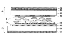
前述したように、横電界モードでは、画素電極22と駆動電極43が駆動基板2側に配置される。
TFT基板21は、その画素電極22側を液晶層6に隣接させ、ガラス基板41と貼り合わされている。液晶層6は不図示のスペーサで強度的に保たれている。
一方、TFT基板21の背面には第1偏光板61が貼られ、これと偏光の向きが異なる第2偏光板62が、基材49の表示面側に貼られている。
第2偏光板62の表示面側に不図示の保護層が形成される。
図14に示す構造では、センサ線SNLが基材49に予め形成されて、例えばロール状の部材として貼られるが、図15ではガラス基板41の表示面側にセンサ線SNLを形成し、その上に第2偏光板62が貼られる。
とくに極性が反転した画素が隣接していると、タッチ検出精度の向上のほかにも、ちらつきなどが発生しない表示装置を実現できる。
また、ドット反転駆動とすることにより、極性反転した信号を書き込むことが容易となる。
さらに、液晶表示装置とすることにより、検出駆動と表示駆動を単一層の電極(共通電極)で制御でき、一体化した表示装置を形成することができる。
横電界モードでは、共通電極をTFT側に形成することが可能となり、共通電極をタッチパネルのための電極として駆動させるための駆動回路を容易に形成することが可能となる。
Claims (11)
- 印加電圧に応じて画素ごとに変化させることが可能な表示機能層と、
表示基準電位との電位差で前記表示機能層に前記印加電圧を付与する画素電極と、
前記画素電極に付与するための画素信号が印加される複数の画素信号線と、
検出駆動信号に応答して検出電位が発生し、当該検出電位が被検出物の近接にともなって変化する複数の検出電極と、
前記画素電極及び前記複数の検出電極との間でそれぞれ静電容量を介して結合する複数の駆動電極と、
前記画素電極との間で静電容量を介して前記表示基準電位との電位差を前記画素電極に印加し、かつ、前記複数の検出電極との間で静電容量を介して前記検出駆動信号を前記複数の検出電極に印加する駆動制御部と、
前記表示期間中に、前記複数の画素信号線に印加する複数の前記画素信号に、極性が異なる画素信号が含まれるように制御を行う画素信号制御部と、
を有する表示装置。 - 前記駆動制御部は、前記検出駆動信号を印加する前記駆動電極が、表示走査が行われている前記画素ラインと重ならないように制御する、
請求項1に記載の表示装置。 - 1つの画素内が2つの領域に区分され、各領域のそれぞれに前記画素電極とスイッチ素子が配置され、
前記画素信号制御部によって、同一の画素信号が単一の画素信号線から同一画素内の前記2つの領域に逆極性で供給されるように、前記画素信号の極性制御と、供給タイミングと、前記スイッチ素子の開閉とを制御する、
請求項1または2に記載の表示装置。 - 1つの画素内が2つの領域に区分され、各領域のそれぞれが異なる前記画素信号を保持可能に構成され、
前記画素信号制御部によって、同一の画素信号が隣接する異なる2本の画素信号線から、同一画素内の前記2つの領域に逆極性で供給されるように前記画素信号の極性制御と、前記2本の画素信号線への排出タイミングとを制御する、
請求項1または2に記載の表示装置。 - 前記画素信号制御部は、画素信号を1つの画素内の単一の画素電極にスイッチ素子を介して供給する動作を並列で複数の画素分行うときは、逆極性の画素信号が同時に複数の画素信号線に排出されるように制御する、
請求項1または2に記載の表示装置。 - 前記画素信号制御部は、前記一定の表示期間内で中心電位に対し正極性の画素信号数と負極性の画素信号数が同一となるように制御する、
請求項1または2に記載の表示装置。 - 前記画素信号制御部は、前記一定の表示期間内で隣接画素の画素信号の極性が反転するように制御する、
請求項1または2に記載の表示装置。 - 前記画素信号制御部は、前記一定の表示期間と次の他の一定の表示期間とにおいて、行方向と列方向で隣接する画素信号の極性が反転するように制御する、
請求項7に記載の表示装置。 - 前記画素信号制御部は、一画面の表示期間と次の他の一画面の表示期間で、同一画素に対する画素信号の極性が反転するドット反転駆動を制御する、
請求項8に記載の表示装置。 - 前記表示機能層が液晶層である、
請求項1から9の何れか一項に記載の表示装置。 - 前記表示機能層の表示面側に前記複数の検出電極が配置され、
前記表示機能層の表示面と反対の側に前記複数の駆動電極が配置され、
画素ごとに分離され、前記画素信号が供給されたときに画素ごとに、対応する駆動電極の電位を基準とした前記印加電圧を前記表示機能層に付与する複数の前記画素電極が、前記表示機能層と前記複数の駆動電極との間に配置されている、
請求項1から10の何れか一項に記載の表示装置。
Priority Applications (5)
| Application Number | Priority Date | Filing Date | Title |
|---|---|---|---|
| JP2009155201A JP5439060B2 (ja) | 2009-06-30 | 2009-06-30 | 表示装置 |
| US12/820,685 US9092087B2 (en) | 2009-06-30 | 2010-06-22 | Display device |
| CN2010102119445A CN101937294B (zh) | 2009-06-30 | 2010-06-23 | 显示装置 |
| US14/741,620 US9626037B2 (en) | 2009-06-30 | 2015-06-17 | Display device |
| US15/452,363 US9946400B2 (en) | 2009-06-30 | 2017-03-07 | Display device |
Applications Claiming Priority (1)
| Application Number | Priority Date | Filing Date | Title |
|---|---|---|---|
| JP2009155201A JP5439060B2 (ja) | 2009-06-30 | 2009-06-30 | 表示装置 |
Publications (3)
| Publication Number | Publication Date |
|---|---|
| JP2011013288A JP2011013288A (ja) | 2011-01-20 |
| JP2011013288A5 JP2011013288A5 (ja) | 2012-06-07 |
| JP5439060B2 true JP5439060B2 (ja) | 2014-03-12 |
Family
ID=43380182
Family Applications (1)
| Application Number | Title | Priority Date | Filing Date |
|---|---|---|---|
| JP2009155201A Expired - Fee Related JP5439060B2 (ja) | 2009-06-30 | 2009-06-30 | 表示装置 |
Country Status (3)
| Country | Link |
|---|---|
| US (3) | US9092087B2 (ja) |
| JP (1) | JP5439060B2 (ja) |
| CN (1) | CN101937294B (ja) |
Cited By (1)
| Publication number | Priority date | Publication date | Assignee | Title |
|---|---|---|---|---|
| US9639223B2 (en) | 2014-05-16 | 2017-05-02 | Japan Display Inc. | Display device with touch detection function and electronic apparatus |
Families Citing this family (37)
| Publication number | Priority date | Publication date | Assignee | Title |
|---|---|---|---|---|
| BRPI0822388A2 (pt) * | 2008-03-31 | 2015-06-16 | Sharp Kk | Display de cristal líquido |
| US8643624B2 (en) * | 2009-03-18 | 2014-02-04 | Synaptics Incorporated | Capacitive sensing using a segmented common voltage electrode of a display |
| JP5439060B2 (ja) * | 2009-06-30 | 2014-03-12 | 株式会社ジャパンディスプレイ | 表示装置 |
| CN105045423B (zh) | 2010-02-26 | 2020-09-29 | 辛纳普蒂克斯公司 | 修改解调以避免干扰 |
| US9898121B2 (en) | 2010-04-30 | 2018-02-20 | Synaptics Incorporated | Integrated capacitive sensing and displaying |
| JP5458443B2 (ja) | 2010-09-14 | 2014-04-02 | 株式会社ジャパンディスプレイ | タッチ検出機能付き表示装置、および電子機器 |
| JP2012173469A (ja) * | 2011-02-21 | 2012-09-10 | Japan Display Central Co Ltd | 液晶表示装置及び液晶表示装置の駆動方法 |
| EP2754017B1 (en) | 2011-09-07 | 2021-03-03 | Synaptics Incorporated | Capacitive sensing during non-display update times |
| JP6022164B2 (ja) | 2012-01-24 | 2016-11-09 | 株式会社ジャパンディスプレイ | 液晶表示装置 |
| US8970547B2 (en) | 2012-02-01 | 2015-03-03 | Synaptics Incorporated | Noise-adapting touch sensing window |
| US9927891B2 (en) | 2012-03-29 | 2018-03-27 | Synaptics Incorporated | System and method for reducing transmitter power consumption |
| US10073568B2 (en) | 2012-08-15 | 2018-09-11 | Synaptics Incorporated | System and method for interference avoidance for a display device comprising an integrated sensing device |
| US10073550B2 (en) | 2012-09-20 | 2018-09-11 | Synaptics Incorporated | Concurrent input sensing and display updating |
| JP2014211825A (ja) * | 2013-04-19 | 2014-11-13 | 株式会社ジャパンディスプレイ | 表示装置 |
| US9442615B2 (en) | 2013-10-02 | 2016-09-13 | Synaptics Incorporated | Frequency shifting for simultaneous active matrix display update and in-cell capacitive touch |
| CN104678628A (zh) * | 2013-11-26 | 2015-06-03 | 瀚宇彩晶股份有限公司 | 内嵌式触控显示面板及其驱动方法 |
| CN104793775B (zh) * | 2014-01-20 | 2018-03-09 | 瀚宇彩晶股份有限公司 | 触控显示装置及其驱动方法与触控感测方法 |
| US9582099B2 (en) | 2014-03-31 | 2017-02-28 | Synaptics Incorporated | Serrated input sensing intervals |
| US9298309B2 (en) | 2014-04-29 | 2016-03-29 | Synaptics Incorporated | Source driver touch transmitter in parallel with display drive |
| JP6434717B2 (ja) * | 2014-05-13 | 2018-12-05 | 株式会社ジャパンディスプレイ | 表示装置 |
| JP6383573B2 (ja) * | 2014-06-05 | 2018-08-29 | 株式会社ジャパンディスプレイ | 表示装置 |
| JP6358935B2 (ja) * | 2014-11-25 | 2018-07-18 | 株式会社ジャパンディスプレイ | 表示装置およびタッチ検出方法 |
| US10175827B2 (en) | 2014-12-23 | 2019-01-08 | Synaptics Incorporated | Detecting an active pen using a capacitive sensing device |
| KR102257170B1 (ko) | 2015-01-05 | 2021-05-27 | 시냅틱스 인코포레이티드 | 디스플레이 및 센싱 데이터의 시간 공유 |
| US10394391B2 (en) | 2015-01-05 | 2019-08-27 | Synaptics Incorporated | System and method for reducing display artifacts |
| CN104680999B (zh) * | 2015-03-19 | 2018-01-09 | 京东方科技集团股份有限公司 | 一种具有触控功能的显示基板及其驱动方法、显示装置 |
| CN104699350B (zh) * | 2015-04-01 | 2017-12-29 | 上海天马微电子有限公司 | 触控显示面板及其驱动方法,驱动电路 |
| US10037112B2 (en) | 2015-09-30 | 2018-07-31 | Synaptics Incorporated | Sensing an active device'S transmission using timing interleaved with display updates |
| JP6603544B2 (ja) | 2015-10-28 | 2019-11-06 | 株式会社ジャパンディスプレイ | タッチ検出装置、タッチ検出機能付き表示装置 |
| KR20170070691A (ko) * | 2015-12-14 | 2017-06-22 | 주식회사 실리콘웍스 | 디스플레이 구동 장치의 출력 회로 |
| US10592022B2 (en) | 2015-12-29 | 2020-03-17 | Synaptics Incorporated | Display device with an integrated sensing device having multiple gate driver circuits |
| US9891774B2 (en) * | 2015-12-31 | 2018-02-13 | Synaptics Incorporated | Touch noise canceling for dot-inversion driving scheme |
| JP6588347B2 (ja) * | 2016-01-22 | 2019-10-09 | 株式会社ジャパンディスプレイ | 入力装置および表示装置 |
| JP6562862B2 (ja) | 2016-03-29 | 2019-08-21 | 株式会社ジャパンディスプレイ | タッチ検出装置及びタッチ検出機能付き表示装置 |
| CN207352947U (zh) * | 2017-10-25 | 2018-05-11 | 中华映管股份有限公司 | 显示面板及其像素电路 |
| KR102591836B1 (ko) * | 2018-09-11 | 2023-10-20 | 엘지디스플레이 주식회사 | 터치 디스플레이 패널, 터치 디스플레이 장치 |
| CN109377960B (zh) * | 2018-12-14 | 2020-07-10 | 深圳市华星光电半导体显示技术有限公司 | 公共电压调节电路及公共电压调节方法 |
Family Cites Families (14)
| Publication number | Priority date | Publication date | Assignee | Title |
|---|---|---|---|---|
| JP3346493B2 (ja) * | 1993-01-14 | 2002-11-18 | 富士通株式会社 | 液晶表示装置 |
| JP3310082B2 (ja) * | 1993-12-24 | 2002-07-29 | シャープ株式会社 | 液晶表示装置および液晶一体型タブレットにおける座標検出方法 |
| JP4701589B2 (ja) * | 2002-09-30 | 2011-06-15 | セイコーエプソン株式会社 | 液晶装置と投射型表示装置 |
| KR101030694B1 (ko) * | 2004-02-19 | 2011-04-26 | 삼성전자주식회사 | 액정표시패널 및 이를 갖는 액정표시장치 |
| JP2005249862A (ja) * | 2004-03-01 | 2005-09-15 | Toshiba Matsushita Display Technology Co Ltd | 液晶表示装置 |
| KR101133753B1 (ko) * | 2004-07-26 | 2012-04-09 | 삼성전자주식회사 | 감지 소자를 내장한 액정 표시 장치 |
| KR101158899B1 (ko) * | 2005-08-22 | 2012-06-25 | 삼성전자주식회사 | 액정표시장치 및 이의 구동방법 |
| WO2007122777A1 (ja) * | 2006-04-19 | 2007-11-01 | Sharp Kabushiki Kaisha | 液晶表示装置およびその駆動方法、テレビ受像機、液晶表示プログラム、液晶表示プログラムを記録したコンピュータ読み取り可能な記録媒体、並びに駆動回路 |
| JP2008009750A (ja) | 2006-06-29 | 2008-01-17 | Casio Comput Co Ltd | タッチパネル付き液晶表示素子 |
| JP2008185915A (ja) * | 2007-01-31 | 2008-08-14 | Nec Electronics Corp | 液晶表示装置、ソースドライバ及び液晶表示パネル駆動方法 |
| JP4400637B2 (ja) * | 2007-03-06 | 2010-01-20 | セイコーエプソン株式会社 | 液晶装置、液晶装置の駆動方法および電子機器 |
| WO2008139695A1 (ja) * | 2007-04-27 | 2008-11-20 | Sharp Kabushiki Kaisha | 液晶表示装置 |
| KR101478045B1 (ko) * | 2007-11-26 | 2014-12-31 | 삼성디스플레이 주식회사 | 터치 스크린 |
| JP5439060B2 (ja) * | 2009-06-30 | 2014-03-12 | 株式会社ジャパンディスプレイ | 表示装置 |
-
2009
- 2009-06-30 JP JP2009155201A patent/JP5439060B2/ja not_active Expired - Fee Related
-
2010
- 2010-06-22 US US12/820,685 patent/US9092087B2/en not_active Expired - Fee Related
- 2010-06-23 CN CN2010102119445A patent/CN101937294B/zh not_active Expired - Fee Related
-
2015
- 2015-06-17 US US14/741,620 patent/US9626037B2/en not_active Expired - Fee Related
-
2017
- 2017-03-07 US US15/452,363 patent/US9946400B2/en active Active
Cited By (2)
| Publication number | Priority date | Publication date | Assignee | Title |
|---|---|---|---|---|
| US9639223B2 (en) | 2014-05-16 | 2017-05-02 | Japan Display Inc. | Display device with touch detection function and electronic apparatus |
| US10185170B2 (en) | 2014-05-16 | 2019-01-22 | Japan Display Inc. | Display device |
Also Published As
| Publication number | Publication date |
|---|---|
| US9092087B2 (en) | 2015-07-28 |
| US20170177157A1 (en) | 2017-06-22 |
| US20150286337A1 (en) | 2015-10-08 |
| CN101937294B (zh) | 2013-05-01 |
| US20100328291A1 (en) | 2010-12-30 |
| JP2011013288A (ja) | 2011-01-20 |
| US9946400B2 (en) | 2018-04-17 |
| CN101937294A (zh) | 2011-01-05 |
| US9626037B2 (en) | 2017-04-18 |
Similar Documents
| Publication | Publication Date | Title |
|---|---|---|
| JP5439060B2 (ja) | 表示装置 | |
| CN107885397B (zh) | 具有内置触摸屏的显示装置及其驱动方法 | |
| JP6139757B2 (ja) | タッチスクリーンパネル一体型表示パネル、及びそれを駆動するための集積回路 | |
| US9293078B2 (en) | Display device integrated with touch screen panel and method of driving the same | |
| JP5818722B2 (ja) | 液晶表示装置、表示駆動方法、電子機器 | |
| US8947371B2 (en) | Display device with detection function | |
| KR100644258B1 (ko) | 액정표시장치 | |
| US9513753B2 (en) | Touch-sensor-embedded display panel, display device provided therewith, and method for driving touch-sensor-embedded display panel | |
| US20110074712A1 (en) | Liquid crystal display panel, liquid crystal display apparatus and method of driving the liquid crystal display apparatus | |
| JP2017102454A (ja) | 表示装置 | |
| US9146635B2 (en) | Touch panel equipped display device and control method for same | |
| US11163398B2 (en) | Touch display device and touch driving method thereof | |
| WO2012063788A1 (ja) | 表示装置 | |
| US20230368748A1 (en) | Display device | |
| JP4361104B2 (ja) | 液晶表示装置 | |
| US10620734B2 (en) | Touch-panel-equipped display device | |
| WO2012063787A1 (ja) | 表示装置 | |
| JP4361105B2 (ja) | 液晶表示装置 |
Legal Events
| Date | Code | Title | Description |
|---|---|---|---|
| A521 | Request for written amendment filed |
Free format text: JAPANESE INTERMEDIATE CODE: A523 Effective date: 20120330 |
|
| A621 | Written request for application examination |
Free format text: JAPANESE INTERMEDIATE CODE: A621 Effective date: 20120330 |
|
| A711 | Notification of change in applicant |
Free format text: JAPANESE INTERMEDIATE CODE: A711 Effective date: 20120330 |
|
| A977 | Report on retrieval |
Free format text: JAPANESE INTERMEDIATE CODE: A971007 Effective date: 20121011 |
|
| A131 | Notification of reasons for refusal |
Free format text: JAPANESE INTERMEDIATE CODE: A131 Effective date: 20130122 |
|
| A521 | Request for written amendment filed |
Free format text: JAPANESE INTERMEDIATE CODE: A523 Effective date: 20130318 |
|
| RD03 | Notification of appointment of power of attorney |
Free format text: JAPANESE INTERMEDIATE CODE: A7423 Effective date: 20130328 |
|
| A131 | Notification of reasons for refusal |
Free format text: JAPANESE INTERMEDIATE CODE: A131 Effective date: 20130423 |
|
| A521 | Request for written amendment filed |
Free format text: JAPANESE INTERMEDIATE CODE: A523 Effective date: 20130621 |
|
| A02 | Decision of refusal |
Free format text: JAPANESE INTERMEDIATE CODE: A02 Effective date: 20130730 |
|
| A521 | Request for written amendment filed |
Free format text: JAPANESE INTERMEDIATE CODE: A523 Effective date: 20131030 |
|
| A711 | Notification of change in applicant |
Free format text: JAPANESE INTERMEDIATE CODE: A712 Effective date: 20131030 |
|
| A911 | Transfer to examiner for re-examination before appeal (zenchi) |
Free format text: JAPANESE INTERMEDIATE CODE: A911 Effective date: 20131107 |
|
| TRDD | Decision of grant or rejection written | ||
| A01 | Written decision to grant a patent or to grant a registration (utility model) |
Free format text: JAPANESE INTERMEDIATE CODE: A01 Effective date: 20131126 |
|
| A61 | First payment of annual fees (during grant procedure) |
Free format text: JAPANESE INTERMEDIATE CODE: A61 Effective date: 20131216 |
|
| R150 | Certificate of patent or registration of utility model |
Free format text: JAPANESE INTERMEDIATE CODE: R150 |
|
| R250 | Receipt of annual fees |
Free format text: JAPANESE INTERMEDIATE CODE: R250 |
|
| LAPS | Cancellation because of no payment of annual fees |