JP5431992B2 - Transmission gate and semiconductor device - Google Patents
Transmission gate and semiconductor device Download PDFInfo
- Publication number
- JP5431992B2 JP5431992B2 JP2010026931A JP2010026931A JP5431992B2 JP 5431992 B2 JP5431992 B2 JP 5431992B2 JP 2010026931 A JP2010026931 A JP 2010026931A JP 2010026931 A JP2010026931 A JP 2010026931A JP 5431992 B2 JP5431992 B2 JP 5431992B2
- Authority
- JP
- Japan
- Prior art keywords
- voltage
- gate
- input
- output terminal
- level shifter
- Prior art date
- Legal status (The legal status is an assumption and is not a legal conclusion. Google has not performed a legal analysis and makes no representation as to the accuracy of the status listed.)
- Expired - Fee Related
Links
Images


Classifications
-
- H—ELECTRICITY
- H03—ELECTRONIC CIRCUITRY
- H03K—PULSE TECHNIQUE
- H03K17/00—Electronic switching or gating, i.e. not by contact-making and –breaking
- H03K17/16—Modifications for eliminating interference voltages or currents
- H03K17/161—Modifications for eliminating interference voltages or currents in field-effect transistor switches
- H03K17/162—Modifications for eliminating interference voltages or currents in field-effect transistor switches without feedback from the output circuit to the control circuit
- H03K17/163—Soft switching
- H03K17/164—Soft switching using parallel switching arrangements
-
- H—ELECTRICITY
- H03—ELECTRONIC CIRCUITRY
- H03K—PULSE TECHNIQUE
- H03K2217/00—Indexing scheme related to electronic switching or gating, i.e. not by contact-making or -breaking covered by H03K17/00
- H03K2217/0054—Gating switches, e.g. pass gates
Description
本発明は、トランスミッションゲート及び半導体装置に関する。 The present invention relates to a transmission gate and a semiconductor device.
従来のトランスミッションゲートについて説明する。図8は、従来のトランスミッションゲートを示す回路図である。 A conventional transmission gate will be described. FIG. 8 is a circuit diagram showing a conventional transmission gate.
トランスミッションゲートは、PMOSトランジスタ91及びNMOSトランジスタ92によって構成される。これらのトランジスタは、ゲートを相補的な信号で制御されることにより、同時にオン・オフする。PMOSトランジスタ91のゲートにローレベルが入力され、NMOSトランジスタ92のゲートにハイレベルが入力されることによって、トランスミッションゲートは導通になる。そして、トランスミッションゲートは入力電圧Vinを出力電圧Voutとして出力する。
The transmission gate is composed of a
ここで、PMOSトランジスタ91のゲート・ソース間容量をCgsp、NMOSトランジスタ92のゲート・ソース間容量をCgsn、出力端子寄生容量をCh、PMOSトランジスタ91の閾値電圧を−Vtp、NMOSトランジスタ92の閾値電圧をVtnとする。また、PMOSトランジスタ91のゲートへ印加する電圧振幅をV5、NMOSトランジスタ92のゲートへ印加する電圧振幅をV4とする。トランスミッションゲートは、次式(11)が成立するように設定したときに、クロックフィードスルーの影響が低減され、高S/N特性を実現することができる(例えば、特許文献1参照)。
(V5−Vout−Vtp)・Cgsp/(Cgsp+Ch)
=(V4−Vout−Vtn)・Cgsn/(Cgsn+Ch)・・・(11)
Here, the gate-source capacitance of the
(V5-Vout-Vtp) · Cgsp / (Cgsp + Ch)
= (V4-Vout-Vtn) .Cgsn / (Cgsn + Ch) (11)
しかし、従来の技術では、式11を満足するための前提は、入力電圧Vinが一定電圧(例えば、(VDD+VSS)/2)であって、変化しないことである。すなわち、入力電圧Vinが変化し出力電圧Voutが変化すると、式(11)が成立しなくなる。従って、クロックフィードスルーの影響でS/N特性が悪くなる。
However, in the conventional technique, the premise for
本発明は、上記課題に鑑みてなされ、様々な入力電圧に対応して高S/N特性を実現できるトランスミッションゲートを提供する。 The present invention has been made in view of the above problems, and provides a transmission gate capable of realizing high S / N characteristics corresponding to various input voltages.
本発明は、上記課題を解決するため、トランスミッションゲートにおいて、入力電圧をドレインから入力され、前記入力電圧から所定電圧が減算された第一電圧をゲートに入力されると、オンし、前記入力電圧を出力電圧としてソースから出力するPMOSトランジスタと、前記PMOSトランジスタと等しいゲート長とゲート幅とゲート酸化膜厚と閾値電圧の絶対値とを有し、前記入力電圧をドレインから入力され、前記入力電圧に前記所定電圧が加算された第二電圧をゲートに入力されると、オンし、前記入力電圧を前記出力電圧としてソースから出力するNMOSトランジスタと、を備えることを特徴とするトランスミッションゲートを提供する。 In order to solve the above problems, the present invention turns on when an input voltage is input from a drain and a first voltage obtained by subtracting a predetermined voltage from the input voltage is input to the gate in the transmission gate. A PMOS transistor that outputs from the source as an output voltage, a gate length, a gate width, a gate oxide film thickness, and an absolute value of a threshold voltage that are equal to the PMOS transistor, the input voltage is input from the drain, and the input voltage And a NMOS transistor that is turned on when the second voltage obtained by adding the predetermined voltage to the gate is input to the gate and outputs the input voltage from the source as the output voltage. .
本発明のトランスミッションゲートは、トランスミッションゲートを構成するMOSトランジスタのゲート電圧が入力電圧に基づいた電圧によって制御されるので、クロックフィードスルーの影響が低減でき、様々な入力電圧に対応して高S/N特性を実現できる。 In the transmission gate of the present invention, the gate voltage of the MOS transistor constituting the transmission gate is controlled by a voltage based on the input voltage, so that the influence of clock feedthrough can be reduced, and a high S / S corresponding to various input voltages can be achieved. N characteristics can be realized.
以下、本発明の実施形態を、図面を参照して説明する。 Embodiments of the present invention will be described below with reference to the drawings.
まず、トランスミッションゲートの構成について説明する。図1は、本実施形態のトランスミッションゲートを示す回路図である。 First, the configuration of the transmission gate will be described. FIG. 1 is a circuit diagram showing a transmission gate of the present embodiment.
トランスミッションゲート10は、PMOSトランジスタ11、NMOSトランジスタ12、第一レベルシフタ13、第二レベルシフタ14、及び、ゲート電圧選択回路15を備える。また、トランスミッションゲート10は、入力端子IN、出力端子OUT、及び、制御端子CNTを備える。
The
ゲート電圧制御回路15の入力端子IN1は第一レベルシフタ13の出力端子に接続され、第二入力端子IN2は第二レベルシフタ14の出力端子に接続され、制御端子CNTはトランスミッションゲート10の制御端子CNTに接続され、第一出力端子OUT1はPMOSトランジスタ11のゲートに接続され、第二出力端子OUT2はNMOSトランジスタ12のゲートに接続される。PMOSトランジスタ11及びNMOSトランジスタ12のソースはトランスミッションゲート10の出力端子にそれぞれ接続され、ドレインはトランスミッションゲート10の入力端子にそれぞれ接続される。第一レベルシフタ13及び第二レベルシフタ14の入力端子はトランスミッションゲート10の入力端子にそれぞれ接続される。
The input terminal IN1 of the gate
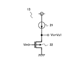
次に、第一レベルシフタ13の構成について説明する。図2は、第一レベルシフタを示す回路図である。
Next, the configuration of the
第一レベルシフタ13は、電流源21、及び、PMOSトランジスタ22を備える。PMOSトランジスタ22のゲートは第一レベルシフタ13の入力端子に接続され、ソースは第一レベルシフタ13の出力端子に接続され、ドレインは接地端子に接続される。電流源21は、電源端子と第一レベルシフタ13の出力端子との間に設けられる。
The
次に、第二レベルシフタ14の構成について説明する。図3は、第二レベルシフタを示す回路図である。
Next, the configuration of the
第二レベルシフタ14は、電流源31、及び、NMOSトランジスタ32を備える。NMOSトランジスタ32のゲートは第二レベルシフタ14の入力端子に接続され、ソースは第二レベルシフタ14の出力端子に接続され、ドレインは電源端子に接続される。電流源31は、第二レベルシフタ14の出力端子と接地端子との間に設けられる。
The
次に、ゲート電圧選択回路15の構成について説明する。図4は、ゲート電圧選択回路を示す回路図である。
Next, the configuration of the gate
ゲート電圧選択回路15は、スイッチ41〜44、及び、インバータ45を備える。また、ゲート電圧選択回路15は、第一入力端子IN1、第二入力端子IN2、制御端子CNT、及び、第一出力端子OUT1、第二出力端子OUT2を備える。
The gate
スイッチ41は、ゲート電圧選択回路15の第一入力端子IN1と第一出力端子OUT1との間に設けられ、電圧/Vcによって制御される。スイッチ42は、ゲート電圧選択回路15の第二入力端子IN2と第一出力端子OUT1との間に設けられ、電圧Vcによって制御される。スイッチ43は、ゲート電圧選択回路15の第一入力端子IN1と第二出力端子OUT2との間に設けられ、電圧Vcによって制御される。スイッチ44は、ゲート電圧選択回路15の第二入力端子IN2と第二出力端子OUT2との間に設けられ、電圧/Vcによって制御される。インバータ45の入力端子はゲート電圧選択回路15の制御端子CNTに接続される。インバータ45は、電圧Vcを入力され、電圧/Vcを出力する。スイッチ41〜44は、例えば図6のようにMOSトランジスタ61〜64で構成される。
The
次に、トランスミッションゲート10の動作について説明する。
入力端子INの入力電圧Vinは、第一レベルシフタ13の入力端子と第二レベルシフタ14の入力端子に入力される。
Next, the operation of the
The input voltage Vin of the input terminal IN is input to the input terminal of the
第一レベルシフタ13はソースフォロアであるので、PMOSトランジスタ22のソース電圧は電圧(Vin+Vs1)になる。電圧Vs1は、PMOSトランジスタ22の閾値電圧(−Vtp)の絶対値とオーバードライブ電圧Vo1との合計電圧である。第一レベルシフタ13は、この電圧(Vin+Vs1)を出力端子から出力する。
Since the
第二レベルシフタ14はソースフォロアであるので、NMOSトランジスタ32のソース電圧は電圧(Vin−Vs2)になる。電圧Vs2は、NMOSトランジスタ32の閾値電圧Vtnとオーバードライブ電圧Vo2との合計電圧である。第二レベルシフタ14は、この電圧(Vin−Vs2)を出力端子から出力する。
Since the
第一レベルシフタ13及び第二レベルシフタ14は、式(1)〜(3)が成立するようそれぞれ設計される。
Vtp=Vtn・・・(1)
Vo1=Vo2・・・(2)
Vs1=Vtp+Vo1=Vs2=Vtn+Vo2・・・(3)
ここで、制御端子CNTにハイレベルの電圧Vcが入力されているとすると、電圧/Vcはローレベルになる。すると、スイッチ42及び43がオンし、スイッチ41及びスイッチ44がオフする。よって、ゲート電圧選択回路15は、第二入力端子IN2の電圧(Vin−Vs2)つまり電圧(Vin−Vs1)を第一出力端子OUT1から出力する。また、ゲート電圧選択回路15は、第一入力端子IN1の電圧(Vin+Vs1)を第二出力端子OUT2から出力する。
The
Vtp = Vtn (1)
Vo1 = Vo2 (2)
Vs1 = Vtp + Vo1 = Vs2 = Vtn + Vo2 (3)
Here, assuming that a high level voltage Vc is input to the control terminal CNT, the voltage / Vc becomes a low level. Then, the
従って、PMOSトランジスタ11はゲート電圧が電圧(Vin−Vs1)になり、PMOSトランジスタ11のゲート・ソース間電圧Vgspは次式(4)で表される。
Vgsp=−Vs1=−(Vtp+Vo1)・・・(4)
PMOSトランジスタ11のゲート・ソース間電圧Vgspは閾値電圧(−Vtp)よりも低くなるので、PMOSトランジスタ11はオンする。
Accordingly, the gate voltage of the
Vgsp = −Vs1 = − (Vtp + Vo1) (4)
Since the gate-source voltage Vgsp of the
また、NMOSトランジスタ12はゲート電圧が電圧(Vin+Vs1)になり、NMOSトランジスタ12のゲート・ソース間電圧Vgsnは次式(5)で表される。
Vgsn=Vs2=Vtn+Vo2=Vs1=Vtp+Vo1・・・(5)
NMOSトランジスタ12のゲート・ソース間電圧Vgsnは閾値電圧Vtnよりも高くなるので、NMOSトランジスタ12はオンする。
Further, the gate voltage of the
Vgsn = Vs2 = Vtn + Vo2 = Vs1 = Vtp + Vo1 (5)
Since the gate-source voltage Vgsn of the
よって、トランスミッションゲート10は導通状態になり、出力端子OUTに入力電圧Vinを出力電圧Voutとして出力する。
Therefore, the
次に、制御端子CNTにローレベルの電圧Vcが入力されているとすると、電圧/Vcはハイレベルになる。すると、スイッチ42〜43がオフし、スイッチ41及びスイッチ44がオンする。よって、ゲート電圧選択回路15は、第一入力端子IN1の電圧(Vin+Vs1)を第一出力端子OUT1から出力する。また、ゲート電圧選択回路15は、第二入力端子IN2の電圧(Vin−Vs2)つまり電圧(Vin−Vs1)を第二出力端子OUT2から出力する。
Next, assuming that the low level voltage Vc is input to the control terminal CNT, the voltage / Vc becomes high level. Then, the
従って、PMOSトランジスタ11は、ゲート電圧が電圧(Vin+Vs1)になり、PMOSトランジスタ11のゲート・ソース間電圧Vgspは次式(6)で表される。
Vgsp=Vs1=Vtp+Vo1・・・(6)
PMOSトランジスタ11のゲート・ソース間電圧Vgspは閾値電圧(−Vtp)よりも高くなるので、PMOSトランジスタ11はオフする。
Therefore, the gate voltage of the
Vgsp = Vs1 = Vtp + Vo1 (6)
Since the gate-source voltage Vgsp of the
また、NMOSトランジスタ12はゲート電圧が電圧(Vin−Vs1)になり、NMOSトランジスタ12のゲート・ソース間電圧Vgsnは次式(7)で表される。
Vgsn=−Vs2=−(Vtn+Vo2)=−Vs1=−(Vtp+Vo1)・・・(7)
NMOSトランジスタ12のゲート・ソース間電圧Vgsnは閾値電圧Vtnよりも低くなるので、NMOSトランジスタ12はオフする。
Further, the gate voltage of the
Vgsn = −Vs2 = − (Vtn + Vo2) = − Vs1 = − (Vtp + Vo1) (7)
Since the gate-source voltage Vgsn of the
よって、トランスミッションゲート10は非導通になり、出力端子OUTに入力電圧Vinを出力電圧Voutとして出力しない。
Therefore, the
ここで、トランスミッションゲート10は、PMOSトランジスタ11とNMOSトランジスタ12のゲート長とゲート幅とゲート酸化膜厚をそれぞれ等しくなるようにする。すると、PMOSトランジスタ11のゲート・ソース間容量CgspとNMOSトランジスタ12のゲート・ソース間容量Cgsnとは等しくなる。また、式(1)より、PMOSトランジスタ11の閾値電圧VtpとNMOSトランジスタ12の閾値電圧Vtnとは等しい。また、電圧Vcがハイレベルのときは、式(4)〜(5)よりPMOSトランジスタ11のゲート・ソース間電圧Vgspの絶対値とNMOSトランジスタ12のゲート・ソース間電圧Vgsnとは等しい。
Here, the
上述のように構成したトランスミッションゲート10は、従来の技術で示した式(11)に基づく式(8)が成立するので、クロックフィードスルーの影響が低減し、高S/N特性が実現される。
(|Vgsp|−|Vtp|)・Cgsp/(Cgsp+Ch)
=(Vgsn−Vtn)・Cgsn/(Cgsn+Ch)・・・(8)
CgspはPMOSトランジスタ11のゲート・ソース間容量、CgsnはNMOSトランジスタ12のゲート・ソース間容量、Chは出力端子寄生容量である。
In the
(| Vgsp | − | Vtp |) · Cgsp / (Cgsp + Ch)
= (Vgsn−Vtn) · Cgsn / (Cgsn + Ch) (8)
Cgsp is a gate-source capacitance of the
また、式(2)と式(4)〜(5)と式(8)とより、次式(9)が成立する。
Cgsp/(Cgsp+Ch)=Cgsn/(Cgsn+Ch)・・・(9)
この式(9)は入力電圧Vinに依存しない。すなわち、トランスミッションゲート10は、入力電圧Vinの電圧値に関係なくクロックフィードスルーの影響が低減し、高S/N特性が実現される。
Moreover, following Formula (9) is materialized from Formula (2), Formula (4)-(5), and Formula (8).
Cgsp / (Cgsp + Ch) = Cgsn / (Cgsn + Ch) (9)
This equation (9) does not depend on the input voltage Vin. That is, in the
このようにすると、トランスミッションゲート10を構成するMOSトランジスタのゲート電圧は入力電圧Vinに基づいた電圧になることにより、入力電圧Vinが変動してもクロックフィードスルーの影響が低減でき、高S/N特性を実現できる。
In this way, the gate voltage of the MOS transistor constituting the
なお、ゲート電圧選択回路15は図4の回路に限定されるものではなく、例えば図5のように構成した回路であっても良い。
The gate
図5のゲート電圧選択回路は、PMOSトランジスタ51及び52、NMOSトランジスタ53及び54を備える。また、この回路は、第一入力端子IN1、第二入力端子IN2、制御端子CNT、及び、第一出力端子OUT1、第二出力端子OUT2を備える。
The gate voltage selection circuit of FIG. 5 includes
PMOSトランジスタ51及びNMOSトランジスタ53は、電圧(Vin+Vs1)を電源電圧として電圧(Vin−Vs2)を接地電圧とした第一のインバータを構成する。PMOSトランジスタ52及びNMOSトランジスタ54は、電圧(Vin+Vs1)を電源電圧として電圧(Vin−Vs2)を接地電圧とした第二のインバータを構成し、第一のインバータの後段に設けられる。第一のインバータは、入力端子をゲート電圧選択回路15の制御端子CNTに接続され、出力端子をゲート電圧選択回路15の第一出力端子OUT1に接続される。第二のインバータは、入力端子をゲート電圧選択回路15の第一出力端子OUT1に接続され、出力端子をゲート電圧選択回路15の第二出力端子OUT2に接続される。
The
また、第一レベルシフタ13及び第二レベルシフタ14は、電流源21及び電流源31を用いたが、図示しないが、抵抗を用いても良い。
Moreover, although the
また、第一レベルシフタ13及び第二レベルシフタ14は、一例として図2及び図3に示す回路としたが、入力電圧Vinを入力してVin±Vs1を出力する回路であればよい。例えば、図7に示すようにバッファアンプで構成しても良い。
Further, the
10 トランスミッションゲート
11 PMOSトランジスタ
12 NMOSトランジスタ
13 第一レベルシフタ
14 第二レベルシフタ
15 ゲート電圧選択回路
71 アンプ
DESCRIPTION OF
Claims (3)
前記入力電圧に所定電圧が加算された第一電圧を出力する第一レベルシフタと、
前記入力電圧から前記所定電圧が減算された第二電圧を出力する第二レベルシフタと、
前記第一電圧と前記第二電圧が入力され、前記第一電圧と前記第二電圧を切替えて相補的に出力する第一出力端子と第二出力端子を有するゲート電圧選択回路と、
前記第一出力端子がゲートに接続されたPMOSトランジスタと、
前記第二出力端子がゲートに接続されたNMOSトランジスタと、を備え、
前記PMOSトランジスタと前記NMOSトランジスタは、ゲート長とゲート幅とゲート酸化膜厚と閾値電圧の絶対値とが等しい、ことを特徴とするトランスミッションゲート。 A transmission gate that outputs an input voltage input from an input terminal from an output terminal,
A first level shifter that outputs a first voltage obtained by adding a predetermined voltage to the input voltage;
A second level shifter that outputs a second voltage obtained by subtracting the predetermined voltage from the input voltage;
A gate voltage selection circuit having a first output terminal and a second output terminal for inputting the first voltage and the second voltage, switching the first voltage and the second voltage, and outputting them in a complementary manner;
A PMOS transistor having the first output terminal connected to the gate;
An NMOS transistor having the second output terminal connected to the gate;
The transmission gate, wherein the PMOS transistor and the NMOS transistor have the same gate length, gate width, gate oxide film thickness, and absolute value of threshold voltage.
前記第二レベルシフタは、前記入力電圧がゲートに入力された第二のNMOSトランジスタを有し、
前記第二のPMOSトランジスタと前記第二のNMOSトランジスタは、閾値電圧の絶対値とオーバードライブ電圧が等しく、
前記所定電圧は、該閾値電圧の絶対値と該オーバードライブ電圧の和である、ことを特徴とする請求項1記載のトランスミッションゲート。 The first level shifter includes a second PMOS transistor having the input voltage input to the gate,
The second level shifter includes a second NMOS transistor in which the input voltage is input to a gate,
The second PMOS transistor and the second NMOS transistor have the same absolute value of the threshold voltage and the overdrive voltage,
The transmission gate according to claim 1, wherein the predetermined voltage is a sum of an absolute value of the threshold voltage and the overdrive voltage.
Priority Applications (5)
| Application Number | Priority Date | Filing Date | Title |
|---|---|---|---|
| JP2010026931A JP5431992B2 (en) | 2010-02-09 | 2010-02-09 | Transmission gate and semiconductor device |
| TW100103453A TWI530096B (en) | 2010-02-09 | 2011-01-28 | Transmission and semiconductor devices |
| US13/022,338 US8354873B2 (en) | 2010-02-09 | 2011-02-07 | Transmission gate and semiconductor device |
| KR1020110010961A KR101727752B1 (en) | 2010-02-09 | 2011-02-08 | Transmission gate and semiconductor device |
| CN201110039437.2A CN102195637B (en) | 2010-02-09 | 2011-02-09 | Transmission gate and semiconductor device |
Applications Claiming Priority (1)
| Application Number | Priority Date | Filing Date | Title |
|---|---|---|---|
| JP2010026931A JP5431992B2 (en) | 2010-02-09 | 2010-02-09 | Transmission gate and semiconductor device |
Publications (3)
| Publication Number | Publication Date |
|---|---|
| JP2011166449A JP2011166449A (en) | 2011-08-25 |
| JP2011166449A5 JP2011166449A5 (en) | 2013-02-07 |
| JP5431992B2 true JP5431992B2 (en) | 2014-03-05 |
Family
ID=44353216
Family Applications (1)
| Application Number | Title | Priority Date | Filing Date |
|---|---|---|---|
| JP2010026931A Expired - Fee Related JP5431992B2 (en) | 2010-02-09 | 2010-02-09 | Transmission gate and semiconductor device |
Country Status (5)
| Country | Link |
|---|---|
| US (1) | US8354873B2 (en) |
| JP (1) | JP5431992B2 (en) |
| KR (1) | KR101727752B1 (en) |
| CN (1) | CN102195637B (en) |
| TW (1) | TWI530096B (en) |
Families Citing this family (14)
| Publication number | Priority date | Publication date | Assignee | Title |
|---|---|---|---|---|
| US8461905B2 (en) * | 2009-01-07 | 2013-06-11 | Zentrum Mikroelektronic Dresden Ag | Adaptive bootstrap circuit for controlling CMOS switch(es) |
| JP5923919B2 (en) * | 2011-10-11 | 2016-05-25 | 株式会社ソシオネクスト | Semiconductor device and analog switch control method |
| TWI473072B (en) * | 2013-06-24 | 2015-02-11 | Orise Technology Co Ltd | Source driver with reduced number of latch devices |
| CN104426528B (en) * | 2013-09-11 | 2019-05-07 | 台湾积体电路制造股份有限公司 | Multivoltage input buffer and its correlation technique |
| JP2016139390A (en) * | 2015-01-23 | 2016-08-04 | エスアイアイ・セミコンダクタ株式会社 | Detection circuit |
| US9843322B2 (en) * | 2016-03-11 | 2017-12-12 | Texas Instruments Incorporated | Integrated high-side driver for P-N bimodal power device |
| KR101675573B1 (en) * | 2016-03-21 | 2016-11-11 | 주식회사 이노액시스 | Level Shifter, Digital Analog Converter, Buffer Amplifier and Source Driver and Electronic Device Including the Same |
| TWI653732B (en) | 2017-09-19 | 2019-03-11 | 世界先進積體電路股份有限公司 | Control circuit and operation circuit |
| CN109560536B (en) * | 2017-09-26 | 2021-01-05 | 世界先进积体电路股份有限公司 | Control circuit and operation circuit |
| US10818653B2 (en) | 2017-12-12 | 2020-10-27 | Vanguard International Semiconductor Corporation | Control circuit and operating circuit utilizing the same |
| CN108199701B (en) * | 2017-12-28 | 2021-05-07 | 清华大学 | High-speed CMOS transmission gate switch circuit |
| US10763846B1 (en) * | 2019-08-23 | 2020-09-01 | Nxp Usa, Inc. | High voltage tolerant analog switch |
| EP3799309A1 (en) | 2019-09-26 | 2021-03-31 | Ams Ag | Electric circuitry for signal transmission |
| US20220311439A1 (en) * | 2021-03-24 | 2022-09-29 | Stmicroelectronics International N.V. | Multiplexer circuit using a transmission gate circuit with a selectively boosted switch control signal |
Family Cites Families (15)
| Publication number | Priority date | Publication date | Assignee | Title |
|---|---|---|---|---|
| US4740717A (en) * | 1986-11-25 | 1988-04-26 | North American Philips Corporation, Signetics Division | Switching device with dynamic hysteresis |
| JPH01175410A (en) * | 1987-12-29 | 1989-07-11 | Sharp Corp | Semiconductor analog switch |
| JPH0595262A (en) * | 1991-03-30 | 1993-04-16 | Nec Corp | Analog input circuit |
| US5194768A (en) * | 1992-03-27 | 1993-03-16 | Advanced Micro Devices, Inc. | Apparatus for filtering noise from a periodic signal |
| JPH06208423A (en) * | 1993-01-12 | 1994-07-26 | Mitsubishi Electric Corp | Power supply circuit |
| JPH07169292A (en) | 1993-12-13 | 1995-07-04 | Matsushita Electron Corp | Cmos sample-and-hold circuit |
| JPH07221642A (en) * | 1994-02-02 | 1995-08-18 | Hitachi Ltd | Semiconductor integrated circuit |
| US6433613B1 (en) * | 2000-12-15 | 2002-08-13 | Fairchild Semiconductor Corporation | Translating switch circuit with disabling option |
| US6693479B1 (en) * | 2002-06-06 | 2004-02-17 | Analog Devices, Inc. | Boost structures for switched-capacitor systems |
| JP3949027B2 (en) * | 2002-08-06 | 2007-07-25 | 富士通株式会社 | Analog switch circuit |
| FR2894373B1 (en) * | 2005-12-07 | 2008-01-04 | Atmel Corp | AUTONOMOUS ANTI-FUSE CELL |
| JP4828343B2 (en) * | 2006-07-28 | 2011-11-30 | 三菱電機株式会社 | Analog switch circuit |
| JP5018245B2 (en) * | 2007-05-31 | 2012-09-05 | 株式会社日立製作所 | Analog switch |
| JP2009017276A (en) * | 2007-07-05 | 2009-01-22 | Nec Electronics Corp | Semiconductor device |
| JP2009108911A (en) * | 2007-10-29 | 2009-05-21 | Akira Koyama | Thread fixing mechanism and thread fixing method |
-
2010
- 2010-02-09 JP JP2010026931A patent/JP5431992B2/en not_active Expired - Fee Related
-
2011
- 2011-01-28 TW TW100103453A patent/TWI530096B/en not_active IP Right Cessation
- 2011-02-07 US US13/022,338 patent/US8354873B2/en active Active
- 2011-02-08 KR KR1020110010961A patent/KR101727752B1/en active IP Right Grant
- 2011-02-09 CN CN201110039437.2A patent/CN102195637B/en not_active Expired - Fee Related
Also Published As
| Publication number | Publication date |
|---|---|
| TWI530096B (en) | 2016-04-11 |
| CN102195637B (en) | 2015-07-01 |
| US20110193615A1 (en) | 2011-08-11 |
| US8354873B2 (en) | 2013-01-15 |
| TW201212537A (en) | 2012-03-16 |
| CN102195637A (en) | 2011-09-21 |
| KR101727752B1 (en) | 2017-04-17 |
| KR20110093661A (en) | 2011-08-18 |
| JP2011166449A (en) | 2011-08-25 |
Similar Documents
| Publication | Publication Date | Title |
|---|---|---|
| JP5431992B2 (en) | Transmission gate and semiconductor device | |
| KR101355684B1 (en) | Reference voltage circuit and electronic device | |
| JP4128545B2 (en) | Sampling switch | |
| WO2009081619A1 (en) | Buffer and display device | |
| JP2011060876A (en) | Semiconductor apparatus and breakdown voltage control method of the same | |
| US7492210B2 (en) | Voltage selection circuit | |
| US6924702B2 (en) | Low supply voltage and self-biased high speed receiver | |
| US8159301B1 (en) | Differential amplifier with hysteresis | |
| US7355450B1 (en) | Differential input buffers for low power supply | |
| JP6399938B2 (en) | Differential output buffer | |
| US20120068755A1 (en) | Level shifter | |
| JP2007067819A (en) | Delay adjusting circuit and synchronous type semiconductor device equipped with the circuit | |
| JP6363891B2 (en) | Analog switch circuit and selector circuit | |
| JP5290015B2 (en) | Buffer circuit | |
| JP2012114610A (en) | Electronic circuit | |
| US9374047B2 (en) | Buffer circuit | |
| KR102613131B1 (en) | CMOS inverter circuit | |
| JP2014165707A (en) | Semiconductor switch circuit | |
| US20060181313A1 (en) | Transistor logic circuit | |
| US8723581B1 (en) | Input buffers | |
| JP5203809B2 (en) | Current mirror circuit | |
| JP6610223B2 (en) | Semiconductor integrated circuit | |
| JP2015002507A (en) | Switch circuit | |
| KR20000074289A (en) | Level shifter for high voltage integrated circuits | |
| WO2012132281A1 (en) | Level shift circuit and semiconductor device |
Legal Events
| Date | Code | Title | Description |
|---|---|---|---|
| A521 | Request for written amendment filed |
Free format text: JAPANESE INTERMEDIATE CODE: A523 Effective date: 20121211 |
|
| A621 | Written request for application examination |
Free format text: JAPANESE INTERMEDIATE CODE: A621 Effective date: 20121211 |
|
| A977 | Report on retrieval |
Free format text: JAPANESE INTERMEDIATE CODE: A971007 Effective date: 20131025 |
|
| TRDD | Decision of grant or rejection written | ||
| A01 | Written decision to grant a patent or to grant a registration (utility model) |
Free format text: JAPANESE INTERMEDIATE CODE: A01 Effective date: 20131119 |
|
| A61 | First payment of annual fees (during grant procedure) |
Free format text: JAPANESE INTERMEDIATE CODE: A61 Effective date: 20131205 |
|
| R150 | Certificate of patent or registration of utility model |
Free format text: JAPANESE INTERMEDIATE CODE: R150 Ref document number: 5431992 Country of ref document: JP Free format text: JAPANESE INTERMEDIATE CODE: R150 |
|
| S111 | Request for change of ownership or part of ownership |
Free format text: JAPANESE INTERMEDIATE CODE: R313113 |
|
| R350 | Written notification of registration of transfer |
Free format text: JAPANESE INTERMEDIATE CODE: R350 |
|
| R250 | Receipt of annual fees |
Free format text: JAPANESE INTERMEDIATE CODE: R250 |
|
| R250 | Receipt of annual fees |
Free format text: JAPANESE INTERMEDIATE CODE: R250 |
|
| S533 | Written request for registration of change of name |
Free format text: JAPANESE INTERMEDIATE CODE: R313533 |
|
| R350 | Written notification of registration of transfer |
Free format text: JAPANESE INTERMEDIATE CODE: R350 |
|
| R250 | Receipt of annual fees |
Free format text: JAPANESE INTERMEDIATE CODE: R250 |
|
| R250 | Receipt of annual fees |
Free format text: JAPANESE INTERMEDIATE CODE: R250 |
|
| LAPS | Cancellation because of no payment of annual fees |