JP5431777B2 - Manufacturing method of semiconductor device - Google Patents
Manufacturing method of semiconductor device Download PDFInfo
- Publication number
- JP5431777B2 JP5431777B2 JP2009101679A JP2009101679A JP5431777B2 JP 5431777 B2 JP5431777 B2 JP 5431777B2 JP 2009101679 A JP2009101679 A JP 2009101679A JP 2009101679 A JP2009101679 A JP 2009101679A JP 5431777 B2 JP5431777 B2 JP 5431777B2
- Authority
- JP
- Japan
- Prior art keywords
- wafer
- insulating film
- film pattern
- thickness
- back surface
- Prior art date
- Legal status (The legal status is an assumption and is not a legal conclusion. Google has not performed a legal analysis and makes no representation as to the accuracy of the status listed.)
- Active
Links
- 239000004065 semiconductor Substances 0.000 title claims description 77
- 238000004519 manufacturing process Methods 0.000 title claims description 38
- 238000000034 method Methods 0.000 claims description 96
- 230000008569 process Effects 0.000 claims description 70
- 229910052751 metal Inorganic materials 0.000 claims description 52
- 239000002184 metal Substances 0.000 claims description 52
- 238000000227 grinding Methods 0.000 claims description 12
- 239000000853 adhesive Substances 0.000 claims description 4
- 230000001070 adhesive effect Effects 0.000 claims description 4
- 239000010408 film Substances 0.000 description 173
- 235000012431 wafers Nutrition 0.000 description 150
- 230000015572 biosynthetic process Effects 0.000 description 21
- 238000004544 sputter deposition Methods 0.000 description 20
- 229910052581 Si3N4 Inorganic materials 0.000 description 17
- VYPSYNLAJGMNEJ-UHFFFAOYSA-N Silicium dioxide Chemical compound O=[Si]=O VYPSYNLAJGMNEJ-UHFFFAOYSA-N 0.000 description 17
- HQVNEWCFYHHQES-UHFFFAOYSA-N silicon nitride Chemical compound N12[Si]34N5[Si]62N3[Si]51N64 HQVNEWCFYHHQES-UHFFFAOYSA-N 0.000 description 17
- 238000005268 plasma chemical vapour deposition Methods 0.000 description 14
- 239000000758 substrate Substances 0.000 description 14
- 238000005530 etching Methods 0.000 description 13
- 230000003014 reinforcing effect Effects 0.000 description 13
- XUIMIQQOPSSXEZ-UHFFFAOYSA-N Silicon Chemical compound [Si] XUIMIQQOPSSXEZ-UHFFFAOYSA-N 0.000 description 12
- 229910052710 silicon Inorganic materials 0.000 description 12
- 239000010703 silicon Substances 0.000 description 12
- 229910052814 silicon oxide Inorganic materials 0.000 description 12
- 238000010586 diagram Methods 0.000 description 9
- 238000005468 ion implantation Methods 0.000 description 9
- 229910021421 monocrystalline silicon Inorganic materials 0.000 description 8
- 230000001681 protective effect Effects 0.000 description 8
- XAGFODPZIPBFFR-UHFFFAOYSA-N aluminium Chemical compound [Al] XAGFODPZIPBFFR-UHFFFAOYSA-N 0.000 description 7
- 239000007789 gas Substances 0.000 description 7
- 239000000463 material Substances 0.000 description 7
- 230000000116 mitigating effect Effects 0.000 description 7
- 230000002093 peripheral effect Effects 0.000 description 7
- 238000001179 sorption measurement Methods 0.000 description 7
- 229910052782 aluminium Inorganic materials 0.000 description 6
- 239000012790 adhesive layer Substances 0.000 description 5
- 239000011521 glass Substances 0.000 description 5
- 239000000523 sample Substances 0.000 description 5
- 238000000137 annealing Methods 0.000 description 4
- 239000012535 impurity Substances 0.000 description 4
- 238000001459 lithography Methods 0.000 description 4
- IJGRMHOSHXDMSA-UHFFFAOYSA-N Atomic nitrogen Chemical compound N#N IJGRMHOSHXDMSA-UHFFFAOYSA-N 0.000 description 3
- 239000002131 composite material Substances 0.000 description 3
- 229910001873 dinitrogen Inorganic materials 0.000 description 3
- 239000010410 layer Substances 0.000 description 3
- 229910021420 polycrystalline silicon Inorganic materials 0.000 description 3
- 229920005591 polysilicon Polymers 0.000 description 3
- 239000000377 silicon dioxide Substances 0.000 description 3
- 239000010409 thin film Substances 0.000 description 3
- WFKWXMTUELFFGS-UHFFFAOYSA-N tungsten Chemical compound [W] WFKWXMTUELFFGS-UHFFFAOYSA-N 0.000 description 3
- 229910052721 tungsten Inorganic materials 0.000 description 3
- 239000010937 tungsten Substances 0.000 description 3
- XKRFYHLGVUSROY-UHFFFAOYSA-N Argon Chemical compound [Ar] XKRFYHLGVUSROY-UHFFFAOYSA-N 0.000 description 2
- RYGMFSIKBFXOCR-UHFFFAOYSA-N Copper Chemical compound [Cu] RYGMFSIKBFXOCR-UHFFFAOYSA-N 0.000 description 2
- BOTDANWDWHJENH-UHFFFAOYSA-N Tetraethyl orthosilicate Chemical compound CCO[Si](OCC)(OCC)OCC BOTDANWDWHJENH-UHFFFAOYSA-N 0.000 description 2
- 230000004913 activation Effects 0.000 description 2
- 229910045601 alloy Inorganic materials 0.000 description 2
- 239000000956 alloy Substances 0.000 description 2
- 230000004888 barrier function Effects 0.000 description 2
- 239000005380 borophosphosilicate glass Substances 0.000 description 2
- 229910052802 copper Inorganic materials 0.000 description 2
- 239000010949 copper Substances 0.000 description 2
- 230000000694 effects Effects 0.000 description 2
- 230000005669 field effect Effects 0.000 description 2
- 239000011229 interlayer Substances 0.000 description 2
- 150000002500 ions Chemical class 0.000 description 2
- 229910044991 metal oxide Inorganic materials 0.000 description 2
- 150000004706 metal oxides Chemical class 0.000 description 2
- 238000005453 pelletization Methods 0.000 description 2
- 238000005546 reactive sputtering Methods 0.000 description 2
- 230000002787 reinforcement Effects 0.000 description 2
- 239000000126 substance Substances 0.000 description 2
- 238000004381 surface treatment Methods 0.000 description 2
- 239000010936 titanium Substances 0.000 description 2
- 238000001039 wet etching Methods 0.000 description 2
- QGZKDVFQNNGYKY-UHFFFAOYSA-N Ammonia Chemical compound N QGZKDVFQNNGYKY-UHFFFAOYSA-N 0.000 description 1
- 229910001218 Gallium arsenide Inorganic materials 0.000 description 1
- OAICVXFJPJFONN-UHFFFAOYSA-N Phosphorus Chemical compound [P] OAICVXFJPJFONN-UHFFFAOYSA-N 0.000 description 1
- BLRPTPMANUNPDV-UHFFFAOYSA-N Silane Chemical compound [SiH4] BLRPTPMANUNPDV-UHFFFAOYSA-N 0.000 description 1
- 229910000577 Silicon-germanium Inorganic materials 0.000 description 1
- ATJFFYVFTNAWJD-UHFFFAOYSA-N Tin Chemical compound [Sn] ATJFFYVFTNAWJD-UHFFFAOYSA-N 0.000 description 1
- RTAQQCXQSZGOHL-UHFFFAOYSA-N Titanium Chemical compound [Ti] RTAQQCXQSZGOHL-UHFFFAOYSA-N 0.000 description 1
- 239000000654 additive Substances 0.000 description 1
- 229910052786 argon Inorganic materials 0.000 description 1
- 230000008901 benefit Effects 0.000 description 1
- 239000003990 capacitor Substances 0.000 description 1
- 150000001875 compounds Chemical class 0.000 description 1
- 239000013078 crystal Substances 0.000 description 1
- 238000005520 cutting process Methods 0.000 description 1
- 238000000151 deposition Methods 0.000 description 1
- 230000008021 deposition Effects 0.000 description 1
- 238000005516 engineering process Methods 0.000 description 1
- 229940104869 fluorosilicate Drugs 0.000 description 1
- 230000012447 hatching Effects 0.000 description 1
- 239000012212 insulator Substances 0.000 description 1
- 230000000873 masking effect Effects 0.000 description 1
- 239000000203 mixture Substances 0.000 description 1
- 238000012986 modification Methods 0.000 description 1
- 230000004048 modification Effects 0.000 description 1
- 238000002161 passivation Methods 0.000 description 1
- 229910052698 phosphorus Inorganic materials 0.000 description 1
- 239000011574 phosphorus Substances 0.000 description 1
- 239000011148 porous material Substances 0.000 description 1
- 239000012495 reaction gas Substances 0.000 description 1
- 239000003870 refractory metal Substances 0.000 description 1
- 230000007261 regionalization Effects 0.000 description 1
- 238000000926 separation method Methods 0.000 description 1
- 239000005368 silicate glass Substances 0.000 description 1
- 229910052719 titanium Inorganic materials 0.000 description 1
- 239000011800 void material Substances 0.000 description 1
Images


Classifications
-
- H—ELECTRICITY
- H01—ELECTRIC ELEMENTS
- H01L—SEMICONDUCTOR DEVICES NOT COVERED BY CLASS H10
- H01L29/00—Semiconductor devices adapted for rectifying, amplifying, oscillating or switching, or capacitors or resistors with at least one potential-jump barrier or surface barrier, e.g. PN junction depletion layer or carrier concentration layer; Details of semiconductor bodies or of electrodes thereof ; Multistep manufacturing processes therefor
- H01L29/66—Types of semiconductor device ; Multistep manufacturing processes therefor
- H01L29/68—Types of semiconductor device ; Multistep manufacturing processes therefor controllable by only the electric current supplied, or only the electric potential applied, to an electrode which does not carry the current to be rectified, amplified or switched
- H01L29/70—Bipolar devices
- H01L29/72—Transistor-type devices, i.e. able to continuously respond to applied control signals
- H01L29/739—Transistor-type devices, i.e. able to continuously respond to applied control signals controlled by field-effect, e.g. bipolar static induction transistors [BSIT]
- H01L29/7393—Insulated gate bipolar mode transistors, i.e. IGBT; IGT; COMFET
- H01L29/7395—Vertical transistors, e.g. vertical IGBT
-
- H—ELECTRICITY
- H01—ELECTRIC ELEMENTS
- H01L—SEMICONDUCTOR DEVICES NOT COVERED BY CLASS H10
- H01L21/00—Processes or apparatus adapted for the manufacture or treatment of semiconductor or solid state devices or of parts thereof
- H01L21/02—Manufacture or treatment of semiconductor devices or of parts thereof
- H01L21/04—Manufacture or treatment of semiconductor devices or of parts thereof the devices having at least one potential-jump barrier or surface barrier, e.g. PN junction, depletion layer or carrier concentration layer
- H01L21/18—Manufacture or treatment of semiconductor devices or of parts thereof the devices having at least one potential-jump barrier or surface barrier, e.g. PN junction, depletion layer or carrier concentration layer the devices having semiconductor bodies comprising elements of Group IV of the Periodic System or AIIIBV compounds with or without impurities, e.g. doping materials
- H01L21/30—Treatment of semiconductor bodies using processes or apparatus not provided for in groups H01L21/20 - H01L21/26
- H01L21/302—Treatment of semiconductor bodies using processes or apparatus not provided for in groups H01L21/20 - H01L21/26 to change their surface-physical characteristics or shape, e.g. etching, polishing, cutting
- H01L21/306—Chemical or electrical treatment, e.g. electrolytic etching
- H01L21/308—Chemical or electrical treatment, e.g. electrolytic etching using masks
- H01L21/3083—Chemical or electrical treatment, e.g. electrolytic etching using masks characterised by their size, orientation, disposition, behaviour, shape, in horizontal or vertical plane
-
- H—ELECTRICITY
- H01—ELECTRIC ELEMENTS
- H01L—SEMICONDUCTOR DEVICES NOT COVERED BY CLASS H10
- H01L21/00—Processes or apparatus adapted for the manufacture or treatment of semiconductor or solid state devices or of parts thereof
- H01L21/67—Apparatus specially adapted for handling semiconductor or electric solid state devices during manufacture or treatment thereof; Apparatus specially adapted for handling wafers during manufacture or treatment of semiconductor or electric solid state devices or components ; Apparatus not specifically provided for elsewhere
- H01L21/683—Apparatus specially adapted for handling semiconductor or electric solid state devices during manufacture or treatment thereof; Apparatus specially adapted for handling wafers during manufacture or treatment of semiconductor or electric solid state devices or components ; Apparatus not specifically provided for elsewhere for supporting or gripping
- H01L21/6835—Apparatus specially adapted for handling semiconductor or electric solid state devices during manufacture or treatment thereof; Apparatus specially adapted for handling wafers during manufacture or treatment of semiconductor or electric solid state devices or components ; Apparatus not specifically provided for elsewhere for supporting or gripping using temporarily an auxiliary support
-
- H—ELECTRICITY
- H01—ELECTRIC ELEMENTS
- H01L—SEMICONDUCTOR DEVICES NOT COVERED BY CLASS H10
- H01L21/00—Processes or apparatus adapted for the manufacture or treatment of semiconductor or solid state devices or of parts thereof
- H01L21/70—Manufacture or treatment of devices consisting of a plurality of solid state components formed in or on a common substrate or of parts thereof; Manufacture of integrated circuit devices or of parts thereof
- H01L21/77—Manufacture or treatment of devices consisting of a plurality of solid state components or integrated circuits formed in, or on, a common substrate
- H01L21/78—Manufacture or treatment of devices consisting of a plurality of solid state components or integrated circuits formed in, or on, a common substrate with subsequent division of the substrate into plural individual devices
-
- H—ELECTRICITY
- H01—ELECTRIC ELEMENTS
- H01L—SEMICONDUCTOR DEVICES NOT COVERED BY CLASS H10
- H01L22/00—Testing or measuring during manufacture or treatment; Reliability measurements, i.e. testing of parts without further processing to modify the parts as such; Structural arrangements therefor
- H01L22/10—Measuring as part of the manufacturing process
- H01L22/14—Measuring as part of the manufacturing process for electrical parameters, e.g. resistance, deep-levels, CV, diffusions by electrical means
-
- H—ELECTRICITY
- H01—ELECTRIC ELEMENTS
- H01L—SEMICONDUCTOR DEVICES NOT COVERED BY CLASS H10
- H01L29/00—Semiconductor devices adapted for rectifying, amplifying, oscillating or switching, or capacitors or resistors with at least one potential-jump barrier or surface barrier, e.g. PN junction depletion layer or carrier concentration layer; Details of semiconductor bodies or of electrodes thereof ; Multistep manufacturing processes therefor
- H01L29/66—Types of semiconductor device ; Multistep manufacturing processes therefor
- H01L29/66007—Multistep manufacturing processes
- H01L29/66075—Multistep manufacturing processes of devices having semiconductor bodies comprising group 14 or group 13/15 materials
- H01L29/66227—Multistep manufacturing processes of devices having semiconductor bodies comprising group 14 or group 13/15 materials the devices being controllable only by the electric current supplied or the electric potential applied, to an electrode which does not carry the current to be rectified, amplified or switched, e.g. three-terminal devices
- H01L29/66234—Bipolar junction transistors [BJT]
- H01L29/66325—Bipolar junction transistors [BJT] controlled by field-effect, e.g. insulated gate bipolar transistors [IGBT]
- H01L29/66333—Vertical insulated gate bipolar transistors
-
- H—ELECTRICITY
- H01—ELECTRIC ELEMENTS
- H01L—SEMICONDUCTOR DEVICES NOT COVERED BY CLASS H10
- H01L2221/00—Processes or apparatus adapted for the manufacture or treatment of semiconductor or solid state devices or of parts thereof covered by H01L21/00
- H01L2221/67—Apparatus for handling semiconductor or electric solid state devices during manufacture or treatment thereof; Apparatus for handling wafers during manufacture or treatment of semiconductor or electric solid state devices or components; Apparatus not specifically provided for elsewhere
- H01L2221/683—Apparatus for handling semiconductor or electric solid state devices during manufacture or treatment thereof; Apparatus for handling wafers during manufacture or treatment of semiconductor or electric solid state devices or components; Apparatus not specifically provided for elsewhere for supporting or gripping
- H01L2221/68304—Apparatus for handling semiconductor or electric solid state devices during manufacture or treatment thereof; Apparatus for handling wafers during manufacture or treatment of semiconductor or electric solid state devices or components; Apparatus not specifically provided for elsewhere for supporting or gripping using temporarily an auxiliary support
- H01L2221/6834—Apparatus for handling semiconductor or electric solid state devices during manufacture or treatment thereof; Apparatus for handling wafers during manufacture or treatment of semiconductor or electric solid state devices or components; Apparatus not specifically provided for elsewhere for supporting or gripping using temporarily an auxiliary support used to protect an active side of a device or wafer
-
- H—ELECTRICITY
- H01—ELECTRIC ELEMENTS
- H01L—SEMICONDUCTOR DEVICES NOT COVERED BY CLASS H10
- H01L2924/00—Indexing scheme for arrangements or methods for connecting or disconnecting semiconductor or solid-state bodies as covered by H01L24/00
- H01L2924/0001—Technical content checked by a classifier
- H01L2924/0002—Not covered by any one of groups H01L24/00, H01L24/00 and H01L2224/00
-
- H—ELECTRICITY
- H01—ELECTRIC ELEMENTS
- H01L—SEMICONDUCTOR DEVICES NOT COVERED BY CLASS H10
- H01L2924/00—Indexing scheme for arrangements or methods for connecting or disconnecting semiconductor or solid-state bodies as covered by H01L24/00
- H01L2924/10—Details of semiconductor or other solid state devices to be connected
- H01L2924/11—Device type
- H01L2924/13—Discrete devices, e.g. 3 terminal devices
- H01L2924/1304—Transistor
- H01L2924/1305—Bipolar Junction Transistor [BJT]
- H01L2924/13055—Insulated gate bipolar transistor [IGBT]
-
- H—ELECTRICITY
- H01—ELECTRIC ELEMENTS
- H01L—SEMICONDUCTOR DEVICES NOT COVERED BY CLASS H10
- H01L2924/00—Indexing scheme for arrangements or methods for connecting or disconnecting semiconductor or solid-state bodies as covered by H01L24/00
- H01L2924/10—Details of semiconductor or other solid state devices to be connected
- H01L2924/11—Device type
- H01L2924/13—Discrete devices, e.g. 3 terminal devices
- H01L2924/1304—Transistor
- H01L2924/1306—Field-effect transistor [FET]
- H01L2924/13091—Metal-Oxide-Semiconductor Field-Effect Transistor [MOSFET]
-
- H—ELECTRICITY
- H01—ELECTRIC ELEMENTS
- H01L—SEMICONDUCTOR DEVICES NOT COVERED BY CLASS H10
- H01L2924/00—Indexing scheme for arrangements or methods for connecting or disconnecting semiconductor or solid-state bodies as covered by H01L24/00
- H01L2924/19—Details of hybrid assemblies other than the semiconductor or other solid state devices to be connected
- H01L2924/1901—Structure
- H01L2924/1904—Component type
- H01L2924/19041—Component type being a capacitor
Description
本発明は、半導体装置(または半導体集積回路装置)の製造方法におけるウエハ・ハンドリング技術に適用して有効な技術に関する。 The present invention relates to a technique effective when applied to a wafer handling technique in a method of manufacturing a semiconductor device (or a semiconductor integrated circuit device).
日本特開2003−243356号公報(特許文献1)には、縦型パワーMOSFET(Metal Oxide Semiconductor Field Effect Transistor)のオン抵抗を低くするためにウエハ裏面をエッチングする際、ウエハのわれや曲がりを防止するために、ウエハの周辺にシール部材を当てることで、周辺部を厚いまま残す技術が開示されている。 In Japanese Patent Laid-Open No. 2003-243356 (Patent Document 1), in order to reduce the on-resistance of a vertical power MOSFET (Metal Oxide Field Effect Transistor), the wafer is prevented from being bent or bent when the back surface of the wafer is etched. In order to do this, a technique is disclosed in which a peripheral member is left thick by applying a seal member to the periphery of the wafer.
日本特開2001−44088号公報(特許文献2)には、縦型パワー・デバイス用ウエハの強度と耐久性を改良するために、ウエハ裏面の周辺に窒化シリコン膜等でリム状のハード・マスクを形成し、それをマスクとしてエッチングすることで、周辺部を厚いまま残す技術が開示されている。なお、このハード・マスク等はエッチング後に除去している。 In Japanese Patent Laid-Open No. 2001-44088 (Patent Document 2), in order to improve the strength and durability of a wafer for vertical power devices, a rim-shaped hard mask is formed around the back surface of the wafer with a silicon nitride film or the like. A technique is disclosed in which the peripheral portion is left thick by forming the substrate and etching it as a mask. The hard mask and the like are removed after etching.
日本特開2007−317950号公報(特許文献3)には、半導体素子の製造工程において、シリコン・ウエハを薄膜化して処理する際に、ウエハの強度を確保するため、ウエハの周辺をリング状に厚いまま残すとともに、あらかじめウエハの裏面に格子状にシリコン酸化膜、窒化シリコン膜等を埋め込んでおき、それらを残すように、シリコン部分をエッチングして薄膜化する技術が開示されている。 Japanese Patent Application Laid-Open No. 2007-317950 (Patent Document 3) discloses that in the process of manufacturing a semiconductor device, when a silicon wafer is processed in a thin film, the periphery of the wafer is formed in a ring shape in order to ensure the strength of the wafer. A technique is disclosed in which a silicon oxide film, a silicon nitride film, or the like is embedded in a lattice shape on the back surface of the wafer in advance and the silicon portion is etched to reduce the thickness so as to leave them while leaving the wafer thick.
日本特開2005−322839号公報(特許文献4)または米国特許公開2005−0253235号公報(特許文献5)には、ウエハのそりを緩和するために、パターン化されたシリコン酸化膜、窒化シリコン膜等を形成する技術が開示されている。 Japanese Laid-Open Patent Publication No. 2005-322839 (Patent Document 4) or US Patent Publication No. 2005-0253235 (Patent Document 5) describes a patterned silicon oxide film and silicon nitride film to alleviate warpage of a wafer. Etc. are disclosed.
日本特開2007−335659号公報(特許文献6)および日本特開2008−53595号公報(特許文献7)には、ウエハの薄膜化の際に、窒化シリコン膜パターンをエッチングマスクとして用い、エッチング後に、その窒化シリコン膜パターンを除去する技術が開示されている。 In Japanese Unexamined Patent Application Publication No. 2007-335659 (Patent Document 6) and Japanese Unexamined Patent Application Publication No. 2008-53595 (Patent Document 7), a silicon nitride film pattern is used as an etching mask when a wafer is thinned. A technique for removing the silicon nitride film pattern is disclosed.
IGBT(Insulated Gate Bipolar Transistor)や縦型パワーMOSFET等に代表されるウエハの厚さが200μm未満の薄膜ウエハ状態で、種々の加工を繰り返す半導体プロセスにおいては、薄膜化以降の工程では、ウエハのデバイス面(表側主面)に補強用ガラス板を貼り付けた状態で処理を実行することが標準となっている。しかし、本願発明者が検討したところによると、製造コストの70%程度が、この補強用ガラス板に関するものであることが明らかとなった。 In a semiconductor process in which various processes are repeated in a thin film wafer state in which the thickness of the wafer is less than 200 μm, such as an IGBT (Insulated Gate Bipolar Transistor) and a vertical power MOSFET, a wafer device is used in the steps after thinning. It is standard to execute the treatment with a reinforcing glass plate attached to the surface (front side main surface). However, according to a study by the inventors of the present application, it has become clear that about 70% of the manufacturing cost relates to the reinforcing glass plate.
本願発明は、これらの課題を解決するためになされたものである。 The present invention has been made to solve these problems.
本発明の目的は、信頼性の高い半導体装置の製造プロセスを提供することにある。 An object of the present invention is to provide a manufacturing process of a highly reliable semiconductor device.
本発明の前記並びにその他の目的と新規な特徴は本明細書の記述及び添付図面から明らかになるであろう。 The above and other objects and novel features of the present invention will be apparent from the description of this specification and the accompanying drawings.
本願において開示される発明のうち代表的なものの概要を簡単に説明すれば下記の通りである。 The following is a brief description of an outline of typical inventions disclosed in the present application.
すなわち、本願の一つの発明は、ウエハのデバイス面(表側面)に対する処理がほぼ完了し、バック・グラインディングを施したウエハの裏面の周辺端部に応力緩和絶縁膜パターンを形成するものである。 That is, in one invention of the present application, the processing on the device surface (front side surface) of the wafer is almost completed, and the stress relaxation insulating film pattern is formed on the peripheral edge of the back surface of the wafer subjected to back grinding. .
本願において開示される発明のうち代表的なものによって得られる効果を簡単に説明すれば下記のとおりである。 The effects obtained by the representative ones of the inventions disclosed in the present application will be briefly described as follows.
すなわち、ウエハのデバイス面(表側面)に対する処理がほぼ完了し、バック・グラインディングを施したウエハの裏面の周辺端部に応力緩和絶縁膜パターンを形成することで、補強用ガラス板等の高価な材料を使用しなくとも、その後のウエハ処理をスムーズに実行できる。 That is, the processing on the device surface (front side) of the wafer is almost completed, and a stress relaxation insulating film pattern is formed on the peripheral edge of the back surface of the wafer subjected to back-grinding. Even if a new material is not used, the subsequent wafer processing can be executed smoothly.
〔実施の形態の概要〕
先ず、本願において開示される発明の代表的な実施の形態について概要を説明する。
[Outline of Embodiment]
First, an outline of a typical embodiment of the invention disclosed in the present application will be described.
1.以下の工程を含む半導体装置の製造方法:
(a)第1の厚さを有する半導体ウエハの第1の主面上に、第1の金属膜を形成する工程;
(b)前記工程(a)の後、前記半導体ウエハの第2の主面側に対して、バック・グラインディング処理を実行することにより、前記第1の厚さよりも薄い第2の厚さとする工程;
(c)前記工程(b)の後、前記半導体ウエハの前記第2の主面上に、その周辺に沿って、第1の絶縁膜からなり、前記第2の主面の周辺に沿う円環状絶縁膜パターンを含む絶縁膜パターンを形成する工程;
(d)前記絶縁膜パターンがある状態で、前記円環状絶縁膜パターンの開口部の厚さを前記第2の厚さよりも薄い第3の厚さとする工程;
(e)前記工程(d)の後、前記絶縁膜パターンがある状態で、前記半導体ウエハに対して、電気的テストを実行する工程;
(f)前記工程(e)の後、前記絶縁膜パターンがある状態で、前記半導体ウエハの前記第2の主面を粘着シートに貼り付けることにより、前記粘着シートを介してダイシング・フレームに保持させる工程;
(g)前記工程(f)の後、ダイシング・フレームに保持された状態で、前記半導体ウエハを個々のチップに分割する工程。
1. A semiconductor device manufacturing method including the following steps:
(A) forming a first metal film on a first main surface of a semiconductor wafer having a first thickness;
(B) After the step (a), by performing a back-grinding process on the second main surface side of the semiconductor wafer, a second thickness smaller than the first thickness is obtained. Process;
(C) After the step (b), an annular shape is formed on the second main surface of the semiconductor wafer along the periphery along the periphery of the semiconductor wafer and along the periphery of the second main surface. Forming an insulating film pattern including an insulating film pattern;
(D) a step of setting the thickness of the opening of the annular insulating film pattern to a third thickness smaller than the second thickness in a state where the insulating film pattern is present;
(E) after the step (d), performing an electrical test on the semiconductor wafer in a state where the insulating film pattern is present;
(F) After the step (e), the second main surface of the semiconductor wafer is attached to the adhesive sheet in a state where the insulating film pattern exists, and is held on the dicing frame via the adhesive sheet. The step of causing;
(G) After the step (f), the step of dividing the semiconductor wafer into individual chips while being held by a dicing frame.
2.前記1項の半導体装置の製造方法において、前記第1の絶縁膜は、前記半導体ウエハに作用する応力を緩和するような応力を有する。
2. In the method of manufacturing a semiconductor device according to the
3.前記1または2項の半導体装置の製造方法において、前記第1の絶縁膜は、CVDにより形成される。
3. In the method for manufacturing a semiconductor device according to
4.前記1または2項の半導体装置の製造方法において、前記第1の絶縁膜は、プラズマCVDにより形成される。
4). In the method for manufacturing a semiconductor device according to
5.前記1または2項の半導体装置の製造方法において、前記第1の絶縁膜は、スパッタリングにより形成される。
5. In the method for manufacturing a semiconductor device according to the
6.前記1から5項のいずれか一つの半導体装置の製造方法において、前記絶縁膜パターンは、前記半導体ウエハの外周に沿って、円環状を呈している。 6). 6. In the method of manufacturing a semiconductor device according to any one of 1 to 5, the insulating film pattern has an annular shape along an outer periphery of the semiconductor wafer.
7.前記1から6項のいずれか一つの半導体装置の製造方法において、前記第1の絶縁膜は無機絶縁膜である。 7). 7. The method for manufacturing a semiconductor device according to any one of 1 to 6, wherein the first insulating film is an inorganic insulating film.
8.前記1から7項のいずれか一つの半導体装置の製造方法において、前記第1の絶縁膜は窒化シリコン系絶縁膜である。 8). 8. The method of manufacturing a semiconductor device according to any one of 1 to 7, wherein the first insulating film is a silicon nitride insulating film.
9.前記1から8項のいずれか一つの半導体装置の製造方法において、前記第1の金属膜は、アルミニウム系、銅系、またはタングステン系のメタル膜である。 9. 9. In the method of manufacturing a semiconductor device according to any one of 1 to 8, the first metal film is an aluminum-based, copper-based, or tungsten-based metal film.
10.前記1から9項のいずれか一つの半導体装置の製造方法において、前記工程(d)の前記エッチングは、ウエット・エッチングである。 10. 10. The method for manufacturing a semiconductor device according to any one of 1 to 9, wherein the etching in the step (d) is wet etching.
11.前記1、2および5から10項のいずれか一つの半導体装置の製造方法において、前記絶縁膜パターンは、シャドー・マスクを用いたスパッタリングにより形成される。 11. 11. In the method for manufacturing a semiconductor device according to any one of 1, 2, and 5 to 10, the insulating film pattern is formed by sputtering using a shadow mask.
12.前記1から11項のいずれか一つの半導体装置の製造方法において、前記工程(e)の前記電気的テストは、ウエハ・テストである。 12 12. In the method for manufacturing a semiconductor device according to any one of 1 to 11, the electrical test in the step (e) is a wafer test.
13.前記1から12項のいずれか一つの半導体装置の製造方法において、前記半導体装置は、パワーMOSFETを有する。 13. In the method for manufacturing a semiconductor device according to any one of 1 to 12, the semiconductor device includes a power MOSFET.
14.前記1から12項のいずれか一つの半導体装置の製造方法において、前記半導体装置は、IGBTを有する。 14 In the method for manufacturing a semiconductor device according to any one of 1 to 12, the semiconductor device includes an IGBT.
15.前記1から14項のいずれか一つの半導体装置の製造方法において、前記半導体ウエハは、シリコン系ウエハである。 15. 15. The method for manufacturing a semiconductor device according to any one of 1 to 14, wherein the semiconductor wafer is a silicon wafer.
16.前記1から15項のいずれか一つの半導体装置の製造方法において、更に、以下の工程を含む:
(h)前記工程(e)の前であって前記工程(d)の後、前記絶縁膜パターンがある状態で、前記半導体ウエハの前記第2の主面上に、第2の金属膜を形成する工程。
16. 16. The method for manufacturing a semiconductor device according to any one of 1 to 15 further includes the following steps:
(H) Before the step (e) and after the step (d), a second metal film is formed on the second main surface of the semiconductor wafer with the insulating film pattern present Process.
17.前記16項の半導体装置の製造方法において、更に、以下の工程を含む:
(i)前記工程(h)の前であって前記工程(d)の後、前記絶縁膜パターンがある状態で、前記半導体ウエハの前記第2の主面に、不純物イオンを注入する工程。
17. The method for manufacturing a semiconductor device according to the
(I) A step of implanting impurity ions into the second main surface of the semiconductor wafer before the step (h) and after the step (d) in a state where the insulating film pattern is present.
18.前記17項の半導体装置の製造方法において、更に、以下の工程を含む:
(j)前記工程(h)の前であって前記工程(i)の後、前記絶縁膜パターンがある状態で、前記半導体ウエハの前記第2の主面に対して、前記不純物イオンの活性化アニールを実行する工程。
18. The method for manufacturing a semiconductor device according to the item 17, further includes the following steps:
(J) Before the step (h) and after the step (i), the impurity ions are activated with respect to the second main surface of the semiconductor wafer with the insulating film pattern. A process of performing annealing.
19.前記18項の半導体装置の製造方法において、更に、以下の工程を含む:
(k)前記工程(h)の前であって前記工程(j)の後、前記絶縁膜パターンがある状態で、前記半導体ウエハの前記第2の主面の前記開口部の酸化膜を除去する工程。
19. The method for manufacturing a semiconductor device according to the item 18, further includes the following steps:
(K) Before the step (h) and after the step (j), the oxide film in the opening on the second main surface of the semiconductor wafer is removed with the insulating film pattern present. Process.
20.前記1から19項のいずれか一つの半導体装置の製造方法において、前記第1の厚さは230マイクロ・メートル以上で且つ1ミリ・メートル未満であり、前記第2の厚さは70マイクロ・メートル以上で且つ230マイクロ・メートル未満であり、前記第3の厚さは200マイクロ・メートル未満で且つ30マイクロ・メートル以上である。 20. 20. The method of manufacturing a semiconductor device according to any one of 1 to 19, wherein the first thickness is not less than 230 micrometers and less than 1 millimeter, and the second thickness is 70 micrometers. And less than 230 micrometers, and the third thickness is less than 200 micrometers and greater than or equal to 30 micrometers.
〔本願における記載形式・基本的用語・用法の説明〕
1.本願において、実施の態様の記載は、必要に応じて、便宜上複数のセクションに分けて記載する場合もあるが、特にそうでない旨明示した場合を除き、これらは相互に独立別個のものではなく、単一の例の各部分、一方が他方の一部詳細または一部または全部の変形例等である。また、原則として、同様の部分は繰り返しを省略する。また、実施の態様における各構成要素は、特にそうでない旨明示した場合、理論的にその数に限定される場合および文脈から明らかにそうでない場合を除き、必須のものではない。
[Description format, basic terms, usage in this application]
1. In the present application, the description of the embodiment may be divided into a plurality of sections for convenience, if necessary, but these are not independent from each other unless otherwise specified. Each part of a single example, one part is the other part of the details, or part or all of the modifications. Moreover, as a general rule, the same part is not repeated. In addition, each component in the embodiment is not indispensable unless specifically stated otherwise, unless it is theoretically limited to the number, and obviously not in context.
更に、本願において、「半導体装置」というときは、主に、各種トランジスタ(能動素子)を中心に、抵抗、コンデンサ等を半導体チップ等(たとえば単結晶シリコン基板)上に集積したものをいう。ここで、各種トランジスタの代表的なものとしては、MOSFET(Metal Oxide Semiconductor Field Effect Transistor)に代表されるMISFET(Metal Insulator Semiconductor Field Effect Transistor)を例示することができる。 Further, in the present application, the term “semiconductor device” mainly refers to a device in which resistors, capacitors, and the like are integrated on a semiconductor chip or the like (for example, a single crystal silicon substrate) with various transistors (active elements) as the center. Here, as a representative of various transistors, a MISFET (Metal Insulator Semiconductor Effect Transistor) typified by a MOSFET (Metal Oxide Field Effect Transistor) can be exemplified.
2.同様に実施の態様等の記載において、材料、組成等について、「AからなるX」等といっても、特にそうでない旨明示した場合および文脈から明らかに、そうでない場合を除き、A以外の要素を主要な構成要素のひとつとするものを排除するものではない。たとえば、成分についていえば、「Aを主要な成分として含むX」等の意味である。たとえば、「シリコン部材」等といっても、純粋なシリコンに限定されるものではなく、SiGe合金やその他シリコンを主要な成分とする多元合金、その他の添加物等を含む部材も含むものであることはいうまでもない。同様に、「酸化シリコン膜」、「酸化シリコン系絶縁膜」等と言っても、比較的純粋な非ドープ酸化シリコン(Undoped Silicon Dioxide)だけでなく、FSG(Fluorosilicate Glass)、TEOSベース酸化シリコン(TEOS-based silicon oxide)、SiOC(Silicon Oxicarbide)またはカーボンドープ酸化シリコン(Carbon-doped Silicon oxide)またはOSG(Organosilicate glass)、PSG(Phosphorus Silicate Glass)、BPSG(Borophosphosilicate Glass)等の熱酸化膜、CVD酸化膜、SOG(Spin ON Glass)、ナノ・クラスタリング・シリカ(Nano-Clustering Silica:NSC)等の塗布系酸化シリコン、これらと同様な部材に空孔を導入したシリカ系Low-k絶縁膜(ポーラス系絶縁膜)、およびこれらを主要な構成要素とする他のシリコン系絶縁膜との複合膜等を含むことは言うまでもない。 2. Similarly, in the description of the embodiment and the like, the material, composition, etc. may be referred to as “X consisting of A”, etc., except when clearly stated otherwise and clearly from the context, except for A It does not exclude what makes an element one of the main components. For example, as for the component, it means “X containing A as a main component”. For example, “silicon member” is not limited to pure silicon, but also includes SiGe alloys, other multi-component alloys containing silicon as a main component, and members containing other additives. Needless to say. Similarly, “silicon oxide film”, “silicon oxide insulating film”, etc. are not only relatively pure undoped silicon oxide (FS), but also FSG (Fluorosilicate Glass), TEOS-based silicon oxide ( Thermal oxide films such as TEOS-based silicon oxide), SiOC (Silicon Oxicarbide) or carbon-doped silicon oxide or OSG (Organosilicate glass), PSG (Phosphorus Silicate Glass), BPSG (Borophosphosilicate Glass), CVD Oxide film, SOG (Spin ON Glass), nano-clustering silica (Nano-Clustering Silica: NSC), etc., coated silicon oxide, silica-based low-k insulating film (porous) with pores introduced in the same materials Needless to say, it includes a composite insulating film and other silicon-based insulating films having these as main components.
また、酸化シリコン系絶縁膜と並んで、半導体分野で常用されているシリコン系絶縁膜としては、窒化シリコン系絶縁膜がある。この系統の属する材料としては、SiN,SiCN,SiNH,SiCNH等がある。ここで、「窒化シリコン」というときは、特にそうでない旨明示したときを除き、SiNおよびSiNHの両方を含む。同様に、「SiCN」というときは、特にそうでない旨明示したときを除き、SiCNおよびSiCNHの両方を含む。 In addition to silicon oxide insulating films, silicon nitride insulating films that are commonly used in the semiconductor field include silicon nitride insulating films. Materials belonging to this system include SiN, SiCN, SiNH, SiCNH, and the like. Here, “silicon nitride” includes both SiN and SiNH unless otherwise specified. Similarly, “SiCN” includes both SiCN and SiCNH, unless otherwise specified.
なお、SiCは、SiNと類似の性質を有するが、SiONは、むしろ、酸化シリコン系絶縁膜に分類すべき場合が多い。 Note that SiC has similar properties to SiN, but SiON is often rather classified as a silicon oxide insulating film.
窒化シリコン膜は、SAC(Self−Aligned Contact)技術におけるエッチ・ストップ膜として、多用されるほか、SMT(Stress Memorization Technique)における応力付与膜としても使用される。 The silicon nitride film is frequently used as an etch stop film in SAC (Self-Aligned Contact) technology, and also used as a stress applying film in SMT (Stress Memory Technique).
3.同様に、図形、位置、属性等に関して、好適な例示をするが、特にそうでない旨明示した場合および文脈から明らかにそうでない場合を除き、厳密にそれに限定されるものではないことは言うまでもない。 3. Similarly, suitable examples of graphics, positions, attributes, and the like are given, but it is needless to say that the present invention is not strictly limited to those cases unless explicitly stated otherwise, and unless otherwise apparent from the context.
4.さらに、特定の数値、数量に言及したときも、特にそうでない旨明示した場合、理論的にその数に限定される場合および文脈から明らかにそうでない場合を除き、その特定の数値を超える数値であってもよいし、その特定の数値未満の数値でもよい。 4). In addition, when a specific number or quantity is mentioned, a numerical value exceeding that specific number will be used unless specifically stated otherwise, unless theoretically limited to that number, or unless otherwise clearly indicated by the context. There may be a numerical value less than the specific numerical value.
5.「ウエハ」というときは、通常は半導体装置(半導体集積回路装置、電子装置も同じ)をその上に形成する単結晶シリコン・ウエハを指すが、エピタキシャルウエハ、SOI基板、LCDガラス基板等の絶縁基板と半導体層等の複合ウエハ等も含むことは言うまでもない。 5. “Wafer” usually refers to a single crystal silicon wafer on which a semiconductor device (same as a semiconductor integrated circuit device and an electronic device) is formed, but an insulating substrate such as an epitaxial wafer, an SOI substrate, an LCD glass substrate, or the like. Needless to say, a composite wafer such as a semiconductor layer is also included.
〔実施の形態の詳細〕
実施の形態について更に詳述する。各図中において、同一または同様の部分は同一または類似の記号または参照番号で示し、説明は原則として繰り返さない。
[Details of the embodiment]
The embodiment will be further described in detail. In the drawings, the same or similar parts are denoted by the same or similar symbols or reference numerals, and description thereof will not be repeated in principle.
また、添付図面においては、却って、煩雑になる場合または空隙との区別が明確である場合には、断面であってもハッチング等を省略する場合がある。これに関連して、説明等から明らかである場合等には、平面的に閉じた孔であっても、背景の輪郭線を省略する場合がある。更に、断面でなくとも、空隙でないことを明示するために、ハッチングを付すことがある。 In the accompanying drawings, hatching or the like may be omitted even in a cross section when it becomes complicated or when the distinction from the gap is clear. In relation to this, when it is clear from the description etc., the contour line of the background may be omitted even if the hole is planarly closed. Furthermore, even if it is not a cross section, it may be hatched to clearly indicate that it is not a void.
なお、バンプ電極搭載品についてのバンプ電極及びその周辺の詳細については、本願発明者らによる日本特開2005−303218号公報に詳しく記載されているので、本願では原則として、それらの部分の説明は繰り返さない。 The details of the bump electrode and the surroundings of the bump electrode mounted product are described in detail in Japanese Patent Application Laid-Open No. 2005-303218 by the inventors of the present application. Do not repeat.
1.本願の一実施の形態の半導体装置の製造方法の対象デバイスの一例であるノン・パンチスルー型IGBT素子等の説明(主に図1および図2)
図1は、本願の一実施の形態の半導体装置の製造方法の対象デバイスの一例であるノン・パンチスルー(Non−Punch−Through)型IGBT素子のセル部の拡大断面図である(なお、パンチスルー型IGBT素子にも適用できることは言うまでもない)。図2は、図1のIGBT素子の等価回路図である。図1および図2に基づいて、ウエハ1の反りとウエハ1の表面1aおよび裏面1bに形成された種々の金属膜との関係を説明するのに必要な範囲でセル部の縦構造を説明する。セル部は、一般にパワー・デバイスのチップ領域2(図4)の大半を占めるので、多数の単位セルからなるセル部分の単位部分の縦構造を見れば、ウエハ1の反りに寄与する種々の膜の関係を理解することができる。
1. Description of a non-punch-through IGBT element that is an example of a target device of the semiconductor device manufacturing method according to the embodiment of the present application (mainly FIGS. 1 and 2)
FIG. 1 is an enlarged cross-sectional view of a cell portion of a non-punch-through IGBT element which is an example of a target device of a manufacturing method of a semiconductor device according to an embodiment of the present invention (note that punch Needless to say, the present invention can also be applied to a through-type IGBT element). FIG. 2 is an equivalent circuit diagram of the IGBT element of FIG. Based on FIGS. 1 and 2, the vertical structure of the cell portion will be described to the extent necessary to explain the relationship between the warp of the
図2に示すように、IGBT素子10は、等価回路的にはバイポーラ・トランジスタ部分10bとMOSFET部分10mに分けられるが、実際のデバイス構造では、両者は一体となっている。すなわち、図1に示すように、ウエハ1の裏面1bには、コレクタ電極Cにあたる裏面金属膜4(第2の金属膜)が形成されており、N型単結晶シリコン基板部1sの裏面側には、裏面側P+領域6pおよび裏面側N+領域(埋め込みN+領域)6nが設けられている。N型単結晶シリコン基板部1sの表面側、すなわち、N型ドリフト領域7におけるウエハ1の表面側には、チャネル領域8を構成するP型ベース領域9が設けられており、その下半部により深いディープP+領域12が設けられている。このP型ベース領域9の表面領域にはN+エミッタ領域11が設けられている。N型単結晶シリコン基板部1sの表面上、すなわち、半導体ウエハ1の表側(第1の主面又はデバイス面)1aには、ゲート周辺絶縁膜14(ゲート絶縁膜および層間絶縁膜)が設けられており、その中にゲート電極Gに対応するN型ゲート・ポリシリコン膜5(ポリシリコン・ゲート電極)が設けられている。このセル部分の上面は、たとえば、主にアルミニウム系メタル膜からなるエミッタ電極E、すなわち、表面金属膜(第1の金属膜)3が設けられている。
As shown in FIG. 2, the
2.本願の一実施の形態の半導体装置の製造方法における補強用環状絶縁膜パターン形成に使用するスパッタ成膜装置およびプラズマCVD装置等の説明(主に図10および図11)
図10は、本願の一実施の形態の半導体装置の製造方法における補強用環状絶縁膜パターンの形成に使用するスパッタリング装置の模式正断面図である。図11は、本願の一実施の形態の半導体装置の製造方法における補強用環状絶縁膜パターンの元となる絶縁膜の形成に使用するプラズマCVD装置の模式正断面図である。
2. Description of sputtering film forming apparatus and plasma CVD apparatus used for forming reinforcing annular insulating film pattern in manufacturing method of semiconductor device of one embodiment of the present application (mainly FIG. 10 and FIG. 11)
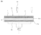
FIG. 10 is a schematic front sectional view of a sputtering apparatus used for forming a reinforcing annular insulating film pattern in the method of manufacturing a semiconductor device according to one embodiment of the present application. FIG. 11 is a schematic front sectional view of a plasma CVD apparatus used for forming an insulating film that is a base of a reinforcing annular insulating film pattern in the method for manufacturing a semiconductor device according to an embodiment of the present application.
図10のスパッタリング装置51は、直接、ウエハ1上に、補強用環状絶縁膜パターン15(図12参照)を形成できる点が特徴である。このスパッタリング成膜処理は、いわゆる反応性スパッタリング成膜である。図10に示すように、スパッタ成膜チャンバ52の内部下方には、回転軸59に保持された下部電極(ウエハ・ステージ)53があり、その上には、複数枚の被処理ウエハ1がその裏面1bを上にしてセットされている。この下部電極53は接地されている。スパッタ成膜チャンバ52の内部上方には、シリコン・ターゲット55をその下面に保持した上部電極(ターゲット・バッキング・プレート)54が設けられている。この上部電極54は直流電源67の負極に接続されており、直流電源67の正極は接地されている。上部電極54と下部電極53の間であって下部電極53に近接した位置には、固定シャッタ56が設けられており、その一部はシャドー・マスク57となっている。その周辺の円環状の開口58(数箇所は微細なリード状の支持部材で周辺部に保持されている)の存在により、その直下のウエハ1の裏面(第2の主面)1bの周辺部にのみ窒化シリコン膜がスパッタ成膜されるようになっている。他のウエハを処理するときは、目的のウエハがシャドー・マスク57の直下に来るように、回転軸59によってウエハ・ステージ53を回転させる。
The
窒化シリコン膜の反応性スパッタリング成膜処理を実施する際には、ガス導入口68より窒素ガスを供給しながら、排気口69より真空排気系によりスパッタ成膜チャンバ52内を所定の真空度になるように真空引きする。
When the reactive sputtering film forming process of the silicon nitride film is performed, the inside of the sputter
図11のプラズマCVD装置71は、補強用環状絶縁膜パターン15(図12参照)を全面一様膜形成と通常のリソグラフィの組み合わせにより、形成する場合に使用する窒化シリコン膜成膜用のプラズマCVD装置の一例である。図11に示すように、プラズマCVD成膜チャンバ76の内部下方には、下部電極(ウエハ・ステージ)72があり、その上には、被処理ウエハ1がその裏面1bを上にしてセットされている。この下部電極53は接地されている。プラズマCVD成膜チャンバ76の内部上方には、その下端にシャワー・ヘッド77を有する上部電極73が設けられている。この上部電極73は、たとえば高周波電源74(13.56MHz)および低周波電源75(250kHz)に接続されている(いずれか一方をオンすることも、両方オン又はオフすることも可能にされている)。これらの各電源の他端は接地されている。上部電極73にはガス導入口78が設けられており、成膜時には、ここから反応ガスが供給される。また、成膜時には、排気口79より真空排気系によりプラズマCVD成膜チャンバ76内を所定の真空度になるように真空引きする。
The
3.本願の一実施の形態の半導体装置の製造方法のプロセス・フロー等の説明(主に図3、図4から図9、および図12から図20)
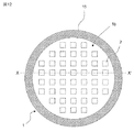
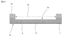
図3は、本願の一実施の形態の半導体装置の製造方法の主要プロセス・ブロック・フロー図である。図12は図3に対応するデバイス裏面図であり、図19は、図3に対応するデバイス表面(表側面)図(ダイシング工程)である。図4から図9、図13から図18、および図20は、図3に対応するデバイス断面プロセス・フロー図である。図12は、図3に対応するデバイス裏面図(補強用環状絶縁膜パターン形成完了時点)である。図19は、図3に対応するデバイス表面(表側面)図(ダイシング工程)である。これらのうち図13は図12のX−X’に対応するデバイス断面図であり、図20は図19のX−X’に対応するデバイス断面図である。以下では、ウエハの反りという観点から製造プロセスの要部等を説明する。ここでは、200φウエハを例にとり説明する。
3. Description of process flow of semiconductor device manufacturing method according to one embodiment of the present application (mainly FIG. 3, FIG. 4 to FIG. 9, and FIG. 12 to FIG. 20)
FIG. 3 is a main process block flow diagram of the semiconductor device manufacturing method according to the embodiment of the present application. FIG. 12 is a device rear view corresponding to FIG. 3, and FIG. 19 is a device surface (front side) view (dicing step) corresponding to FIG. 4-9, 13-18, and 20 are device cross-sectional process flow diagrams corresponding to FIG. FIG. 12 is a rear view of the device corresponding to FIG. 3 (when the reinforcing annular insulating film pattern is completely formed). FIG. 19 is a device surface (front side) view (dicing step) corresponding to FIG. 3. 13 is a device cross-sectional view corresponding to XX ′ in FIG. 12, and FIG. 20 is a device cross-sectional view corresponding to XX ′ in FIG. Below, the main part of a manufacturing process etc. are demonstrated from a viewpoint of the curvature of a wafer. Here, a 200φ wafer will be described as an example.
まず、図3に示すように、ウエハ表面処理工程群101(第1の主面処理工程群)は、種々の工程から構成されているが、ウエハのそりに主に寄与しているのは、ウエハ表面金属膜形成工程101a(第1の金属膜形成工程)であるので、図1の表面金属膜3(第1の金属膜)を形成する前の状態から説明する。図4に示すように、N型単結晶シリコン基板1の表側1a(第1の主面又はデバイス面)には半導体素子領域2(チップ領域)が形成されている。この段階では、図1の裏面金属膜4(第2の金属膜)、裏面側P+領域6p、埋め込みN+領域6n、表面金属膜3(第1の金属膜)等は、まだ形成されていない。ウエハ径は、150φ(直径約150ミリ・メートルのほぼ円板形状)の場合を例にとり具体的に説明するが、150φの外、100φ、200φ、300φ、450φ等が利用可能である。
First, as shown in FIG. 3, the wafer surface treatment process group 101 (first main surface treatment process group) is composed of various processes, and the main contribution to the wafer warpage is as follows. Since it is the wafer surface metal
次に、図5に示すように、ウエハ1の表面側1aのほぼ全面に、表面金属膜3(第1の金属膜)を、たとえば、スパッタ成膜等により形成する(図3の第1の金属膜形成工程101a)。表面金属膜3の構成としては、下層のバリア・メタル膜(たとえばTiW,Ti/TiN複合膜)、上層のアルミニウム系メタル膜(たとえば、シリコン添加アルミニウム、銅添加アルミニウムなど)等から構成されるものを例示することができる。厚さは、たとえば、下層のバリア・メタル膜が、たとえば200nm程度(好適な範囲としては100nmから300nm程度)であり、上層のアルミニウム系メタル膜が、たとえば1200nm程度(好適な範囲としては1000nmから3000nm程度)である。
Next, as shown in FIG. 5, a surface metal film 3 (first metal film) is formed on almost the
その後、表面金属膜3は通常のリソグラフィにより、パターニングされる。その後、必要に応じてファイナル・パッシベーション膜の形成および加工等を実施する。
Thereafter, the
次に、図3のバック・グラインディング工程群102に入る。図6に示すように、まず、基体31a、粘着層31b等からなるBG保護テープ31(ウエハ表面保護テープ)をウエハ1の表面側1aのほぼ全面に貼り付ける(図3のウエハ表面への研削保護テープ貼り付け工程102a)。この時点のウエハの厚さは、第1の厚さである。この時点では、ウエハの厚さが比較的厚いので、ウエハのそりが、搬送や具体的な処理に大きく影響することは比較的少ない。なお、ウエハの第1の厚さは、ここでは、たとえば、550マイクロ・メートル程度であり、通常、230マイクロ・メートル以上、1ミリ・メートル未満程度の範囲が好適である。
Next, the process enters the back grinding
この状態で、図7に示すように、バック・グラインディング工程102b(図3)を実行する。図7に示すように、回転するウエハ吸着回転テーブル62にウエハ1の表面側1aを吸着した状態で、ウエハ1の裏面1b(第2の主面)をBGホイール61により研削することで、ウエハの厚さを第1の厚さよりも薄い第2の厚さとする。ウエハの第2の厚さは、ここでは、たとえば、150マイクロ・メートル程度であり、通常、70マイクロ・メートル以上、230マイクロ・メートル未満程度の範囲(好ましくは100マイクロ・メートル以上、200マイクロ・メートル未満程度の範囲)が好適である。
In this state, as shown in FIG. 7, the
次に、図8に示すように、バック・グラインディング工程102b(図3)にできたダメージ層を除去するためのストレス・リリーフ工程102c(図3)を実施する。ストレス・リリーフには種々の方法があるが、たとえば、図7に示すように、エッチング回転ステージ63上にBG保護テープ31が付いた状態のウエハ1のデバイス面1aを吸着した状態で、エッチング薬液ノズル64により、ウエハ1の裏面1bにシリコン・エッチング液を供給する方法によって、表面の薄いダメージ層を除去する。
Next, as shown in FIG. 8, a
次に、図3のBGテープ剥離工程102dを実行する。図9に示すように、たとえば、加熱されたウエハ吸着ステージ65上に、ウエハ1の裏面1bを吸着した状態で、ウエハ表面保護テープ31を全面剥離する。この時点で、ウエハ1は、表面側1aのみに厚いメタル膜が形成された状態であり、ウエハが薄くなっているので、そりの影響が出てくることが予想される。
Next, the BG
そこで、図3のウエハ補強膜成膜工程103(ウエハ補強膜パターン形成工程)を、たとえばセクション2で説明したいずれかの装置を使用して実行する。図12および図13に示すように、ウエハ1の裏面1b(第2の主面)に、裏面1bの周辺に沿って円環状の無機系絶縁膜パターン15(たとえば、窒化シリコン膜等の窒化シリコン系絶縁膜)を形成する。従って、円環状の絶縁膜パターン15の内部には円形開口16が存在する。有機系絶縁膜と異なり、無機系絶縁膜、特に窒化シリコン系絶縁膜は、応力が比較的強く、比較的薄い膜でも強い応力を付与することができる。また、窒化シリコン系絶縁膜は、スパッタ成膜時の圧力やガス流量等を制御することにより、比較的簡単に応力値を変化させることができるというメリットがある。
Therefore, the wafer reinforcing film forming step 103 (wafer reinforcing film pattern forming step) in FIG. 3 is executed using, for example, any of the apparatuses described in
なお、反り緩和用の絶縁膜パターン15は、図10に示したようなシャドー・マスクを用いたスパッタ成膜(選択的膜形成)によって、比較的単純なプロセスで形成することができる。このときの成膜の諸条件としては、たとえば膜厚500nm程度(円環状の絶縁膜パターン15の幅は、たとえば4ミリ・メートル程度)、引張膜応力200Mパスカル程度、真空度0.2パスカル程度、ウエハ・ステージ温度摂氏150度程度、印加電力300ワット程度、窒素ガス流量35sccm程度、アルゴン・ガス流量15sccm程度、成膜時間170分程度を例示することができる。
The warp mitigating insulating
また、反り緩和用の絶縁膜パターン15は、図11に例示するようなCVD装置を使用したCVD(プラズマCVD)とリソグラフィの組み合わせによる2段階のプロセスによって、特別な装置を使用しないで形成することもできる。成膜時間もCVDの方がはるかに早い。また、選択的でないスパッタ成膜とリソグラフィの組み合わせによる2段階のプロセスによって、特別な装置を使用しないで形成することもできる。このときの成膜の諸条件(図11の装置によるもの)としては、たとえば膜厚1200nm程度(円環状の絶縁膜パターン15の幅は、たとえば4ミリ・メートル程度)、引張膜応力200Mパスカル程度、真空度350パスカル程度、ウエハ・ステージ温度摂氏400度程度、高周波印加電力(13.56MHz)300ワット程度、低周波印加電力(250kHz)300ワット程度、窒素ガス流量1600sccm程度、モノシラン・ガス流量500sccm程度、アンモニア・ガス流量4500sccm程度、成膜時間11分程度を例示することができる。
Further, the insulating
この反り緩和用の絶縁膜パターン15によって、ウエハ1に表面金属膜3と逆の反りが付与されるので、反り相殺の結果、特別なサポート板等がない状態でもハンドリングや処理のための保持が容易となる。
The warp mitigating insulating
反り緩和用の絶縁膜パターン15は、円環状を例示したが、幾何学的な円環のみを指すものではなく、たとえば、ウエハ周辺の製品チップ不在領域(チップ不在領域および非製品チップ領域)に対応する略円環様の図形でもよい。
The insulating
次に、このように比較的そりのない状態(この時点のウエハの厚さは第2の厚さと実質的に同じ)にした後に、図14に示すように、最終的なデバイス厚さに相当する第3の厚さ(第2の厚さよりも薄い)まで多数の半導体素子領域2が存在するウエハ1の裏面1b(第2の主面)、すなわち、円形開口16の部分を研削(たとえば、ホイールによるバック・グラインディング)やエッチング(たとえばウエット・エッチング)により減厚処理する(図3のウエハ裏面エッチング工程104)。ウエハの第3の厚さは、ここでは、たとえば、85マイクロ・メートル程度であり、通常、200マイクロ・メートル未満、30マイクロ・メートル以上程度の範囲が好適である。このように、ウエハを薄くするのは、デバイスのオン抵抗を下げる等のためである。
Next, after making such a relatively warp-free state (the thickness of the wafer at this point is substantially the same as the second thickness), as shown in FIG. 14, it corresponds to the final device thickness. The
次に、図3のウエハ裏面イオン注入工程群105の処理に移る。まず、裏面側P+領域6pの形成のためのウエハ裏面イオン注入工程105aを実行する。図15に示すように、ウエハ吸着ステージ81にウエハ1のデバイス面1aを吸着した状態で、ウエハ1の裏面1bに、たとえば所定のP型不純物等をイオン注入する。この際、ウエハ1の裏面1bに、反り緩和用の絶縁膜パターン15があるので、イオン注入装置等へのウエハの搬入、内部での保持(静電吸着)、搬出等において支障をきたすことがない。続いて、図3のウエハ裏面活性化アニール工程105bを実行する。
Next, the process proceeds to the wafer back surface ion
なお、図1の裏面側N+領域6nを形成する必要があるときは、先のウエハ裏面イオン注入工程群105と同様に、所定のN型不純物等をイオン注入およびアニールを繰り返せばよい。
When it is necessary to form the back surface side N +
次に、裏面金属膜形成の前処理として、図3のウエハ裏面酸化膜除去処理106を実行する。続いて、図16に示すように、ウエハ1の裏面1b(円形開口16)に、裏面金属膜(第2の金属膜)4をたとえばスパッタリング成膜により形成する(図3のウエハ裏面メタル膜成膜工程(第2の金属膜形成工程)107)。この裏面金属膜4の形成により、ウエハ1は、若干反るが、ウエハ1の裏面1bに、反り緩和用の絶縁膜パターン15があるので、基礎となるそり状態が比較的小さく、ハンドリングが困難になるほど大きなそりになることは比較的少ない。
Next, a wafer back surface oxide
次に、図3のウエハ・テスト工程108を実行する。図17に示すように、ウエハ・プローバ85のウエハ吸着ステージ88にウエハ1の裏面1bを吸着した状態で、表面プローブ針86および裏面プローブ針87をそれぞれウエハ1の表面1aおよび裏面1bの被テスト半導体素子領域2(チップ領域)にコンタクトして、電気的試験を実行する。この工程におけるウエハの反りの問題は、先の工程であるウエハ裏面酸化膜除去処理106とほぼ同じである。
Next, the
次に、図3のダイシング工程109(ペレタイズ工程)を実行する。図18に示すように、先ず、基材部92aと粘着剤層92bからなるダイシング・テープを貼り付けたダイシング・ウエハ保持フレーム91の粘着剤層92bにウエハ1の裏面1bを貼り付ける。この際、ウエハ1の裏面1bに、反り緩和用の絶縁膜パターン15があるので、基礎となるそり状態が比較的小さく、ハンドリングが困難になるほど大きなそりになることは比較的少なく、貼り付け作業は比較的容易に自動実行できる。この状態で、図19に示すように、たとえば、ウエハ1を縦・横のダイシング・ライン(スクライブ・ライン)に沿って、切断することによって、個々の半導体素子領域2(チップ領域)に分離する。すなわち、図20に示すように、ダイシング装置90の真空吸着ウエハ・ステージ95にウエハ1を固定したダイシング・ウエハ保持フレーム91を真空吸着した状態で、ダイシング・ブレード94でウエハ1を縦・横のダイシング・ライン(スクライブ・ライン)に沿って、切断する。なお、切断後は、チップ2のサイズは、比較的小さいので、反りが搬送やハンドリング上の大きな問題となることはない。なお、チップへの分離は、レーザ等を単独で、または、ブレード・ダイシングと組み合わせて行うものでもよい。
Next, the dicing process 109 (pelletizing process) of FIG. 3 is performed. As shown in FIG. 18, first, the
4.サマリ
以上本発明者によってなされた発明を実施形態に基づいて具体的に説明したが、本発明はそれに限定されるものではなく、その要旨を逸脱しない範囲において種々変更可能であることは言うまでもない。
4). Summary The invention made by the present inventor has been specifically described based on the embodiments. However, the present invention is not limited thereto, and it goes without saying that various changes can be made without departing from the scope of the invention.
例えば、前記実施の形態においては、プレーナ型のIGBTデバイスに例をとり具体的に説明したが、本発明はそれに限定されるものではなく、トレンチ・ゲート型のIGBTデバイス等にも同様に適用できることは言うまでもない。また、前記実施の形態においては、パワー・トランジスタ・デバイスの一例としてIGBTデバイスに例をとり具体的に説明したが、本発明はそれに限定されるものではなく、プレーナ型やトレンチ・ゲート型のパワーMOSFET(パワーMISFET)等にも同様に適用できることは言うまでもない。なお、前記実施の形態においては、シリコン系ウエハ等の単結晶基板(具体的にはN型単結晶シリコン・ウエハ)を用いた例を説明したが、本発明はそれに限定されるものではなく、シリコン系のエピタキシャル基板やGaAs系の化合物半導体基板を用いたものにも同様に適用できることは言うまでもない。また、前記実施の形態においては、ワイヤ・ボンディングにより外部と接続されることを予定したワイヤ接続型のデバイスを例にとり具体的に説明したが、チップ上面のメタル電極上に更にニッケル等のUBM(Under Bump Metal)膜を設け、その上にバンプ電極等を形成したバンプ品にも適用できることは言うまでもない。更に、前記実施の形態においては、上面の主要な金属膜として、アルミニウム系の金属膜を比較的厚く、かつ、広い面積に形成する一例を示したが、本発明はそれに限定されるものではなく、たとえば、銅系、またはTiW(たとえばチタン10%、タングステン90%)等のチタン系またはタングステン系などのリフラクトリ・メタルを用いたものにも適用できることは言うまでもない。
For example, in the above-described embodiments, the planar type IGBT device has been specifically described as an example. However, the present invention is not limited thereto, and can be similarly applied to a trench gate type IGBT device or the like. Needless to say. In the above-described embodiment, an IGBT device has been specifically described as an example of a power transistor device. However, the present invention is not limited to this, and a planar type or trench gate type power is described. Needless to say, the present invention can be similarly applied to a MOSFET (power MISFET) or the like. In the above embodiment, an example using a single crystal substrate such as a silicon-based wafer (specifically, an N-type single crystal silicon wafer) has been described. However, the present invention is not limited thereto, Needless to say, the present invention can be similarly applied to a silicon-based epitaxial substrate or a GaAs-based compound semiconductor substrate. In the above-described embodiment, the wire connection type device that is expected to be connected to the outside by wire bonding has been specifically described as an example. Needless to say, the present invention can also be applied to a bump product in which a bumper metal (Under Bump Metal) film is provided and a bump electrode or the like is formed thereon. Furthermore, in the above-described embodiment, an example in which an aluminum-based metal film is formed to be relatively thick and has a large area as the main metal film on the upper surface has been described, but the present invention is not limited thereto. For example, it is needless to say that the present invention can also be applied to a material using a refractory metal such as copper or TiW (eg,
1 半導体ウエハまたはチップ(半導体基板)
1a ウエハ(またはチップ)の表面又は表側(第1の主面又はデバイス面)
1b ウエハ(またはチップ)の裏面(第2の主面)
1s N型単結晶シリコン基板部
2 半導体素子領域(チップ領域)
3 表面金属膜(第1の金属膜)
4 裏面金属膜(第2の金属膜)
5 ゲート・ポリシリコン膜
6p 裏面側P+領域
6n 裏面側N+領域(埋め込みN+領域)
7 N型ドリフト領域
8 チャネル領域
9 P型ベース領域
10 IGBT素子
10b IGBT素子のバイポーラ・トランジスタ部分
10m IGBT素子のMOSFET部分
11 N+エミッタ領域
12 ディープP+領域
14 ゲート周辺絶縁膜(ゲート絶縁膜および層間絶縁膜)
15 第1の絶縁膜(絶縁膜パターン)
16 円環状絶縁膜パターンの中央部の円形開口(またはその部分に対応するウエハ)
31 BG保護テープ(ウエハ表面保護テープ)
31a BG保護テープの基体
31b BG保護テープの粘着層
51 スパッタ成膜装置
52 スパッタ成膜チャンバ
53 スパッタ成膜装置の下部電極(ウエハ・ステージ)
54 スパッタ成膜装置の上部電極(ターゲット・バッキング・プレート)
55 ターゲット
56 シャッタ
57 シャドー・マスク
58 円環状開口
59 回転軸
61 BGホイール
62 BGウエハ吸着回転テーブル
63 ストレス・リリーフ用エッチング回転ステージ
64 ストレス・リリーフ用エッチング薬液ノズル
65 剥離装置のウエハ吸着ステージ
67 直流電源
68 ガス導入口
69 排気口
71 プラズマCVD装置
72 プラズマCVD装置の下部電極(ウエハ・ステージ)
73 プラズマCVD装置の上部電極
74 高周波電源(13.56MHz)
75 低周波電源(250kHz)
76 プラズマCVD装置の処理チャンバ
77 シャワー・ヘッド
78 ガス導入口
79 排気口
81 イオン注入装置のウエハ吸着ステージ
85 ウエハ・プローバ
86 表面プローブ針
87 裏面プローブ針
88 ウエハ・プローバのウエハ吸着ステージ
90 ダイシング装置
91 ダイシング・ウエハ保持フレーム
92 ダイシング・テープ
92a ダイシング・テープの基材部
92b ダイシング・テープの粘着剤層
94 ダイシング・ブレード
95 真空吸着ウエハ・ステージ
101 ウエハ表面処理工程群(第1の主面処理工程群)
101a ウエハ表面金属膜形成工程(第1の金属膜形成工程)
102 バック・グラインディング工程群
102a ウエハ表面への研削保護テープ貼り付け工程
102b バック・グラインディング工程
102c ストレス・リリーフ工程
102d BGテープ剥離工程
103 ウエハ補強膜成膜工程(ウエハ補強膜パターン形成工程)
104 ウエハ裏面エッチング工程
105 ウエハ裏面イオン注入工程群
105a ウエハ裏面イオン注入工程
105b ウエハ裏面活性化アニール工程
106 ウエハ裏面酸化膜除去
107 ウエハ裏面メタル膜成膜工程(第2の金属膜形成工程)
108 ウエハ・テスト工程
109 ダイシング工程(ペレタイズ工程)
C コレクタ端子(コレクタ電極)
E エミッタ端子(エミッタ電極)
G ゲート端子(ゲート電極)
1 Semiconductor wafer or chip (semiconductor substrate)
1a Wafer (or chip) surface or front side (first main surface or device surface)
1b Back surface (second main surface) of wafer (or chip)
1s N-type single crystal
3 Surface metal film (first metal film)
4 Back metal film (second metal film)
5 Gate /
7 N-
15 First insulating film (insulating film pattern)
16 A circular opening in the center of the annular insulating film pattern (or a wafer corresponding to that portion)
31 BG protective tape (wafer surface protective tape)
31a Base of BG
54 Upper electrode of sputtering sputter deposition system (target backing plate)
55
73 Upper electrode of
75 Low frequency power supply (250 kHz)
76 Processing chamber of
101a Wafer surface metal film forming step (first metal film forming step)
102 Back Grinding
104 Wafer Back
108
C Collector terminal (collector electrode)
E Emitter terminal (emitter electrode)
G Gate terminal (gate electrode)
Claims (1)
(a)第1の厚さを有する半導体ウエハの第1の主面上に、第1の金属膜を形成する工程;
(b)前記工程(a)の後、前記半導体ウエハの第2の主面側に対して、バック・グラインディング処理を実行することにより、前記第1の厚さよりも薄い第2の厚さとする工程;
(c)前記工程(b)の後、前記半導体ウエハの前記第2の主面上に、その周辺に沿って、第1の絶縁膜からなり、前記第2の主面の周辺に沿う円環状絶縁膜パターンを含む絶縁膜パターンを形成する工程;
(d)前記絶縁膜パターンがある状態で、前記円環状絶縁膜パターンの開口部の厚さを前記第2の厚さよりも薄い第3の厚さとする工程;
(e)前記工程(d)の後、前記絶縁膜パターンがある状態で、前記半導体ウエハに対して、電気的テストを実行する工程;
(f)前記工程(e)の後、前記絶縁膜パターンがある状態で、前記半導体ウエハの前記第2の主面を粘着シートに貼り付けることにより、前記粘着シートを介してダイシング・フレームに保持させる工程;
(g)前記工程(f)の後、ダイシング・フレームに保持された状態で、前記半導体ウエハを個々のチップに分割する工程。 A semiconductor device manufacturing method including the following steps:
(A) forming a first metal film on a first main surface of a semiconductor wafer having a first thickness;
(B) After the step (a), by performing a back-grinding process on the second main surface side of the semiconductor wafer, a second thickness smaller than the first thickness is obtained. Process;
(C) After the step (b), an annular shape is formed on the second main surface of the semiconductor wafer along the periphery along the periphery of the semiconductor wafer and along the periphery of the second main surface. Forming an insulating film pattern including an insulating film pattern;
(D) a step of setting the thickness of the opening of the annular insulating film pattern to a third thickness smaller than the second thickness in a state where the insulating film pattern is present;
(E) after the step (d), performing an electrical test on the semiconductor wafer in a state where the insulating film pattern is present;
(F) After the step (e), the second main surface of the semiconductor wafer is attached to the adhesive sheet in a state where the insulating film pattern exists, and is held on the dicing frame via the adhesive sheet. The step of causing;
(G) After the step (f), the step of dividing the semiconductor wafer into individual chips while being held by a dicing frame.
Priority Applications (3)
| Application Number | Priority Date | Filing Date | Title |
|---|---|---|---|
| JP2009101679A JP5431777B2 (en) | 2009-04-20 | 2009-04-20 | Manufacturing method of semiconductor device |
| US12/719,067 US8039276B2 (en) | 2009-04-20 | 2010-03-08 | Manufacturing method of semiconductor device |
| US13/237,235 US8153452B2 (en) | 2009-04-20 | 2011-09-20 | Manufacturing method of semiconductor device |
Applications Claiming Priority (1)
| Application Number | Priority Date | Filing Date | Title |
|---|---|---|---|
| JP2009101679A JP5431777B2 (en) | 2009-04-20 | 2009-04-20 | Manufacturing method of semiconductor device |
Publications (3)
| Publication Number | Publication Date |
|---|---|
| JP2010251632A JP2010251632A (en) | 2010-11-04 |
| JP2010251632A5 JP2010251632A5 (en) | 2012-04-12 |
| JP5431777B2 true JP5431777B2 (en) | 2014-03-05 |
Family
ID=42981301
Family Applications (1)
| Application Number | Title | Priority Date | Filing Date |
|---|---|---|---|
| JP2009101679A Active JP5431777B2 (en) | 2009-04-20 | 2009-04-20 | Manufacturing method of semiconductor device |
Country Status (2)
| Country | Link |
|---|---|
| US (2) | US8039276B2 (en) |
| JP (1) | JP5431777B2 (en) |
Cited By (1)
| Publication number | Priority date | Publication date | Assignee | Title |
|---|---|---|---|---|
| US11081344B2 (en) | 2018-01-25 | 2021-08-03 | Fujifilm Business Innovation Corp. | Method for manufacturing semiconductor substrate |
Families Citing this family (17)
| Publication number | Priority date | Publication date | Assignee | Title |
|---|---|---|---|---|
| FR2953064B1 (en) * | 2009-11-20 | 2011-12-16 | St Microelectronics Tours Sas | METHOD FOR ENCAPSULATING ELECTRONIC COMPONENTS ON WAFER |
| JP5898679B2 (en) * | 2011-06-02 | 2016-04-06 | デンカ株式会社 | Adhesive tape and semiconductor wafer processing method |
| JP5755043B2 (en) * | 2011-06-20 | 2015-07-29 | 株式会社ディスコ | Processing method of semiconductor wafer |
| JP5846060B2 (en) | 2011-07-27 | 2016-01-20 | 信越化学工業株式会社 | Wafer processing body, wafer processing member, wafer processing temporary adhesive, and thin wafer manufacturing method |
| JP5464192B2 (en) * | 2011-09-29 | 2014-04-09 | 株式会社デンソー | Manufacturing method of semiconductor device |
| JP5893887B2 (en) * | 2011-10-11 | 2016-03-23 | ルネサスエレクトロニクス株式会社 | Manufacturing method of semiconductor device |
| JP5687647B2 (en) * | 2012-03-14 | 2015-03-18 | 株式会社東芝 | Semiconductor device manufacturing method and semiconductor manufacturing apparatus |
| JP5591852B2 (en) * | 2012-03-19 | 2014-09-17 | 株式会社東芝 | Semiconductor device inspection method, semiconductor device manufacturing method, inspection jig |
| US9318446B2 (en) | 2013-03-15 | 2016-04-19 | Infineon Technologies Austria Ag | Metal deposition on substrates |
| JP6304445B2 (en) * | 2015-03-16 | 2018-04-04 | 富士電機株式会社 | Manufacturing method of semiconductor device |
| WO2016169818A1 (en) * | 2015-04-24 | 2016-10-27 | Abb Technology Ag | Power semiconductor device with thick top-metal-design and method for manufacturing such power semiconductor device |
| DE102015112649B4 (en) * | 2015-07-31 | 2021-02-04 | Infineon Technologies Ag | METHOD OF FORMING A SEMICONDUCTOR COMPONENT AND A SEMICONDUCTOR COMPONENT |
| JP6658171B2 (en) | 2016-03-22 | 2020-03-04 | 富士電機株式会社 | Method for manufacturing semiconductor device |
| WO2019142556A1 (en) * | 2018-01-17 | 2019-07-25 | Sppテクノロジーズ株式会社 | Wide-gap semiconductor substrate, apparatus for manufacturing wide-gap semiconductor substrate, and method for manufacturing wide-gap semiconductor substrate |
| JP7200537B2 (en) * | 2018-08-21 | 2023-01-10 | 富士フイルムビジネスイノベーション株式会社 | Semiconductor substrate manufacturing method |
| US20200321236A1 (en) * | 2019-04-02 | 2020-10-08 | Semiconductor Components Industries, Llc | Edge ring removal methods |
| CN110676207B (en) * | 2019-09-27 | 2021-11-16 | 云谷(固安)科技有限公司 | Separation device and separation method |
Family Cites Families (15)
| Publication number | Priority date | Publication date | Assignee | Title |
|---|---|---|---|---|
| JP3184493B2 (en) * | 1997-10-01 | 2001-07-09 | 松下電子工業株式会社 | Electronic device manufacturing method |
| US6162702A (en) * | 1999-06-17 | 2000-12-19 | Intersil Corporation | Self-supported ultra thin silicon wafer process |
| JP3834589B2 (en) * | 2001-06-27 | 2006-10-18 | 株式会社ルネサステクノロジ | Manufacturing method of semiconductor device |
| DE10256985B4 (en) * | 2001-12-12 | 2013-01-10 | Denso Corporation | Method for producing a power semiconductor component |
| JP3620528B2 (en) | 2001-12-12 | 2005-02-16 | 株式会社デンソー | Manufacturing method of semiconductor device |
| US6884717B1 (en) * | 2002-01-03 | 2005-04-26 | The United States Of America As Represented By The Secretary Of The Air Force | Stiffened backside fabrication for microwave radio frequency wafers |
| JP2004186522A (en) * | 2002-12-05 | 2004-07-02 | Renesas Technology Corp | Manufacture method of semiconductor device |
| JP4570896B2 (en) * | 2004-04-06 | 2010-10-27 | ルネサスエレクトロニクス株式会社 | Manufacturing method of semiconductor device |
| JP2005303218A (en) * | 2004-04-16 | 2005-10-27 | Renesas Technology Corp | Semiconductor device and its manufacturing method |
| JP4020097B2 (en) | 2004-05-11 | 2007-12-12 | セイコーエプソン株式会社 | Semiconductor chip, semiconductor device, manufacturing method thereof, and electronic device |
| JPWO2006008824A1 (en) * | 2004-07-16 | 2008-05-01 | 株式会社ルネサステクノロジ | Manufacturing method of semiconductor integrated circuit device |
| JP4904922B2 (en) | 2006-05-26 | 2012-03-28 | トヨタ自動車株式会社 | Semiconductor substrate manufacturing method and semiconductor substrate |
| JP4816278B2 (en) * | 2006-06-15 | 2011-11-16 | 富士電機株式会社 | Manufacturing method of semiconductor device |
| JP2008053595A (en) | 2006-08-28 | 2008-03-06 | Toyota Motor Corp | Semiconductor wafer, and its manufacturing method |
| JP5007179B2 (en) * | 2007-08-29 | 2012-08-22 | ルネサスエレクトロニクス株式会社 | Manufacturing method of semiconductor device |
-
2009
- 2009-04-20 JP JP2009101679A patent/JP5431777B2/en active Active
-
2010
- 2010-03-08 US US12/719,067 patent/US8039276B2/en active Active
-
2011
- 2011-09-20 US US13/237,235 patent/US8153452B2/en active Active
Cited By (1)
| Publication number | Priority date | Publication date | Assignee | Title |
|---|---|---|---|---|
| US11081344B2 (en) | 2018-01-25 | 2021-08-03 | Fujifilm Business Innovation Corp. | Method for manufacturing semiconductor substrate |
Also Published As
| Publication number | Publication date |
|---|---|
| US20120009695A1 (en) | 2012-01-12 |
| US8039276B2 (en) | 2011-10-18 |
| US8153452B2 (en) | 2012-04-10 |
| JP2010251632A (en) | 2010-11-04 |
| US20100267175A1 (en) | 2010-10-21 |
Similar Documents
| Publication | Publication Date | Title |
|---|---|---|
| JP5431777B2 (en) | Manufacturing method of semiconductor device | |
| JP4185704B2 (en) | Manufacturing method of semiconductor device | |
| US8507362B2 (en) | Process of forming ultra thin wafers having an edge support ring | |
| JP5712058B2 (en) | Manufacturing method of semiconductor device | |
| PH12013000169A1 (en) | Semiconductor die singulation method | |
| US7737531B2 (en) | Wafer including a reinforcing flange formed upright at a periphery and method for manufacturing the same | |
| US20140134828A1 (en) | Semiconductor die singulation method | |
| JP2010267899A (en) | Method of manufacturing semiconductor device | |
| US10032670B2 (en) | Plasma dicing of silicon carbide | |
| JP2014007351A (en) | Semiconductor device manufacturing method | |
| JP3620528B2 (en) | Manufacturing method of semiconductor device | |
| CN107968048A (en) | A kind of method for reducing semiconductor devices back metal contacts resistance | |
| US20200321236A1 (en) | Edge ring removal methods | |
| JP6028325B2 (en) | Manufacturing method of semiconductor device | |
| JP4724729B2 (en) | Manufacturing method of semiconductor device | |
| US11710656B2 (en) | Method of forming semiconductor-on-insulator (SOI) substrate | |
| US20220336265A1 (en) | Method of forming semiconductor-on-insulator (soi) substrate | |
| JP2002100773A (en) | Semiconductor device and its manufacturing method | |
| JP2013093442A (en) | Semiconductor device manufacturing method | |
| JP2013041919A (en) | Semiconductor device manufacturing method | |
| JP2007266347A (en) | Method of manufacturing semiconductor device | |
| JP2010272676A (en) | Method of manufacturing semiconductor device | |
| JP2011138976A (en) | Method of manufacturing semiconductor device | |
| JP2009260041A (en) | Method of manufacturing semiconductor device, and film formation device | |
| WO2014012425A1 (en) | Method for manufacturing field stop igbt |
Legal Events
| Date | Code | Title | Description |
|---|---|---|---|
| A521 | Written amendment |
Free format text: JAPANESE INTERMEDIATE CODE: A523 Effective date: 20120229 |
|
| A621 | Written request for application examination |
Free format text: JAPANESE INTERMEDIATE CODE: A621 Effective date: 20120229 |
|
| A977 | Report on retrieval |
Free format text: JAPANESE INTERMEDIATE CODE: A971007 Effective date: 20131007 |
|
| TRDD | Decision of grant or rejection written | ||
| A01 | Written decision to grant a patent or to grant a registration (utility model) |
Free format text: JAPANESE INTERMEDIATE CODE: A01 Effective date: 20131114 |
|
| A977 | Report on retrieval |
Free format text: JAPANESE INTERMEDIATE CODE: A971007 Effective date: 20131125 |
|
| A61 | First payment of annual fees (during grant procedure) |
Free format text: JAPANESE INTERMEDIATE CODE: A61 Effective date: 20131205 |
|
| R150 | Certificate of patent or registration of utility model |
Free format text: JAPANESE INTERMEDIATE CODE: R150 Ref document number: 5431777 Country of ref document: JP Free format text: JAPANESE INTERMEDIATE CODE: R150 |
|
| S531 | Written request for registration of change of domicile |
Free format text: JAPANESE INTERMEDIATE CODE: R313531 |
|
| R350 | Written notification of registration of transfer |
Free format text: JAPANESE INTERMEDIATE CODE: R350 |